
Submitted:
24 March 2025
Posted:
26 March 2025
You are already at the latest version
Abstract
The quantum efficiency (QE) or gain (G) of a photoconductive device is most commonly
given in literature as a ratio of carrier lifetime to transit time, allowing for a value much greater than unity. In this work, by assuming primary photoconductivity, we reexamine the photoconductive theory for the device with an intrinsic (undoped) semiconductor, with nearly zero equilibrium carrier densities. Analytic gain formula is obtained for arbitrary drift and diffusion parameters under a bias voltage and by neglecting the polarization effect due to the relative displacement in the electron and hole distributions. We find that the lifetime/transit-time ratio formula is only valid in the limit of weak field and no diffusion. Numerical simulations are performed to examine the polarization effect, confirming that it does not change the qualitative conclusions. We discuss the distinction between two QE definitions used in the literature: accumulative QE (〖QE〗_acc ), considering the contributions of the flow of all photocarriers, regardless of whether they reach the electrode; and apparent QE (〖QE〗_app), measuring the photocurrent at the electrode. In general, 〖QE〗_acc>〖QE〗_app, due to an inhomogeneous photocurrent in the channel; however, both approach the same unity limit for strong drift. We find that 〖QE〗_acc 〖 QE〗_app is a deficiency of the commonly adopted constant-carrier-lifetime approximation in the recombination terms.
Keywords:
Photoconductive gain
; intrinsic semiconductor
; drift‐diffusion equations
1. Introduction
A photoconductive device is a special type of photodetector that consists of a metal-semiconductor-metal (M-S-M) structure [1,2,3,4,5]. The quantum efficiency or gain of a photoconductive device has been observed for over 150 years in a wide variety of materials [6]; however, the photoconductive gain theory still exhibits considerable controversy and ambiguity in literature. The quantum efficiency is defined as , where and are numbers of photogenerated carriers and absorbed photons per unit time, respectively. The gain is also commonly expressed as the ratio of the carrier recombination lifetime to the carrier transit time over the conductive channel [2,7,8,9,10,11,12,13,14]
If both electrons and holes are considered, is then given as [2,8,12,13]
where and are the electron and hole lifetimes, respectively, whilst and are their respective transit times from one electrode to another. This simplistic equation implies that can be increased by increasing and/or by decreasing . Since its initial appearance [11], Eq. (1) has been widely used to explain the experimentally observed photoconductive gains for various devices: due to a long recombination lifetime [8,12,13], a short transit time by having a high carrier mobility [8,12], by increasing applied voltage [15], or by shortening channel length of the device [7,12,15]. Additionally, carrier trapping within the photoconductive channel (e.g., on the surface), thought to increase , is often used as the mechanism for the observed high gain [8].
However, Eq. (1) cannot be derived rigorously from the drift-diffusion equations with photoexcitation that govern the carrier motions. By adopting an ambipolar-transport approximation, approximate analytic solutions of the drift-diffusion equations can be obtained for cases with high background carriers from either doping or thermal excitation [3,16]. Furthermore, Eq. (1) is obtained under two questionable assumptions: (1) when the detector is uniformly illuminated, the carrier distribution under an applied voltage remains uniform as in the zero-bias; (2) all carriers, no matter where they are generated (i.e., at any location relative to the electrodes), contribute equally to the photocurrent. The first assumption is invalid when realistic boundary conditions (BCs), such as vanishing BCs, are applied to the M-S contacts in solving the drift-diffusion equations [3,5,16,17]. More discussion on the BCs is given in the next section. The second assumption would be valid if the current of one carrier type alone could close the circuit without loss (e.g., all electrons exiting the anode return to the conduction band through the cathode). However, this assumption is inconsistent with the definition of primary photoconductivity [1,2,18,19], where one incident photon can create at most one electron-hole pair. In a steady state an electron and a hole are needed together to close the circuit. This implicitly assumes that a conduction band electron exiting from the anode can only return to the photoconductor through the cathode to the valence band, i.e., there is no carrier recycling within the same band. In this case, since electrons generated at a distance away from the collection electrode (i.e., anode) will decay in number while drifting toward the electrode, those generated at different distances from the electrode will contribute differently to the photocurrent. Specifically, for the carriers that either can or cannot reach the electrode, their contributions to the photocurrent are given by the ratio of their travel lengths toward collecting electrode to the channel length of the device [1,19,20,21].
To further understand the mechanism(s) of the photoconductive gain, we (re)examine a less well studied case of the photoconductive gain theory of a M-S-M device, with an intrinsic or undoped semiconductor that has negligible equilibrium carrier densities, allowing for arbitrary drift and diffusion conditions [1,16,17,19]. On the one hand, this is the case closest to primary photoconductivity, but, perhaps surprisingly, has not been studied in a comprehensive manner. For instance, previous studies often neglected the effect of diffusion [1,17,19,21]. On the other hand, when diffusion was included, high equilibrium carrier densities were assumed, to adopt an ambipolar approximation [16]. However, the minimal equilibrium carrier densities have some unique advantages for certain applications. High equilibrium carrier densities lead to a high dark current. Besides the well-known drawbacks such as reduced signal-to-noise ratio, increased power consumption, dynamic range limitation, and cooling requirements, the high dark current also prevents utilizing some unique effects of a photodetector with an exceptionally low dark current, as for instance, a recently reported optical logic and amplification functions under two or more light beam illumination [22,23]. For a photoconductive device with minimal equilibrium carrier densities, the key assumption, , of the ambipolar transport approximation [24] is invalid, because the distributions of the excess electrons and holes can exhibit significant relative displacement, a polarization effect, under an external field. Thus, the treatment required for the device of interest to this work is distinctly different from the devices with high background carrier densities, because the ambipolar-transport approximation is not applicable for the former case. In fact, the theory for the intrinsic semiconductor has a few tricky aspects that have not been properly discussed.
Furthermore, we note that in the literature, two subtly different definitions have been used, but without being explicitly distinguished. One definition, which we refer to as apparent quantum efficiency (), evaluates the photocurrent collected at the anode or cathode that should correspond to what is actually measured experimentally [19]. The other definition, which we refer to as accumulative quantum efficiency (), considers all photocurrents that ever flow in the device, regardless of whether they reach the electrodes [1,3,16,17,19,21].
Assuming uniform illumination, uniform electric field, constant carrier lifetime, negligible carrier diffusion and a BC of , the solution of the drift-only continuity equation for the excess distribution of holes (neglecting the label “p” in the subscripts of the parameters) is given below [17]
where is the photogeneration rate of electron-hole pairs, the drift length or carrier mean free path, the carrier mobility and the applied electric field. By evaluating the drift current at , where is the channel length of device, Eq. (2) would lead to , equivalent to , given below
In the limit of , one finds ; however, when , . Thus, if only the primary conductivity is considered, Eq. (1a) appears to be an inappropriately generalized low-drift limit result of Eq. (3).
On the other hand, the carrier distribution given by Eq. (2) can be used to calculate the photocurrent by averaging the carrier density over the channel length [17,21]. Based on this consideration, for one type of carrier (e.g., holes), without considering carrier diffusion, is given below as [17]
In fact, it can be shown that this spatial averaging scheme is equivalent to evaluate [1,19] (see Appendix), which yields the given by Eq. (4). Only in the limiting case of , one finds . On the other hand, when , one has . Therefore, if only the primary conductivity is considered, Eq. (1a) appears to be an inappropriately generalized low-drift limit result of Eq. (4). If both types of carriers have the same mobility and lifetime, or a mobility-lifetime product, they will contribute equally to the total , given as , which is limited to unity when . Consequently, Eq. (1b) appears to be an inappropriately generalized low conductivity limit result of Eq. (4) when both types of carriers are considered.
In this work, we adopt a few common approximations, such as uniform generation of electron-hole pairs, constant electric field, as well as constant carrier mobilities and lifetimes, independent of the electric field, carrier density, and position, as commonly adopted [1,16,17,19,21]. By solving the drift-diffusion equations of electrons and holes, under arbitrary conditions of drift and diffusion, we find analytic distributions of excess electrons and holes, as well as photocurrent of an intrinsic photoconductive device with negligible equilibrium carrier densities. We further show that the gain formula given by Eq. (1) is the low-drift limit result of the general expression, when the effect of diffusion is neglected. Additionally, we perform numerical simulations to examine the polarization effect, which confirms that the drift field, induced by the displaced electron and hole distributions, does not change the conclusions qualitatively. Our analytical and numerical results, consistent with the conclusion based on the simplified models in the literature [1,17,19,21,25], show a unity gain limit within the framework of primary photoconductivity. Finally, we compare the analytic results, using both definitions, with the results of numerical simulations and discuss the deficiency and consequences of the commonly adopted constant-carrier-lifetime approximation.
2. Analytic Model
Most M-S-M type photoconductive devices adopt a lateral structure, where the device is uniformly illuminated from the side, as those in the early literatures [2,17,18,19,20], as well as in many recent publications using nanowire type structures [8,26,27]. Thus, we consider lateral photoconductive devices illuminated uniformly from the top.
In steady state, considering uniform generation, the total electron and hole carrier densities, and , respectively, can be obtained by solving the drift-diffusion equations and the associated Poisson’s equation given below [12,13,16]
where and are the equilibrium carrier densities, and the photogenerated excess carrier densities, and the mobilities of electrons and holes, and their diffusion coefficients, the magnitude of the carrier charge, the Boltzmann’s constant, the temperature, and generation and recombination rates of electron-hole pairs, respectively, whilst ε and are the relative dielectric constant of the semiconductor and the permittivity of the vacuum, respectively. For the particular case of interest to this work, we may assume , and the corresponding photocurrent densities, and can be calculated, respectively, as below
If the carrier recombination rates can be described by constant electron and hole lifetimes ( and , respectively), i.e., and , one can write and , where , whilst is the equilibrium rate of electron-hole pairs, respectively. Although the constant lifetime approximation has a few drawbacks, as discussed later, this is the only case for which analytic solutions of Eq. (5) are obtainable. With this approximation, Eq. (5) can be simplified as
where and are the drift lengths of electrons and holes, respectively, whilst and are the corresponding diffusion lengths. The term ∝ in the drift-diffusion equation describes a charge polarization effect associated with the relative displacement of the electron and hole distributions induced by the external bias. The relative displacement of the electron and hole distributions leads to a polarization effect that modifies the field within the channel, e.g., screening or weakening the field in the central part of the channel. However, it might enhance the field somewhere closer to the electrodes. It can be seen from Eq. (7c) that the impact of the term is inversely scaled by the square of a normalized Debye length , where and. Qualitatively, for a small value or a large , the polarization effect is negligible.
Further, we assume or the external field being much stronger than this perturbation [1,3,5,16,17,19,26]. The impact of this assumption is later examined by numerical simulations. Under this approximation, Eqs. (7a) and (7b) can be solved analytically and separately. However, despite Eqs. (7a) and (7b) can be solved independently for different mobilities and lifetimes of electrons and holes, i.e., and , we note that the obtained solutions would be unphysical in two aspects: 1) the photocurrents at the anode (mostly the electron current) and the cathode (mostly the hole current) would be different, which disrupts the basic requirement of the current continuity in the external circuit and 2) the solutions for the carrier densities do not satisfy the overall charge neutrality within the photoconductive channel. These pitfalls have not been noticed previously in literature. Since our focus is to determine the limiting value of the gain, we, therefore, first adopt additional assumptions of equal mobilities and equal lifetimes of electrons and holes, i.e., and . Because tends to reduce the gain compared to that with the equal product of the larger one, this additional constraint does not affect the conclusion regarding the maximum gain value. Nevertheless, we later examine effects by removing these assumptions.
Depending on the assumption of the nature of the M-S contacts, different BCs have been used in the literature. Solving the drift-diffusion equation typically requires two BCs. Often, the carrier densities at the electrodes are assumed to be equal to the thermal equilibrium values or to be zero there [3,5,16,26]. However, we adopt a different set of BCs by assuming perfect carrier extraction at the electrodes. Mathematically, the carrier extraction by the electrode can be treated as equivalent to the surface recombination at the M-S interface, with standard BCs [28]: at and at for the electrons (and similarly for the holes), where is the electrode extraction velocity (resembling the surface recombination velocity). We take the limit of for perfect extraction. These BCs are appropriate for a Schottky junction, with the metal work function significantly larger than the semiconductor electron affinity, i.e., , where the electrons encounter a “cliff” at the contacts [1]. implies that the carrier density goes to zero at the boundary, but the gradient is expected to be finite there. Thus, the solution will be the same as simply applying the vanishing BCs.
The solution of Eq. (7b) (neglecting the label “p” in the subscripts of the parameters) is given below
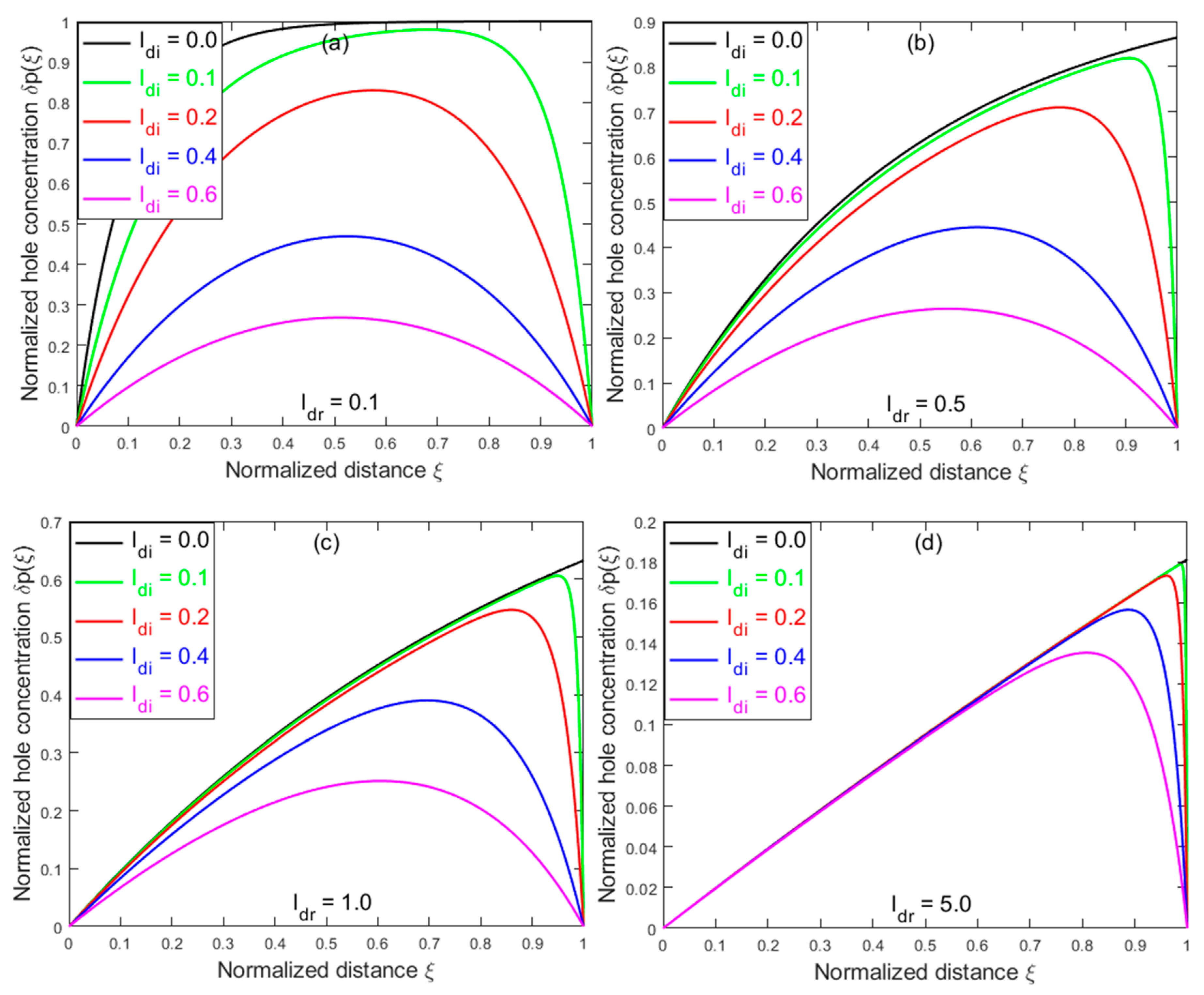
where , , [5,26]. The solution for electrons can be obtained by substituting with in Eq. (8). As , Eq. (8) recovers the drift-only result of Eq. (2) in [17]. Note that and depend only on two parameters: normalized drift length and normalized diffusion length , when expressed as normalized densities and , where is the normalized coordinate. Fig. 1 plots the normalized carrier density for Generally, is highly nonuniform and asymmetric in the photoconductive channel and it is more symmetric as diffusion becomes more dominant. Evidently, only in the low-drift and low-diffusion case (e.g., in Fig. 1(a)), (i.e., ) on the cathode side. This is in stark contrast to the common assumption of , which leads to highly questionable Eq. (1).
Figure 1.
Normalized spatial distributions of photogenerated holes for different combinations of diffusion and drift parameters, : (a) ; (b) ; (c) ; and (d) .
Figure 1.
Normalized spatial distributions of photogenerated holes for different combinations of diffusion and drift parameters, : (a) ; (b) ; (c) ; and (d) .
After being normalized to the maximum photocurrent and by introducing normalized coefficients, and , the photocurrent density of the holes can be calculated by using Eq. (7b) as given below
where is the drift current with diffusion, whilst is the diffusion current with drift. As , it recovers the drift-only result in : [19]. Again, the electron photocurrent density can be obtained by substituting with in Eq. (9). Both and are in general highly nonuniform. Fig. 2 plots using the same parameters (without ) as in Fig. 1.
Figure 2.
Normalized spatial dependencies of hole photocurrent densities for different combinations of diffusion and drift parameters, : (a) ; (b) ; (c) ; and (d) .
Figure 2.
Normalized spatial dependencies of hole photocurrent densities for different combinations of diffusion and drift parameters, : (a) ; (b) ; (c) ; and (d) .
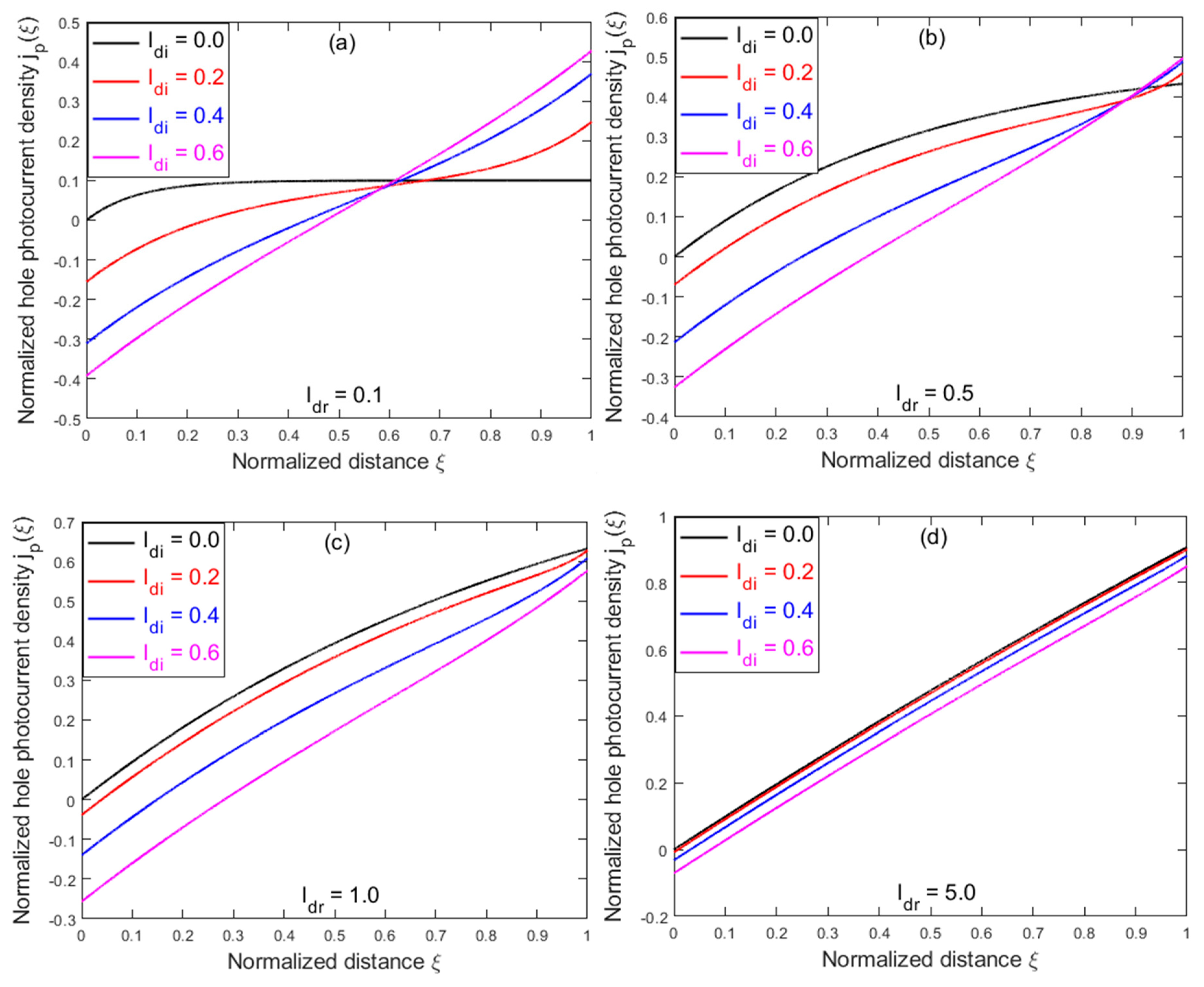
Due to the bidirectional nature of the carrier diffusion, a diffusion typically results in reduction in the net photocurrent. As shown in Fig. 2(a), with a fixed while increasing , at the anode decreases (becoming more negative), whereas at the cathode increases. For a small and large (e.g., and in Fig. 2(a)), is close to be anti-symmetric with respect to the center, thus, the average photocurrent is expected to be small (exactly zero for ), as expected for the diffusion dominating case. However, the diffusion effect is being suppressed with increasing drift length , i.e., for a fixed , increases with increasing from Fig. 2(a) to Fig. 2(d). For a large and small (e.g., .0 and in Fig. 2(d)), is positive in almost whole channel and approaches unity at , as expected for the drift-only case.
The total normalized photocurrent density, , including the contributions of both electrons and holes, can be calculated as
with the drift term
and the diffusion term . The photocurrent density, or , at the anode or cathode, respectively, represents the actual photocurrent that goes through the external circuit and can be directly measured. A short-circuit condition is implicitly assumed in the calculation. Thus, or more generally is expected, as indeed yielded by Eq. (10), which further constrains the selection of the BCs at the electrodes.
We then calculate as given below
where and . Note that Eq. (10) yields , as a direct result of adopting vanishing BCs. Thus, . Although Eq. (11) is from the “diffusion part” of Eq. (6b) or in Eq. (10), it recovers the result of drift-only current given by Eq. (3) when . When , can be expanded to the first order in
When and , , the same as Eq. (1a). As , , as does Eq. (3). By calculating the spatially averaged photocurrent density, we obtain the for holes
Note that the spatial average of the “diffusion term” in Eq. (6b) is identically zero for any and ; thus, only the “drift term” contributes to the photocurrent. For , becomes Eq. (4); when , and when , . The total is given by , which is simply or , when and . Thus, also has a unity limit. For a finite , when , can be expanded to the first order in , yielding
This result is consistent with [3], where the zero-field carrier density distribution is used for the calculation. When and , , consistent with Eq. (1b).
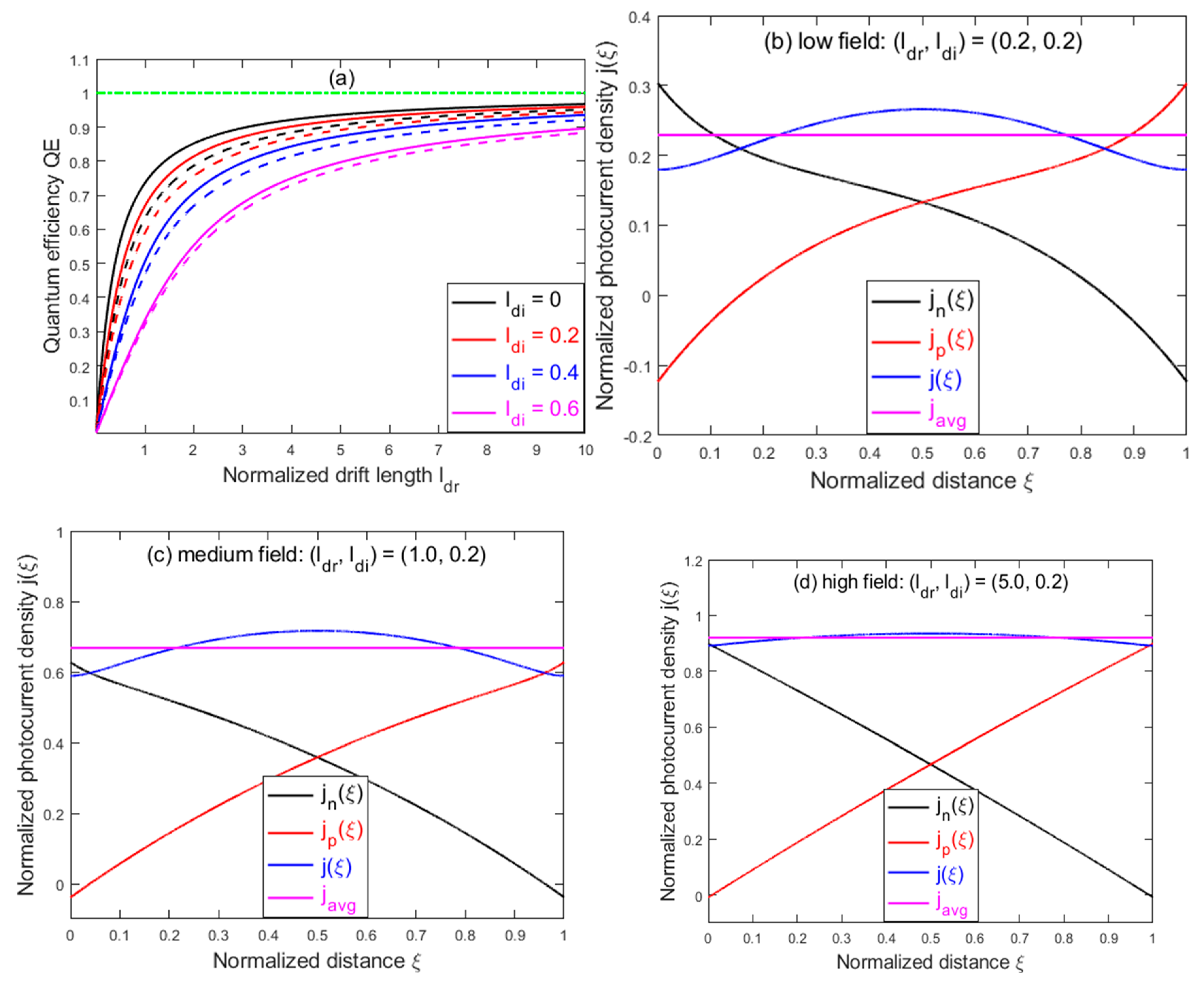
Fig. 3(a) plots and vs. for , and , showing in general. Both approach the unity limit as , which is true even as , as also shown in Fig. 3(a). In the limit of and , , whereas . Here, a factor of 2 difference is because of , but or and , whereas both and are averaged to . On the other hand, in the limit of , and , whilst and , i.e., at each electrode only one type of carrier contributes to the photocurrent, which contradicts the commonly accepted Eq. (1b), where both, the electrons and holes contribute to the photocurrent at each electrode. The situation is like the short circuit current calculation in a solar cell, where only one type of carrier is considered, even though a uniform carrier distribution is assumed [29]. It can be also seen from Fig. 3(a) that the diffusion effect, which results in bidirectional motion of the carriers, tends to reduce the photocurrent, compared to the drift-only case where the carrier motion is unidirectional under the applied field. Figs. 3(b)–(d) compare , , and with the spatially averaged value (equivalent to ) for three representative () combinations: low field , medium field , and high field , respectively, and illustrate how each type of carrier contributes to the total photocurrent at different field strengths measured by . When diffusion is significant, as in Fig. 3(b), and tend to have opposite signs and partially cancel each other at the electrodes, yielding a smaller net photocurrent. However, when drift is dominant, as in Fig. 3(d), one of and diminishes at the respective electrode, yielding a larger net photocurrent, approaching . Physically, the cancellation of the and can be understood as that some electrons reaching the anode may go back to the valence band directly, instead of flowing through the external circuit, which is equivalent to saying that some holes diffuse out from the anode. In the case with diminished diffusion, , no empty state in the valance band is available for the electrons to fill. Thus, the whole electron current flows through the external circuit and is the total current at the anode.
Interestingly, under the commonly adopted assumption of constant lifetimes, the total photocurrent is typically nonuniform, as shown in Figs. 3(b)-(d). The spatial modulation is more prominent in the case of low field or a small as shown in Fig. 3(b), but as the applied field increases, , as shown in Fig. 3(d). This spatial nonuniformity of the current is inconsistent with the conventional wisdom that the current should be constant throughout the circuit under continuous and uniform illumination [30]. However, from Eq. (6) and Eq. (7), one finds . The inhomogeneity decreases with increasing , since the significance of the recombination term diminishes. Fundamentally, this current inhomogeneity is caused by the deficiency of the constant carrier lifetime assumption for describing the carrier recombination. More generally, we should expect that , since in steady state, condition is required. This equality is obvious for the inter-band radiative recombination, usually expressed as , where is the radiative recombination coefficient. For the recombination through trap states, Shockley-Read-Hall (SRH) model [31,32] automatically ensures the equality. If is enforced in the drift-diffusion equations, we expect the two definitions to be equivalent. Other non-desirable effects of the constant carrier lifetime approximation have also been discussed in the past [30]. Thus, a more comprehensive model should be developed to eliminate this deficiency, as shown as necessary for other problems [33,34]. However, the drift-diffusion equations become nonlinear where analytic solutions are not obtainable and even numerical solutions are much more challenging [30].
Figure 3.
(a) Quantum efficiencies (dashed lines) and (solid lines) vs. drift length for different values, whilst the green line represents the maximum quantum efficiency . The total normalized photocurrent density , electron component , and hole component vs. normalized distance , compared to the spatially average photocurrent density for three different () combinations: (b) low field ; (c) medium field ; and (d) high field .
3. Numerical Solutions
To obtain the analytic solutions of drift-diffusion equations, we have assumed . When applying the commonly adopted vanishing BCs within the constant-lifetime approximation, we have further assumed and , to yield physically meaningful results. Here, we use numerical approaches to discuss the impacts of these approximations.
We first address the polarization effect, caused by the relative displacement of the electron and hole distributions, i.e., and induced by the applied field . The polarization effect is expected to be strong for small (corresponding to a large value) and values. Either a large or diminishes the excess carrier densities in the channel, thus, the polarization field. If the total field is written as , the change in the field can be expressed in terms of a potential through Besides the term, also affects the drift term, changing to , where is the drift length determined solely by . By defining with , one can write with . Eq. (7) can be then modified as given below
,
where and are, respectively, the drift lengths for electrons and holes determined solely by the external applied field, whilst or indicates the absence or presence of the polarization effect, respectively.
Solving the coupled nonlinear equations numerically is challenging for an arbitrarily small . Here, the goal is to qualitatively understand the potential impact of the polarization effect. For a not-too-small (e.g., ), Eq. (15) can be solved numerically for using an iterative method developed in this work. For simplicity, we still adopt and , while applying the same BCs: and . Explicitly, by setting , we first obtain the 0-th order carrier concentrations and , by solving Eqs. (15a) and (15b), then use the results in Eq. (15c) to solve for the 0-th order potential ; next, using , and setting , to solve for and . This process is repeated until the results converge (typically within 10 iterations).
The photocurrents at i-th iteration are evaluated as
Fig. 4 illustrates the impact of the polarization effect on different quantities, assuming , (e.g., a possible combination of a moderately high excitation condition: , , and ), for and after 10 iterations. Fig. 4(a) compares and , showing that the polarization effect makes the excess carrier distribution more uniform near the central region due to the depolarization field. Fig. 4(b) compares and , showing reduced current near the central region, while increased toward the two electrodes. Reducing from 0.5 to 0.1 leads to the stronger polarization effect, but the impact is relatively small: an increase in from 0.196 to 0.206 and decrease in from 0.289 to 0. 276, as shown in Figs. 4(c) and 4(d), respectively.
Figure 4.
Impact of polarization effect on the excess carrier distributions and photocurrent density: (a) normalized carrier distributions and vs. normalized distance ; (b) normalized spatial photocurrent densities and vs. normalized distance ; (c) quantum efficiency vs. normalized Debye length ; and (d) quantum efficiency vs. normalized Debye length .

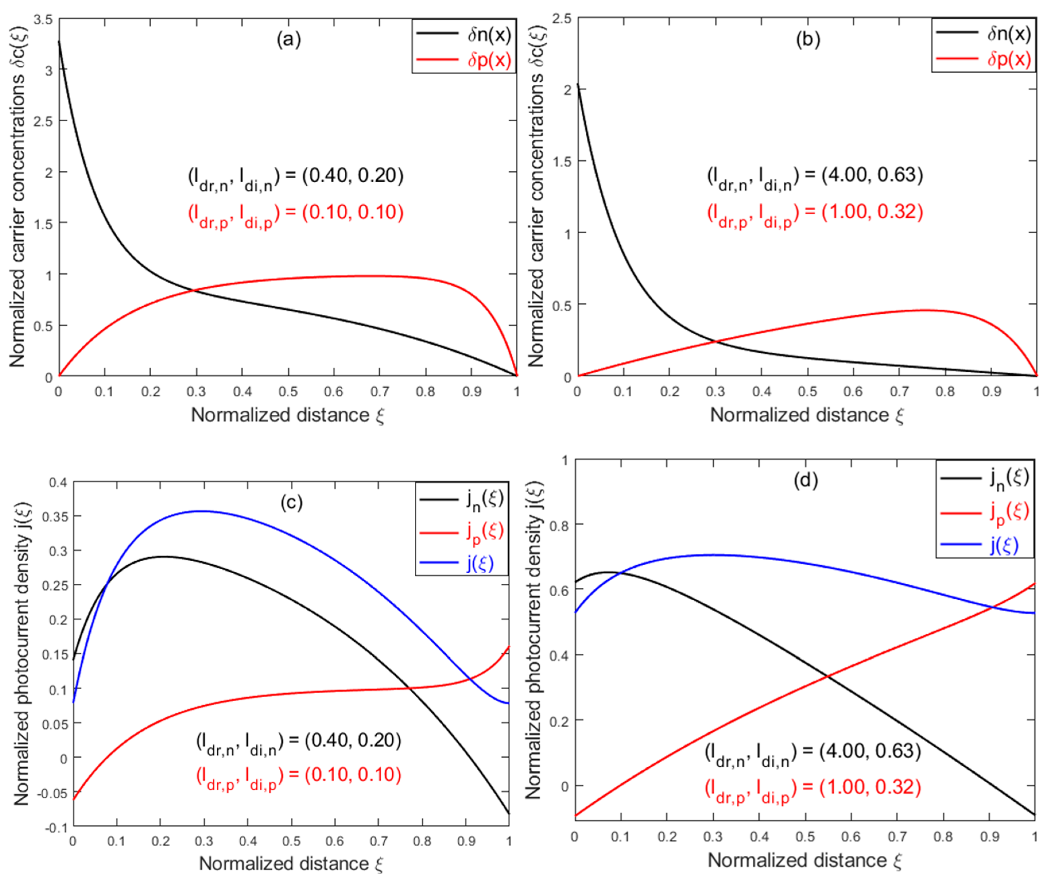
We next examine the possible impacts of non-equality in the mobility-lifetime product of electrons and holes. We assume but and neglect the polarization effect (). For the case of and , the charge neutrality condition is satisfied automatically. However, assuming , solving Eq. (7) under the same BCs of would result in and , which violates the current continuity and charge neutrality conditions.
The physical explanation is that when electrons coming out of the anode cannot be accepted by the cathode at the same rate when , an accumulation of electrons will occur at the boundary with the anode. From , one can see that if is satisfied, will automatically be satisfied as well. Therefore, we need to find that can satisfy . One possible solution is to allow , whilst other BCs are kept unchanged. Although an analytical solution can still be obtained, it is too complex to be shown here. Thus, only numerical results for are given to illustrate the effects. Figs. 5(a) and (b) plot the carrier distributions of electrons and hole, and , respectively, for two different combinations of and . Figs. 5(c) and (d) plot , and , respectively, for the same set of parameters. As expected, with increasing drift and diffusion parameters, both components tend to become linear; thus, the total photocurrent tends to become uniform.
Figure 5.
Normalized carrier distributions and photocurrent densities: (a) Normalized electron distributions vs. normalized distance ; (b) Normalized hole distributions vs. normalized distance ; (c) and (d) Total normalized photocurrent density , the electron component and the hole component vs. normalized distance .
4. Simulation Results
To examine how our analytic model compares to a commonly available device simulator, we perform numerical simulations using “Drift-Diffusion Lab” from nanoHub.org [35]. Note that this simulation tool also assumes constant carrier lifetimes, but considers the field dependent mobilities, i.e., , as well as spatially dependent electric field, i.e.,
Firstly, by letting and , we compare the potential differences in the carrier distributions. Germanium (Ge) is selected as the active material with following parameters: , , , , , and surface recombination velocity at the electrodes , the largest allowed value in the simulator. Although is meant to be the surface recombination velocity, we take it as the carrier extraction velocity that is assumed to be infinity in the analytic model. Fig. 6(a) plots and with . The simulation results (solid curves) are compared to those obtained from the analytic model (dashed curves). As shown in the figures, for a small applied voltage (e.g., V or ), the simulation results are significantly different from those of the analytic model, but the difference diminishes for larger applied voltages (e.g., V or ).
Secondly, we examine the effect of polarization on the J-V characteristics. For the same parameters, Fig. 6(b) plots the J-V curves of the simulated results (black solid curve) and compares them with the analytic results: (red solid curve) and (blue solid curve). We find , but they all approach the unity limit for the strong drift.
Thirdly, we examine the differences in the spatial variation of the photocurrent. By using the simulated carrier densities from Fig. 6(a), we calculate the spatial variations of the photocurrents by using Eq. (7), in which the electric field is obtained by integrating Eq. (7c), while keeping same voltage difference between the electrodes as the applied voltage. The results are shown in Fig. 6(c) and 6(d) (solid curves), in comparison with the results of the analytic model (dashed curves) for: 0.1 V, 1.0 V and 2.0 V. Due to the singularity in taking derivative using the numerical data, out of 150 data points, the last two data points closest to the respective electrode are found unreliable, and, thus, they have been omitted in the plots. However, the extrapolated values at the electrodes are close to the direct current outputs of the simulations. Thus, the values of the simulation current are used for the end points at and . Clearly, the total current remains nonuniform, with a maximum at the center, with comparable modulation amplitudes compared to the analytic results. Ratios between the maximum and minimum points are found to be 1.611, 1.205, and 1.108, from the analytic results, compared to 1.382, 1.099, and 1.050 from the simulation results, for 0.1 V, 1.0 V, and 2.0 V, respectively and the photocurrents become more uniform under a larger applied electric field. Beside the systematically larger compared to that of the analytic model , the simulated results show upward bending near the end points.
Figure 6.
Comparison of the simulation results and analytic results: (a) Electron distributions and hole distributions for 0.1 V and 1.0 V; (b) The simulated photocurrent density and analytic photocurrent densities and vs. applied voltage; (c) and (d) Spatial dependences of the simulated photocurrent density and analytic photocurrent density for 0.1 V, 1.0 V and 2.0 V. The green lines represent the maximum photocurrent density .
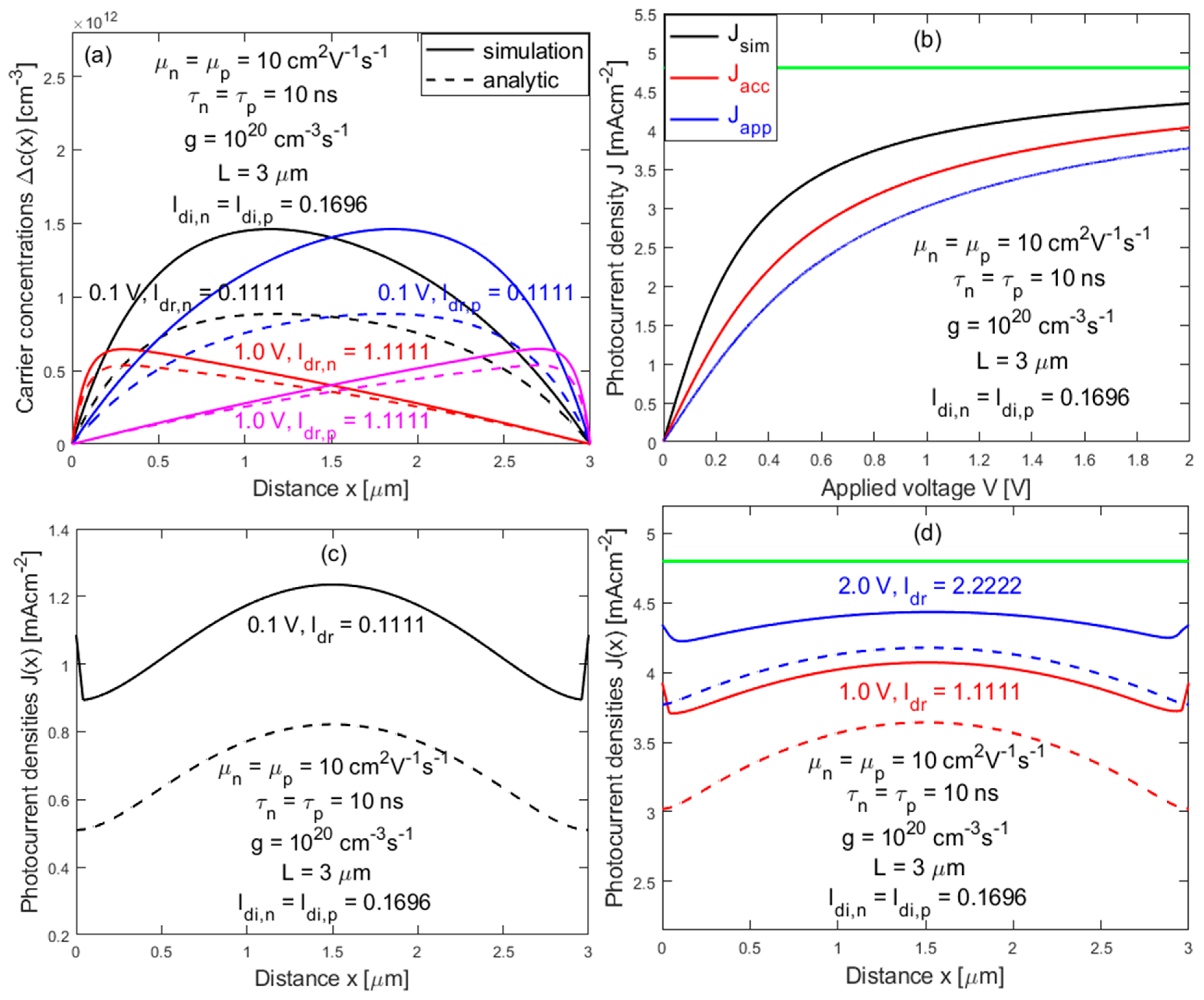
Furthermore, we would like to point out that the differences between analytic and simulation results are not simply due to whether the polarization effect is included or not. In fact, according to our numerical simulation results as described in the previous section, the polarization effect is expected to be minimal for . However, the simulator considers other effects, such as the carrier density and field dependences of mobility. Therefore, even using the same mobility and lifetime parameters for the electrons and holes, the relationship of , predicted by the analytic model, is often found invalid for the simulated results. Consequently, we found that the charge neutrality condition, i.e., , does not always hold true in the simulated results. However, we have made a concerted effort to identify the parameters, which ensures that the charge neutrality condition in the photoconductive channel is nearly satisfied, as shown in Fig. 6(a). Overall, the numerical simulations, which include the polarization effect and beyond, do not result in qualitative differences from the analytic model, but do exhibit significant quantitative differences, particularly for the cases of small values, for instance, in Figs. 6(a) and (c) when
5. Discussion
There are various possible secondary photoconductive effects, such as the carrier injection from the electrode, caused by either thermal injection (i.e., space-charge limited current or SCLC) [1] or light induced changes in the M-S interface [36], carrier recycling or replenishing [1,4,13,17,37], and other mechanisms [27,38]. Often, photoconductive devices involve doped semiconductors [3,5]. In fact, doping or substantial intrinsic carrier density in the photoconductive channel bears some similarity with the SCLC effect, except that the charges that induce the dark current are provided internally for the former and injected from the electrode for the latter. In both cases, the presence of the pre-existing charges may alter the distributions of the photogenerated carriers, thus, the quantum yield. However, including any of these secondary photoconductive effects makes it impractical to obtain rigorous analytic solutions for the photocarrier distributions and photocurrent. Nevertheless, various approximate formulae have been given for different situations [16,37,39,40]. Furthermore, for a doped device and under the ambipolar-transport approximation, the gain limit has been found to be , where is the ratio of majority to minority carrier mobilities [3,16]. This formula indicates that a modest gain above unity is possible, as verified by numerical simulations [5]. When the equilibrium carrier densities are much greater than the excess carrier densities and and when the ambipolar diffusion length is much smaller than the channel length, a gain formula equivalent to Eq. (1b) is obtained for an intrinsic device, suggesting that quantum yields far exceeding unity are possible [16].
However, as confirmed analytically and by simulations in this work, if only the primary photoconductivity is considered, the undoped photoconductive devices with minimal equilibrium carrier densities cannot have or above unity, independently of the values of the device parameters. The widely used gain formula given by Eq. (1) appears to be the low-field-limit result of Eqs. (11) and (13), when the effect of diffusion is neglected. Secondary photoconductive mechanisms are indeed required to understand many experimental reports of the greater-than-unity gains. However, for various possible secondary photoconductivity mechanisms, the simplified form of photoconductive gain given by Eq. (1) is unlikely to remain valid in general. Extending the current work to include secondary photoconductive mechanisms will be the subject of our future work.
6. Summary and Conclusions
By assuming primary photoconductivity, perfect carrier extraction, constant parameters of carrier lifetimes and mobilities, negligible thermally generated carriers and negligible polarization effect, an analytic model with arbitrary strength of diffusion and drift for a photoconductive device with an intrinsic semiconductor has been provided. Numerical simulations have been performed to confirm the conclusions of the analytic model. We have shown that: (1) while the general theory is capable of recovering the drift-only results in the early literature, the photoconductive gain remains limited to unity; (2) the commonly adopted photoconductive gain formula as the ratio of the lifetime τ to the transit time is only valid in the low-drift length region, when the effect of diffusion is neglected; (3) when solving the drift-diffusion equations a proper care should be taken in selecting BCs to ensure equality of photocurrents at both electrodes; (4) the impact of neglecting the polarization effect, due to the relative displacement of the excess electrons and holes, is relatively small; and (5) the non-equivalency of the definitions, i.e., , is the deficiency of the commonly adopted constant-carrier-lifetime approximation, which also leads to the nonuniform photocurrent in the channel. The insights of this work should help in reexamination of the photoconductive gain theories involving doped semiconductors and/or other secondary photoconductive effects. Thus, it lays the ground for understanding the mechanisms of the experimentally observed above-unity photoconductivity gains.
Acknowledgments
The work was supported by U.S. DoD grant W911NF-23-1-0215 and Bissell Distinguished Professor endowment fund at UNC-Charlotte. We thank Prof. Dragica Vasileska and Prof. Gerhard Klimeck for helpful discussions about using “Drift-Diffusion Lab” from nanoHUB.org.
Appendix
Hecht [19] and Mott-Gurney [1] derived quantum efficiency by considering that for the carriers that either can or cannot reach the electrode, their contributions to the photocurrent are given by their travel lengths toward the collecting electrode in ratio to the channel length. In this consideration, if electrons are generated at a distance from the anode and their number decays while they are drifting toward the electrode under a bias, the number of the electrons that do not reach the electrode weighted by the fraction of the travel distance is given as
whereas the number of the electrons that do reach the electrode weighted by the fraction of the travel distance is given as
The effective total number of electrons, , that contribute to the photocurrent is given by
On the other hand, Rittner [16] and Many [17] used the average carrier density in the channel, , to calculate the photocurrent:
By noticing that , one can see that these two approaches are equivalent, i.e., .
References
- N. F. Mott and R. W. Gurney, “Electronic Processes in Ionic Crystals”, Oxford: Oxford University Press (1940).
- R. H. Bube, “Photoconductivity of Solids”, John Wiley & Sons, Inc. (1960).
- H. Beneking, IEEE Transactions on Electron Devices, Vol. 29 Issue 9, 1431-1441 (1982). [CrossRef]
- R. S. Quimby, “Photonics and Lasers-An Introduction”, John Wiley & Sons, Inc. (2006). [CrossRef]
- Y. Dan, X. Zhao, K. Chen, and A. Mesli, ACS Photonics, Vol. 5, No. 10, 4111-4116 (2018). [CrossRef]
- W. Smith, Nature volume 7, 303 (1873). [CrossRef]
- R. W. Smith, RCA Rev. 12:350-361 (1951).
- C. Soci, A. Zhang, X. Y. Bao, H. Kim, Y. Lo, and D. Wang, Journal of Nanoscience and Nanotechnology, Vol. 10, No. 3, 1430-1449 (2007). [CrossRef]
- R. Dong, Y. Fang, J. Chae, J. Dai, Z. Xiao, Q. Dong, Y. Yuan, A. Centrone, X. C. Zeng, and J. Huang, Adv. Mater. 27, 1912-1918 (2015). [CrossRef]
- Q. Guo, A. Pospischil, M. Bhuiyan, H. Jiang, H. Tian, D. Farmer, B. Deng, C. Li, S. J. Han, H. Wang, Q. Xia, T. P. Ma, T. Mueller, and F. Xia, Nano Lett., 16, 4648-4655 (2016). [CrossRef]
- A. Rose, RCA Rev. 12:362-414 (1951).
- S. M. Sze and K. K. Ng, “Physics of Semiconductor Devices”, 3rd ed.; John Wiley & Sons, Inc. (2007). http://doi.org/10.1002/0470068329.
- D. A. Neamen, “Semiconductor Physics and Devices: Basic Principles”, 4th ed.; McGraw-Hill (2012).
- M. Grundmann, “The Physics of Semiconductors-An Introduction Including Nanophysics and Applications”, 4th ed.; Springer (2021). http://doi.org/10.1007/978-3-030-51569-0.
- O. Lopez-Sanchez, D. Lembke, M. Kayci, A. Radenovic, and A. Kis, Nature Nanotechnology 8, 497−501 (2013). [CrossRef]
- E. S. Rittner and R. G. Breekenridge, Ed., B. R. Russell, in Photoconductivity Conference. 215-268, New York: Wiley (1956).
- A. Many, Elsevier, J. Phys. Chem. Solids Pergamon Press, Vol. 26, 575-585 (1965). [CrossRef]
- B. Gudden and R. Pohl, Springer, Zeitschrift für Physik, 17, 331-346 (1923). [CrossRef]
- K. Hecht, Springer, Zeitschrift für Physik, 77, 235-245 (1932). https://link.springer.com/article/10.1007/bf01338917.
- R. Hilsch, R. W. Pohl, and H. L. Jackson, Transactions of the Faraday Society 34, 883-888 (1938). https://pubs.rsc.org/en/content/articlepdf/1938/tf/tf9383400883.
- R. S. van Heyningen and F. C. Brown, Phys. Rev., Vol. 111, No. 2, 462-471 (1958). [CrossRef]
- J. K. Marmon, S. C. Rai, K. Wang, W. Zhou, Y. Zhang, Front. Phys., Sec. Optics and Photonics, Vol. 4 (2016). [CrossRef]
- Y. Zhang, J. K. Marmon, “Light-Effect Transistor (LET)”, US 20170104312 A1, The University of North Carolina at Charlotte (2017).
- W. van Roosbroeck, Phys. Rev., Vol. 91, No. 2, 282-289, (1953). [CrossRef]
- P. J. van Heerden, Phys. Rev., Vol. 106, No. 3, 468-473, (1957). [CrossRef]
- C. H. Chu, M. H. Mao, C. W. Yang and H. H. Lin, Scientific Reports 9, Article number: 9426 (2019). [CrossRef]
- M. Karimi, X. Zeng, B. Witzigmann, L. Samuelson, M. T. Borgström, and H. Pettersson, Nano Lett. 19, 8424-8430 (2019). [CrossRef]
- R. H. Bube, “Photoelectronic Properties of Semiconductors”, Cambridge University Press. (1992).
- W. Shockley and H. J. Queisser, Journal of Applied Physics, Vol. 32, No. 3, 510-519 (1961). [CrossRef]
- M. Hack and M. Shur, J. Appl. Phys. 58 (2) (1985). http://dx.doi.org/10.1063/1.336148.
- R. N. Hall, Phys. Rev., Vol. 87, 387 (1952). [CrossRef]
- W. Shockley and W. T. Read, Phys. Rev., Vol. 87, No. 5, 835-842, (1952). [CrossRef]
- F. Zhang, J. F. Castaneda, T. H. Gfroerer, D. Friedman, Y. H. Zhang, M. W. Wanlass, and Y. Zhang, Nature, Light: Science & Applications 11, Article Number: 137 (2022). [CrossRef]
- J. He, K. Chen, C. Huang, X. Wang, Y. He, and Y. Dan, ACS Nano, 14, 3405-3413 (2020). [CrossRef]
- S. R. Mehrotra, A. Paul, G. Klimeck, and G. W. Budiman, “Drift-Diffusion Lab”, (2021). [CrossRef]
- M. Hiramoto, T. Imahigashi, and M. Yokoyama, Appl. Phys. Lett. 64, 187-189 (1994). [CrossRef]
- R. Hilsch, R. W. Pohl, Springer, Zeitschrift für Physik, 108, 55-84 (1938). [CrossRef]
- R. L. Petritz, Phys. Rev. 104, 1508-1516 (1956). [CrossRef]
- R. W. Pohl and F. Stöckmann, Annalen der Physik, 6. Folge, Band 1, Heft 6, 275-284, (1947). [CrossRef]
- F. Stöckmann, Physica Status Solidi (a), Vol. 15, Issue2, 381-390, (1973). [CrossRef]
Disclaimer/Publisher’s Note: The statements, opinions and data contained in all publications are solely those of the individual author(s) and contributor(s) and not of MDPI and/or the editor(s). MDPI and/or the editor(s) disclaim responsibility for any injury to people or property resulting from any ideas, methods, instructions or products referred to in the content. |
© 2025 by the authors. Licensee MDPI, Basel, Switzerland. This article is an open access article distributed under the terms and conditions of the Creative Commons Attribution (CC BY) license (http://creativecommons.org/licenses/by/4.0/).
Copyright: This open access article is published under a Creative Commons CC BY 4.0 license, which permit the free download, distribution, and reuse, provided that the author and preprint are cited in any reuse.


