Submitted:
12 March 2025
Posted:
13 March 2025
You are already at the latest version
Abstract
Until now, achieving both high spectral resolution on the order of a few wavenumbers and the highest sensitivity in Raman scattering spectroscopy required reliance on high-end laboratory instruments. Here, we introduce an innovative yet design-wise simple alternative: a cost-effective and compact micro-Raman spectrometer (µRS) that combines exceptional spectral resolution and sensitivity. Leveraging industrial-grade CMOS cameras and high-quality photographic objectives, our µRS maintains a footprint at least five times smaller than traditional lab-based spectrometers. Through detailed characterization and direct experimental comparison, which includes the use of calcite as a Raman standard, we demonstrate that our µRS achieves spectral resolution of down to 2.5 cm-1. Using single-layer MoS2 sample we found sensitivity comparable to commercial research-grade confocal Raman microscopy systems. This study presents a compelling solution for researchers seeking efficient and high-resolution Raman spectroscopy tools across diverse applications, particularly in resource-limited or field-based settings.
Keywords:
raman spectrometer
; cost-effective
; compact spectrometer
1. Introduction
Raman spectrometers have become essential equipment not only in research laboratories but also in industrial settings. Portable versions of these instruments enable reliable in situ and on-site analysis of many (bio)chemicals, finding applications in fields such as forensic science, pharmaceuticals, healthcare, agriculture, and environmental monitoring.
Depending on the specific need and application, there is a wide range of Raman spectrometers to choose from. Among the most common types found in research labs are Research Grade Raman Spectrometers (RGRSs) and Fiber Raman Spectrometers (FRSs).
FRSs are compact, robust, and relatively immune to stray light and external noise, making them ideal for in-field measurements and portable applications. However, their design prioritizes ease of use and mobility over high spectral performance. Research-grade Raman spectrometers RGRSs, on the other hand, offer higher spectral resolution and sensitivity but are significantly more expensive—often costing several times more than FRSs—and are typically limited to benchtop formats, restricting their use to laboratory environments.FRSs generally provide a spectral resolution in the 4–10 cm⁻¹ range, which is sufficient for quick, non-destructive identification of chemical composition. However, for applications requiring higher spectral resolution, such as distinguishing subtle peak shifts in solid-state physics or monitoring closely spaced vibrational modes, more advanced instrumentation is required. This need motivated us to develop a compact micro-Raman spectrometer (µRS) from scratch, aiming to bridge the gap between FRS portability and RGRS performance.
The result is a system that costs an order of magnitude less than a typical lab-grade Raman spectrometer while delivering comparable spectral resolution and sensitivity. A detailed cost comparison is provided in Section 1 in SM: Table S1-2 and Table S1-3, highlighting the affordability of µRS.
High spectral resolution (i. e. <4 cm-1) and high sensitivity, up to know achievable only with RGRSs, are essential requirements for many Raman spectroscopy applications. For instance, high spectral resolution on the order of few wavenumbers is needed to monitor tiny changes in the Raman shift and linewidth of a Raman band, which provides insights into the local environment of a vibrating group. This is crucial for the development and research of low-dimensional materials such as monolayer MoS2 [1], to identify crystallinity [2,3], polymorphism [4,5], intrinsic stress or strain in solid state matter [6], hydrogen bonding [7] and protein folding in soft matter [8].
Achieving high-sensitivity is equally important, as Raman scattering has a cross-section that is 10-12 orders of magnitude smaller than that of molecular absorption [9]. Thus, every photon is important, and a high-sensitivity spectrometer is necessary to obtain a sufficiently high signal-to-noise ratio (SNR) for low-light conditions. This is achieved through the combination of a high-throughput optical bench and a photon detectors having low dark noise (DN) and high quantum efficiency (Qe) at the wavelengths of interest. More precisely, to get a good SNR the detector needs to have Qe over DN ratio (Qe/DN) as high as possible at wavelengths of interes [10]. Let’s first consider the optical bench throughput (OBT) contribution.
RGRSs simultaneously offer high spectral resolution of <4 cm-1 and highest sensitivity available on the market. Surprisingly, OBT of a general purpose RGRS is sometimes lower than 40% [11,12]. As this type of Raman spectrometers are designed with excitation wavelength versatility and simplicity of use in mind, usually the same optical elements need to handle wavelengths spanning from the ultraviolet to the near infrared region (NIR). However, broadband performance comes at the expense of OBT. Therefore, we decided to limit our spectrometer’s spectral range to the visible region (VIS) where optical elements are abundant and come with a reasonable price tag.
Instead of mirrors or simple lenses we have chosen general purpose photographic objectives. That was motivated by three reasons: they have high transmittance of >95% throughout the whole VIS region, they are corrected for all major optical aberrations and their cost is comparable to the cost of a simple achromatic lens at an optics laboratory supplier. By opting for lens-based design the optical grating reflectance becomes the limiting factor of OBT. The only drawback is that the excitation wavelength is now limited to VIS, but this is acceptable for many applications. Extension to the shorter end of NIR (780-1050 nm), a spectral range that covers popular Raman excitation at 785 nm and that is still detectable with a low-cost silicon-based camera, is easily implemented simply by switching to grating and lenses optimized for this spectral region.
With the emergence of newer technology, particularly CMOS sensors, which are widely implemented in high-volume consumer electronics such as cell phones, CMOS imaging sensors have rapidly gained popularity in industrial, large-scale, and cost-effective research applications (Fossum, 2020). These sensors have evolved to offer low DN and high Qe, making them a viable alternative to more expensive scientific-grade detectors. To achieve optimal sensitivity while minimizing costs, we selected two industrial-grade CMOS cameras (iCMOS), which provide a low read noise of 2–3 e⁻/pixel, quantum efficiency (Qe) greater than 60%, and low dark current even without cooling (FLIR, 2023). These cameras offer a cost roughly one-tenth that of scientific-grade CCD or CMOS cameras, making them an attractive choice for high-performance yet affordable Raman spectroscopy.
We employ two different iCMOS cameras not only because they have different pixel pitches but also to investigate whether spectral resolution is limited by the pixel broadening effect. By comparing the two detectors, we aim to determine whether decreasing spectral dispersion per pixel leads to a tangible improvement in spectral resolution or whether the limiting factor lies elsewhere in the optical system. This dual-camera approach ensures a balance between cost, sensitivity, and spectral performance, making it a practical solution for high-resolution Raman spectroscopy.
Ma and coworkers compared an scientific CMOS (sCMOS) camera with an iCMOS camera (based on the IMX265 sensor, the same one as in CAM-L - the 3.45 µm pixel camera) and found that the SNR in low light conditions is comparable and that the iCMOS camera even outperforms Electron-Multiplying CCDs (EMCCDs) for signals above 20 photons/pixel [13]. As a rule of thumb, for exposure times less than a few seconds, iCMOS cameras offer comparable performance to cooled sCMOS and sCCD cameras in terms of negligible dark current noise contribution, and they do not require cooling [10,14,15]. Our primary motivation for building the µRS is to create a workhorse for confocal Raman mapping, an experimental technique that commonly uses exposure of less than 1 s. Therefore, it is reasonable to assume that for our experimental conditions, the dark noise of the CMOS camera is mainly due to the read noise, while contribution of the dark current noise is negligible. Our experience show that even longer exposures of 10-20 s give good results.
The aim of this paper is to demonstrate that a low-cost µRS can be constructed using commercial off-the-shelf (COTS) components, including photographic lenses, iCMOS cameras, and other widely available optical elements. Despite its simple and cost-effective design, our homebuilt Raman spectrometer achieves a high spectral resolution of 2.6–3 cm⁻¹ and sensitivity comparable to research-grade Raman spectrometers (RGRSs). However, unlike RGRSs, which are typically expensive and limited to laboratory settings, our µRS is built at a cost one order of magnitude lower, making high-resolution Raman spectroscopy more accessible for various research and industrial applications.
2. Micro-Raman Spectrometer Construction
A schematic of the µRS setup, illustrating all optical components along the beam path—from the excitation laser to the detector—is presented in Figure 1. The system consists of two main parts: the Raman probe, which focuses the 532 nm laser onto the sample, collects the Raman-scattered photons, and directs them to the entrance slit of the high-resolution spectrometer; and the lens-based dispersive spectrometer, which utilizes an iCMOS camera as the detector.
To accommodate different experimental needs, we incorporate two interchangeable cameras with different pixel pitches: one with larger 3.45 µm pixels (µRS -3.45) and another with smaller 1.85 µm pixels (µRS -1.85). The µRS-3.45 configuration is optimized for higher sensitivity, making it ideal for low-light conditions, while the µRS -1.85 configuration offers higher spectral resolution, providing finer detail in Raman peak structures. Switching between the two cameras is straightforward, allowing flexibility based on the specific demands of the measurement. A general overview of the device is provided here, while detailed specifications, including exact part numbers and component choices, are given in Section 1 in Supplementary Material (SM).
Micro-Raman Probe
For the excitation laser L (Figure 1), we selected a single longitudinal mode (SLM) diode-pumped solid-state (DPSS) laser operating at 532.13 nm. The laser spectrum and its linewidth ( = 0.4 cm⁻¹) were characterized using an optical spectrum analyzer (OSA) in high-resolution mode (Section 2 in SM: Fig. S2-1).
In Raman spectroscopy, the natural linewidth Γ of a Raman peak is affected by both the spectrometer’s spectral resolution and the laser linewidth . The experimentally measured linewidth represents a convolution of these broadening effects. However, since of the µRS is, as we will see in the following, at least five times broader than , the contribution of to is negligible in our measurements.
The excitation beam first passes through the beam expander BE, where it is expanded fivefold before being reflected by the folding mirror M. It then reaches the Raman filter FR, which suppresses Rayleigh scattering while also serving a second purpose: when tilted by 5°, it allows the excitation beam to be inserted along the LOBJ-LCPL optical axis, ensuring collinearity between the excitation and Raman-scattered photons (RSP) beams. This dual-purpose design eliminates the need for a separate dichroic beamsplitter, simplifying the optical layout while also suppressing Rayleigh scattering. As a result, the system achieves higher throughput, reduced cost, and the possibility to upgrade the µRS so that it can access wavenumbers in the ultralow-frequency (ULF) region, down to 5 cm⁻¹ [16].
Upon reflection from FR, the excitation beam reaches the collection objective LOBJ, which focuses it onto the sample S mounted on the sample holder (Fig. S4-1, lower panel). We calculated the laser spot size and, consequently, the RSP spot size , as they originate from the same illuminated region. The final spot size is 0.31 µm (FWHM), as determined in Section 3 in SM. The choice of a microscope objective minimizes spherical aberration, ensuring optimal focusing and efficient collection of RSP across large collection angles, improving SNR. The collected RSP beam then passes through FR, enters the back aperture of the coupling objective LCPL, and is focused onto the center of the entrance slit SLT, which is 5 µm wide (Section 4 in SM: Fig. S4-1, lower panel), forming the RSP spot image at the slit plane. We denote the FWHM of this image as .
As we will see in the following, is one of the key parameters in determining the spectral resolution (Eq. 2). The details of calculation of are provided in Section 4 in SM. The approach accounts for diffraction effects but neglects optical aberrations, as these are well corrected in microscope objectives [17]. In brief, the Point Spread Function (PSF) of the optical system LOBJ-LCPL is modeled using the scalar Debye diffraction integral in non-paraxial imaging, which accurately describes near-focus light distribution even for high numerical aperture (NA) microscope objectives [18]. A Gaussian approximation is then applied to the obtained PSF [19]. The calculation yields that varies from 2.08 µm at = 0 cm⁻¹ to 2.23 µm at = 2000 cm⁻¹. Throughout this paper, we adopt the value of at = 1000 cm⁻¹, corresponding to the central region of the Raman spectrum, where it amounts to 2.15 µm.
High-Resolution Lens-Based Spectrometer
The spectrometer includes an entrance slit (SLT, Figure 1) with a width of 5 µm, which, in combination with approximately 10 pixel integration along the y-axis (the non-dispersive axis parallel to the slit height, see the coordinate system near CAM on Figure 1), forms a virtual confocal pinhole [20]. This setup enables a quasi-confocal regime, where the system selectively samples the Raman signal from the sample region near the focal plane of LOBJ. As a result, an optical sectioning effect is achieved [20].
After passing through the entrance slit, the RSP beam is collimated by a 50 mm photographic lens (the slit lens LSLT, Figure 1) and directed onto a holographic reflective diffraction grating (G) at an incidence angle of θi = 55°. The choice of a 50 mm photographic lens is both practical and cost-effective. As one of the most widely used focal lengths in photography for decades, these lenses are mass-produced, well-corrected for major aberrations in the visible range. In contrast, RGRSs typically use camera lenses with focal lengths of at least 250 mm, contributing to their bulkiness and large footprint. By using a shorter focal length, µRS achieves a fivefold reduction in size, making it significantly more compact while maintaining high optical performance.
For a central wavelength of 532.13 nm and a holographic reflective diffraction grating with 2400 lines/mm, the grating equation (Section 5 in SM: Eq. S5-1) yields m = -1 as the only possible diffraction order. The angle α = 27.5°, defined as the angle between the incident and diffracted rays (Section 5 in SM: Fig. S5-1), is chosen to minimize the spectrometer’s footprint. To simplify operation, the grating remains static, allowing the camera to acquire the entire Raman spectrum without mechanical adjustments. Consequently, the incident angle is fixed at =55° (Section 5 in SM: Eq. S5-7), a configuration commonly referred to as static grating mode (Liu and Berg, 2012). From , the diffraction angle (Section 5 in SM: Eq. S5-8) can be determined, followed by the maximum number of illuminated grooves on the grating and, ultimately, the smallest resolvable wavelength difference of the grating, calculated as ≈ 0.01 nm (Section 5 in SM: Eq. S5-11), or equivalently, ≈ 0.3 cm⁻¹.
However, as we will see, the actual spectral resolution is almost an order of magnitude larger. This significant degradation in resolution (where a larger indicates lower resolution) arises not from the grating’s groove spacing d but rather from the size of the RSP spot image at the detector , which becomes the dominant limiting factor.
For the detectors, we opted for two industrial-grade iCMOS cameras, CAM-L and CAM-S, with specifications detailed in Section 1 in SM: Table S1-1. Each camera offers distinct advantages depending on the measurement needs. CAM-L features a 3.45 µm pixel size, Qe of 62% at 530 nm, an exceptionally low read noise (RN) of 2.26 e⁻/pixel, and a low dark current of 0.8 e⁻/s [21]. Its Qe is only slightly lower than that of a typical sCMOS camera, while its RN is more than twice as low as in a cooled sCCD camera. Due to its low RN and dark current, this low-cost, uncooled iCMOS camera achieves a lower dark noise than a cooled sCCD camera, even with exposure times of several seconds.
In addition, we incorporated CAM-S, which has a smaller pixel size of 1.85 µm, a higher Qe of 73% at 530 nm, and a RN of 3.18 e⁻/pixel, with a dark current comparable to CAM-L. The motivation for including CAM-S is to investigate whether decreasing spectral dispersion per pixel (Section 6 in SM: Eq. S6-4) —commonly referred to as pixel resolution (cm⁻¹ per pixel) —offers an improvement in . Since spectral resolution is ultimately limited by the size of the RSP spot image at the detector, testing CAM-S allows us to evaluate whether finer pixel sampling provides a measurable performance benefit.
3. Calibration and Characterization
Calibration of the Raman Shift Axis
The calibration protocol for the micro-Raman spectrometer follows the same principles as in our previous work [22], with three key steps ensuring measurement precision. It relies on two reference standards: a neon spectral lamp and cyclohexane (cHex), an ASTM Raman reference standard [23]. The process involves monthly wavelength calibration using nine neon emission lines between 535 and 585 nm, daily laser wavelength measurement with cHex, and daily wavenumber fine-tuning with cHex before measuring the sample of interest.
Since Raman shifts are calculated relative to the excitation laser wavelength λL, accurately determining λL is crucial. Ambient fluctuations can cause λL to shift by ±2 cm⁻¹ monthly, but recalibration using cyclohexane allows for an accuracy of ±0.2 cm⁻¹. For further details on the Raman shift calibration protocol, including λL determination, Ref. (Zgrablić et al., 2025): Section 3 in SI can be consulted.
Spectral Resolution Characterization
To experimentally determine the spectral resolution of a spectrometer, we describe the lineshape of a Raman mode using a Voigt profile. A Raman peak with a well-established natural linewidth Γ from the literature is selected and fitted with a Voigt function, where the Lorentzian width ΓL is constrained to the reference value Γ. One of the fit parameters, the full width at half maximum (FWHM) of the Gaussian component ΓG, is taken as the experimental value of the spectral resolution at the Raman shift of the analyzed peak. By applying this procedure to multiple peaks, is characterized across different Raman shifts.
For spectral resolution characterization, we use a calcite crystal, which has three Raman peaks with well-established natural linewidths. The calcite sample, sourced from the calibration sample collection at the Institute of Physics in Zagreb, is a stable solid with no absorption bands in the 300–2300 nm range and is resistant to photobleaching. The sample, with a thickness of 0.3 mm, is glued onto the sample holder and positioned at the focal plane of LOBJ. Calcite exhibits one broad peak in the low-frequency region and two narrow peaks in the fingerprint region (Figure 2A), with natural linewidths of Γ(280 cm⁻¹) = 9 cm⁻¹, Γ(710 cm⁻¹) = 2 cm⁻¹, and Γ(1085 cm⁻¹) = 1 cm⁻¹ [24].
The calcite sample was measured using µRS with CAM-L as the detector, µRS with CAM-S as the detector, and, for comparison with a commercial high-resolution RGRS, the Renishaw InVia confocal Raman microscope equipped with a 100× microscope objective (NA = 0.9). Since the 1085 cm⁻¹ peak is the narrowest one (Figure 2C), it serves as an useful metric for visually comparing the spectral resolution of different devices. From Voigt fits, which describe the experimental data well (see an example in Section 6 in SM: Fig. S6-1), we find that for µRS ranges from approximately 3.5 cm⁻¹ at 280 cm⁻¹ to 2.4 cm⁻¹ at 1085 cm⁻¹. Notably, the spectral resolution remains the same at a given Raman shift, regardless of whether CAM-L or CAM-S is used, within the error of the measurement. In contrast, the Renishaw InVia system exhibits values that are, on average, 15% larger than those of µRS, ranging from approximately 3.8 cm⁻¹ at 280 cm⁻¹ to 3.1 cm⁻¹ at 1085 cm⁻¹.
Signal-to-Noise Comparison with a Commercial High Resolution Raman Spectrometer
To compare the SNR between µRS with CAM-S, µRS with CAM-L, and the Renishaw InVia confocal Raman microscope with a 100× objective, we ensured that the RSP spot had comparable diameter and intensity across all systems. This was necessary to maintain consistency in the number of Raman scatterers contributing to the signal.
The RSP spot diameter in the Renishaw InVia with a 100× objective was determined from the device specifications, which state that the best achievable spatial resolution is 300 nm. Assuming the FWHM criterion is used for defining spatial resolution, the RSP spot diameter is taken as 300 nm. To match this in µRS, we adjusted the beam expander so that the FWHM of the RSP spot is also approximately 300 nm (Section 3 in SM: Eq. S3-2). This ensured that all systems had a comparable sampling volume, eliminating spot size as a variable in the SNR comparison.
To ensure that an equal number of Raman-active molecules contributed to the detected signal, we used an identical excitation power of 1.1 mW for all measurements. Since the excitation volume depends not only on spot size but also on sample thickness, we selected a monolayer of molybdenum disulfide (MoS₂) as the SNR calibration sample. The sample is synthesized in-house on the SiO₂/Si substrate using chemical vapor deposition (CVD) [25,26] (Section 10 in SM: Fig. S10-1). MoS₂ can exist in both monolayer and multilayer forms, but we ensured that the measured regions corresponded to a monolayer by verifying that the frequency difference between the in-plane E2g1 (388 cm-1) and out-of-plane A1g (406 cm-1) modes was approximately 18–19 cm⁻¹, a known fingerprint for monolayer MoS₂ [1].
This methodology ensures that the SNR comparison is fair, with identical excitation conditions, sampling volumes, and Raman-active material densities across all three systems.
Figure 3 presents the measurements obtained with µRS using CAM-S (panel A), µRS using CAM-L (panel B) and Renishaw InVia with a 100× objective (panel C). Apart from the MoS₂ peaks, the 520 cm⁻¹ mode of the silicon substrate, assigned to the optical k = 0 phonon [27,28], is also observed.
Exposure times of 5, 10, and 50 ms were used for all setups, except for µRS with CAM-S, where exposure times were doubled. This adjustment was necessary to achieve comparable SNRs across all panels. To quantify the SNR, we selected three Raman spectra that visually exhibited similar SNR levels: 100 ms with CAM-S, 50 ms with CAM-L, and 50 ms with Renishaw InVia 100×. The SNR was calculated by dividing the maximum intensity of the 406 cm⁻¹ peak (signal) by the variance of the dark region between 420 and 480 cm⁻¹ (noise), yielding values ranging from 610 to 1300 (see values in parentheses, Figure 3).
These values indicate that the measurements are in the high-photon range, where SNR follows a square root dependence on exposure time, as described by the EMVA standard [29]. This relationship implies that if an initial measurement has SNR₁ with an exposure time texp1, and a higher SNR₂ is desired, the required exposure time texp2 can be calculated as:
In conclusion, from Eq. 1, it follows that to achieve the same SNR with µRS using CAM-L as that obtained with Renishaw InVia with a 100× objective, the exposure time must be increased by a factor of 2.2. For µRS using CAM-S, the required increase in exposure time is 4.5 times. However, in most practical applications, such high SNR is not necessary, and an exposure time of 50 ms provides a good balance between signal quality and acquisition speed.
3. Discussion
For successful deconvolution of the Raman spectrum and accurate determination of the natural linewidth of any Raman peak, it is necessary to know the spectral resolution function , which describes the spectral resolution across the entire range of Raman shifts dispersed on the detector. The following expression for the spectral resolution function (SRF) is applicable (see ref. [30] and adaptation to our setup in Section 7 in SM):
where is the laser absolute wavenumber, is the Raman shift, is the size (FWHM) of the RSP spot image at the detector plane, is the grating groove spacing, is focal length of LCAM and is the diffraction angle (Eq. S5-8).
Using the experimentally determined values of for µRS using CAM-L and µRS using CAM-L, and applying Eq. 2, we can calculate at various values (Table 1). The results show that varies between 10.8 and 14.5 µm. At first glance, this is unexpected, as the magnification factor of the spectrometer is M=/=1, which suggests that the RSP spot image at the slit plane should be directly mapped onto the detector. Since the size of the RSP spot at the slit plane is =2.15 µm, we would expect a slightly larger value at the detector, but not the observed variation.
However, the imaging process is not governed solely by ray optics but is also influenced by diffraction and optical aberrations. Based on their experimental findings, Liu and Berg [30] proposed the following empirical relationship between and :
where represents the smallest achievable FWHM of the slit image. This lower bound is primarily dictated by diffraction and optical aberrations in the spectrometer optics. According to ref. [31], who analyzed the diffraction effects of gratings and circular apertures, can be approximated as:
where A is a constant specific to the optical bench, also referred to as the Diffraction and Aberrations Compensation Factor (DACF). The constant A can be determined by performing a linear regression on Eq. 4, using (λ, W_limit) as the input data points (Table 1). The resulting value of A is the same for both cameras within experimental uncertainty and amounts to A=21.4. This indicates that the diffraction and aberration effects affecting the spectral resolution are consistent across both detector configurations.
With the obtained value of A, it is now possible to calculate for spectral coverage of the µRS. The results are shown in Figure 2B, blue line, demonstrating how the spectral resolution varies across the spectrum. It can be concluded that the spectral resolution of the µRS ranges from 3 cm⁻¹ to 2.6 cm⁻¹ for Raman shifts between 200 cm⁻¹ and 1400 cm⁻¹.
Carbon tetrachloride (CCl₄) is a standard test sample in Raman spectroscopy, frequently used to qualitatively assess the spectral resolution of a Raman spectrometer. Its Raman spectrum features closely spaced peaks around 460 cm⁻¹, which correspond to the symmetric stretch modes of different isotopic variants of CCl₄, with a peak-to-peak separation of approximately 3.6 cm⁻¹.
The measured spectra (Figure 4) demonstrate that while the Renishaw InVia with a 100× objective does not resolve these peaks, the µRS with CAM-L begins to show separation between them. However, only with µRS using CAM-S are the peaks fully resolved, allowing the determination of their maximum positions by simple visual inspection. This improvement is attributed to better pixel resolution of CAM-S, which provides denser spectral sampling. When dealing with closely spaced peaks, finer pixel resolution (around 0.4 cm⁻¹ for CAM-S) helps minimize interpolation errors and more accurately capture peak shapes, ultimately enhancing the effective spectral resolution of the spectrometer. Renishaw InVia has the most coarse pixel resolution (around 1.1 cm⁻¹), which is arguably the reason why the peaks are not resolved in its spectrum.
This sample can also serve as a test for the accuracy of Raman shift calibration. We compared the peak positions obtained with µRS using CAM-S to values measured independently with a high-resolution Raman spectrometer (ref. [32], spectral resolution of 1 cm-1). The difference between the measured and reference values ranges from 0.2 to 0.4 cm⁻¹, providing an estimate of the uncertainty of the Raman shift calibration protocol.
In the introduction, we emphasized the importance of a sensitive spectrometer, as having good spectral resolution alone may not be particularly useful if the sensitivity is low. To assess the sensitivity of the µRS, we compared the acquired spectra from three experimental setups under similar conditions, using the same excitation power and analyzing the SNR across different exposure times (Figure 3). The results showed that, despite differences in optical design, the SNRs of µRS with CAM-L and Renishaw InVia were comparable when accounting for exposure time scaling, with µRS with CAM-L requiring 2.2 times longer exposure times than Renishaw InVia with a 100× objective to achieve a similar SNR.
However, µRS with CAM-S has slightly lower sensitivity, requiring an even longer exposure time. Specifically, to match the SNR of Renishaw InVia with a 100× objective, µRS with CAM-S needs 4.5 times longer exposure times. Despite this, the example of CCl₄ (Figure 4) demonstrates that µRS with CAM-S remains highly effective for certain applications, particularly when resolving closely spaced peaks where its finer pixel resolution provides a significant advantage.
In conclusion, we have designed, constructed, and characterized a micro-Raman spectrometer that is cost-effective and has a footprint at least five times smaller than a typical lab-based Raman spectrometer. Despite its compact design, it delivers high spectral resolution, ranging from 3 cm⁻¹ to 2.6 cm⁻¹ for Raman shifts between 200 cm⁻¹ and 1400 cm⁻¹. The key factors behind this performance include the use of high-quality photographic objectives, an industrial CMOS camera with a sensitive sensor, and a microscope objective that efficiently couples light from the micro-Raman probe to the spectrometer entrance slit. Although the use of an uncooled CMOS camera imposes some limitations on long integration times, our spectrometer is well-suited for confocal Raman imaging, where integration times of less than one second per spatial point are standard.
By characterizing the system using a monolayer MoS₂ sample, we have demonstrated that the sensitivity of our micro-Raman spectrometer is comparable to that of commercial research-grade confocal Raman microscopes, particularly when exposure times are adjusted accordingly.
This work highlights the potential for individuals with moderate experience in optical setup assembly to build a compact, high-resolution Raman spectrometer from widely available components. It offers an accessible alternative for researchers, particularly those working in resource-limited environments or requiring portable, in-field Raman measurements.
Supplementary Materials
The following supporting information can be downloaded at the website of this paper posted on Preprints.org, Figure S1: title; Table S1: title; Video S1: title.
Author Contributions
Conceptualization, Goran Zgrablić and Davor Čapeta; Funding acquisition, Mario Rakić; Investigation, Goran Zgrablić, Davor Čapeta and Ana Senkic; Methodology, Goran Zgrablić and Davor Čapeta; Project administration, Mario Rakić; Supervision, Mario Rakić; Visualization, Goran Zgrablić and Mario Rakić; Writing – original draft, Goran Zgrablić; Writing – review & editing, Goran Zgrablić, Davor Čapeta and Mario Rakić.
Funding
We acknowledge the support of the project Compact Raman device with advanced features NPOO.C3.2.R3-I1.02.0005 financed by the European Union through the National Recovery and Resilience Plan 2021–2026. This work was also supported by the project Centre for Advanced Laser Techniques (CALT), co-funded by the European Union through the European Regional Development Fund under the Competitiveness and Cohesion Operational Programme (grant no. KK.01.1.1.05.0001).
Data Availability Statement
The data that support the findings of this study are available from the corresponding author upon reasonable request.
Conflicts of Interest
The authors declare no conflicts of interest.
Abbreviations
The following abbreviations are used in this manuscript:
| µRS | Micro-Raman Spectrometer |
| CMOS | Complementary Metal-Oxide-Semiconductor |
| RGRS | Research Grade Raman Spectrometers |
| FRS | Fiber Raman Spectrometer |
| DN | Dark Noise |
| Qe | Quantum Efficiency |
| OBT | Optical Bench Throughput |
| NIR | Near Infrared |
| VIS | Visible |
| iCMOS | industrial-grade CMOS camera |
| CCD | Charge-Coupled Device |
| sCMOS | scientific-grade CMOS |
| EMCCD | Electron-Multiplying CCD |
| sCCD | scientific-grade CCD |
| CAM-L | iCMOS with 3.45 µm pixel size |
| CAM-S | iCMOS with 1.85 µm pixel size |
| µRS-3.45 | Micro-Raman Spectrometer with CAM-L camera |
| µRS -1.85 | Micro-Raman Spectrometer with CAM-S camera |
| CAM | industrial-grade CMOS camera |
| LCAM | camera lens |
| LSLT | slit lens |
| G | diffraction grating with 2400 lines/mm |
| SLT | 5 µm wide slit |
| L | narrow linewidth laser at 532.13 nm |
| BE | beam expander |
| M | folding mirror |
| FR | Raman edge filter at 532 nm |
| LOBJ | collection objective |
| LCPL | coupling objective |
| SLM | single longitudinal mode |
| DPSS | diode-pumped solid-state |
| RSP | Raman-scattered photons |
| ULF | ultralow-frequency |
| FWHM | Full with at half maximum |
| PSF | Point Spread Function |
| NA | Numerical Aperture |
| SNR | Signal-to-noise |
| ASTM | American Society for Testing Materials |
References
- Lee, C.; Yan, H.; Brus, L. E.; Heinz, T. F.; Hone, J.; Ryu, S. Anomalous Lattice Vibrations of Single- and Few-Layer MoS2. ACS Nano 2010, 4, 2695–2700. [Google Scholar] [CrossRef] [PubMed]
- Chen, X.; Stoneburner, K.; Ladika, M.; Kuo, T.-C.; Kalantar, T. H. High-Throughput Raman Spectroscopy Screening of Excipients for the Stabilization of Amorphous Drugs. Appl. Spectrosc. 2015, 69, 1271–1280. [Google Scholar] [CrossRef] [PubMed]
- Nielsen, A. S.; Batchelder, D. N.; Pyrz, R. Estimation of Crystallinity of Isotactic Polypropylene Using Raman Spectroscopy. Polymer (Guildf) 2002, 43, 2671–2676. [Google Scholar] [CrossRef]
- Threlfall, T. L. Analysis of Organic Polymorphs. A Review. Analyst 1995, 120, 2435–2460. [Google Scholar] [CrossRef]
- Tudor, A. M.; Davies, M. C.; Melia, C. D.; Lee, D. C.; Mitchell, R. C.; Hendra, P. J.; Church, S. J. The Applications of Near-Infrared Fourier Transform Raman Spectroscopy to the Analysis of Polymorphic Forms of Cimetidine. Spectrochim Acta A 1991, 47, 1389–1393. [Google Scholar] [CrossRef]
- Wermelinger, T.; Spolenak, R. Stress Analysis by Means of Raman Microscopy. In Confocal Raman Microscopy; Toporski, J., Dieing, T., Hollricher, O., Eds.; Springer International Publishing: Cham, 2018; pp. 509–529. [Google Scholar] [CrossRef]
- Ikushima, Y.; Hatakeda, K.; Saito, N.; Arai, M. An in Situ Raman Spectroscopy Study of Subcritical and Supercritical Water: The Peculiarity of Hydrogen Bonding near the Critical Point. J Chem Phys 1998, 108, 5855–5860. [Google Scholar] [CrossRef]
- Oladepo, S. A.; Xiong, K.; Hong, Z.; Asher, S. A. Elucidating Peptide and Protein Structure and Dynamics: UV Resonance Raman Spectroscopy. Journal of Physical Chemistry Letters. February 17, 2011, pp 334–344. [CrossRef]
- Polli, D.; Kumar, V.; Valensise, C. M.; Marangoni, M.; Cerullo, G. Broadband Coherent Raman Scattering Microscopy. Laser and Photonics Reviews. Wiley-VCH Verlag September 1, 2018. [CrossRef]
- Herrmann, H. EMVA 1288 Summary Sheet EMVA 1288 Summary Sheet for Operating Point 1. 2015, 1–11.
- Dieing, T.; Hollricher, O.; Toporski, J. Confocal Raman Microscopy Second Edition; 2018.
- Dieing, T.; Hollricher, O. High-Resolution, High-Speed Confocal Raman Imaging. Vib Spectrosc 2008, 48, 22–27. [Google Scholar] [CrossRef]
- Ma, H.; Fu, R.; Xu, J.; Liu, Y. A Simple and Cost-Effective Setup for Super-Resolution Localization Microscopy. Sci Rep 2017, 7, 1–9. [Google Scholar] [CrossRef] [PubMed]
- Diekmann, R.; Till, K.; Müller, M.; Simonis, M.; Schüttpelz, M.; Huser, T. Characterization of an Industry-Grade CMOS Camera Well Suited for Single Molecule Localization Microscopy - High Performance Super-Resolution at Low Cost. Sci Rep 2017, 7((1)). [Google Scholar] [CrossRef] [PubMed]
- Hasinoff, S. W.; Durand, F.; Freeman, W. T. Noise-Optimal Capture for High Dynamic Range Photography. Proceedings of the IEEE Computer Society Conference on Computer Vision and Pattern Recognition 2010, 553–560. [Google Scholar] [CrossRef]
- Lin, M. L.; Ran, F. R.; Qiao, X. F.; Wu, J. B.; Shi, W.; Zhang, Z. H.; Xu, X. Z.; Liu, K. H.; Li, H.; Tan, P. H. Ultralow-Frequency Raman System down to 10 Cm-1 with Longpass Edge Filters and Its Application to the Interface Coupling in t(2+2)LGs. Review of Scientific Instruments 2016, 87((5)). [Google Scholar] [CrossRef] [PubMed]
- Pawley, J. B. Handbook of Biological Confocal Microscopy: Third Edition; 2006. [CrossRef]
- Gu, M. Advanced Optical Imaging Theory; Springer Berlin Heidelberg: Berlin Heidelberg, 2013. [CrossRef]
- Zhang, B.; Zerubia, J. Point-Spread Function Models. 2007, 46 (10), 1819–1829.
- Freebody, N. A.; Vaughan, A. S.; MacDonald, A. M. On Optical Depth Profiling Using Confocal Raman Spectroscopy. Anal Bioanal Chem 2010, 396, 2813–2823. [Google Scholar] [CrossRef] [PubMed]
- FLIR. 2023 Camera Sensor Review. https://www.flir.com/landing/iis/machine-vision-camera-sensor-review/.
- Zgrablić, G.; Senkić A.; ; Vidović, N.; Užarević, K; Čapeta, D.; Brekalo, I.; Rakić, M. Building a Cost-Effective Mechanochemical Raman System: Improved Spectral and Time Resolution for in Situ Reaction and Rheology Monitoring. Physical Chemistry Chemical Physics 2025. [CrossRef]
- Ntziouni, A.; Thomson, J.; Xiarchos, I.; Li, X.; Bañares, M. A.; Charitidis, C.; Portela, R.; Lozano Diz, E. Review of Existing Standards, Guides, and Practices for Raman Spectroscopy. Appl Spectrosc 2022, 76, 747–772. [Google Scholar] [CrossRef] [PubMed]
- Bowie, B. T.; Griffiths, P. R. Determination of the Resolution of a Multichannel Raman Spectrometer Using Fourier Transform Raman Spectra. Appl Spectrosc 2003, 57, 190–196. [Google Scholar] [CrossRef] [PubMed]
- Delač Marion, I.; Čapeta, D.; Pielić, B.; Faraguna, F.; Gallardo, A.; Pou, P.; Biel, B.; Vujičić, N.; Kralj, M. Atomic-Scale Defects and Electronic Properties of a Transferred Synthesized MoS2 Monolayer. Nanotechnology 2018, 29. [Google Scholar] [CrossRef] [PubMed]
- Lee, Y.-H.; Zhang, X.-Q.; Zhang, W.; Chang, M.-T.; Lin, C.-T.; Chang, K.-D.; Yu, Y.-C.; Wang, J. T.-W.; Chang, C.-S.; Li, L.-J.; Lin, T.-W. Synthesis of Large-Area MoS2 Atomic Layers with Chemical Vapor Deposition. Adv Mater 2012, 24, 2320–2325. [Google Scholar] [CrossRef] [PubMed]
- Temple, P. A.; Hathaway, C. E. Multiphonon Raman Spectrum of Silicon. Phys Rev B 1973, 7, 3685–3697. [Google Scholar] [CrossRef]
- Menendez, J.; Cardona, M. Temperature Dependence of the First-Order Raman Scattering by Phonons in Si, Ge, and a-Sn: Anharmonic Effects; 1984; Vol. 29.
- European Machine Vision Association. EMVA Standard 1288 - Standard for Characterization of Image Sensors and Cameras. https://www.emva.org/standards-technology/emva-1288/emva-standard-1288-downloads-2/.
- Liu, C.; Berg, R. W. Determining the Spectral Resolution of a Charge-Coupled Device (CCD) Raman Instrument. Appl Spectrosc 2012, 66, 1034–1043. [Google Scholar] [CrossRef]
- Hecht, E. Optics; Addison-Wesley: San Francisco, 2002.
- Gadomski, W.; Ratajska-Gadomska, B.; Polok, K. Fine Structures in Raman Spectra of Tetrahedral Tetrachloride Molecules in Femtosecond Coherent Spectroscopy. Journal of Chemical Physics 2019, 150. [Google Scholar] [CrossRef]
Figure 1.
The scheme of the cost-effective micro-Raman spectrometer (µRS). The high-resolution and high-sensitivity lens-based spectrometer (left box) consists of: CAM is an industrial-grade CMOS camera without cooling; LCAM is the camera lens and LSLT is the slit lens, both are photographic objectives with a focal length of 50 mm; G is a diffraction grating with 2400 lines/mm; SLT is a 5 µm wide slit. The micro-Raman probe (right box) consists of: L is a narrow linewidth laser at 532.13 nm; BE is the beam expander made of two plano-convex singlet lenses; M is the folding mirror; FR is a Raman edge filter at 532 nm; LOBJ is the collection objective and LCPL is the coupling objective, both are infinity corrected and together form a 5X microscope; S is the sample on sample holder which is mounted on a XYZ translation stage. The RSP spot size , the RSP spot size at the slit plane and the RSP spot size at the detector plane are denoted next to their respective focal planes in the setup.
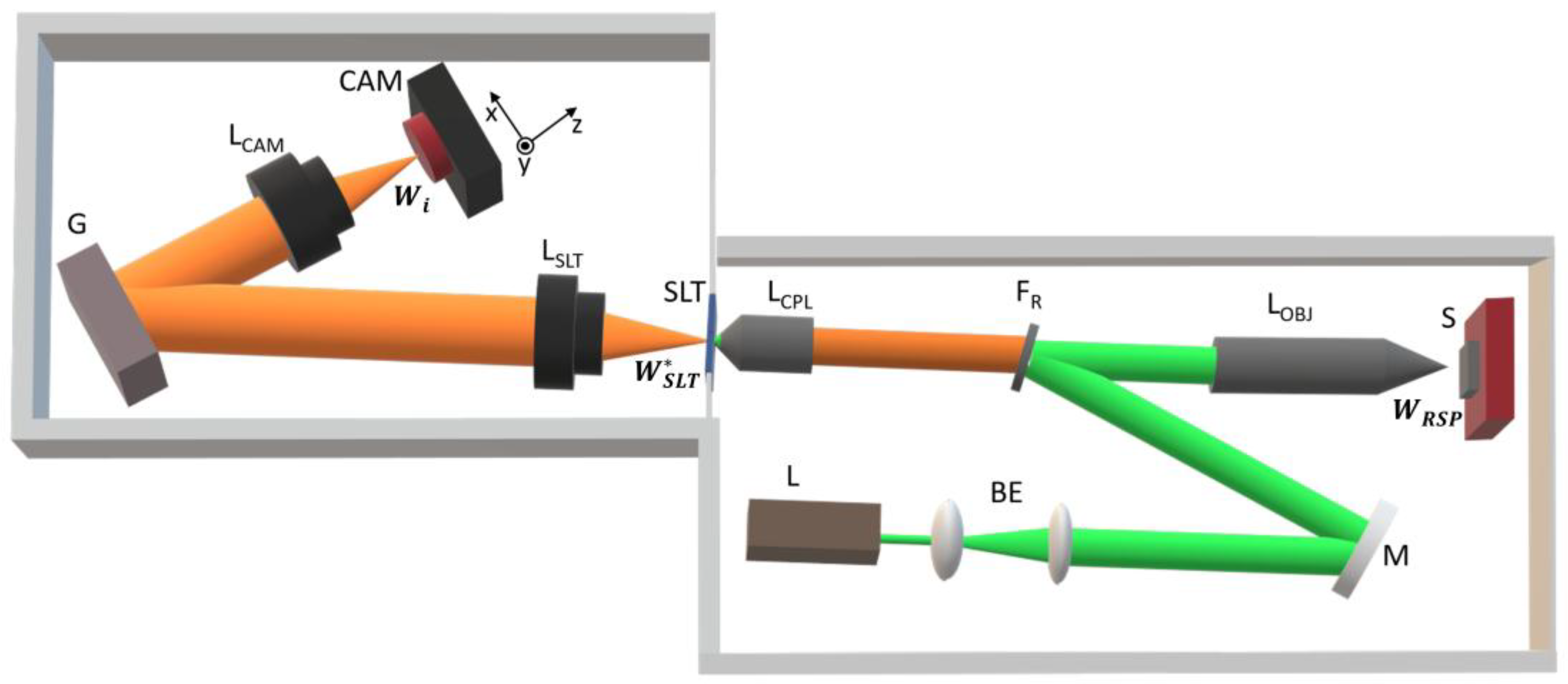
Figure 2.
A. Raman spectrum of calcite crystal measured with µRS with CAM-S (1.85 µm pixel size) as detector using exposure of 3 s and excitation power of 1.6 mW; B. Experimentally evaluated spectral resolution by using three calcite peaks that have been measured with: Renishaw InVia with 100x objective, (black dots), µRS with CAM-L (3.45 µm pixel size, red squares) and µRS with CAM-S (blue dots). The exposure and excitation power was as in A. The spectral resolution function of the µRS (both cameras) is shown as blue line. C. The 1085 cm-1 peak of calcite measured with Renishaw InVia and 100x objective (black curve), with µRS with CAM-L (red curve), and with µRS with CAM-S (blue curve). The peaks are normalized.
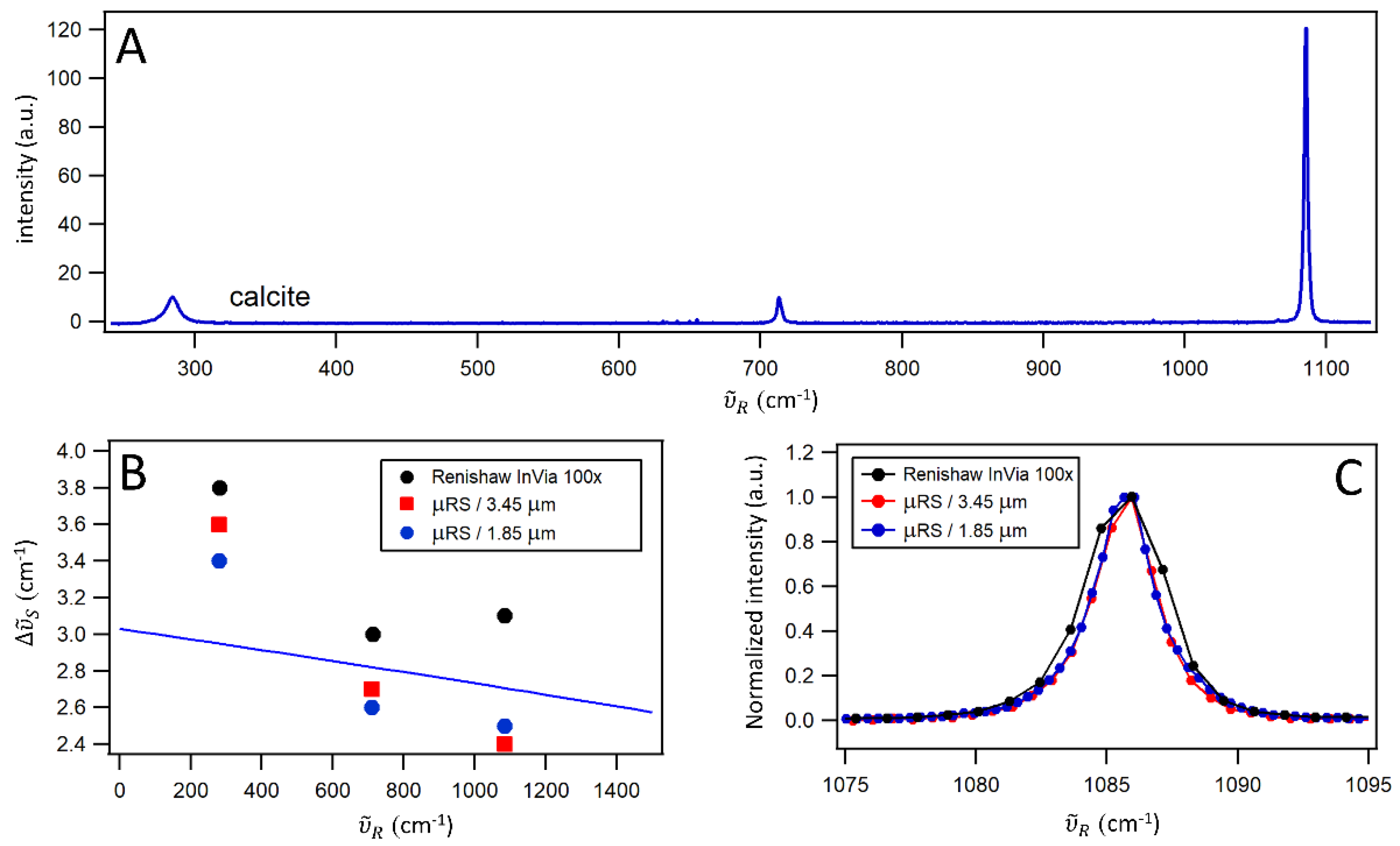
Figure 3.
Monolayer of MoS₂ deposited on the SiO₂/Si substrate used as the SNR calibration sample. Raman spectra of the sample obtained with: A. µRS with CAM-L (1.85 µm pixel size); B. µRS with CAM-S (3.45 µm pixel size); C. Renishaw InVia confocal Raman microscope with a 100× objective. In all experiments, a 1.1 mW excitation at 532 nm was used. The camera exposure times are color-coded, and the two longest exposure spectra have been shifted for clarity. In each panel, for the longest exposure spectra the SNR value was given in parenthesis.
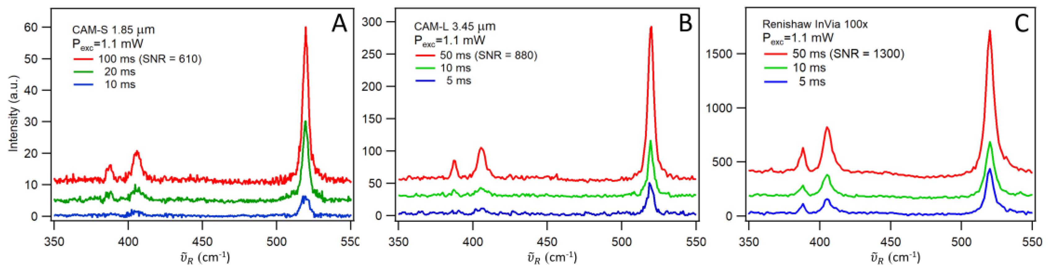
Figure 4.
Comparison of Raman spectra of carbon tetrachloride (CCl₄) measured with Renishaw InVia with a 100× objective and an integration time of 2.5 s (black curve), µRS with CAM-L (3.45 µm pixel size) and an integration time of 2.5 s (red curve), and µRS with CAM-S (1.85 µm pixel size) and an integration time of 10 s (blue curve). Dots indicate the pixel positions. The table presents the following values: ref – central position of the Raman peak from ref. [32]; Δ – difference between the central position of the Raman peak measured with µRS using CAM-S and the reference value.
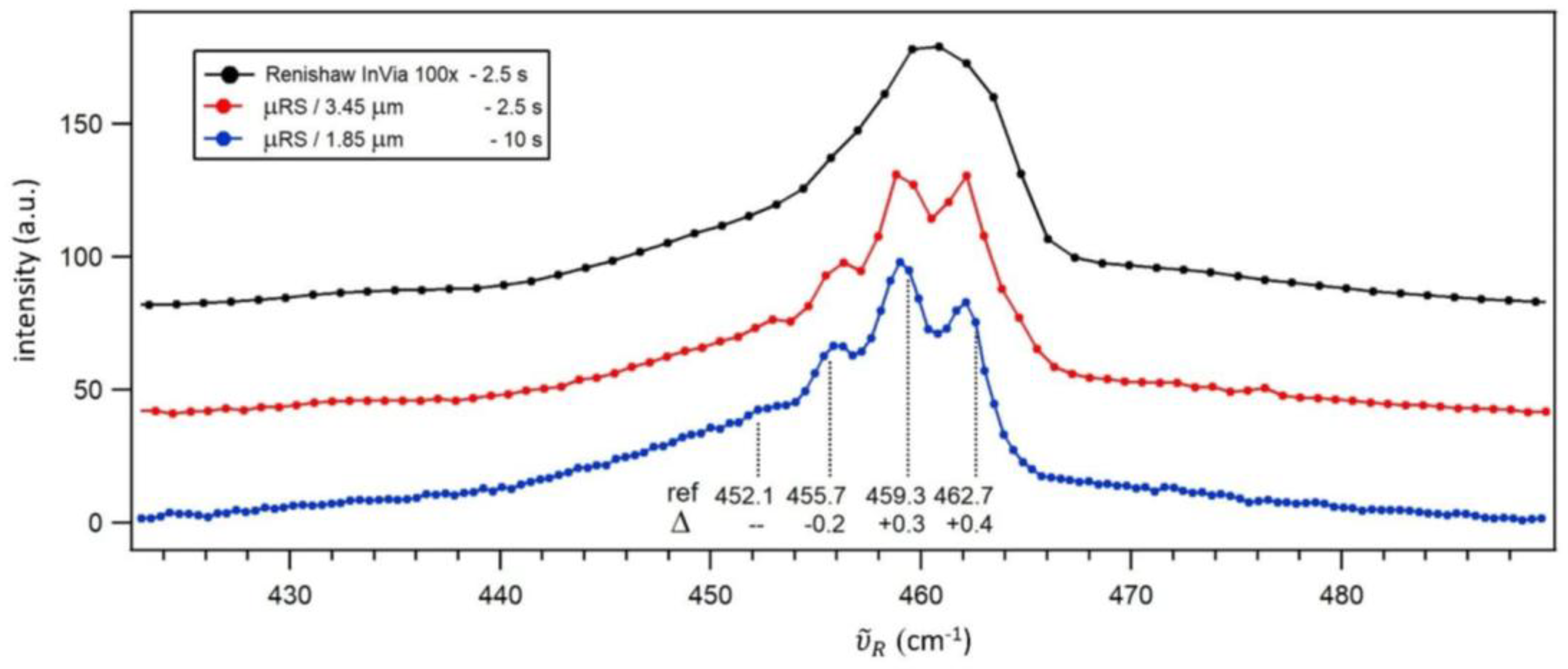

Table 1.
Parameters of the spectrometer and of the calcite Raman peaks from Figure 2: central position of the Raman peak ; natural linewidth; experimental spectral resolution ; the FWHM of the RSP spot image at the detector ; the smallest possible FWHM of the slit image ; wavelength .
Table 1.
Parameters of the spectrometer and of the calcite Raman peaks from Figure 2: central position of the Raman peak ; natural linewidth; experimental spectral resolution ; the FWHM of the RSP spot image at the detector ; the smallest possible FWHM of the slit image ; wavelength .
| detector | [cm-1] | [cm-1] | [cm-1] | [µm] | [µm] | [µm] |
| CAM-L | 280 | 9 | 3.6 | 14.5 | 14.3 | 0.5402 |
| 710 | 2 | 2.7 | 11.6 | 11.4 | 0.5530 | |
| 1085 | 1 | 2.4 | 10.8 | 10.6 | 0.5648 | |
| CAM-S | 280 | 9 | 3.4 | 13.7 | 13.5 | 0.5402 |
| 710 | 2 | 2.6 | 11.2 | 11.0 | 0.5530 | |
| 1085 | 1 | 2.5 | 11.3 | 11.1 | 0.5648 |
Disclaimer/Publisher’s Note: The statements, opinions and data contained in all publications are solely those of the individual author(s) and contributor(s) and not of MDPI and/or the editor(s). MDPI and/or the editor(s) disclaim responsibility for any injury to people or property resulting from any ideas, methods, instructions or products referred to in the content. |
© 2025 by the authors. Licensee MDPI, Basel, Switzerland. This article is an open access article distributed under the terms and conditions of the Creative Commons Attribution (CC BY) license (http://creativecommons.org/licenses/by/4.0/).
Copyright: This open access article is published under a Creative Commons CC BY 4.0 license, which permit the free download, distribution, and reuse, provided that the author and preprint are cited in any reuse.


