Submitted:
10 March 2025
Posted:
11 March 2025
You are already at the latest version
Abstract
The anti-reflective properties of silicon surfaces play a pivotal role in determining the light absorption efficiency of various silicon-based optoelectronic devices, with surface micro-nanostructures emerging as a crucial technological approach for achieving enhanced anti-reflection. In this study, inverted pyramid structures were employed as the micron-scale framework, and micro-nano composite structures were successfully fabricated using an inductively coupled plasma (ICP) etching system. This paper, mainly focused on the micro-nano fabrication, investigated the effects of gas flow rate ratio (SF₆:O₂:C₄F₈), ICP power, RF power, and etching time on the surface morphology and reflectance of the composite structures. The results demonstrate that the optimal anti-reflective micro-nano composite structure was achieved under the following conditions: SF₆ flow rate of 18 sccm, O₂ flow rate of 9 sccm, C₄F₈ flow rate of 4 sccm, ICP power of 300 W, RF power of 5 W, and etching time of 5 minutes. The average reflectivity of the fabricated surface structure was as low as 1.86%.
Keywords:
micro-nano composite structures
; antireflection
; inductively coupled plasma
1. Introduction
Silicon, as a core material in the modern semiconductor industry, is widely used in photovoltaic power generation, optoelectronic devices, biosensors[1,2,3], and other fields. However, due to the high refractive index of silicon, intense Fresnel reflection occurs when light transitions from air into silicon, significantly limiting light absorption efficiency. To address this issue, researchers have proposed various strategies to reduce light reflection and enhance light utilization. Currently, the mainstream technical approaches for reducing reflection are anti-reflection coatings and the fabrication of surface micro-nano structures[4]. Anti-reflection coatings are typically designed based on interference effects at specific wavelengths and incident angles, which limits their working angles. Surface micro/nano structure technology has consistently been a focal point of research and interest. Micro-nano structures reduce light reflection and improve absorption efficiency by expanding the contact area, increasing the number of refractions, and changing the equivalent refractive index. In current research, micron-scale structures such as pyramids, V-grooves, and inverted pyramids[5,6] have been proposed. However, these single micron-scale structures only increase the contact area and the number of refractions between light and the silicon surface, offering limited reduction in reflection. Meanwhile, researchers have also proposed more complex nanostructures such as nano-cones, nano-pillar arrays, and biomimetic moth-eye structures[7,8] to form gradient refractive index layers for reducing reflectivity. However, the intricate nature of these structures poses significant challenges for their fabrication. Combining the two approaches, the integration of simple nanostructures onto micron-scale frameworks to form composite structures has emerged as a more effective solution.
In recent years, researchers have proposed and fabricated various composite structures, typically using a two-step method: first preparing micron-scale structures and then adding nano-scale structures. Chen et al.[9] utilized laser cleaning-assisted laser ablation technology to prepare multi-scale Micro-nano structures in ambient air, demonstrating silicon surfaces with ultralow reflectivity. Yue et al.[10] respectively prepared Micro-nano composite structures on silicon surfaces using reactive ion etching (RIE) technology, achieving excellent anti-reflection performance. Li et al.[11] reported Micro-nano composite structures decorated with gold nanoparticles on silicon surfaces, achieving extremely low reflectivity, but with certain limitations in terms of cost and environmental friendliness. Current research focuses on preparing nano-scale structures on protruding micron-scale structures, resulting in poor mechanical stability of the nano-scale structures. Existing studies have shown that the light-trapping capability of inverted pyramid structures is superior to other structures[12], but there are few reports on combining inverted pyramid structures with nano-scale structures to form composite structures. This paper adopts a two-step method to prepare composite structures, combining inverted pyramid structures with nanostructures to form composite structures with enhanced anti-reflective properties. The effects of gas flow rate ratio (SF₆:O₂:C₄F₈), ICP power, RF power, and time on the formation of nano-scale structures in inductively coupled plasma (ICP) etching technology were investigated.
2. Materials and Methods
2.1. Materials
Monocrystalline silicon wafers (P-type, (100) orientation, resistivity 1-10 Ω·cm, 20 mm × 20 mm, Suzhou Yan Cai Micro-Nano Technology Co. Ltd.); Photoresist (SPR-955, Futurrex); Potassium hydroxide (KOH); Isopropyl alcohol (IPA); Hydrofluoric acid (HF); Deionized water; SF6 (99.999%); O2 (99.999%); C4F8 (99.999%).
2.2. Preparation of Composite Structures
The inverted pyramid structures were prepared using photolithographic patterning-assisted wet etching. The silicon wafers were cleaned using the standard RCA method, followed by thermal oxidation to grow a 150 nm thick SiO2 layer. Periodic square patterns with a size of 10 μm and a spacing of 2 μm were photolithographically defined on the surface. The SiO2 layer within the square patterns was removed by dry etching. The patterned silicon wafers were immersed in a 30% KOH solution doped with 10% IPA and etched in a water bath at 80°C. A magnetic stirrer was used to maintain uniform concentration and temperature of the solution. After etching for 8 minutes and 30 seconds, the wafers were removed, rinsed with deionized water, and immersed in a 5% HF solution for 30 seconds to remove the surface mask and residual oxides. The wafers were rinsed again with deionized water, dried with nitrogen, and stored in a nitrogen cabinet. Nanostructures were prepared using inductively coupled plasma (ICP) etching technology. The silicon wafers with prepared inverted pyramid structures were placed in the sample loading chamber of the ICP etching machine (SENTECH/SI 500, Germany). The chamber was evacuated to match the pressure of the main chamber, and the samples were then transferred for processing. The gas flow rate ratio (SF₆:O₂:C₄F₈), ICP power, RF power, and etching time were adjusted to study the effects of these parameters on the surface morphology and anti-reflection performance of the samples.
The surface morphology of the composite structures was observed using a field emission scanning electron microscope (FEI/Verios 460, Czech Republic). The surface reflectance of different samples was measured using a spectrophotometer (Shimadzu/UV3600, Japan, equipped with an integrating sphere) in the wavelength range of 300-800 nm.
3. Results and Discussion
The ICP system primarily relies on high-frequency power to excite inert gas, generating high-density plasma that decomposes reactive gases (SF₆:O₂:C₄F₈) into active radicals and ions. SF6 decomposition provides fluorine radicals (F) to etch silicon, O2 decomposes into oxygen atoms (O) that react with silicon (Si) to form a passivation layer, and C4F8 decomposes to generate fluorocarbon polymers (CFₓ), forming a sidewall protection layer to enhance anisotropy[13]. The chemical reactions are as follows:
The gaseous byproducts generated during the etching reaction are evacuated by the vacuum pump of the ICP system, ensuring the continuous progress of the reaction.
Figure 1a is the SEM image of the prepared inverted pyramid structure, indicating that the inverted pyramid structures on the silicon surface are uniformly arranged, structurally intact, and highly reproducible. Figure 1b is the SEM image of the 45° inclined surface of the inverted pyramid structure, revealing a smooth internal surface without residues, confirming the successful preparation of the structure. Figure 1c displays the reflectivity of planar silicon and inverted pyramid-structured silicon, the reflectance of the inverted pyramid-structured silicon is significantly lower than that of planar silicon, with a notable improvement in anti-reflection performance. The average reflectance decreased from 39.80% to 13.85%, a reduction of 68.72%. The inverted pyramid-structured substrate demonstrates excellent anti-reflection properties, providing a foundation for subsequent nanostructure preparation and further reduction of reflectance.
The flow rate ratio of SF6 to O2 is a critical factor in the etching process. By controlling the etching time to 5 minutes, ICP power to 300 W, and RF power to 0 W, the formation of nanostructures under different flow rate ratios was investigated. Figure 2 is the SEM images of surfaces etched with different SF6:O2 flow rate ratios. From Figure 2a,b, it can be observed that at lower O2 ratios, the inverted pyramid structures are damaged, and no significant nanostructures are formed. The sidewall profiles tend to become rounded. This is because the passivation effect of O2 at low ratios cannot compete with the etching effect of SF6. Higher SF6 concentrations result in faster etching rates, but insufficient O2 content leads to inadequate formation of an oxide mask, resulting in poor anisotropy. As the O2 content increases, the etching results are shown in Figure 2c,d. The inverted pyramid profiles remain intact, and the sidewall angles are preserved, but no significant nanostructures are formed, with only small protrusions on the sidewall surfaces. Further increasing the O2 ratio, as shown in Figure 2e,f, shows oxide deposition at grain boundaries and the bottom due to the accelerated formation of the oxide mask caused by the higher O2 concentration, which inhibits the etching rate. Throughout the etching process, fluorine ions from SF6 provide chemical etching capability, while O2 generates an oxide mask protective layer[14]. However, at room temperature, no effective nanostructures are formed under all condition cases. C4F8 was introduced in subsequent experiments to balance passivation and etching effects. C4F8 generates fluorocarbon films that deposit on the sidewalls of nanostructures, effectively suppressing lateral etching and protecting the nanostructures from damage.
With SF6 fixed at 18 sccm, O2 at 9 sccm, ICP power at 300 W, RF power at 0 W, and etching time at 5 minutes, Figure 3a–c show the SEM images of composite structures under C4F8 flow rates of 0 sccm, 4 sccm, and 8 sccm, respectively. Figure 3a depicts the etching morphology without the introduction of C4F8, where no effective nanostructures are formed, and the bottom of the inverted pyramid structures is damaged, with oxide deposition observed at grain boundaries and the bottom. Figure 3b shows the etching morphology with the addition of 4 sccm C4F8, where hollow-like nanostructures are formed. Figure 3c presents the etching morphology with 8 sccm C4F8, where the nanostructures at the bottom disappear, and the nanostructures on the sidewalls of the inverted pyramid structures remain incompletely formed. This is because the introduction of C4F8 generates fluorocarbon films that deposit on the sidewalls of the nanostructures, enhancing anisotropic etching. However, excessive C4F8 leads to the over-formation of fluorocarbon compounds, resulting in residues that inhibit etching. Figure 3d compares the reflectivity spectra of composite-structured silicon wafers under different C4F8 flow rates. The average reflectance values are 16.3%, 5.56%, and 8.71% for C4F8 flow rates of 0 sccm, 4 sccm, and 8 sccm, respectively. Without the addition of C4F8, the average reflectance increases by 2.45% due to the lack of effective nanostructures, which causes the inverted pyramid structures to be etched and their depth reduced, thereby diminishing their anti-reflection capability.
ICP power directly affects the plasma density. With SF6 fixed at 18 sccm, O2 at 9 sccm, C4F8 at 4 sccm, RF power at 0 W, and etching time at 5 minutes, Figure 4a shows the SEM image at an ICP power of 150 W, where small hill-like protrusions are formed on the sidewalls of the inverted pyramid structures, but the nanostructures are sparse due to low plasma density and insufficient etching reactions. When the power is increased to 300 W, as shown in Figure 4b, a dynamic balance between etching and passivation ion densities in the plasma is achieved, resulting in the formation of hollow-like nanostructures on the surface, which effectively reduce reflectance. Further increasing the power to 450 W, as shown in Figure 4c, reveals polymer deposition at the grain boundaries of the structures due to the excessive heat generated at high power[15], which damages the nanostructures. Figure 4d compares the reflectivity spectra of composite structures under different ICP powers. The average reflectance values are 9.49%, 5.56%, and 8.15% for ICP powers of 150 W, 300 W, and 450 W, respectively. This is because the combination of nanostructures and microstructures creates a gradual refractive index transition from air to the silicon substrate, effectively reducing reflectance. This effect is particularly pronounced in the 300 to 550 nm wavelength range, as shorter wavelengths are more sensitive to changes in refractive index.
The radio frequency (RF) power primarily affects the energy of ions and the directionality of etching during the formation of nanostructures. With SF6 fixed at 18 sccm, O2 at 9 sccm, C4F8 at 4 sccm, ICP power at 300 W, and etching time at 5 minutes. Figure 5a–c show the SEM images of composite structure surfaces under different RF powers, revealing that nanostructures are still formed as the RF power increases. Figure 5b shows the SEM image of the composite structure surface morphology at an RF power of 5 W. Compared to the sample without RF power, circular pore-like nanostructures are formed, and the overall morphology of the composite structure is more complete, with more regular nanostructures. This is because the application of RF power provides directional energy to the radical ions, resulting in better anisotropy. Figure 5c shows the SEM image of the composite structure surface morphology at an RF power of 10 W. As the RF power further increases, the radical ions acquire more energy, resulting in the degradation of nanostructures. However, the depth of the inverted pyramid structure increases, which also contributes to anti-reflection. Figure 5d compares the reflectivity spectra of composite-structured silicon wafers at RF powers of 0 W, 5 W, and 10 W, with average reflectance values of 5.56%, 1.86%, and 3.55%, respectively. When the RF power is set to 5 W, the reflectivity is reduced to merely 1.86%, representing a 37.94% decrease compared to planar silicon wafers.
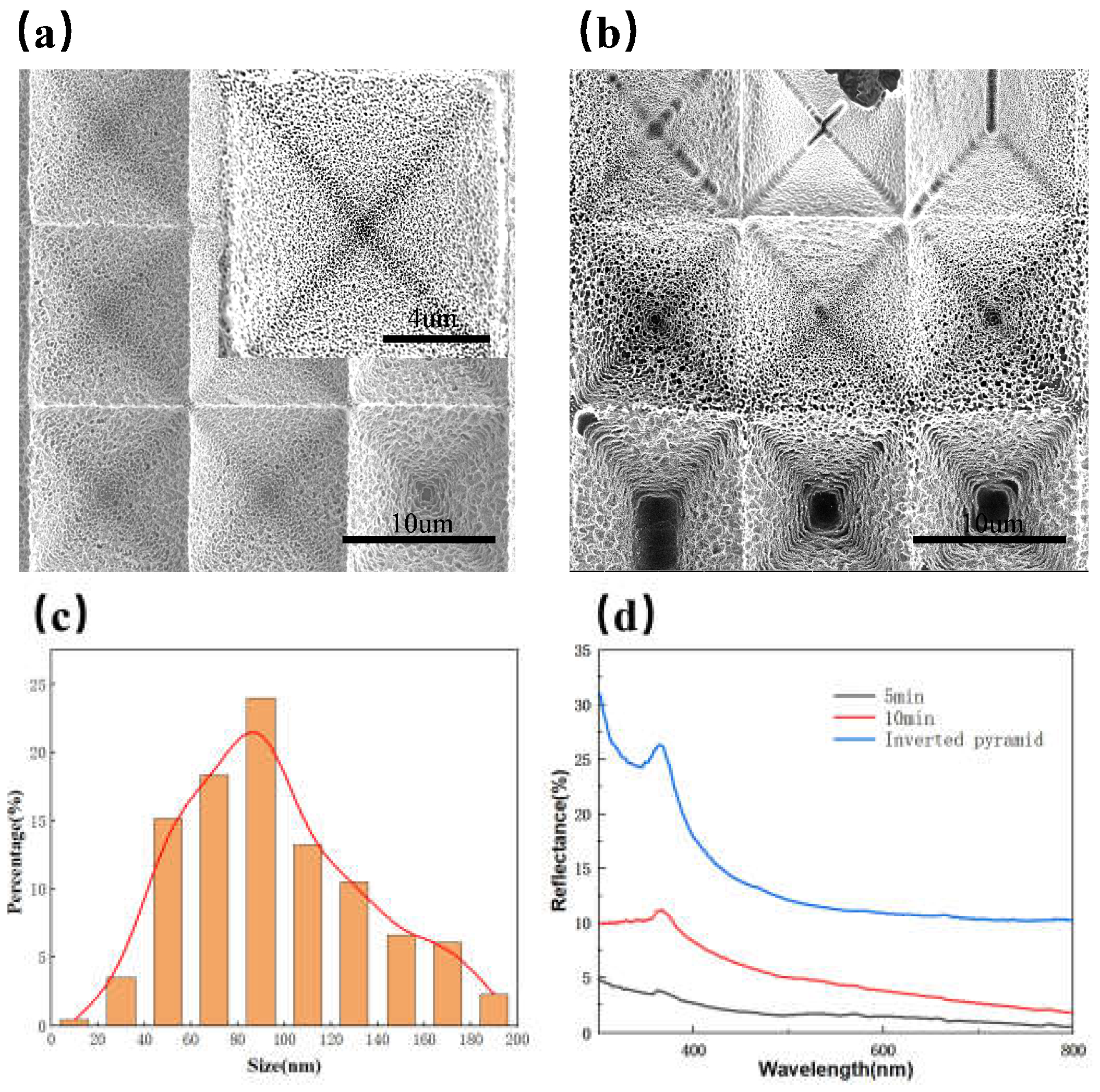
Figure 6a,b shows the surface morphology of composite structures under different etching times. It is evident that as the etching time extends to 10 minutes, the inverted pyramid structures undergo damage, and the pores within the nanostructures progressively expand, with some being compromised by lateral etching, ultimately resulting in diminished anti-reflection performance. From the reflectivity spectra in Figure 6d, it is evident that the reflectance significantly increases at an etching time of 10 minutes, with an average value of 5.24%. Figure 6c shows the diameter distribution of the circular pore-like nanostructures formed at 5 minutes of etching. The diameters of the nanostructures are mainly concentrated between 40-140 nm, which effectively reduces the reflectance.
4. Conclusions
Using ICP etching technology, nanostructures were fabricated on silicon wafers with periodic inverted pyramid structures of 10 μm in size and 2 μm in spacing to form composite structures. Research indicates that at room temperature, effective nanostructures cannot be generated using only SF6 and O2 as etching gases, and an appropriate amount of C4F8 is required to balance the reaction. The optimal anti-reflection composite structure was achieved under the conditions of SF6 flow rate at 18 sccm, O2 at 9 sccm, C4F8 at 4 sccm, ICP power at 300 W, RF power at 5 W, and etching time of 5 minutes. This structure exhibited an extremely low reflectance of 1.86% in the wavelength range of 300-800 nm, representing a reduction in average reflectance by 37.94% compared to planar silicon wafers.
Author Contributions
Conceptualization, investigation, methodology, formal analysis, data curation, and writing—review and editing, Z.F.; investigation, and formal analysis L.X.; formal analysis, B.Z.; supervision, project administration, funding acquisition, and writing—review and editing, T.C. All authors have read and agreed to the published version of the manuscript.
Funding
This research was funded by the Beijing Natural Science Foundation-Huairou Innovation Joint Fund Project (project No. L245012).
Data Availability Statement
Not applicable.
Acknowledgments
This work was supported by the Laser Engineering Research Institute of Beijing University of Technology and the Beijing Natural Science Foundation-Huairou Innovation Joint Fund (Project No. L245012).
Conflicts of Interest
The authors declare that they have no known competing financial interests or personal relationships that could have appeared to influence the work reported in this paper.
References
- Pera D M, Costa I, Serra F, et al. Development of a metal-assisted chemical etching method to improve light-capture in monocrystalline silicon solar cells[J]. Solar Energy Materials and Solar Cells, 2023, 251: 112143. [CrossRef]
- Serpengüzel A, Kurt A, Inanç I, et al. Luminescence of black silicon[J]. Journal of Nanophotonics, 2008, 2(1): 021770. [CrossRef]
- Fang H, Yu K J, Gloschat C, et al. Capacitively coupled arrays of multiplexed flexible silicon transistors for long-term cardiac electrophysiology[J]. Nature biomedical engineering, 2017, 1(3): 0038. [CrossRef]
- Yeo R J, Wu W Y, Tomczak N, et al. Tailoring surface reflectance through nanostructured materials design for energy-efficient applications[J]. Materials Today Chemistry, 2023, 30: 101593.
- Almenabawy S, Zhang Y, Flood A, et al. Nanometer-mesa inverted-pyramid photonic crystals for thin silicon solar cells[J]. ACS Applied Energy Materials, 2022, 5(11): 13808-13816. [CrossRef]
- Feng B, Chen W, **ng G, et al. Influence of inverted pyramid texturization on front metallization and performance of crystalline silicon solar cells[J]. Solar Energy Materials and Solar Cells, 2024, 272: 112919. [CrossRef]
- Rahman T, Navarro-Cía M, Fobelets K. High density micro-pyramids with silicon nanowire array for photovoltaic applications[J]. Nanotechnology, 2014, 25(48): 485202. [CrossRef]
- Lan J, Yang Y, Hu S. Numerical Study on Broadband Antireflection of Moth-Eye Nanostructured Polymer Film with Flexible Polyethylene Terephthalate Substrate[J]. Nanomaterials, 2021, 11(12): 3313. [CrossRef]
- Sainiemi L, Jokinen V, Shah A, et al. Non-reflecting silicon and polymer surfaces by plasma etching and replication[J]. Advanced materials, 2011, 23(1): 122-126. [CrossRef]
- Yue Z, Shen H, Jiang Y. Antireflective nanostructures fabricated by reactive ion etching method on pyramid-structured silicon surface[J]. Applied Surface Science, 2013, 271: 402-406. [CrossRef]
- Yao C, Liu Y, Niu J, et al. Micro/nano-hybrid hierarchical structure of black silicon decorated with gold nanoparticles for ultralow broadband reflectivity (< 1%)[J]. Applied Surface Science, 2024, 655: 159641. [CrossRef]
- Sun Z, Chen W, Zhang X, et al. Chain pyramid texturization for better light trap and efficiency of silicon solar cells[J]. Solar Energy Materials and Solar Cells, 2023, 251: 112137. [CrossRef]
- Susarrey-Arce A, Marin A G, Nair H, et al. Absence of an evaporation-driven wetting transition on omniphobic surfaces[J]. Soft Matter, 2012, 8(38): 9765-9770. [CrossRef]
- Sainiemi L, Jokinen V, Shah A, et al. Non-reflecting silicon and polymer surfaces by plasma etching and replication[J]. Advanced materials, 2011, 23(1): 122-126. [CrossRef]
- Tinck S, Tillocher T, Georgieva V, et al. Concurrent effects of wafer temperature and oxygen fraction on cryogenic silicon etching with SF6/O2 plasmas[J]. Plasma Processes and Polymers, 2017, 14(9): 1700018.
Figure 1.
(a) SEM image of the inverted pyramid structure. (b) SEM image of the 45° inclined surface of the inverted pyramid structure. (c) Reflectivity spectra of planar silicon and inverted pyramid-structured silicon.
Figure 1.
(a) SEM image of the inverted pyramid structure. (b) SEM image of the 45° inclined surface of the inverted pyramid structure. (c) Reflectivity spectra of planar silicon and inverted pyramid-structured silicon.
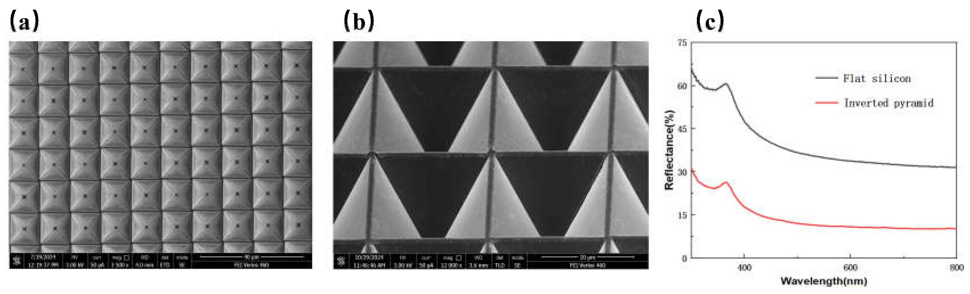
Figure 2.
SEM images of surfaces etched with different SF6:O2 rate ratios. SF6:O2 (sccm): (a) 18:3; (b) 18:6; (c) 18:9; (d) 18:12; (e) 18:15; (f) 18:18.
Figure 2.
SEM images of surfaces etched with different SF6:O2 rate ratios. SF6:O2 (sccm): (a) 18:3; (b) 18:6; (c) 18:9; (d) 18:12; (e) 18:15; (f) 18:18.
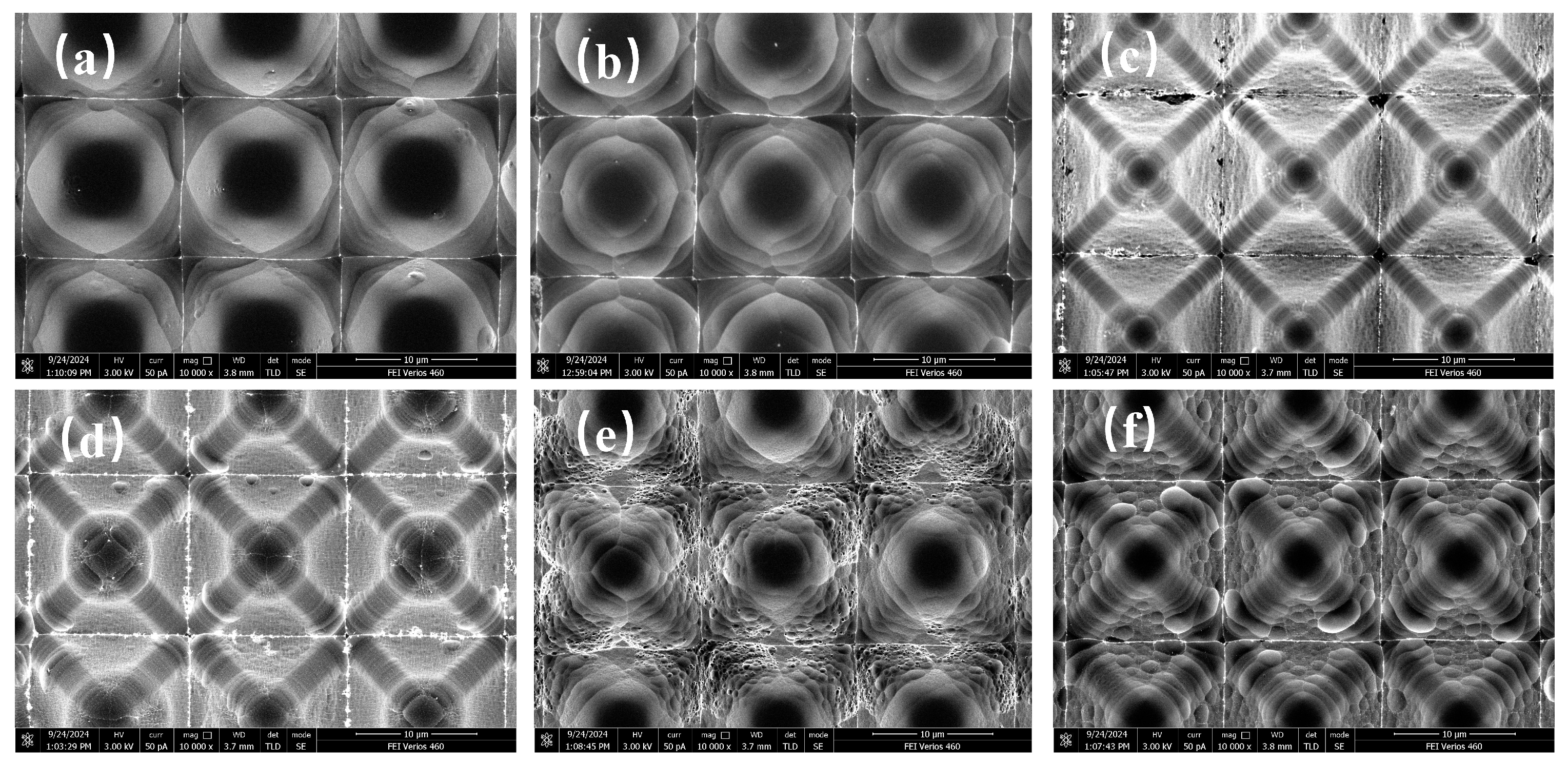
Figure 3.
SEM images of composite structures under different C4F8 flow rates. (a) 0 sccm; (b) 4 sccm; (c) 8 sccm; (d) Reflectivity spectra of composite-structured silicon wafers under different C4F8 flow rates.
Figure 3.
SEM images of composite structures under different C4F8 flow rates. (a) 0 sccm; (b) 4 sccm; (c) 8 sccm; (d) Reflectivity spectra of composite-structured silicon wafers under different C4F8 flow rates.
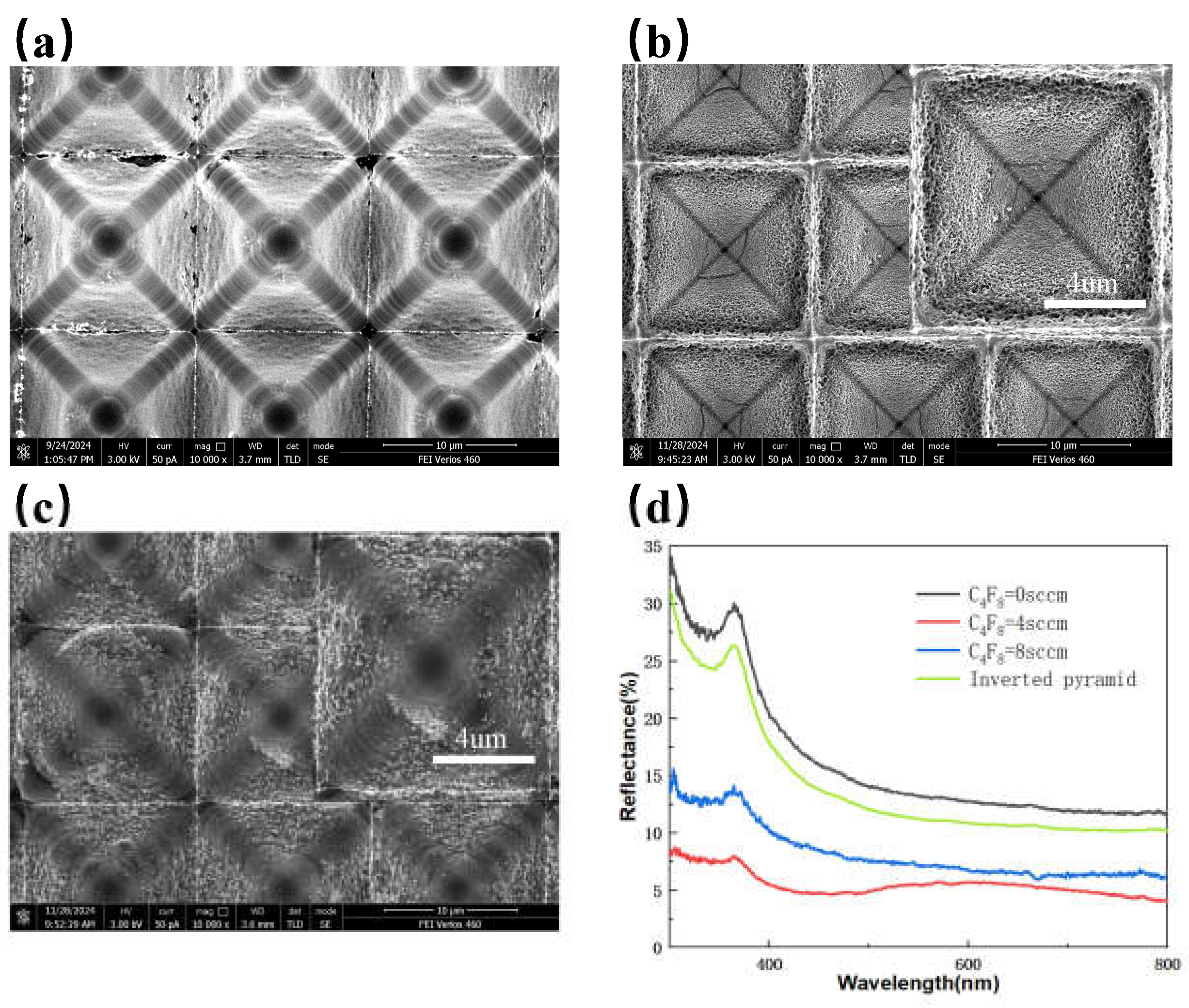
Figure 4.
SEM images of composite structures under different ICP powers: (a) 150 W; (b) 300 W; (c) 450 W; (d) Reflectivity spectra of composite-structured silicon wafers under different ICP powers.
Figure 4.
SEM images of composite structures under different ICP powers: (a) 150 W; (b) 300 W; (c) 450 W; (d) Reflectivity spectra of composite-structured silicon wafers under different ICP powers.
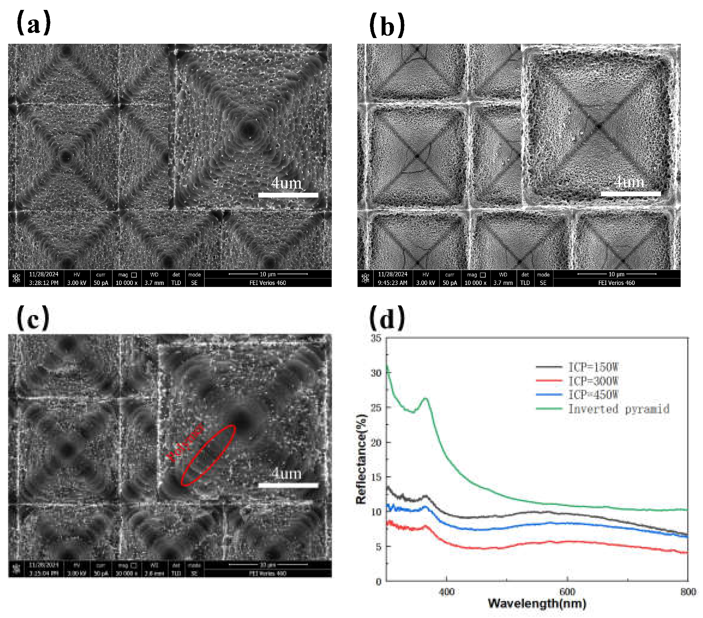
Figure 5.
SEM images of composite structures under different RF powers. (a) 0 W; (b) 5 W; (c) 10 W; (d) Reflectivity spectra of composite-structured silicon wafers under different RF powers.
Figure 5.
SEM images of composite structures under different RF powers. (a) 0 W; (b) 5 W; (c) 10 W; (d) Reflectivity spectra of composite-structured silicon wafers under different RF powers.
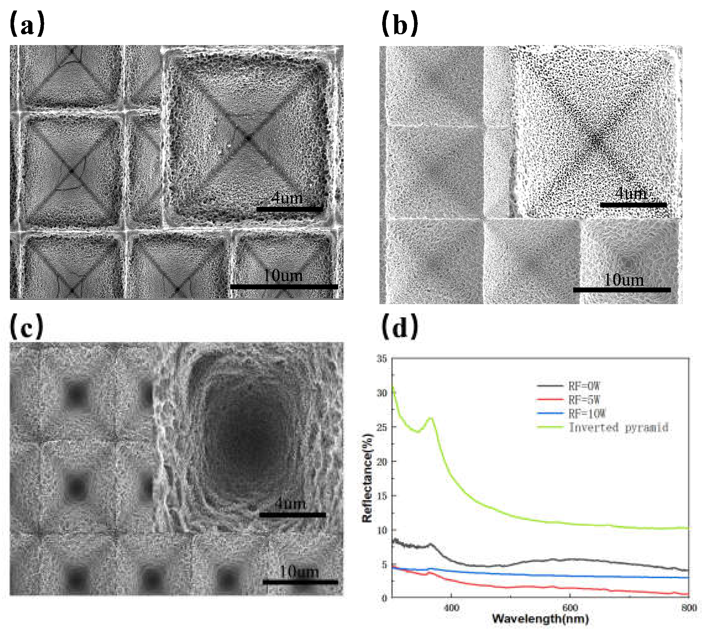
Figure 6.
SEM images of composite structures under different etching times. (a) 5 minutes; (b) 10 minutes; (c) Pore size distribution of nanostructures at 5 minutes; (d) Reflectivity spectra of composite-structured silicon wafers at different times.
Figure 6.
SEM images of composite structures under different etching times. (a) 5 minutes; (b) 10 minutes; (c) Pore size distribution of nanostructures at 5 minutes; (d) Reflectivity spectra of composite-structured silicon wafers at different times.
Disclaimer/Publisher’s Note: The statements, opinions and data contained in all publications are solely those of the individual author(s) and contributor(s) and not of MDPI and/or the editor(s). MDPI and/or the editor(s) disclaim responsibility for any injury to people or property resulting from any ideas, methods, instructions or products referred to in the content. |
© 2025 by the authors. Licensee MDPI, Basel, Switzerland. This article is an open access article distributed under the terms and conditions of the Creative Commons Attribution (CC BY) license (http://creativecommons.org/licenses/by/4.0/).
Copyright: This open access article is published under a Creative Commons CC BY 4.0 license, which permit the free download, distribution, and reuse, provided that the author and preprint are cited in any reuse.


