Preprint
Article

This version is not peer-reviewed.

Simulation Analysis of Magnetic - Sensitive Sensors under Transient Strong Electromagnetic Interference and High Temperature and Optimization of Packaging Structures

Submitted:

04 March 2025

Posted:

05 March 2025

You are already at the latest version

Abstract

In smart grids, magnetic-sensitive sensors encounter reliability issues due to transient electromagnetic interference (EMI) and elevated temperatures. This study employs the finite-element method, focusing on current-testing sensors used in gas-insulated substations. By utilizing a damping oscillation wave as the excitation source, a simulation analysis compares the epoxy-molding compound's performance both with and without a copper shielding layer. Findings reveal that, in the absence of a shielding layer, the electric field, magnetic field, and current density responses at the detection points of the chip and bonding wires exhibit damping oscillations correlating with the excitation source. However, introducing the copper shielding layer substantially diminishes these metrics, suggesting its effective role in obstructing interference. Furthermore, a temporal correlation exists between the sensor's electromagnetic field and current density and the excitation source's waveform. When simulating in a high-temperature environment, the sensor's internal stress distribution becomes notably uneven, with pronounced stress concentrations at the gold wire-chip bonding points and solder joints. Notably, deformation is primarily observed in the center of the epoxy-molding compound and at the bonding wires. To mitigate these challenges, a novel packaging structure is introduced. Its shielding body, crafted from 3D-printed resin and filled with electromagnetic shielding materials, offers both electromagnetic shielding and a reduction in thermal expansion-induced stress and strain. Concurrently, a multi-layered shielding design is suggested to amplify the shielding efficacy, serving as a benchmark for sensor optimization.

Keywords: 
;  ;  ;  ;  ;  

1. Introduction

In contemporary power systems, the utilization of magnetic sensors has become increasingly vital. However, electromagnetic interference, especially transient strong electromagnetic interference, significantly affects these systems, leading to measurement inaccuracies and potential system failures [1]. The evolution of smart power systems has heightened the performance expectations for sensors. Yet, transient strong electromagnetic interference, as seen with high-voltage equipment switching operations or lightning strikes, jeopardizes the stability and safety of power systems, underscoring the growing importance of this research area [2-7]. Extensive studies have detailed the impact of electromagnetic interference on electronic devices. It is found that such interference can diminish sensitivity and linearity, amplify measurement errors, and introduce output response distortion at specific frequencies, resulting in equipment failure and system malfunctions. Notably, the sensor’s structure influences its vulnerability to interference [8-13]. Moreover, localized high temperatures frequently arise in power system settings, primarily due to three factors: heat produced by equipment operation, constrained heat dissipation conditions, and abnormal heating from faults. Short-circuit failures triggered by transient strong electromagnetic impacts also contribute to these localized high temperatures. Despite these challenges, limited research has been reported on the impact of transient strong electromagnetic interference and localized high temperatures on the performance of magnetic sensors in substations. Field testing in power system environments with multiple physical fields presents several shortcomings. For instance, complex electromagnetic environments and severe climatic conditions can disrupt testing equipment and outcomes. Additionally, testing equipment often grapples with issues like limited accuracy and sensitivity, and constraints on size and weight.

2. Materials and Methods

2.1. Simulation Analysis of Transient Strong Electromagnetic Field

Transient strong electromagnetic interference (EMI) in power systems originates from power equipment operations, faults, or natural phenomena like lightning strikes. It presents as swiftly fluctuating electric and magnetic fields, enduring from nanoseconds to microseconds. Its amplitude, frequency, and duration variations can affect signal transmission and equipment functionality. Notably, disturbances from equipment operations, such as the creation of Very Fast Transient Overvoltages (VFTO) during the switching of Gas-Insulated Substations (GIS), symbolize a prevalent form of intense electromagnetic interference in power systems. These are typically characterized by damped oscillatory waveforms.
This study utilizes the finite element analysis method, grounded in Maxwell’s equations, to develop a magnetic sensor model that accounts for transient strong electromagnetic interference. The model, depicted in Figure 1, comprises a chip, bonding wires, a molding compound, lead frames, and a solder layer. The chip is represented as silicon, the bonding wire material is gold, the molding compound is epoxy resin, and the lead frame is aluminum. Material parameters for each component are detailed in Table 1. The simulation space is defined by extending the model dimensions by one size along the XYZ axes, with the simulation area designated as air and its boundaries as radiation boundary conditions. A damped oscillatory waveform is used as the excitation source on one boundary surface of the simulation area, simulating the typical electromagnetic interference created by radiative electromagnetic coupling between secondary equipment during power system switching operations. The electromagnetic field distribution in the near field and within the components, along with the induced voltage and current, are examined and analyzed. Furthermore, a copper shielding layer is incorporated outside the sensor’s molding compound for a comparative experimental group, to assess the impact of the excitation interference source on the sensor under varied simulation conditions. Detection points 1, 2, 3, and 4 are established at different locations on the bonding wire. Figure 2 illustrates the measured electric field interference values at a 500 kV substation, showing a damped oscillatory wave with a peak amplitude of 16.6 kV occurring at 1.86 μs. The amplitude gradually diminishes over time until it stabilizes, with the waveform persisting for 10.5 μs.

2.2. Thermal-Stress-Strain Physical Field Simulation Analysis

Similarly, the magnetic sensor is selected as the simulation research object, and its structure is shown in Figure 1. The thermodynamic parameters of each component are listed in Table 2.
The study assumes that the sensor is situated in a local high-temperature environment, with an ambient temperature reaching up to 70°C. The heat transfer coefficient is set accordingly to simulate normal air convection for heat transfer. This simulation calculates both the thermal expansion stress and deformation of the sensor under these temperature conditions. The results derived from the thermal analysis are then incorporated into the structural analysis module. Subsequently, the thermal expansion stress and deformation are computed, taking into account material properties and geometric constraints.

3. Results

3.1. Simulation Results of Transient Strong Electromagnetic Field

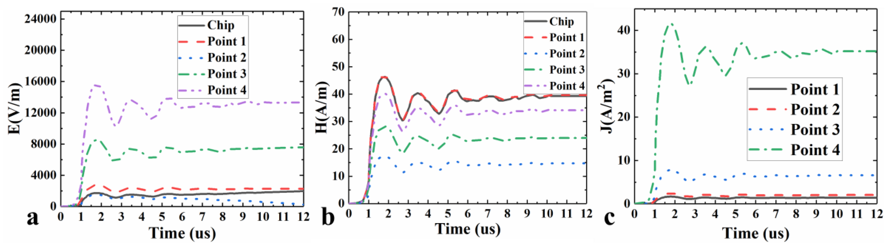
Figure 3 presents the temporal variation of electromagnetic field and current density response values at different detection points on the chip and bonding wires within the sensor, without the incorporation of shielding material. As illustrated in 
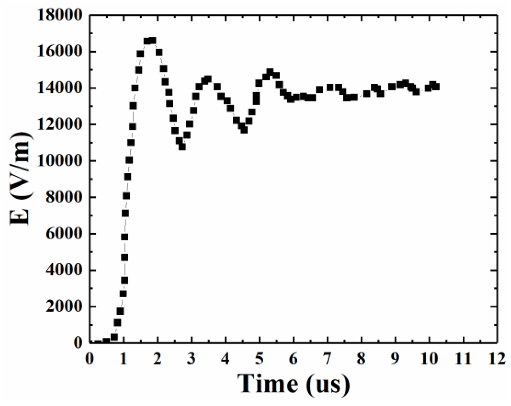
Figure 3a, the waveforms at each detection point generally align with those of the excitation source, indicating a swift response correlation between the electric field strength and the excitation source. A detailed analysis reveals that the peak electric field response amplitude at the chip is observed at 1.85 μs, with respective maximum amplitudes of 2744.89 V/m, 1501.99 V/m, 8505.82 V/m, and 15596.64 V/m. Notably, the electric field response amplitudes at the chip and detection points 1 and 2 on the gold wires are significantly lower, whereas those at detection points 3 and 4 on the bonding wires exhibit larger values. This can be attributed to the proximity of detection points 3 and 4 to the metal lead frames, resulting in elevated electric field response amplitudes.
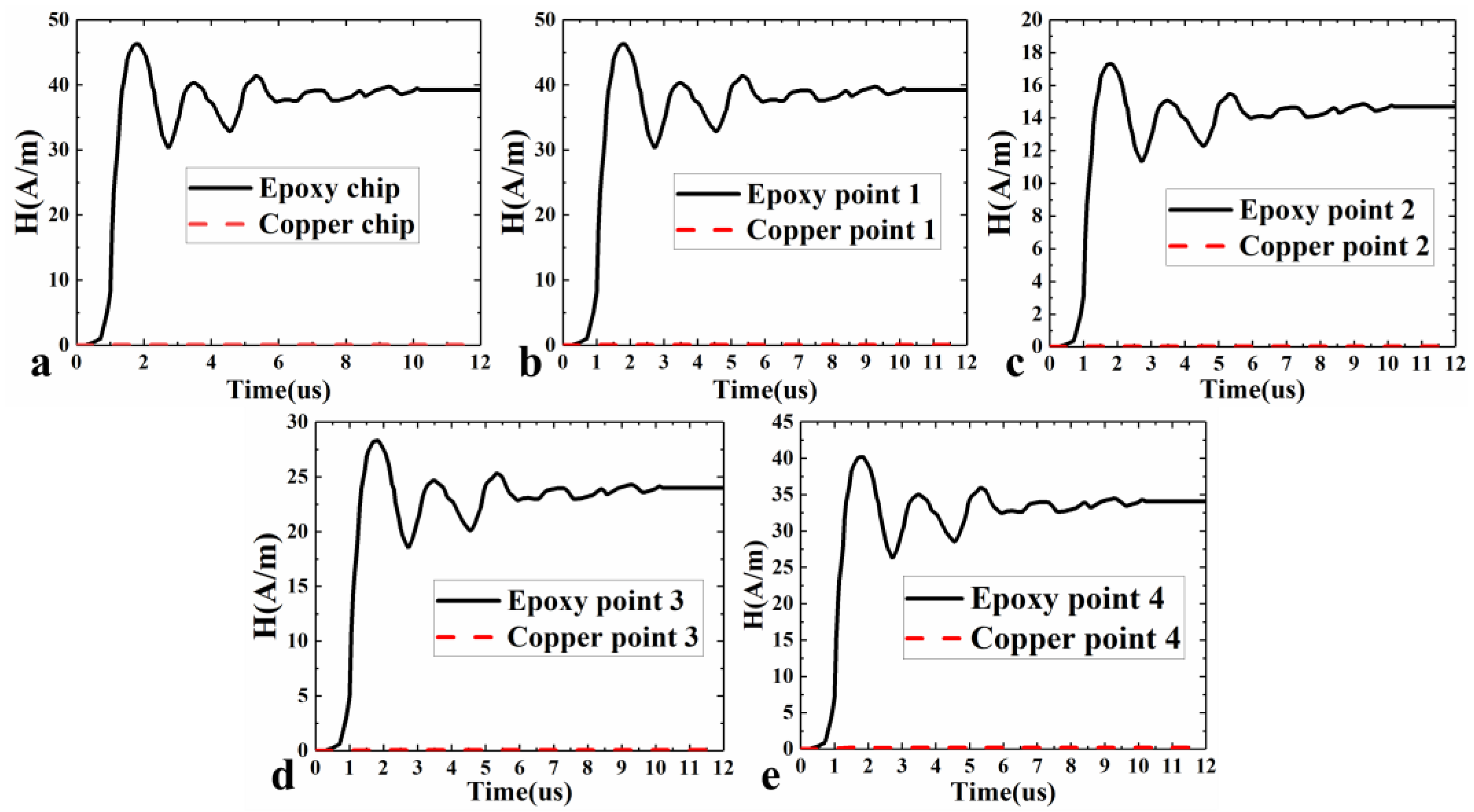
Figure 3b illustrates the temporal variation of magnetic field response values at various detection points on the chip and bonding wires, again without the addition of shielding material. The depicted magnetic field response mirrors the waveform of the excitation source, characterized by a damped oscillatory wave wherein the energy progressively diminishes after attaining the maximum amplitude. The peak magnetic field response intensities at each point are reached at 1.85 μs, with respective values of 46.27 A/m, 46.72 A/m, 17.31 A/m, 28.29 A/m, and 40.18 A/m. In comparison to the electric field response amplitudes, the highest magnetic field response amplitudes are observed at the chip and detection point 1.Finally, 
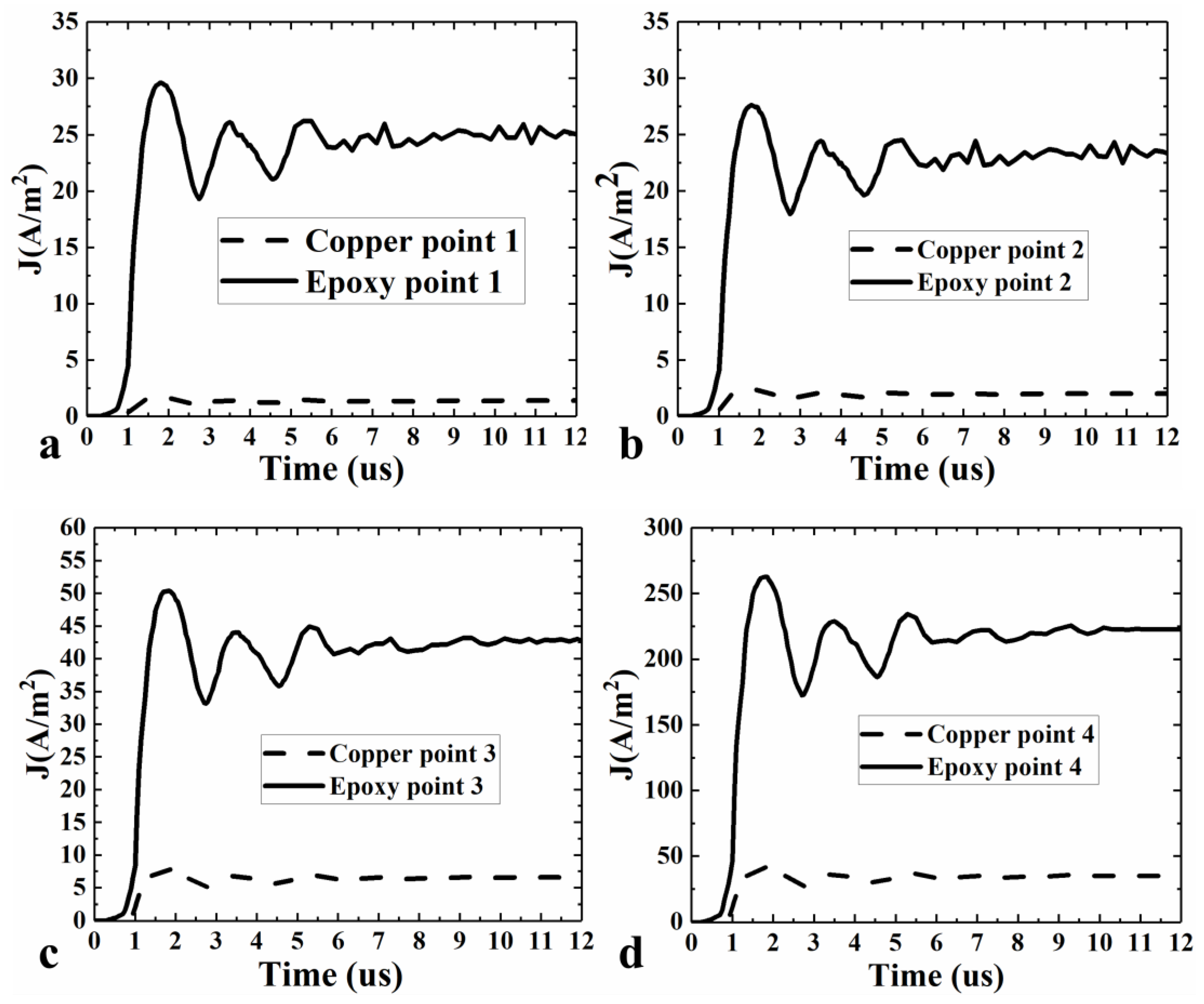
Figure 3c delineates the temporal variation of current density response values at different detection points on the chip and bonding wires, without the integration of shielding material. The current density response adheres to a pattern analogous to that of the excitation source, demonstrating a damped oscillatory wave wherein the energy gradually decays following the attainment of the maximum amplitude.
In a comparative experiment, a copper layer was introduced to the exterior of the molding compound as a shielding layer. The copper material exhibited a conductivity of 5.96×10⁷ S/m, a permeability of 0.999991, and a relative permittivity of 1. The influence of this copper shielding layer on the sensor was assessed both pre- and post-addition. 
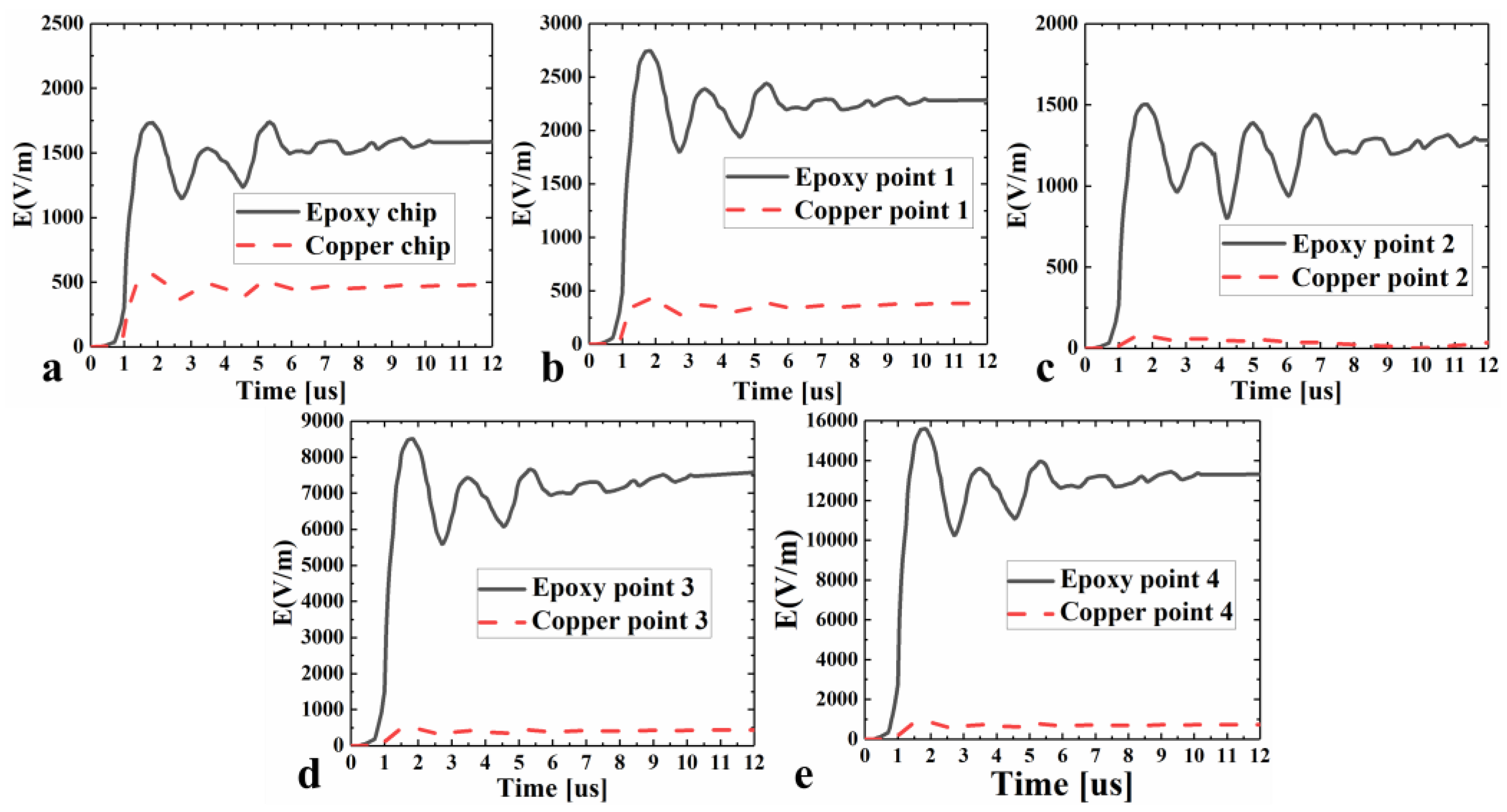
Figure 4 illustrates the temporal variation in electric field strength at different detection points on the chip and bonding wires within the sensor, both with and without the external copper shielding layer. Post-addition of the copper shielding layer, there was a marked reduction in electric field strength at each detection point. Specifically, the peak electric field strength decreased from 1732.87 V/m to 559.68 V/m at the chip detection point, from 2744.89 V/m to 422.43 V/m at bonding wire detection point 1, from 1501.98 V/m to 73.19 V/m at bonding wire detection point 2, from 8505.83 V/m to 480.74 V/m at bonding wire detection point 3, and from 15603.18 V/m to 855.88 V/m at bonding wire detection point 4. Notably, the waveform consistently displayed as a damped oscillatory wave.
Figure 5 depicts the temporal variation of magnetic field strength at different detection points on the chip and bonding wires within the sensor, both pre- and post-application of an external copper shielding layer. The introduction of the copper shielding layer led to a significant reduction in the magnetic field strength at each detection point. Specifically, the peak magnetic field strength decreased from 46.27 A/m to 0.0284 A/m at the chip detection point, from 46.35 A/m to 0.05 A/m at bonding wire detection point 1, from 17.3 A/m to 0.04 A/m at bonding wire detection point 2, from 28.29 A/m to 0.07 A/m at bonding wire detection point 3, and from 40.18 A/m to 0.23 A/m at bonding wire detection point 4. Notably, the waveform consistently exhibited a damped oscillatory nature.
Figure 6 depicts the temporal variation of current density at different detection points on the chip and gold wires within the sensor, both pre- and post-application of an external copper shielding layer. The addition of the copper shielding layer resulted in a significant reduction in current density at each detection point. Given that the chip is constructed from insulating silicon material, there is no distribution of current density at the chip. The peak current density reduced drastically - from 29.6 A/m² to 1.65 A/m² at bonding wiredetection point 1, from 27.62 A/m² to 2.4 A/m² at bonding wiredetection point 2, from 50.39 A/m² to 7.78 A/m² at bonding wiredetection point 3, and from 262.62 A/m² to 41.49 A/m² at bonding wiredetection point 4. The waveform consistently maintained its damped oscillatory nature.
In summary, the addition of a copper shielding layer resulted in a significant reduction in the electric field strength, magnetic field strength, and induced current density at each detection point on the sensor chip and bonding wires. Prior to the addition of the shielding layer, the electric field strength amplitude was considerable. However, it markedly diminished following the incorporation of the copper shielding layer. This suggests that the copper shielding layer effectively mitigates electric field interference, thereby significantly enhancing the internal electric field environment of the sensor. The magnetic field strength at each detection point was also considerably attenuated, indicating the efficacy of the copper shielding layer in suppressing magnetic field effects induced by external electromagnetic interference. A notable decrease in induced current density suggests that the copper shielding layer substantially reduces the influence of external electromagnetic interference on the sensor’s internal current conduction, thereby circumventing potential performance degradation due to excessive induced currents.

3.2. Simulation Results of Thermal-Stress-Strain Physical Field Analysis

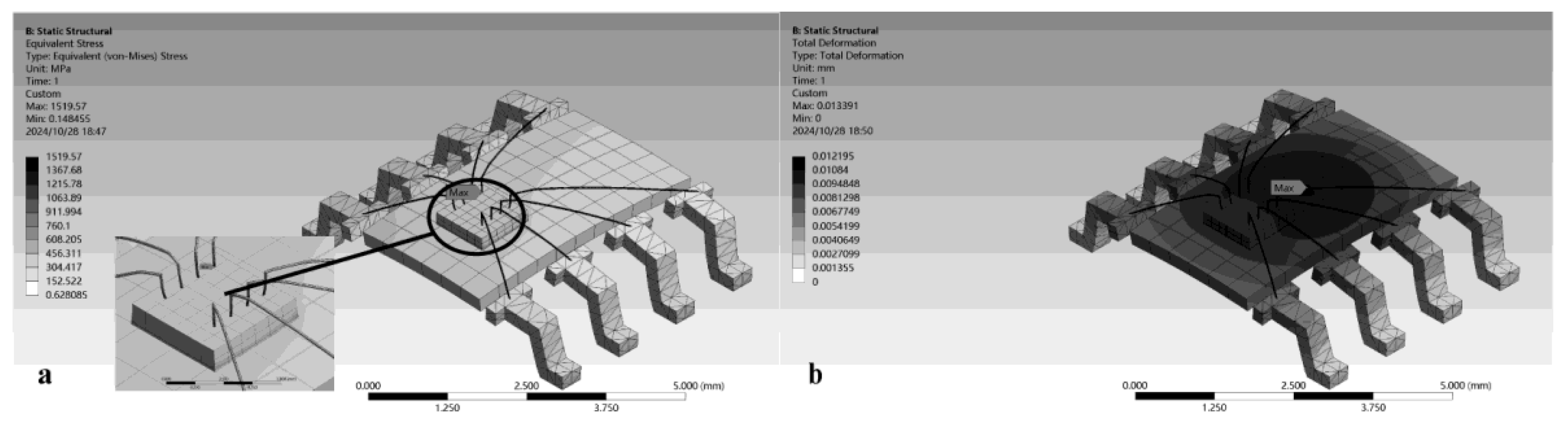
Figure 7a illustrates the internal stress distribution within the sensor. Most areas display stress levels below 50 MPa, effectively dissipating thermal expansion mismatch-induced stresses and maintaining low stress levels. However, a significant stress concentration, exceeding 500 MPa, occurs at the bonding area between the wires and the chip. This area, characterized by geometrical discontinuity, limited contact surface, and considerable differences in the thermal expansion coefficients of the molding compound, bonding wires, and chip material, is prone to stress concentration. Furthermore, solder joints exhibit stresses ranging from 200 MPa to 300 MPa. The pronounced discrepancy in the thermal expansion coefficients between the solder and the chip induces stress concentration. Prolonged or repeated exposure to these high-stress states may result in material fatigue damage, progressive internal crack formation and propagation, and a gradual decline in connection reliability. High stress can also impair the contact characteristics between the gold wires and the chip, leading to increased resistance, diminished signal transmission quality, and other electrical performance issues. Materials subjected to high stress are susceptible to accelerated fatigue damage under persistent or recurrent exposure can precipitate premature performance degradation in critical sensor components. For instance, the mechanical and electrical properties of materials at the bonding area between the gold wires and the chip and at the solder joints may gradually deteriorate due to fatigue damage, increasing the likelihood of sensor failure under normal operating conditions.
As illustrated in Figure 7b, the deformation of the sensor predominantly occurs in the central area of the molding compound and the bonding wires, with a peak deformation of 12.8 µm. In the chip region, the deformation varies between 7 µm and 10 µm. Given the molding compound’s low elastic modulus and high thermal expansion coefficient, it is more likely to deform when subjected to stress. The slender and flexible nature of the bonding wires offers minimal resistance to stretching and bending, rendering them particularly susceptible to pronounced deformation under stress. The interplay between the chip and the adjacent molding compound and gold wires influences the magnitude and distribution of its deformation. The discrepancies in thermal expansion between the chip, the molding compound, and the solder introduce mutual constraints during temperature fluctuations, resulting in a certain degree of deformation that can impact the chip’s performance.

3.3. A novel Magnetic Sensor Packaging Structure with Electromagnetic Shielding and and Wide Temperature Range Adaptability.

As previously noted, in localized high-temperature conditions, the extant magnetic sensor packaging structure displays concentrated stresses surpassing 500 MPa at the bonding interface between the bonding wires and the chip, as well as at the solder joints. This is attributed to the discrepancy in the thermal expansion coefficients of the materials used. Such stress levels pose a considerable risk to both the long-term reliability and the electrical performance of the sensor. Moreover, when subjected to transient strong electromagnetic interference, the current packaging’s capacity for shielding internal electromagnetic fields and managing current densities indicates potential areas for enhancement. To mitigate these challenges, a novel design for the magnetic sensor packaging structure has been introduced.
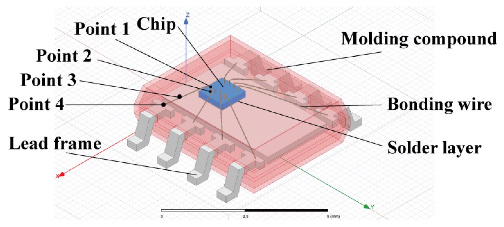
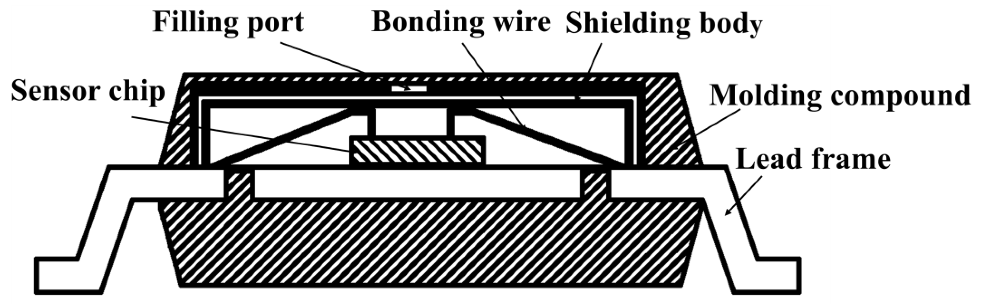
Figure 8 presents the schematic diagram of a novel magnetic sensor packaging structure, comprising the sensor device, bonding wires, shielding body, molding compound, and lead frame. The shielding body, situated externally to the sensor device and bonding wires, is affixed to the lead frame utilizing UV-curable adhesive, which inhibits electrical conduction therebetween, thereby ensuring insulation. This shielding body incorporates an interlayer filled with ferrite powder or alternative electromagnetic shielding powders and is equipped with a powder filling port. Notably, the shielding body is fabricated from a 3D-printed resin. The bonding wires, composed of gold, are welded at one end to the sensor device and at the other to the lead frame. The molding compound, an epoxy material, envelops the exterior of the shielding body, maintaining intimate contact with the lead frame and effectively isolating the sensor device, bonding wires, and shielding body from external environmental influences. The cavity defined by the shielding body serves to segregate the plastic encapsulant material from the bonding wires and sensor device materials, thus mitigating stress and deformation. Manufactured from a copper alloy, the lead frame completes the assembly. The utilization of a 3D-printed resin for the shielding body not only facilitates the formation of an interlayer equipped with a filling port for electromagnetic shielding materials but also broadens the spectrum of feasible electromagnetic shielding materials, thereby offering enhanced electromagnetic shielding for the internal sensor device.
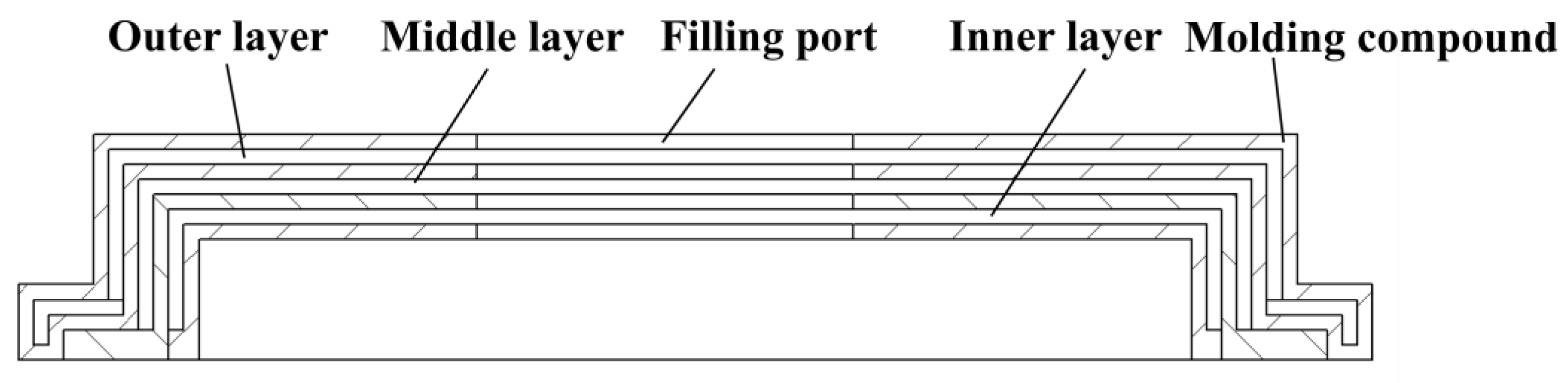
Figure 9 presents a schematic diagram of a multi-layered shielding structure. This structure is designed with each layer filled with a distinct electromagnetic shielding material, resulting in a gradual change in electromagnetic parameters. This facilitates smoother impedance matching and more effective absorption of electromagnetic waves. The structure comprises three layers: an inner layer, a middle layer, and an outer layer, arranged sequentially from the inside out. Each layer is nested one within another and, when combined with the lead frame, forms a closed shielding cavity to safeguard the sensor device and bonding wires. The inner layer, which is nearest to the sensor device, may be constructed from a high-permeability ferrite material. This material effectively guides and confines the magnetic field, providing robust absorption and shielding effects against low-frequency electromagnetic waves. The middle layer employs a transitional material, such as a composite of nickel-zinc ferrite and conductive polymer. Its electromagnetic parameters fall between those of the inner and outer layers, serving to transition and adjust impedance matching. The outer layer is made from a high-conductivity metal material, such as copper or aluminum. Its primary function is to reflect high-frequency electromagnetic waves and prevent the intrusion of external electromagnetic waves. The shielding body can be positioned on both sides of the lead frame. Additionally, the interlayers on both sides can have the same or different numbers of layers and fillers, depending on the desired shielding effects.
In power systems, various application scenarios are subjected to differing intensities and types of electromagnetic impacts. Current molding compound packaging is not specifically tailored for these environments, leading to unavoidable challenges when used in power systems. However, this particular structural design permits a flexible adjustment of the types and ratios of electromagnetic shielding materials, contingent on actual conditions. Whether addressing strong electromagnetic interference near substations or more complex, albeit weaker, electromagnetic environments in power distribution rooms, the shielding solution can be customized accordingly. This ensures effective electromagnetic shielding while also providing economical and practical benefits, thereby reducing costs. Furthermore, power system environments undergo extensive temperature variations, ranging from extreme cold to intense heat. This packaging structure is designed to withstand such a wide temperature range, eliminating the stress and strain caused by thermal expansion mismatches in traditional molding compound packaging. This reduces the risk of sensor failure due to temperature fluctuations, thus extending the sensor’s lifespan and decreasing maintenance costs and replacement frequency.
The innovative packaging structure employs 3D-printed resin to form the shielding body. As of now, 3D printing technology has advanced significantly in material formation, allowing for the fabrication of intricate structures that cater to the design specifications of shielding body interlayers and through-holes. The establishment of a multi-layer electromagnetic shielding structure necessitates meticulous control over the thickness and electromagnetic properties of each layer’s material. Additionally, the adhesion techniques between layers are crucial to ensure optimal impedance matching and electromagnetic shielding outcomes. Research regarding the compatibility and interface management of diverse materials is still ongoing, guaranteeing effective collaboration between layers for efficient absorption and reflection of electromagnetic waves.

4. Discussion

This study utilizes finite element simulation methods to examine the effects of transient strong electromagnetic interference and localized high temperatures on the performance of magnetic sensors. The findings suggest that the electromagnetic field and current density characteristics within the sensor demonstrate a significant temporal correlation with the waveform of the excitation source. For example, as the waveform of the excitation source alters, the distribution of the electromagnetic field and the magnitude and direction of the current density within the sensor also adjust accordingly, exhibiting a certain regularity and synchronization over time. The structural material properties of the sensor play a pivotal role in its anti-interference capability. The appropriate selection of shielding materials can significantly enhance the sensor’s performance. Under localized high-temperature conditions, with an ambient temperature of up to 70°C, thermal analysis via simulated heat transfer and subsequent structural analysis reveal an uneven internal stress distribution within the sensor. Notably, stress concentrations occur at the bonding area between the bonding wires and the chip, as well as at the solder joints, due to factors such as geometric shape, contact area, and differences in thermal expansion coefficients of the materials. These stress concentrations could potentially lead to material fatigue damage, reduced connection reliability, and electrical performance issues. Furthermore, the deformation of the sensor is primarily concentrated in the central region of the plastic encapsulant and the bonding wires, with some deformation also observed in the chip area. The deformation distribution is influenced by various factors, including material properties, structural design, stress, and interactions between components. To mitigate these issues, a new packaging structure is proposed. This structure comprises multiple components, with the shielding body made of 3D-printed resin and filled with ferrite.

Author Contributions

Conceptualization, Guanying Wang and Huaiwen Zheng; methodology, Guanying Wang and Huaiwen Zheng; validation, Guanying Wang, Xianfeng Liang, Ning Zhang and Huaiwen Zheng; investigation, Guanying Wang and Xianfeng Liang; resources, Huaiwen Zheng; writing—original draft preparation, Guanying Wang, Xianfeng Liang, Ning Zhang and Huaiwen Zheng; writing—review and editing, Huaiwen Zheng; visualization, Huaiwen Zheng; project administration, Huaiwen Zheng; funding acquisition, Guanying Wang and Huaiwen Zheng. All authors have read and agreed to the published version of the manuscript.

Funding

This research was funded by State Grid Headquarters Science and Technology Project, grant number 5700-202358704A-3-3-JC” and “The APC was funded by State Grid Headquarters Science and Technology Project, grant number 5700-202358704A-3-3-JC”.

Data Availability Statement

The data presented in this study are available on request from the corresponding author. All simulation models, parameters, and methodologies are described in detail within the article.

Acknowledgments

The authors would like to express their sincere gratitude to Prof. Guofeng Song for his valuable guidance and insightful suggestions during the course of this research.

Conflicts of Interest

The authors declare no conflicts of interest. The funders had no role in the design of the study; in the collection, analyses, or interpretation of data; in the writing of the manuscript; or in the decision to publish the results.

Abbreviations

The following abbreviations are used in this manuscript:
EMI Electromagnetic Interference
VFTO Very Fast Transient Overvoltages
GIS Gas-Insulated Substations

References

  1. Jiang, J.J.; Hu, J.; Ma, G.M.; et al. Application Requirements and Development Trends of Specialized Sensors for Digital Power Equipment [in Chinese]. High Volt. Eng. 2024, 8, 3271–3307.
  2. Cheng, L.; Tao, J.X.; Wu, T.; et al. Research on Internal Electromagnetic Interference in GIS Electronic Transformers [in Chinese]. High Volt. Appar. 2023, 9, 211–218.
  3. Chen, W.J.; Zhao, J.; Bian, K.; et al. Research Progress on Transient Electromagnetic Disturbances Caused by Switching Operations in GIS Substations [in Chinese]. Proc. CSEE 2019, 16, 4935–4948.
  4. Feng, L.M.; Wang, X.B.; Wu, L.Z.; et al. Electromagnetic Disturbance of VFTO on Electronic Transformers in 500kV GIS Substations [in Chinese]. Trans. China Electrotech. Soc. 2016, 1, 85–90.
  5. Wang, N. Research on Electromagnetic Transient Problems Caused by Disconnector Operations in UHV GIS [in Chinese]. Ph.D. Thesis, Shenyang University of Technology, Shenyang, China, 2013.
  6. Zhao, J.; Chen, W.J.; Zhang, J.G.; et al. Analysis of Electromagnetic Compatibility Immunity Requirements for Secondary Equipment in Smart Substations under Switching Transients [in Chinese]. High Volt. Eng. 2015, 5, 1687–1695.
  7. Wang, N.; Lin, X.; Xu, J.Y.; et al. Simulation and Characteristic Analysis of Very Fast Transient Overvoltage in UHV GIS Substations [in Chinese]. High Volt. Eng. 2012, 12, 3310–3315.
  8. Safigianni, A.S.; Spyridopoulos, A.I.; Kanas, V.L. Electric and Magnetic Field Measurements in a High Voltage Center. Ann. Occup. Hyg. 2012, 56, 18–24. [CrossRef]
  9. Kong, X.; Guo, F.; Liang, T.; et al. Measurement and Waveform Characteristics Analysis of VFTO Radiated Electric Field Caused by Breaker Closing on No-Load Transformers in 220kV GIS [in Chinese].Proc. CSEE2016, 18, 5087–5093.
  10. Cao, J.; Wei, M.; Zhou, D. Experimental Study on the Coupling Mechanism of Sensors under a Strong Electromagnetic Pulse. Sensors 2022, 22, 14. [CrossRef]
  11. Liu, Y.; Chai, C.C.; Yu, X.H.; et al. Damage Effects and Mechanisms of GaN High Electron Mobility Transistors under Strong Electromagnetic Pulses [in Chinese].Acta Phys. Sin.2016, 3, 7.
  12. Liang, Q.S.; Chai, C.C.; Wu, H.; et al. Damage Characteristics of CMOS Inverters under Fast-Rising Strong Electromagnetic Pulses [in Chinese]. High Power Laser Part. Beams 2022, 8, 79–87.
  13. Nie, B.W. Correlation between Different Strong Electromagnetic Pulse Parameters and Integrated Circuit Damage [in Chinese]. Ph.D. Thesis, Xidian University, Xi’an, China, 2019.
Figure 1. Structural Diagram of the Simulation Model.
Preprints 151242 g001
Figure 2. Measured Electric Field Interference Values at a 500 kV substation.
Preprints 151242 g002
Figure 3. The variation of electromagnetic field and current density response values over time at various detection points on the chip and bonding wires within the sensor. Figure 3a illustrates the values of the electric field response, Figure 3b depicts the magnetic field response values, and Figure 3c represents the current density response values.
Preprints 151242 g003
Figure 4. The variation of electric field response values over time at various detection points on the chip and bonding wires within the sensor. Figure 4a illustrates the electric field response values at the detection point on the chip. Figure 4b-e depict the electric field response values at detection points 1-4 on the bonding wire, respectively.
Preprints 151242 g004
Figure 5. The variation of magnetic field strength over time at various detection points on the chip and bonding wires within the sensor, both before and after the addition of an external copper shielding layer. Figure 5a illustrates the values of the magnetic field response at the detection point on the chip. Figures 5b to 5e depict the magnetic field response values at detection points 1 to 4 on the bonding wire, respectively.
Preprints 151242 g005
Figure 6. The current density of the detection point before and after the copper shielding layer changes with time. Figure 6a to 6d depict the current density response values at detection points 1 to 4 on the bonding wire, respectively.
Preprints 151242 g006
Figure 7. Internal stress distribution and deformation of the sensor. Figure 7a shows the internal stress distribution of the sensor, Figure 7b shows the deformation of the sensor.
Preprints 151242 g007
Figure 8. Schematic Diagram of the New Magnetic Sensor Packaging Structure.
Preprints 151242 g008
Figure 9. Diagram of multi-layer shielding structure.
Preprints 151242 g009
Table 1. Electromagnetic parameters of each component material.
Relative Permittivity Conductivity (Siemens/m) Relative Magnetic Permeability
Chip (Silicon) 11.9 0 1
Molding Compound (Epoxy Resin) 3.6 0 1
Bonding Wire (Gold) 1 41000000 1
Solder layer (Solder) 1 7000000 1
Lead Frame (Aluminum) 1 38000000 1
Table 2. Thermodynamic Parameters of Materials for Each Component.
Thermal Expansion Coefficient (1/°C) Thermal Conductivity (W/mm·°C) Young’s Modulus (GPa) Poisson’s Ratio
Chip (Silicon) 2.6×10⁻⁶ 0.148 150 0.25
Molding Compound (Epoxy Resin) 6×10⁻⁵ 0.001 3.78 0.35
Bonding Wire (Gold) 1.4×10⁻⁵ 0.315 78 0.42
Solder Layer (Solder) 2×10⁻⁵ 0.048 30 0.4
Lead Frame (Aluminum) 2.32×10⁻⁵ 0.237 70 0.33
Disclaimer/Publisher’s Note: The statements, opinions and data contained in all publications are solely those of the individual author(s) and contributor(s) and not of MDPI and/or the editor(s). MDPI and/or the editor(s) disclaim responsibility for any injury to people or property resulting from any ideas, methods, instructions or products referred to in the content.
Copyright: This open access article is published under a Creative Commons CC BY 4.0 license, which permit the free download, distribution, and reuse, provided that the author and preprint are cited in any reuse.
Prerpints.org logo

Preprints.org is a free preprint server supported by MDPI in Basel, Switzerland.

Subscribe

Disclaimer

Terms of Use

Privacy Policy

Privacy Settings

© 2025 MDPI (Basel, Switzerland) unless otherwise stated