Submitted:
03 March 2025
Posted:
04 March 2025
You are already at the latest version
Abstract
Periodically modulated optical coatings, fabricated by depositing conformal films on modulated substrates, offer unique capabilities for spectral and spatial filtering of light. However, conventional deposition methods often do not achieve the required replication and conformality on submicron-size structured surfaces. In this paper, we compare various thin film deposition techniques, including electron beam evaporation, atomic layer deposition, and ion beam sputtering, to evaluate their ability to control multilayer coating growth on periodically modulated substrates. Our study demonstrates that both single-layer and multilayer coatings produced by ion beam sputtering effectively replicate the initial geometry of structured surfaces, thereby enhancing optical performance.
Keywords:
Coatings
; gratings
; interference lithography
; physical vapor deposition
; atomic layer deposition
; ion beam sputtering
; electron beam evaporation
1. Introduction
The increasing demand for more complex, higher-power, yet smaller optical systems drives the need to advance optical coating fabrication technologies. Therefore, the growing demand for high-quality metamaterials can also be fulfilled by optical coating technologies to form photonic structures for spatial filtering [1,2], polarization control at zero angle of light incidence [3,4], etc. Such structures can be directly applied to increase the performance of microchip or ceramic lasers [5,6].
Current optical coating technologies for laser elements are well-developed for producing high-quality and uniform films on flat or slightly curved substrates. However, modern optical and laser systems increasingly demand optical coatings on complex and structured surfaces. Recent advances in lithography and etching techniques have enabled the fabrication of intricate surface geometries [7,8] that often require dielectric and metallic coatings to achieve functionalities such as polarization control [9], selective absorption [10], and spectral or spatial filtering [11,12]. Therefore, methods are needed to produce coatings that precisely replicate the original substrate geometry. Conventional deposition techniques often face limitations related to coating thickness, as planarization of structured surfaces frequently occurs with increasing film thickness [13].
Additionally, modulation depth introduces distinct challenges: for shallow groove depths, increasing the film thickness flattens the modulation, while for highly corrugated surfaces, excessive coating thickness can lead to crack formation [14,15]. Moreover, different deposition techniques provide varying levels of conformality due to differences in the kinetic energies of deposited atoms. Low energy processes, such as evaporation, exhibit limited surface diffusion, resulting in a porous coating structure. In contrast, higher energy processes, such as ion-assisted deposition or sputtering, lead to denser and more conformal coatings [15].
The autocloning method has been proposed as an alternative for achieving replicatingcoatings on modulated substrates [16]. This technique combines thin film deposition and etching, and it has been applied to produce space-variant optical elements [9,17], spectral filters [18,19], omni-directional [20], high-reflection mirrors [19], etc. However, this process is complex and requires precise deposition and etching parameters optimization. Atomic layer deposition (ALD) is another promising approach. ALD technique is based on gas phase sequential self-limiting surface reactions that enable conformal film growth [21]. It has been applied to coat high-aspect-ratio structures, such as nano-scale holes and trenches [22,23]. Also, such technology is used to form antireflective coatings, thereby enhancing the optical performance and surface qualityof complex micro-optics [24].
The primary aim of this paper is to test several widely used deposition techniques for producing thick (few μm) multilayer coatings on periodically modulated surfaces and to identify the most promising method for nanostructured optical coatings. In this work, we investigated electron beam (E-beam) evaporation, plasma-assisted electron beam evaporation, ion beam sputtering (IBS), and atomic layer deposition (ALD). Initially, we evaluated the replication of the substrate’s surface geometry after the deposition of multilayer coatings using these techniques. Subsequently, the most promising technology to form layers on modulated substrates was investigated in detail.
2. Materials and Methods
2.1. Fabrication of Modulated Substrates
Periodically modulated surfaces were produced by combining laser interference lithography and nanoimprint technology. The fabrication process comprised several steps: (i) preparing a master copy in a photoresist via interference lithography, (ii) fabricating a stamp from the master structure, and (iii) imprinting the master structure onto a substrate using a UV-curable polymer. Laser interference lithography was performed using the third harmonic (355 nm wavelength) of a Nd:YAG nanosecond laser (Ekspla, Lithuania) to create a master grating on the photoresist surface. In our case, an incident angle (θ) of approximately 16 degrees produced a grating periodicity of 600 nm (Figure 1).
The positive photoresist was exposed to a total energy of 0.44 mJ and subsequently developed in a KOH solution. As illustrated in Figure 2 (a), the grating modulation depth varied with the development time, ranging from 350 nm to 50 nm as the time increased from 15 s to 150 s.
The typical grating geometry and transmittance spectra are shown in Figure 2 b) and c), respectively. Gratings with a period of 600 nm and a 200 – 220 nm depth were selected as a suitable substrate structure for further experiments. The master structure was then covered by Ni coating and used in a soft nanoimprint lithography process to fabricate copies using a UV-cured polymer (OrmoComp®, nref = 1.52). Such samples with periodically modulated surfaces are transparent even in the UV spectral range, without low transmittance zones, and indicate sufficient quality for further coating deposition experiments.
2.2. Coatings Deposition Techniques
2.2.1. E-Beam with Glancing Angle Deposition
Electron beam evaporation with glancing angle deposition (GLAD) was employed to produce all-silica multilayer coatings on periodically modulated substrates. This technology is known to be used as a replication method and also in high-power optics fabrication [25]. In these experiments, alternating porous and dense SiO2 layers were deposited at 0° and 70° angles, resulting in effective refractive indices of 1.41 and 1.25, respectively. The substrate was continuously rotated during the deposition. The deposition rate was 3 Å/s and was monitored using a quartz crystal microbalance. In this work, the multilayer coatings were deposited using a Sidrabe system equipped with a stepper motor system for the GLAD method.
2.2.2. E-Beam with Plasma Assistance
Electron beam evaporation with plasma assistance to enhance the kinetic energy of evaporated atoms was used for the deposition process. Multilayer coatings consisting of Al₂O₃ and SiO₂ layers were deposited on structured substrates. Two approaches were tested: one with continuous substrate rotation in a calotte and the other with the stationary sample positioned above the plasma source. No additional heating was used during the process.
2.2.3. Ion Beam Sputtering
Multilayer coatings consisting of Ta2O5 and SiO2 were produced by reactive IBS (total physical thickness was about 2.4 µm). Additionally, in further experiments, 1 µm thick single-layer coatings of HfO2, Ta2O5, Nb2O5 and SiO2 were deposited. Deposition parameters for all single-layer films are summarized in Table 1; no additional substrate heating was used.
2.2.4. Atomic Layer Deposition
Multilayer coating consisting of 17 alternating HfO2 and Al2O3 layers, with individual layer thicknesses of 85,6 nm and 109,4 nm, respectively, was deposited by ALD. HfO2 was grown as a nanolaminate, with an interlayer of Al2O3 inserted after every 186 cycles of hafnia to suppress the crystallization. The precursors used for HfO2 and Al2O3 were tetrakis(dimethylamino)hafnium (TDMAH) and trimethylaluminum (TMA), respectively, with water used as the oxidizer. TDMAH cylinder was maintained at 75 °C. The ALD cycle for HfO2 comprised of 0.2 s TDMAH pulse and 0.02 s of water pulse, with purge durations of 5 s between pulses. ALD cycle for Al2O3 consisted of 0.02 s TMA and water pulses, with purge durations of 5 s between the precursor and oxidizer pulses. Nitrogen was used as the carrier and purge gas at flow rates of 90 sccm and 20 sccm for HfO2 and Al2O3 depositions, respectively. Depositions were carried out at 120 °C using a Veeco Savannah S200 ALD system.
2.3. Characterization
Surface and cross-sectional morphologies of structured surfaces were evaluated using scanning electron microscopy (SEM; Helios Nanolab 650 system) and atomic force microscopy (AFM; Dimension Edge of Bruker system). AFM scan area was 10 µm × 10 µm. Refractive indices and extinction coefficients were determined by OptiChar software (OptiLayer, Gmbh) using transmittance and reflectance spectra measured by spectrophotometry (Photon RT).
3. Results and Discussion
3.1. Investigation of Different Deposition Techniques
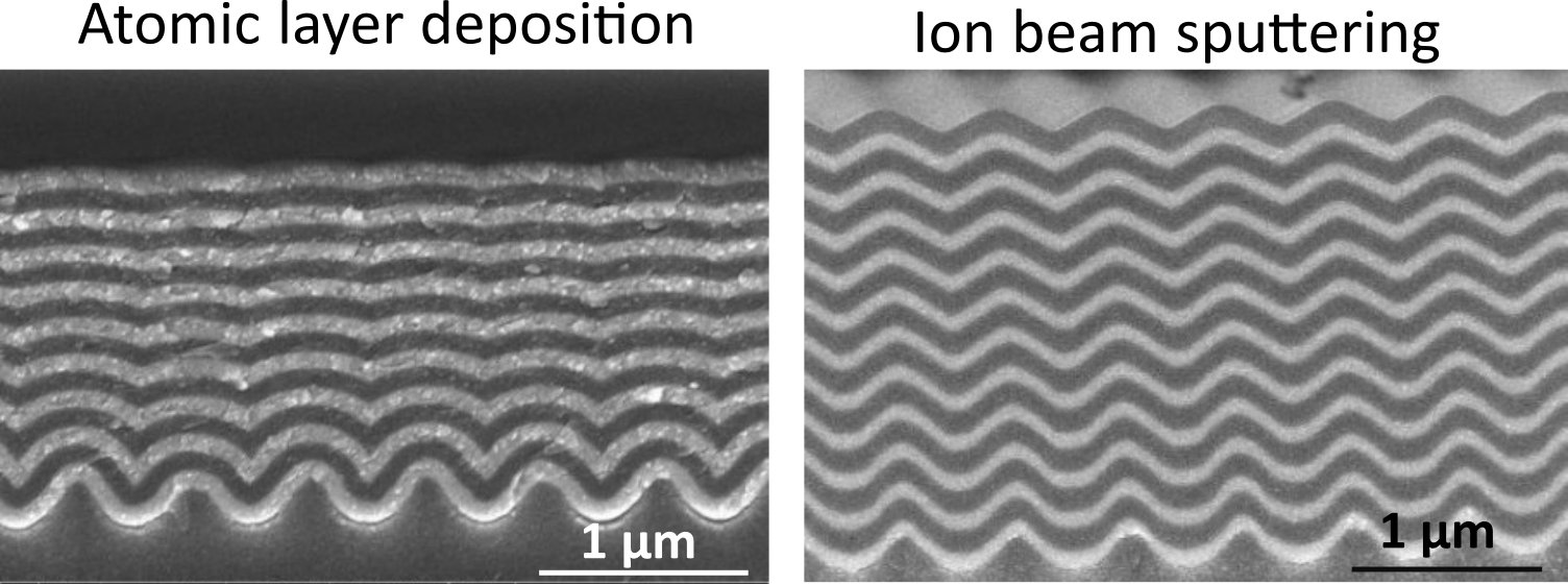
Various thin film deposition techniques were evaluated to produce high-replication of periodically modulated substrates after multilayer coatings fabrication. Thick multilayer coatings (few μ-meters) were deposited using electron beam evaporation with GLAD or plasma assistance, atomic layer deposition, and ion beam sputtering. Cross-sectional SEM images of the coated gratings are presented in Figure 3. For example, using the GLAD method, a 4.5 µm thick multilayer coating reduced the modulation depth significantly from 200 nm to 10 nm (Figure 3 a). This pronounced flattening of the surface can be attributed to the porous coating structure resulting from the low kinetic energy of evaporated atoms. To improve conformality, higher energy deposition techniques with plasma assistance were investigated. However, plasma-assisted e-beam evaporation with substrate rotation also reduced the modulation from 230 nm to 20 nm after depositing approximately 4 µm of multilayer coating (Figure 3 b). In an alternative approach, when the sample was positioned directly over the plasma source without rotation, the modulation depth even increased from 220 nm to 250 nm after depositing a 1.7 µm thick coating (Figure 3 c). However, due to direct exposure to plasma flux, the high process temperature caused by plasma led to significant substrate cracking, indicating potential limitations for producing coatings on sensitive hybrid polymer substrates. All in all, electron beam evaporation with GLAD or plasma assistance seems to quickly planarize the primary surface and only minor modulation can be observed. However, when plasma is used continuously, it leads to sample cracking and cannot be investigated further while using hybrid polymer samples.
Furthermore, the ALD process was investigated for producing multilayer coatings on structured surfaces. Although ALD is known for its conformal growth, as shown in Figure 3 (d), only the first layer accurately replicated the initial surface geometry. Previous studies have reported that when the ALD coating thickness exceeds half of the lateral distance between surface peaks, significant surface smoothening occurs [26,27]. This effect is also evident in Figure 3 (d), where after approximately 1 µm of coating, the surface modulation was largely flattened. Moreover, the ALD coating exhibited high stress and led to substrate cleavage.
In contrast to ALD, the standard IBS method demonstrated the most promising results for coating modulated surfaces. A multilayer coating deposited by IBS on a structured substrate showed a moderate reduction in modulation (from 200 nm to 100 nm) without any substrate damage (Figure 3 e). Similar prelaminar results with replicating IBS multilayer coatings have also been reported in the conference proceedings [15]. Based on these findings, IBS was selected for further investigation.
3.2. Structural Analysis of IBS Single-Layer Coatings
To evaluate the conformality of IBS coatings, single-layer films of various dielectric materials – high refractive index (HfO2, Ta2O5, and Nb2O5) and low refractive index (SiO2) – with thicknesses around 1 µm were deposited on structured surfaces. Surface morphology and geometry were characterized by AFM (Figure 4) and cross-sectional SEM imaging (Figure 5). Modulation depth analysis revealed reductions of 4.5% for HfO2, 3.2% for Ta2O5, and 10% for Nb2O5, with the most significant decrease (35%) observed for the SiO2 layer. Moreover, high refractive index materials maintained a triangular modulation profile, whereas SiO2 exhibited a more rounded morphology.
Since the deposition parameters were based on standard optical coating deposition processes, we further examined the impact of oxygen flow rate on film conformality. As shown in Table 1, the oxygen flow for hafnium oxide deposition is significantly lower than that for other metal oxide films. To determine its effect on coating properties, HfO2 single-layer films were produced using both 5 sccm and 80 sccm of oxygen. Cross-sectional SEM images (Figure 6 a and b) indicate that with 5 sccm of O2, the modulation depth decreased by 4.5%, whereas under oxygen-rich conditions (80 sccm), the reduction was 8.1%.
Additionally, optical properties of HfO2 films deposited on flat fused-silica substrates were evaluated. As illustrated in Figure 6 c) and d), the refractive index at a wavelength of 900 nm decreased from 2.02 with 5 sccm O2 to 1.93 with 80 sccm O2, accompanied by significantly increased optical losses. These results suggest that while oxygen flux influences optical characteristics, it has minimal impact on film conformality.
The more rapid modulation flattening observed with the SiO2 film is likely attributed to its intrinsic chemical properties. Table 2 compares the molecular weights of the pure materials used in depositions. Pure materials are analyzed rather than their oxides since the sputtered atoms are oxidized upon reaching the substrate. Hafnium and tantalum, with higher molecular weights than silicon or niobium, are less easily scattered by residual gas, resulting in denser films and slower modulation smoothening.
3.3. Optical Analysis
Notably, both single-layer and multilayer coatings produced on periodically modulated surfaces are of high interest to the laser community as such structures can provide unique characteristics such as spatial filtering. The spatial filtering effect in nanostructured single-layer coatings arises from Fano-type resonances caused by the excitation of waveguide modes in the film and is explained in detail here [11]. Filtering in nanostructured multilayer coatings can be attributed to photonic bandgaps and have more freedom in the optimization of the electric field distribution, optical characteristics and etc.
The main difference of multilayer coating deposited on planar surface or periodically modulated surface is that in latter case there is an additional level of design complexity. One can reach the periodic distribution of refractive index not in one dimension as in standart interference coatings but in two or three dimensions depending on the substrate. Periodicity initiated from the substrate allows to reach the conditions to excite waveguiding modes, which interact with Fabry-Perot modes and can create additional, different shape, high-reflectance/high-transmittance zones in transmittance maps.
Multilayer coatings based on alternating HfO2 and Nb2O5 layers deposited on planar and modulated surfaces are shown as an example of optical response complexity. The total number of 33 layers deposited on the planar surface serves as interference coating (Bragg mirror) with one prominent high reflection zone for 1250 nm wavelength. The same coating (the same deposition run) fabricated on a substrate with a 600 nm periodic surface modulation can lead to different shapes and positions of high-reflectance zones in transmittance maps. Such resonant “crosses” in transmittance maps allows to form spatial filters for particular wavelengths as the light coming at zero angle of incidence is highly transmitted, and light coming at higher angles is reflected. The theoretical analysis and application of such multilayer structures were analyzed in our group’s previous work [12].
4. Conclusions
A series of experiments were conducted to evaluate various thin film deposition techniques for the replication of modulated submicron surface. Few micron-thickness multilayer coatings were deposited using electron beam evaporation with glancing angle deposition and plasma assistance, atomic layer deposition and ion beam sputtering techniques, and their surface geometries were characterized. Coatings produced via electron beam evaporation with glancing angle deposition rapidly smoothed the surface modulation due to the low kinetic energy of evaporated atoms. Similar results were obtained with plasma-assisted deposition using continuous sample rotation, whereas ion-assisted deposition with the substrate maintained in a stationary position above the plasma source provided highly replicating coatings but introduced substrate damage. Although the atomic layer deposition can produce conformal thin films, thick coatings exhibit significant surface smoothing and can cause substrate cleavage due to high internal stress.
In our experiments, ion beam sputtering has proven to be the most promising technique for producing dense and replicating multilayer coatings on corrugated substrates while maintaining a significant fraction of the initial modulation. Additionally, we demonstrated the difference of surface replication for different single-layer coatings deposited by ion beam sputtering. High refractive index materials (Ta2O5, HfO2 and Nb2O5) provided higher replication with modulation reductions by 3.2%, 4.5% and 10%, respectively, compared to a 35% reduction observed for SiO2 single-layer coating. Moreover, high refractive index structured coatings and multilayer structured coatings can be used as spectral and spatial filtering elements in various laser or photonics systems.
Author Contributions
Conceptualization, supervision, analysis – LG; Ebeam and IBS coatings fabrication – L.G. and S.M; ALD coatings – M.D. and D.A.; measurements – L.G., SEM images – A.S., writing, review and editing – L.G. and D.A. All authors have read and agreed to the published version of the manuscript.
Funding
This work was supported by the PerFIN project from the Research Council of Lithuania (LMTLT), agreement No S-MIP-22–80. Also, from Horizon 2020 ERA.NET-COFUND program project MiLaCo (Project No. S-M-ERA.NET-20-2).
Informed Consent Statement
Not applicable.
Data Availability Statement
Dataset available on request from the authors.
Acknowledgments
We thank Geola Ltd. (Lithuania) for providing plates with photoresist film and to dr. D. Gailevičius from Vilnius University (Lithuania) for soft nanoimprint lithography process to fabricate copies of master structure.
Conflicts of Interest
The authors declare no conflicts of interest.
References
- Wang, P.Y.; Herrero, R.; Botey, M.; Cheng, Y.C.; Staliunas, K. Translationally Invariant Metamirrors for Spatial Filtering of Light Beams. Phys. Rev. A 2020, 102, 013517. [Google Scholar] [CrossRef]
- Lymarenko, R.A.; Gailevicius, D.; Meskelaite, I.; Grineviciute, L.; Peckus, M.; Staliunas, K.; Taranenko, V.B. Super-Collimation by Axisymmetric Diffractive Metamirror. Opt. Lett. 2021, 46, 3845. [Google Scholar] [CrossRef]
- Grinevičiūtė, L.; Andrulevičius, M.; Melninkaitis, A.; Buzelis, R.; Selskis, A.; Lazauskas, A.; Tolenis, T. Highly Resistant Zero-Order Waveplates Based on All-Silica Multilayer Coatings. Physica Status Solidi (a) 2017, 214, 1700764. [Google Scholar] [CrossRef]
- Mireles, M.; Hoffman, B.N.; MacNally, S.; Smith, C.C.; Lakshmanan, S.N.; Lambropoulos, J.C.; Rigatti, A.L.; Demos, S.G. Direct-Write Laser-Assisted Patterning of Form Birefringence in Wave Plates Fabricated by Glancing-Angle Deposition. Optica 2023, 10, 657. [Google Scholar] [CrossRef]
- Plukys, M.; Grineviciute, L.; Nikitina, J.; Gailevicius, D.; Staliunas, K. Enhancement of Brightness in Microchip Laser with Angular Filtering Mirrors. Optics & Laser Technology 2025, 181, 111904. [Google Scholar] [CrossRef]
- Doucet, A.; Beydaghyan, G.; Ashrit, P.V.; Bisson, J.-F. Compact Linearly Polarized Ceramic Laser Made with Anisotropic Nanostructured Thin Films. Appl. Opt. 2015, 54, 8326. [Google Scholar] [CrossRef] [PubMed]
- Liu, R.; Cao, L.; Liu, D.; Wang, L.; Saeed, S.; Wang, Z. Laser Interference Lithography—A Method for the Fabrication of Controlled Periodic Structures. Nanomaterials 2023, 13, 1818. [Google Scholar] [CrossRef] [PubMed]
- Sebastian, E.M.; Jain, S.K.; Purohit, R.; Dhakad, S.K.; Rana, R.S. Nanolithography and Its Current Advancements. Materials Today: Proceedings 2020, 26, 2351–2356. [Google Scholar] [CrossRef]
- Mehta, A.; Brown, J.D.; Srinivasan, P.; Rumpf, R.C.; Johnson, E.G. Spatially Polarizing Autocloned Elements. Opt. Lett. 2007, 32, 1935. [Google Scholar] [CrossRef]
- Sergeant, N.P.; Agrawal, M.; Peumans, P. High Performance Solar-Selective Absorbers Using Coated Sub-Wavelength Gratings. Opt. Express 2010, 18, 5525. [Google Scholar] [CrossRef]
- Grineviciute, L.; Nikitina, J.; Babayigit, C.; Staliunas, K. Fano-like Resonances in Nanostructured Thin Films for Spatial Filtering. Applied Physics Letters 2021, 118, 131114. [Google Scholar] [CrossRef]
- Grineviciute, L.; Babayigit, C.; Gailevičius, D.; Peckus, M.; Turduev, M.; Tolenis, T.; Vengris, M.; Kurt, H.; Staliunas, K. Nanostructured Multilayer Coatings for Spatial Filtering. Advanced Optical Materials 2021, 9, 2001730. [Google Scholar] [CrossRef]
- Balonek, Gregory Coating a Grating Structure Using Various Deposition Techniques 2013.
- J. Oliver Characterization of Multilayer Optical Coatings on Microstructured Surfaces 2014.
- Oliver, J.B.; Kessler, T.J.; Charles, B.; Smith, C. Fabrication of a Continuous-Enfolded Grating by Ion-Beam–Sputter Deposition.; 2015; pp. 483–487.
- Kawashima, T. Autocloning Technology: Fabrication Method for Photonic Crystals Based on Sputtering Process. In Proceedings of the AIP Conference Proceedings; AIP: Erice (Sicily), 2001; Vol. 560, pp. 115–122.
- Srinivasan, P. Design and fabrication of space variant micro optical elements 2009.
- Ohtera, Y.; Onuki, T.; Inoue, Y.; Kawakami, S. Multichannel Photonic Crystal Wavelength Filter Array for Near-Infrared Wavelengths. J. Lightwave Technol. 2007, 25, 499–503. [Google Scholar] [CrossRef]
- Destouches, N.; Pommier, J.-C.; Parriaux, O.; Clausnitzer, T.; Lyndin, N.; Tonchev, S. Narrow Band Resonant Grating of 100% Reflection under Normal Incidence. Opt. Express 2006, 14, 12613. [Google Scholar] [CrossRef]
- Chen, S.-H.; Chen, C.-K.; Huang, Y.-C.; Lee, C.-C. Omni-Directional Reflectors for Deep Blue LED Using Symmetric Autocloning Method. OPT REV 2013, 20, 141–144. [Google Scholar] [CrossRef]
- George, S.M. Atomic Layer Deposition: An Overview. Chem. Rev. 2010, 110, 111–131. [Google Scholar] [CrossRef] [PubMed]
- Atomic Layer Deposition of Nanostructured Materials; Pinna, N., Knez, M., Eds.; 1st ed.; Wiley, 2011; ISBN 978-3-527-32797-3.
- Cremers, V.; Puurunen, R.L.; Dendooven, J. Conformality in Atomic Layer Deposition: Current Status Overview of Analysis and Modelling. Applied Physics Reviews 2019, 6, 021302. [Google Scholar] [CrossRef]
- Astrauskytė, D.; Galvanauskas, K.; Gailevičius, D.; Drazdys, M.; Malinauskas, M.; Grineviciute, L. Anti-Reflective Coatings Produced via Atomic Layer Deposition for Hybrid Polymer 3D Micro-Optics. Nanomaterials 2023, 13, 2281. [Google Scholar] [CrossRef]
- Tolenis, T.; Grinevičiūtė, L.; Buzelis, R.; Smalakys, L.; Pupka, E.; Melnikas, S.; Selskis, A.; Drazdys, R.; Melninkaitis, A. Sculptured Anti-Reflection Coatings for High Power Lasers. Opt. Mater. Express 2017, 7, 1249. [Google Scholar] [CrossRef]
- Myers, T.J.; Throckmorton, J.A.; Borrelli, R.A.; O’Sullivan, M.; Hatwar, T.; George, S.M. Smoothing Surface Roughness Using Al2O3 Atomic Layer Deposition. Applied Surface Science 2021, 569, 150878. [Google Scholar] [CrossRef]
- Gerritsen, S.H.; Chittock, N.J.; Vandalon, V.; Verheijen, M.A.; Knoops, H.C.M.; Kessels, W.M.M.; Mackus, A.J.M. Surface Smoothing by Atomic Layer Deposition and Etching for the Fabrication of Nanodevices. ACS Appl. Nano Mater. 2022, 5, 18116–18126. [Google Scholar] [CrossRef] [PubMed]
- PubChem - an Open Chemistry Database at the National Institutes of Health (NIH). Available online: https://Pubchem.Ncbi.Nlm.Nih.Gov/#query=niobium.
Figure 1.
a) The schematic of a laser setup and b) a real laser set-up for the interference lithography process.
Figure 1.
a) The schematic of a laser setup and b) a real laser set-up for the interference lithography process.

Figure 2.
Measured results of fabricated gratings: a) The depth of the grating modulation dependency on the development time in KOH solution. b) AFM measurements of the typical grating surface, c) the transmittance map (transmission depending on the angle (horizontal axis) and wavelength (vertical axis).
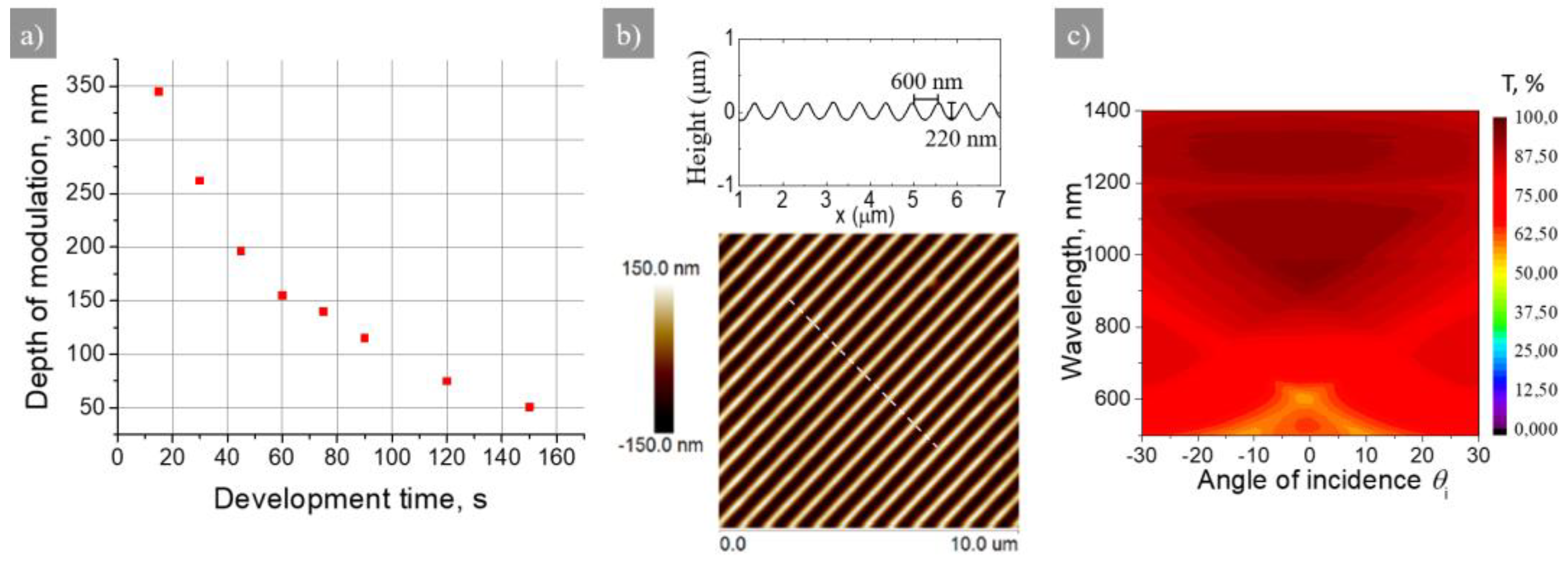
Figure 3.
The deposition of multilayer dielectric coating on a micro-scale corrugated substrate by different technologies: a) e-beam evaporation with Glancing Angle Deposition method (red dashed line marks the interface between the substrate and the coating), b) e-beam evaporation with plasma source when the substrate is rotating in the calotte, c) e-beam evaporation with plasma source when substrate placed stationary above the plasma flux, d) Atomic layer deposition, e) Ion beam sputtering.
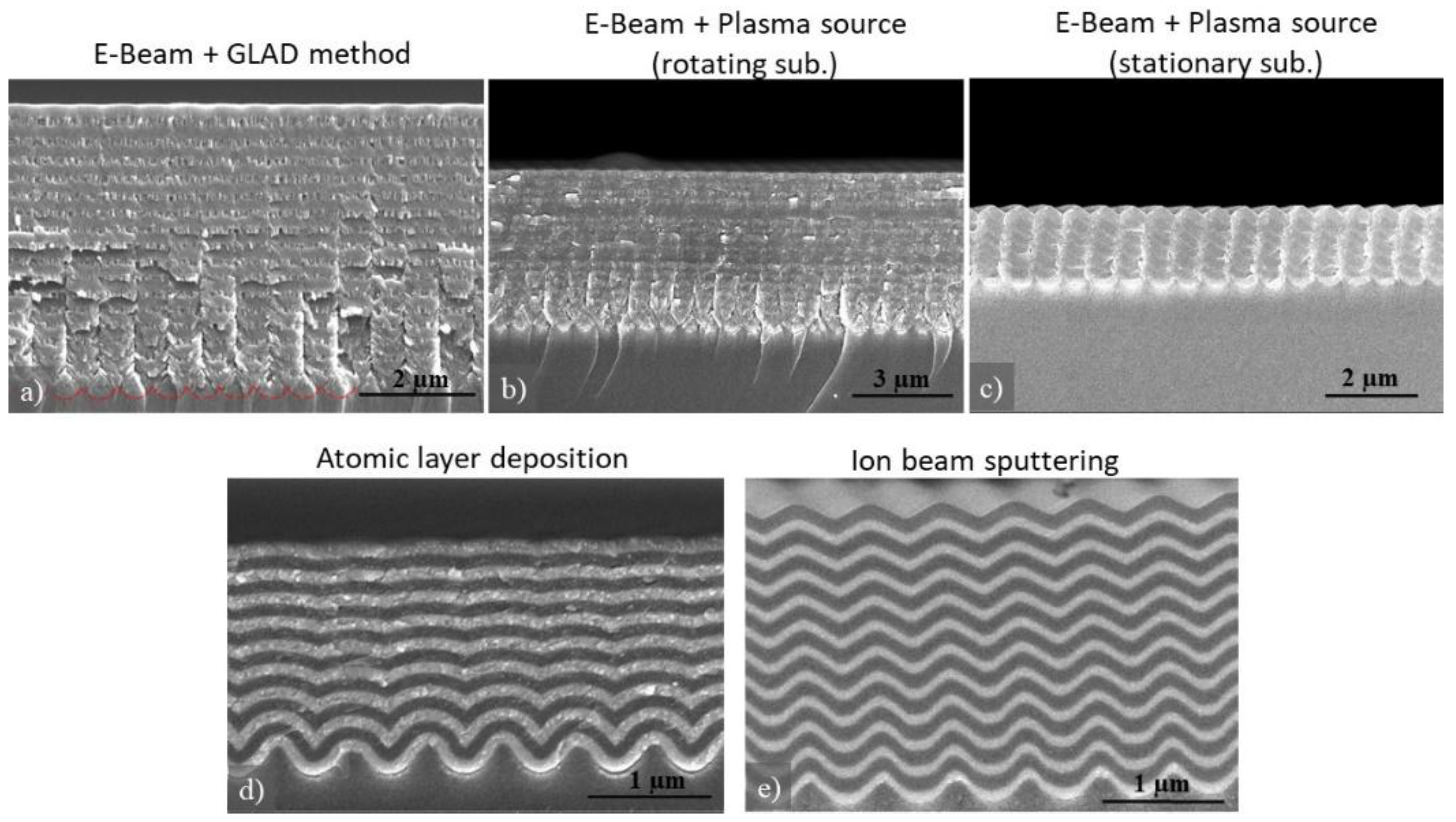
Figure 4.
AFM measurements of single-layer surfaces fabricated from different materials: a) SiO2, b) HfO2, c) Ta2O5, and d) Nb2O5.
Figure 4.
AFM measurements of single-layer surfaces fabricated from different materials: a) SiO2, b) HfO2, c) Ta2O5, and d) Nb2O5.

Figure 5.
SEM images of cross-sections of fabricated single-layers from different materials: a) SiO2, b) HfO2, c) Ta2O5, and d) Nb2O5 materials.
Figure 5.
SEM images of cross-sections of fabricated single-layers from different materials: a) SiO2, b) HfO2, c) Ta2O5, and d) Nb2O5 materials.
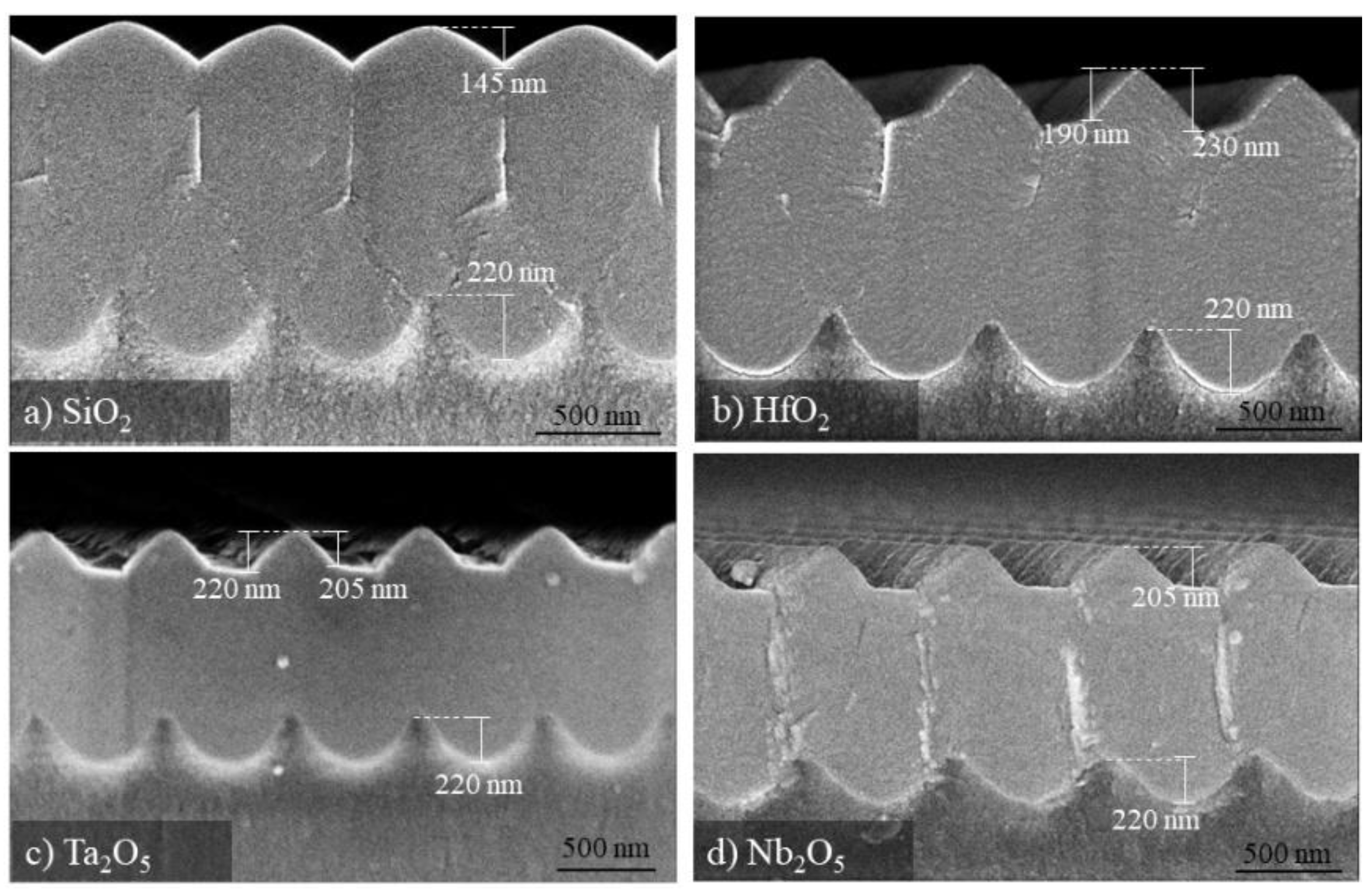
Figure 6.
SEM images of cross-sections of the fabricated samples of HfO2 material by using different amounts of oxygen during the deposition process: a) 5 sccm and b) 80 sccm. c) Refractive index and d) extinction coefficient dispersions of HfO2 layers fabricated using different flow rates of O2 during the deposition process.

Figure 7.
The structural and optical comparison of multilayer structure deposited on planar and modulated surface. SEM images with corresponding transmittance maps of the same HfO2-Nb2O5 multilayer coating deposited on a) and b) flat surface, c) and d) and modulated surface.
Figure 7.
The structural and optical comparison of multilayer structure deposited on planar and modulated surface. SEM images with corresponding transmittance maps of the same HfO2-Nb2O5 multilayer coating deposited on a) and b) flat surface, c) and d) and modulated surface.
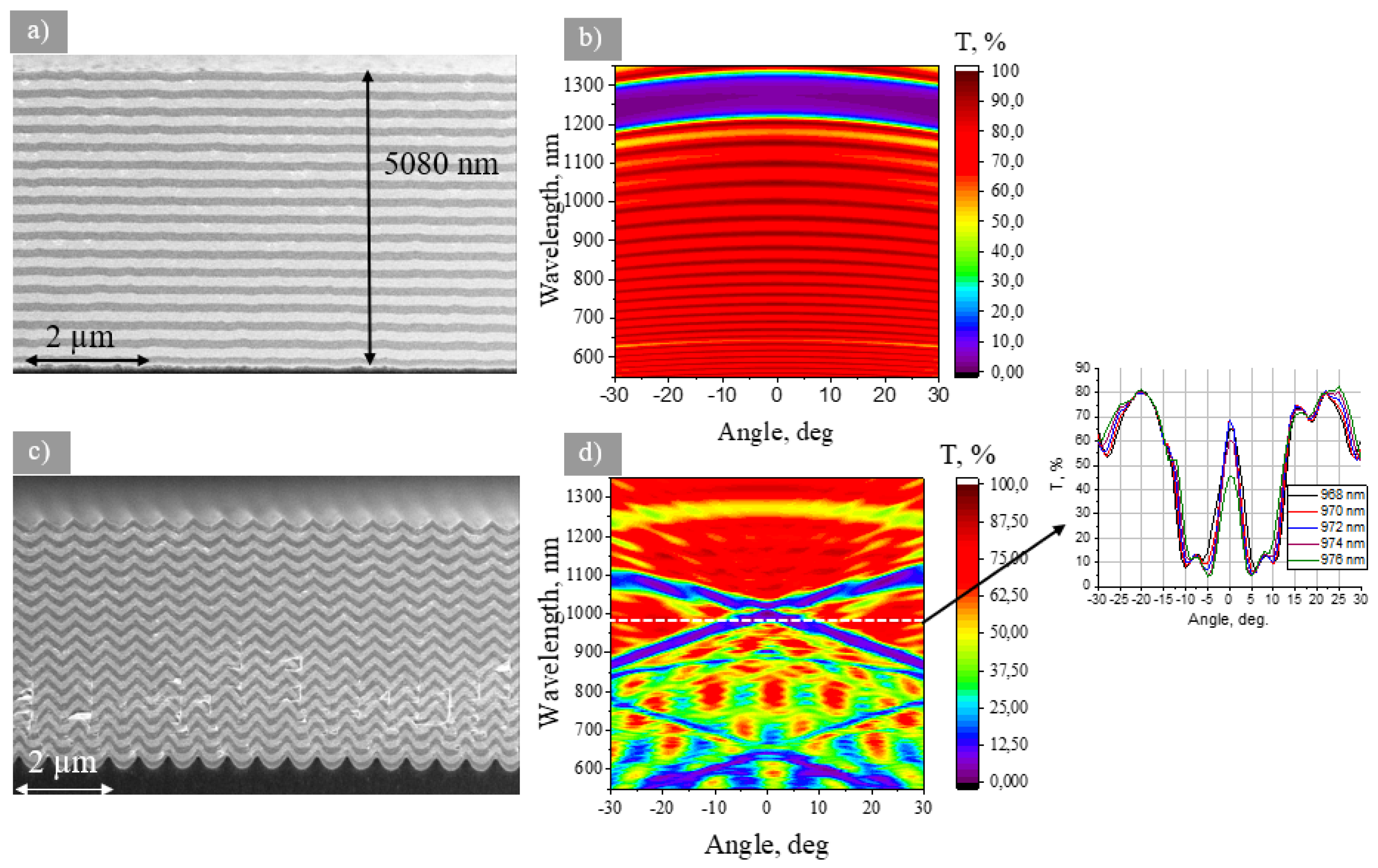

Table 1.
The summarized IBS reactive process parameters for the formation of HfO2, Ta2O5, Nb2O5, and SiO2 single-layer coatings.
Table 1.
The summarized IBS reactive process parameters for the formation of HfO2, Ta2O5, Nb2O5, and SiO2 single-layer coatings.
| Material | Refractive index at λ = 980nm | O2 flux, sccm | Partial pressure, mbar | Physical thickness, nm |
|---|---|---|---|---|
| HfO2 | 2.01 | 5 | 5.0·10-5 | 1000 |
| HfO2 | 1.94 | 80 | 1.4·10-4 | 1000 |
| SiO2 | 1.48 | 80 | 1.4·10-4 | 1000 |
| NbO2 | 2.24 | 80 | 1.4·10-4 | 1000 |
| Ta2O5 | 2.09 | 40 | 8.0·10-5 | 900 |
Table 2.
The molecular weight and density of different materials [28].
Table 2.
The molecular weight and density of different materials [28].
| Material | Molecular weight, g/mol |
|---|---|
| Si | 28.09 |
| Hf | 178.49 |
| Ta | 180.95 |
| Nb | 92.90 |
Disclaimer/Publisher’s Note: The statements, opinions and data contained in all publications are solely those of the individual author(s) and contributor(s) and not of MDPI and/or the editor(s). MDPI and/or the editor(s) disclaim responsibility for any injury to people or property resulting from any ideas, methods, instructions or products referred to in the content. |
© 2025 by the authors. Licensee MDPI, Basel, Switzerland. This article is an open access article distributed under the terms and conditions of the Creative Commons Attribution (CC BY) license (http://creativecommons.org/licenses/by/4.0/).
Copyright: This open access article is published under a Creative Commons CC BY 4.0 license, which permit the free download, distribution, and reuse, provided that the author and preprint are cited in any reuse.


