
Submitted:
25 February 2025
Posted:
27 February 2025
You are already at the latest version
Abstract
In this study, we present the microfabrication process for a surface micromachined accelerometer, aimed at addressing the demand for advanced rehabilitation tools in healthcare. Our overall solution offers an efficient range of motion (ROM) monitoring system to assess upper limb motion, leveraging off-the-shelf components and IoT technology. We focus on the fabrication of a compact wearable prototype, incorporat- ing inertial sensors and a suitable microcontroller for precise angle measurements. This research holds promise for enhancing patient outcomes in physical therapy by providing accurate monitoring and customized rehabilitation exercises through the proposed sensor-measurements in this report.
Keywords:
Micro fabrication
; Poly-MUMPS
; Lithography
; DRIE
; LPCVD
1. Introduction
Progressively increasing the range of motion (RoM) during rehabilitation is crucial to prevent muscle and joint stiffness, maintains or restores flexibility, and helps prevent the formation of scar tissue [1]. Monitoring range of motion (ROM) during rehabilitation can be challenging due to human error, inconsistency, and limited real-time data. Smart sensors could offer access to accurate and objective ROM measurements. They could track progress consistently, identify deviations, and alert therapists to potential issues and open the chance for remote monitoring, progress tracking and providing real-time, data-driven insights to guide and personalize the rehabilitation process [1].
The following demonstration in Figure 1 presents how the sensor will be used and Figure 2 presents accelerometer to be fabricated. It captures the movement data from the body of patient and aligned axis along the body joint for example ankle joint will measure the respective positions between initial point and final point. Moreover, leveraging accelerometer data we also find how fast or slow the patient moves as per the therapist recommendation. Thus, speed, position and joint angle (three) parameters are critical for our application.
2. Pre-Requisites for MEMS
2.1. Selection of Wafer for Our Acclerometer
For MEMS applications, both Si-111 and Si-110 are sutiable for applicaitons [2]. Silicon wafers with a (111) orientation offer moderate mechanical strength, yet they may be susceptible to cleavage along crystallographic planes, potentially compromising their durability. However, they provide excellent control over sidewall angles and etched structures, ensuring precise feature definition critical for motion sensing applications. Despite resulting in smooth surfaces, (111) silicon wafers may necessitate additional structural support to enhance their durability and wearability, making them less inherently suitable for wearable devices without further optimization. In contrast, P-type (110) silicon wafers boast good mechanical strength, being less prone to cleavage and offering stability and support essential for wearable applications. They provide sufficient control over sidewall angles and etched structures, ensuring smooth device fabrication compatible with common micro fabrication processes. P-type (110) silicon wafers are known for their high reliability, being less susceptible to mechanical stress and failure compared to (111) silicon wafers, thus offering long-term performance crucial for wearable device functionality. Consequently, P-type (110) silicon wafers emerge as the preferred choice for wearable applications, providing durability and long-term reliability essential for the seamless integration of wearable devices into everyday life.
2.2. Cleaning Process of Wafer
In our project, we evaluated the properties of Isopropyl Alcohol (IPA) and Hydrogen Peroxide, both commonly used chemicals in semiconductor fabrication processes. IPA, with a chemical formula of CH3H8O, exhibits solubility in water and organic solvents, whereas Hydrogen Peroxide (H2O2) is soluble with water alone. IPA has a boiling point of 82.5°C and is flammable, whereas Hydrogen Peroxide has a higher boiling point of 150.2°C and is non-flammable.
For the cleaning process of our accelerometer, we recommend following the RCA Cleaning Process, comprising three steps. Firstly, RCA-1 Cleaning involves a mixture of concentrated ammonium hydroxide (NH4OH) and hydrogen peroxide (H2O2) in a 1:1 ratio, heated to 70-80°C for 5 to 10 minutes. This step aims to remove organic residues, particles, and some metal contaminants from the P-type (110) silicon wafer. Subsequently, RCA-2 Cleaning utilizes a mixture of concentrated hydrochloric acid (HCl) and hydrogen peroxide (H2O2) in a 1:1 ratio, heated similarly for 10 minutes. This step targets metallic contaminants, native oxide, and other inorganic residues from the wafer surface. Finally, RCA-3 Cleaning involves a deionized (DI) water rinse at room temperature for a few minutes to remove residues of cleaning chemicals and particles from the wafer surface. These cleaning processes are crucial for ensuring the quality and reliability of the accelerometer fabrication process, particularly for P-type (110) silicon wafers.
2.3. Selection of Photoresist for Accelerometer
The selection of photoresist for fabricating comb drive-type surface micromachined accelerometers is a crucial aspect of MEMS (Micro-Electro-Mechanical Systems) device fabrication. We can use negative SU-8 as the preferred choice due to its unique properties compared to other alternatives. SU-8 offers exceptional thickness control, allowing for the deposition of thick layers with high aspect ratios, which is critical for defining tall and narrow features such as comb fingers accurately [3,4]. Additionally, SU-8 demonstrates superior chemical and mechanical stability, ensuring the reliability and durability of the fabricated accelerometers under harsh operating conditions. Its low shrinkage during curing enables precise feature replication and dimensional stability, contributing to the overall performance of the devices. Furthermore, SU-8 is compatible with standard MEMS processes and offers ease of processing, making it suitable for streamlined fabrication workflows. We also propose another alternative as AZ-4562 positive photoresist, used in the lab procedures and it provides uniform coating with specification of upto 30 µm coating thickness. Both the SU-8 and AZ-4562 would be suitable for our fabrication process and accordingly the masks should be designed. The use of negative photoresist SU-8 for fabricating comb drive-type accelerometers would yield better etch line resolution and fulfill the stringent device requirements and guarantees the reliability and performance of the final devices in various applications. On the otherhand, AZ-4562 is provides required exposure resolution for the minimum feature size and considering the compatibility of it, with other process steps based on the lab experience made it as the best choice.
3. Fabrication Flow
3.1. Photomasking and Alignment Marks
In the context of our accelerometer project, global and local alignment marks are critical components employed during the photolithography process to ensure precise alignment and registration of photomasks with the silicon substrate. Given the intricacies of fabricating surface micromachined accelerometers, accurate alignment is paramount for achieving the desired device performance and functionality. Therefore, we have defined our own alignment marks as shown in Figure 3.
Global alignment marks serve as coarse alignment references, typically placed strategically near the wafer edges. These marks enable the lithography equipment to quickly position the wafer in the correct orientation and alignment with respect to the photomask. Given the sensitivity of accelerometer designs to alignment errors, global alignment marks must be designed with high contrast and visibility to ensure robust detection by the alignment system.
On the other hand, local alignment marks play a crucial role in fine-tuning alignment at the die level. Since accelerometers often feature complex structures and high-density arrays of sensing elements, precise overlay alignment between different mask layers is essential. Local alignment marks, positioned within individual accelerometer units or functional areas, provide the necessary fine alignment information to ensure accurate patterning of device features. These marks are meticulously designed to optimize visibility and contrast, particularly in regions of critical device functionality.
3.2. Fabrication Process Steps
The fabrication of surface micromachined accelerometer follows the standard Poly-MUMPS fabrication process where applicable and the simple additive process steps. The process steps are illustrated below with number of steps as (S followed by number) and the choice of specific techniques justified and elaborated. The accelerometer MEMS design has a proof of mass and moving fingers and this whole setup is suspended by the folded beam spring system on either side and anchored to the substrate. The fixed fingers are anchored to the substrate and fixed fingers can be considered as cantilever which are attached to substrate with the small anchors, see Figure 6 and Figure 7. It can be considered that the either side of the spring beams attached to the surrounding polysilicon.
The fabrication flow considers the development of the beams and proof-mass using poly-silicon. For electrical contacts, metal is deposited on the electrodes, which can subsequently be extended to form contact pads. Figure 7 illustrates the cross-section along the electrodes across the proof-mass, corresponding to the vertical line in Figure 6. The fabrication steps are divided into six sections, for the clarity purpose in this report. Each section contains detailed description of the process, materials, and process conditions used.
The p-type Si(111) wafer is the substrate and following the cleaning process mentioned in pre-requisite section, the SiO2 is deposited using LPCVD process at low temperature for the thickness of 2 µm. SiO2 thickness can also be achieved through oxidation process as instructed in lab experiments. The positive photoresist AZ4562 is coated with spin coating to a thickness of 5 um , see Figure 9. The positive photoresist is feasible for this application considering the pattern size of minimum 1 µm. Once the photoresist is exposed with UV light utilizing lithography machine with the mask designed for anchors (Mask-Anchors), the un-exposed resist is removed using KOH developer.
The Si substrate is doped with Phosphorous by diffusing POCl3 on substrate surface, see Figure 8. The doping process yield the resistivity increase and the growth of Si3N4 provides the electrical isolation between the polysilicon and substrate.
To etch the oxide layer, a positive photoresist is used as a mask during the DRIE etching process, which removes the oxide and exposes the substrate. The photoresist is then stripped away in a solvent bath. Next, a total thickness of 7 µm polysilicon is deposited using the LPCVD process, filling the etched oxide areas and forming a 5 µm thick polysilicon layer over the sacrificial oxide layer. An additional PSG layer is deposited on top of the polysilicon as a sacrificial layer. The wafer is then annealed at 1050 °C for 60 minutes to reduce residual stress in the structure, as shown in Figure 10.
The wafer is cleaned again before coating the photoresist as described above for a thickness of 5 µm in order to pattern the microstucture of accelerometer which includes Proof-mass, fingers, electrodes and folded spring beams. For the lithography, the second mask (Mask - beams and structure) used following the same procedure as in earlier section. The unprotected photoresist is removed with KOH developer and using the photoresist as mask, the RIE process used to etch the PSG layer and poly-silicon (Poly0), see Figure 11. The photoresist and PSG masks stripped using diluted HF.
After removing the photoresist mask and cleaning, a second oxide layer is deposited on top of the microstructure as the initial step for metal deposition. A total thickness of 7 µm of SiO2 is deposited using the LPCVD process. The photoresist is then spin-coated to a thickness of 5 µm, and the lithography process is carried out using the third mask for metal deposition (Mask - Metal), as shown in Figure 12.
The un-protected regions of the photoresist which correspondence to metal areas removed with KOH developer and following the wafer cleaning process, the Silicon di-oxide layer is etched by reactive ion-etching (RIE) process with photoresist as mask.Here, the metal deposition need to be done on the beams which act as electrodes only, thus as per the mask the middle structure will be deposited with metal as shown in Figure 13. The selectivily of oxide and photoresist using RIE is around 1.5 and considering the 2 µm thickness of oxide and 5 µm thickness of PR, it is feasible. The wafer is cleaned with ultrasonic before placing into the thermal sputtering chamber to deposit adhesion layer of gold for 5 nm followed by the Al deposition. For the metal deposition a lift-off profile is used to break the continuity with photoresist layer, see Figure 13.
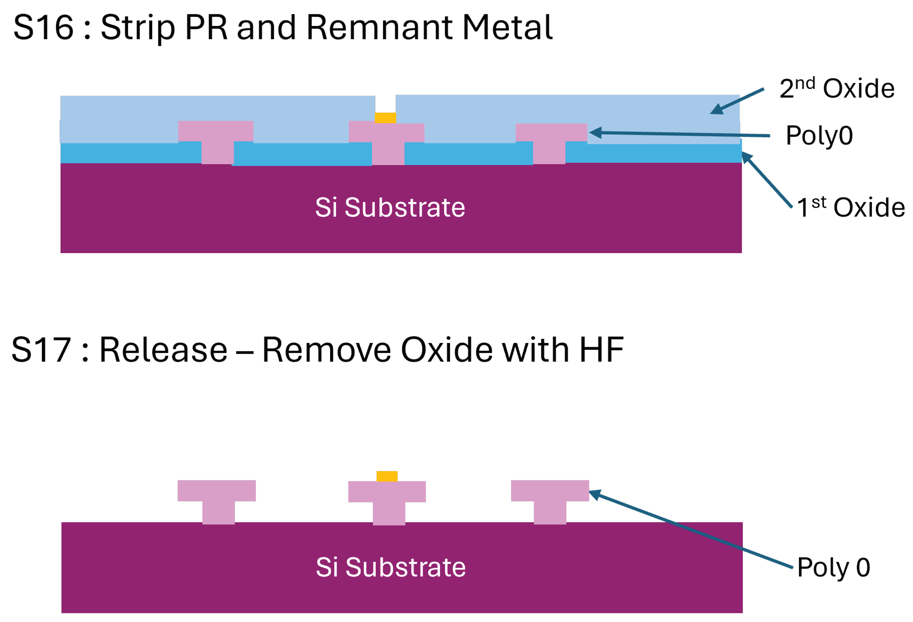
The photoresist and remnant metal is stripped by rinsing in HF solvent and it is ready for the release process. The releasing process is critical as the fingers and the proof-mass are vulnerable to stiction phenomena and an elaborated release process step followed. The wafer is immersed in 49% HF for 5 minutes to release the microstructure and then cleaned with DI water by soaking in it and followed by Isopropyl alcohol solution, see Figure 14 [5]. The wafer transferred to methanol and supercritical CO2 drying is carried out at 31.1°and 1073 PSi [5]. Here, the liquid CO2 displace methanol within the structure at supercritical stage and with the raise in temperature the carbondioxide turns into gas with lower surface tension effect and thus effectively avoid the stiction problem.
4. Conclusion
In this work, a microfabrication process flow is described to fabricate a surface micromachined MEMS accelerometer, which will be used in measuring the Range of Motion (ROM) for upper limb monitoring devices in healthcare applications. The manufacturing process starts with selecting the optimal silicon wafer and ends with the release of the microstructure. P-type (110) silicon wafers are chosen for their reliable base, offering the mechanical strength and stability necessary for wearable devices. RCA cleaning procedures and strategies for selecting light-resistant materials helped achieve the precise design elements needed for motion sensing. The development process is divided into six categories, each of which contributed to a number of device designs. The scalability and mass production potential of this device has been demonstrated.
References
- “Range of motion sensors for monitoring recovery of total knee arthroplasty,” 2022.
- “What is the orientation of silicon wafer 100, 111, 110?” Oct 2018. [Online]. Available: https://www.universitywafer.com/silicon-orientation.html.
- Z.-C. Geng, Z.-F. Zhou, D. Hui, and Q.-A. Huang, “A 2d waveguide method for lithography simulation of thick su-8 photoresist,” Micromachines, 2020.
- E. Laforge, R. Anthony, P. McCloskey, and C. O’Mathuna, “A thick photoresist process for high aspect ratio mems applications,” 2016.
- K. Wang, “Module 6: Surface micromachining technology 1,” 2024, lecture Slides, 2024 Spring MFA 4000 L0308.
Figure 1.
Pateint using the wearable device.
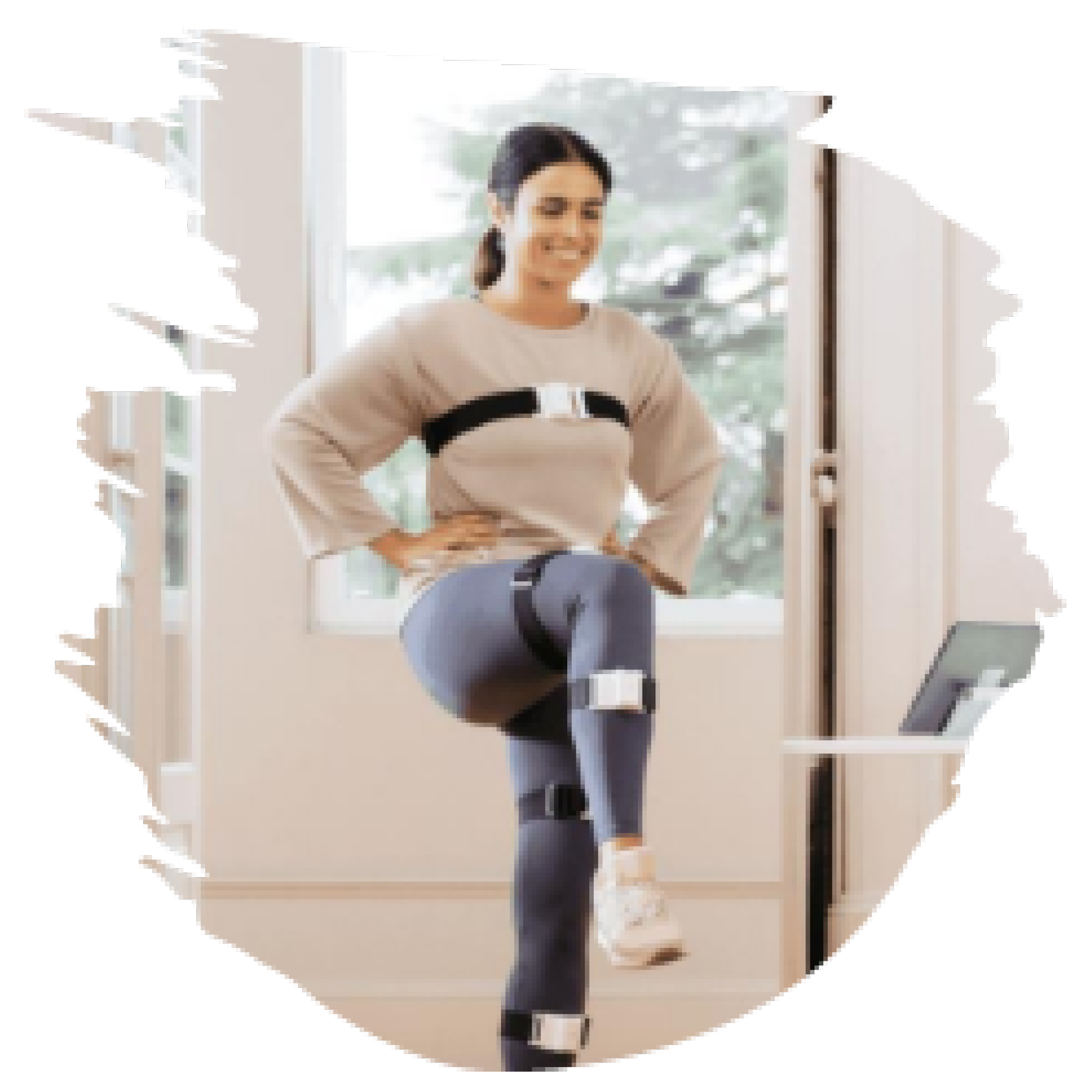
Figure 2.
Acclerometer Fabricated - 3D View
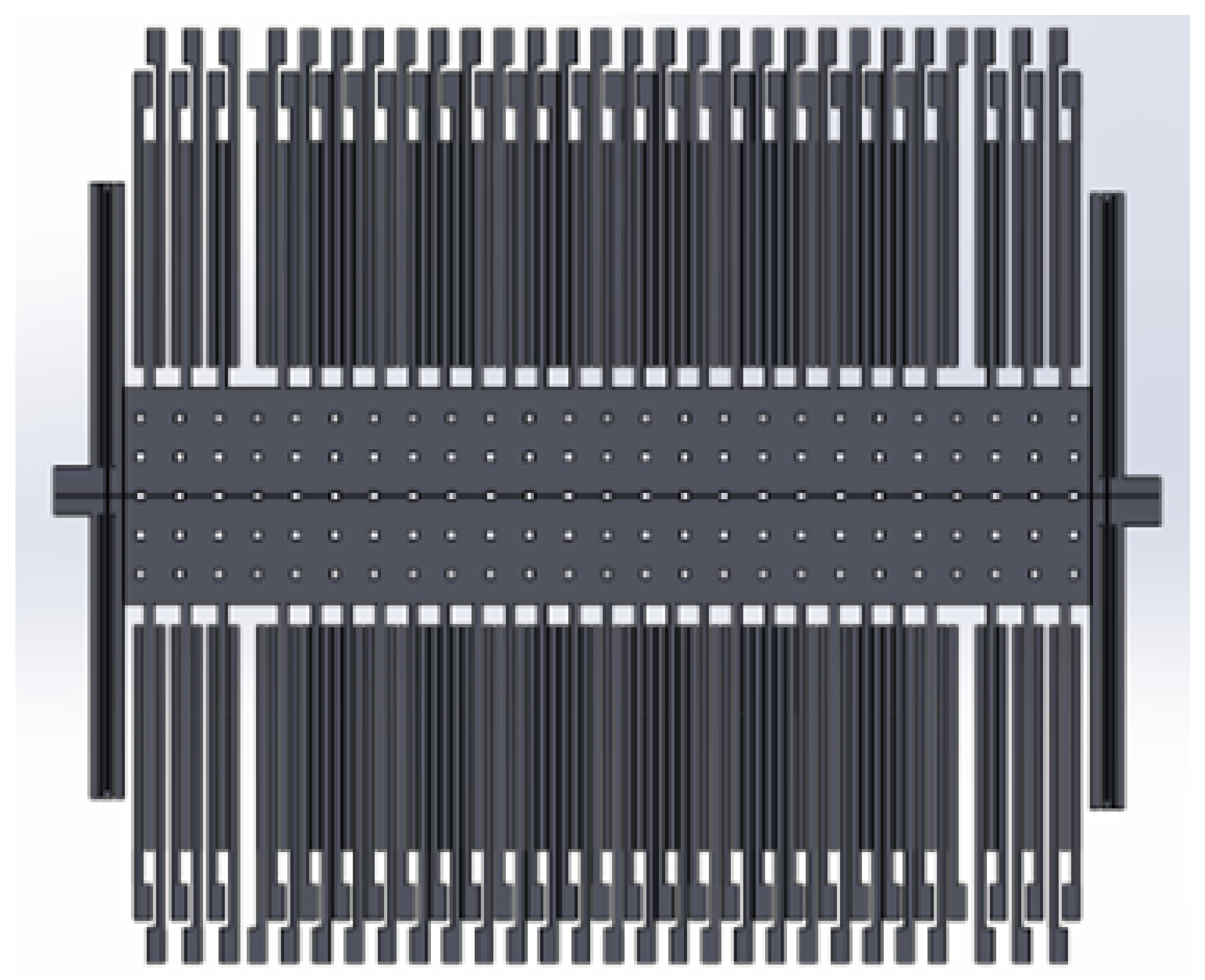
Figure 3.
Accelerometer Dimensions and Alignment Marks Setup
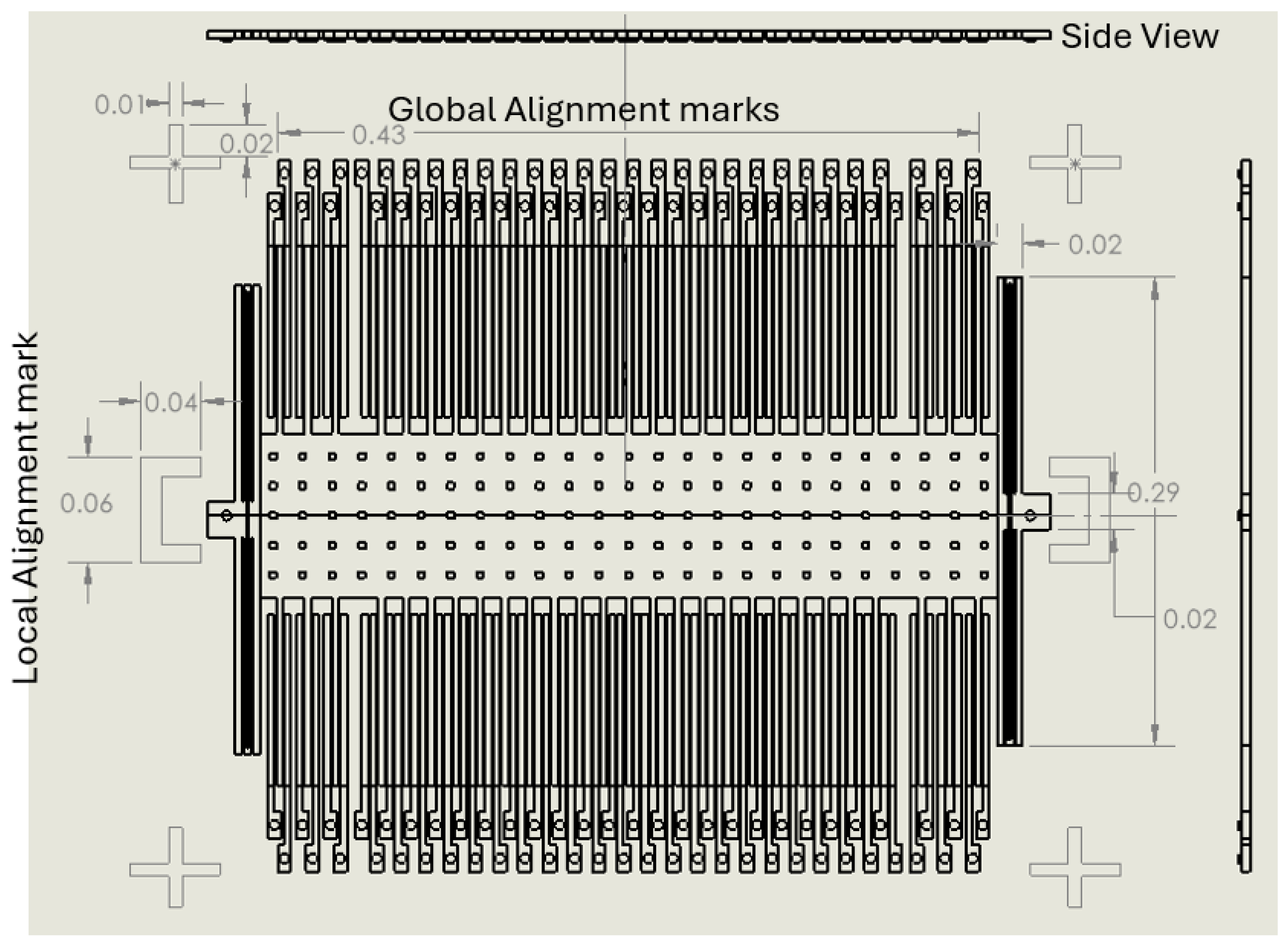
Figure 4.
Photomask Slicing Layer 1
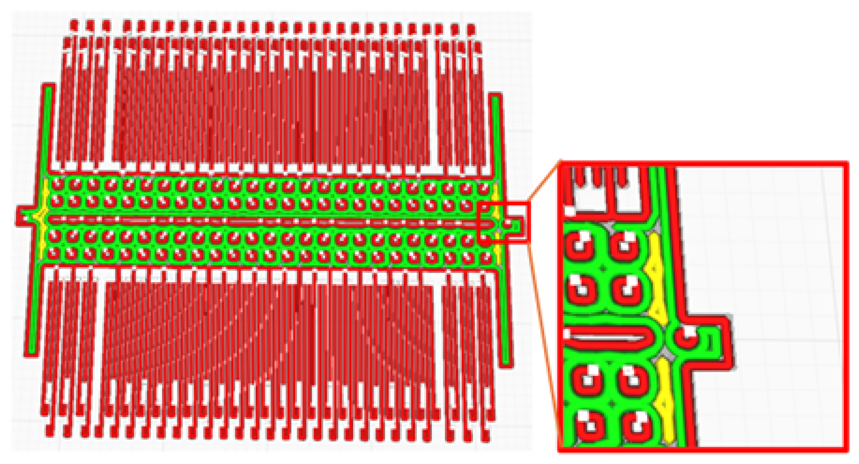
Figure 5.
Photomask Slicing layer 2
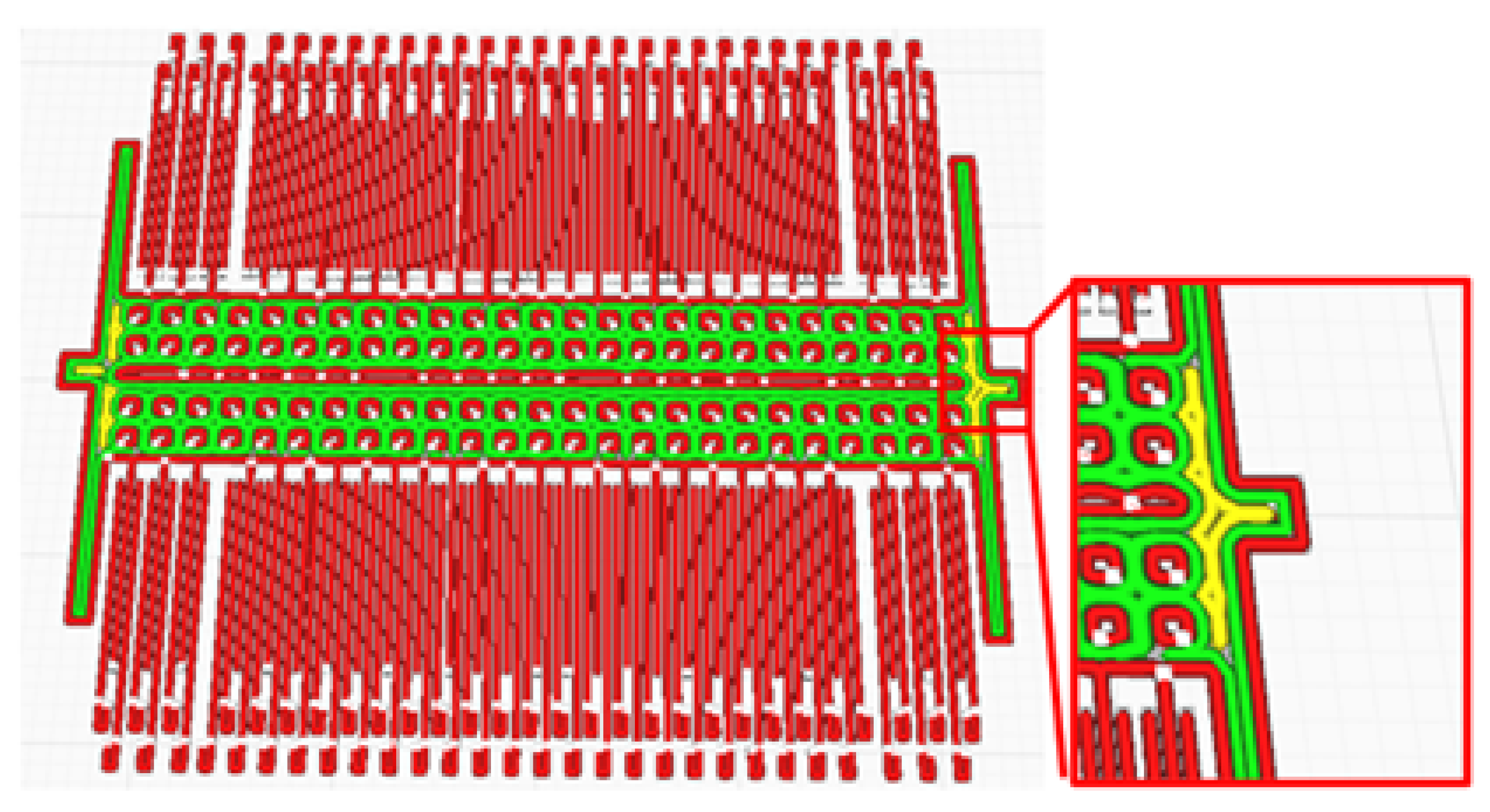
Figure 6.
Accelerometer with Anchor Points
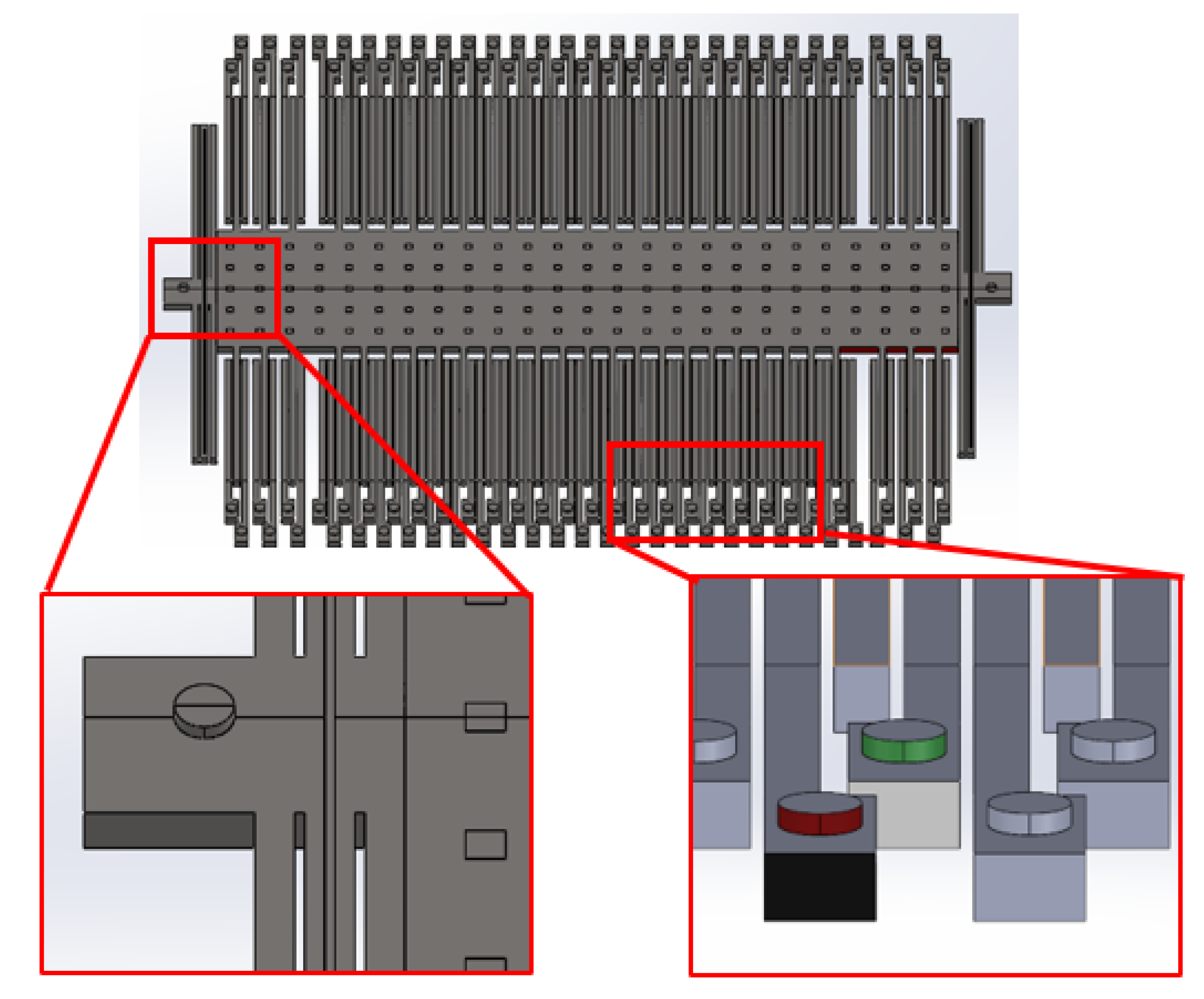
Figure 7.
The illustration of the fabrication cross section which is described in the flow
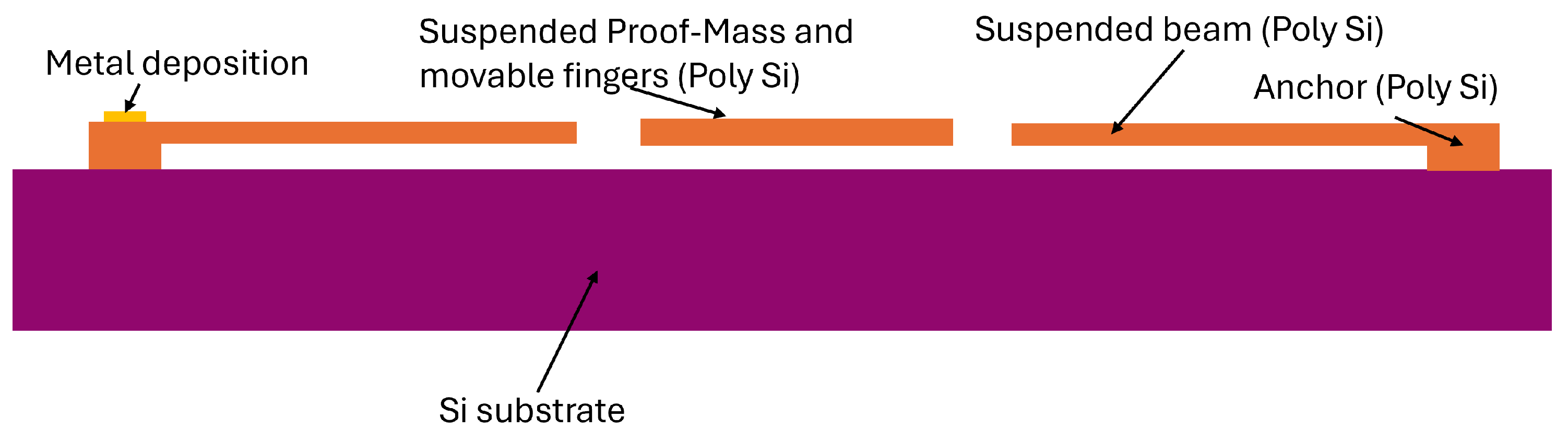
Figure 8.
The illustration of the wafer treatment by diffusing POCl3 and grow Si3N4 layer for adhesion
Figure 8.
The illustration of the wafer treatment by diffusing POCl3 and grow Si3N4 layer for adhesion
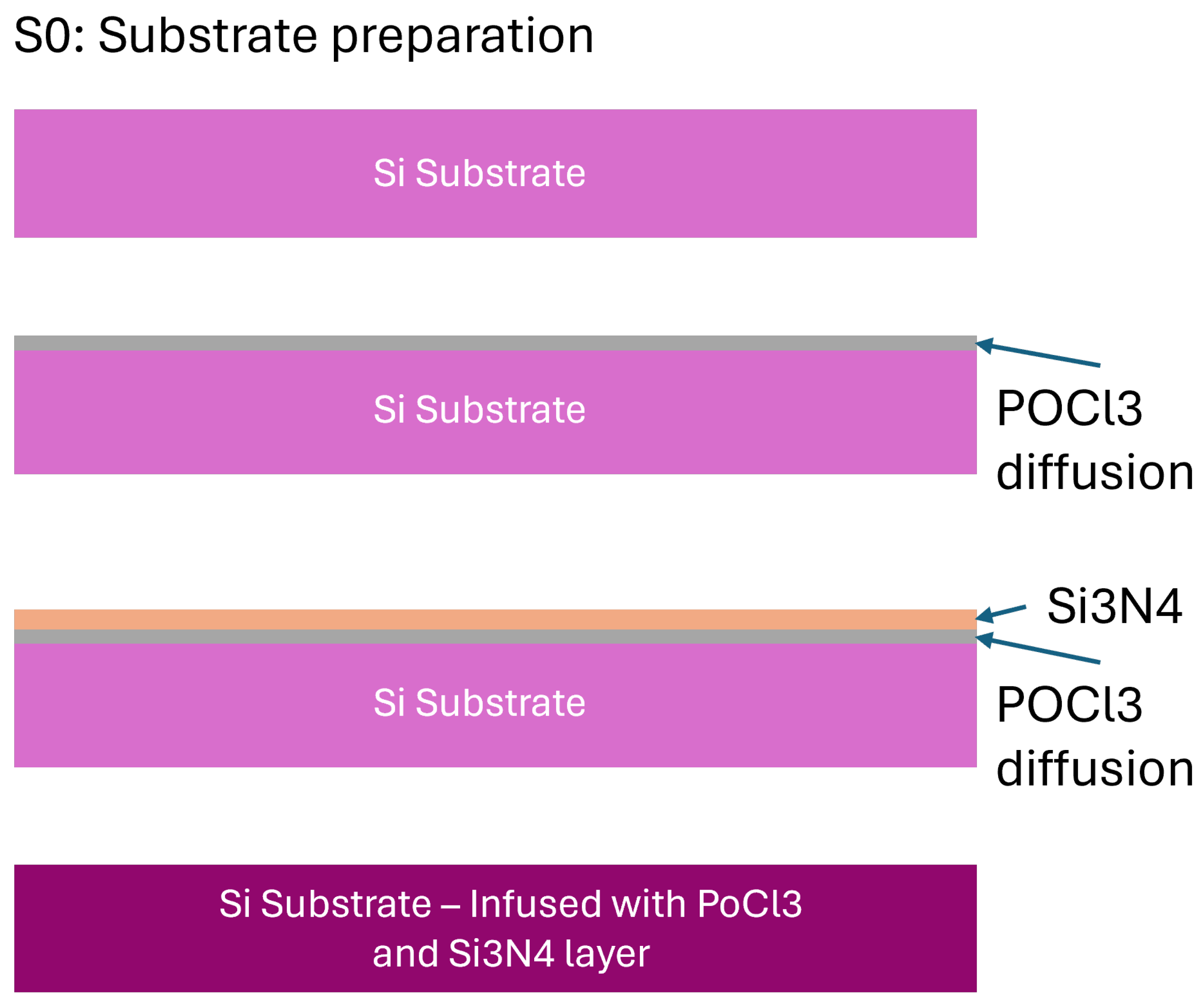
Figure 9.
The illustration of the fabrication flow - Section 1
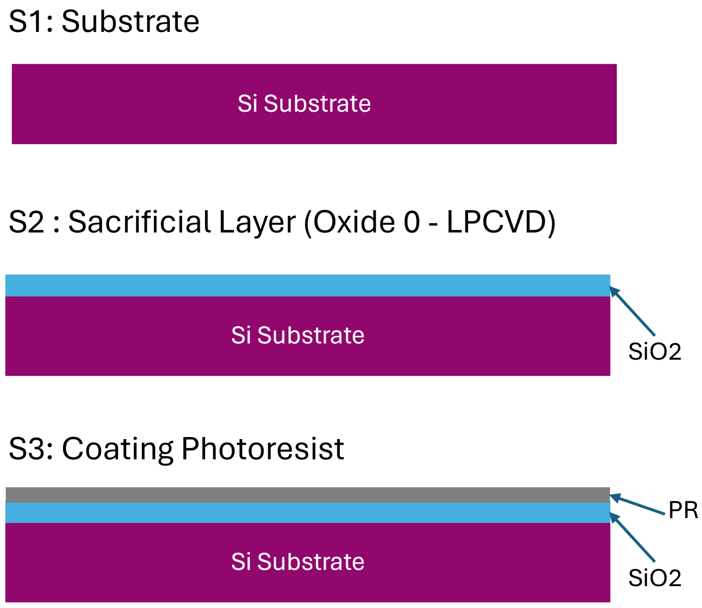
Figure 10.
The illustration of the fabrication flow - Section 2
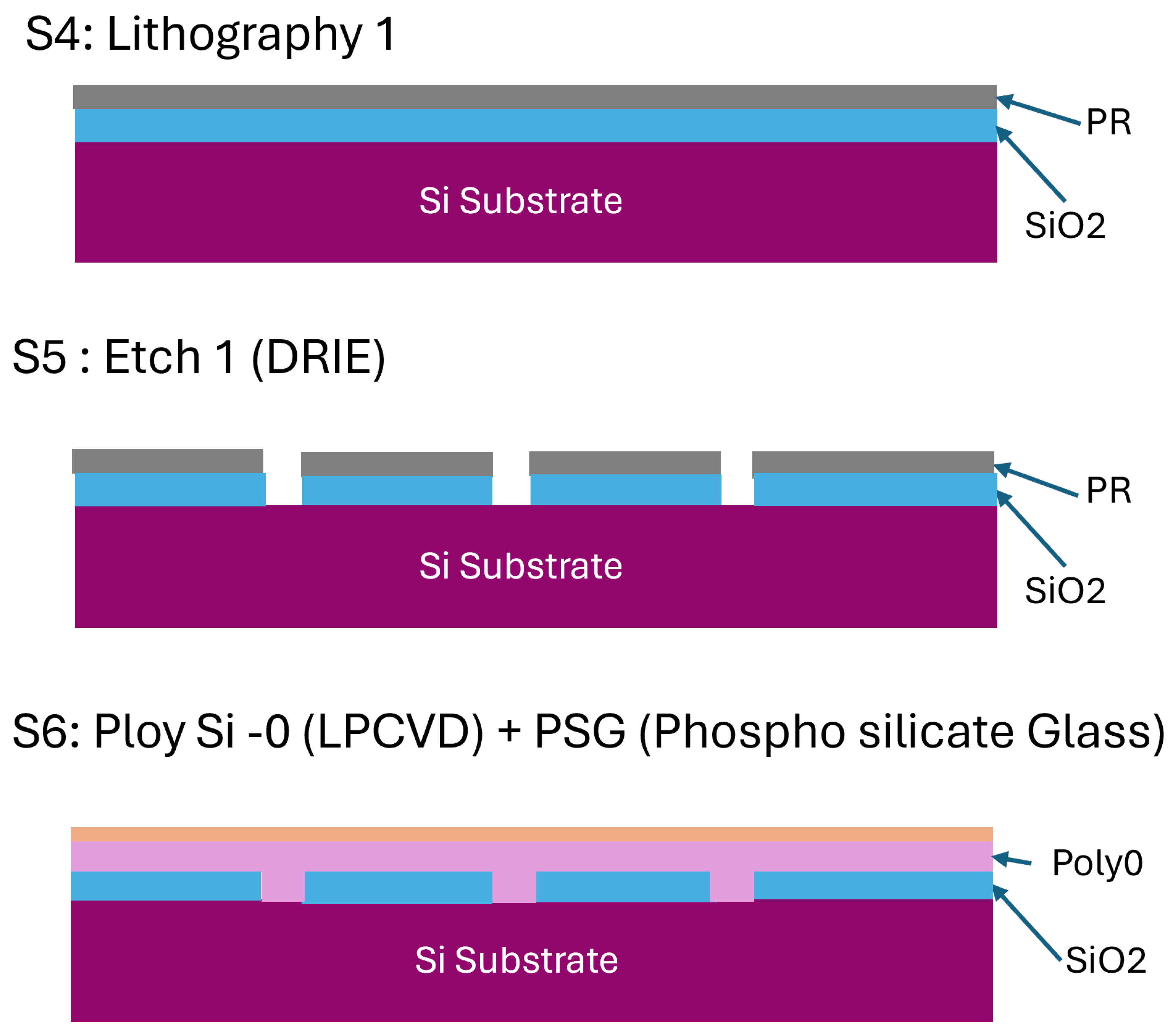
Figure 11.
The illustration of the fabrication flow - Section 3

Figure 12.
The illustration of the fabrication flow - Section 4
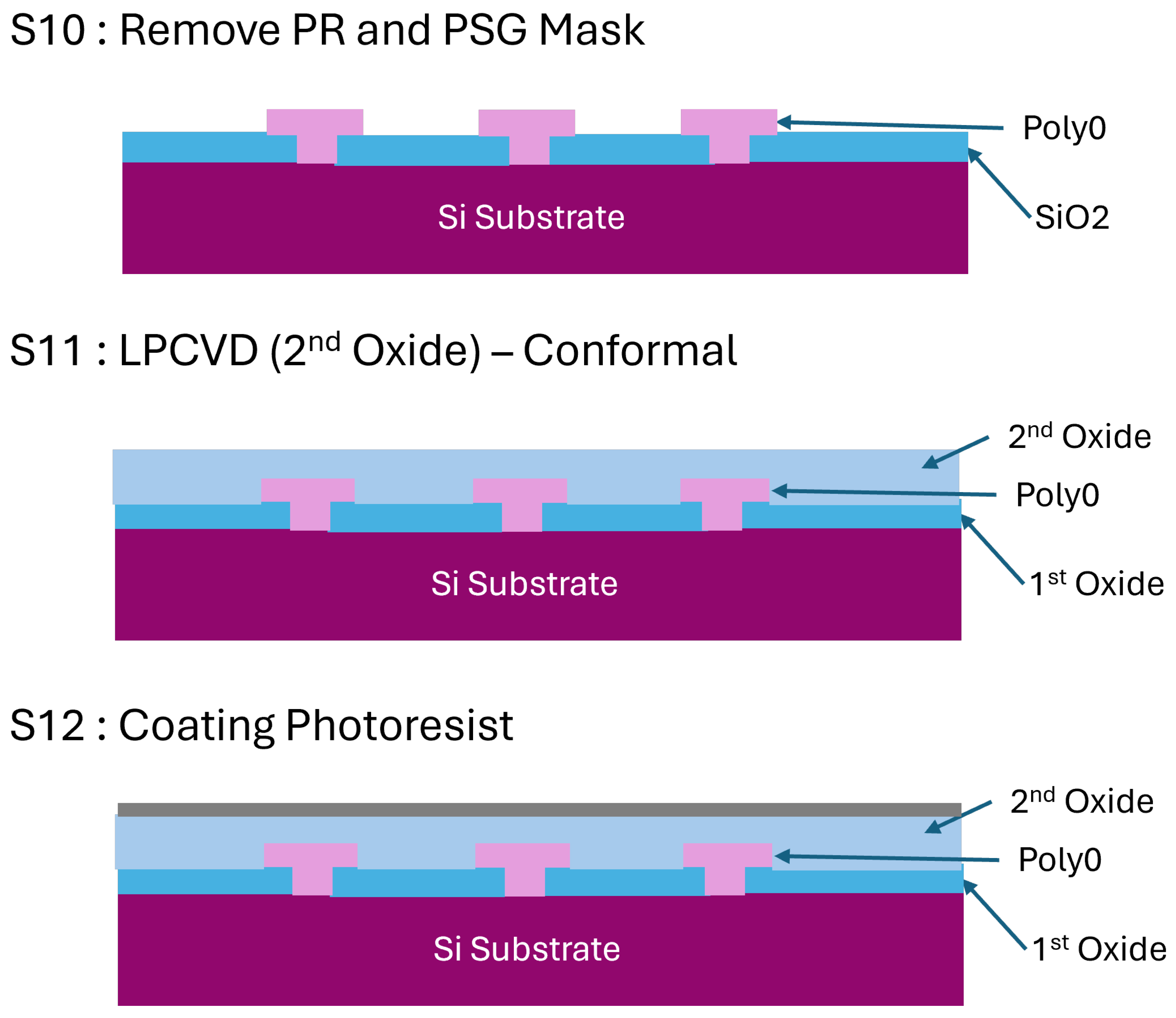
Figure 13.
The illustration of the fabrication flow - Section 5
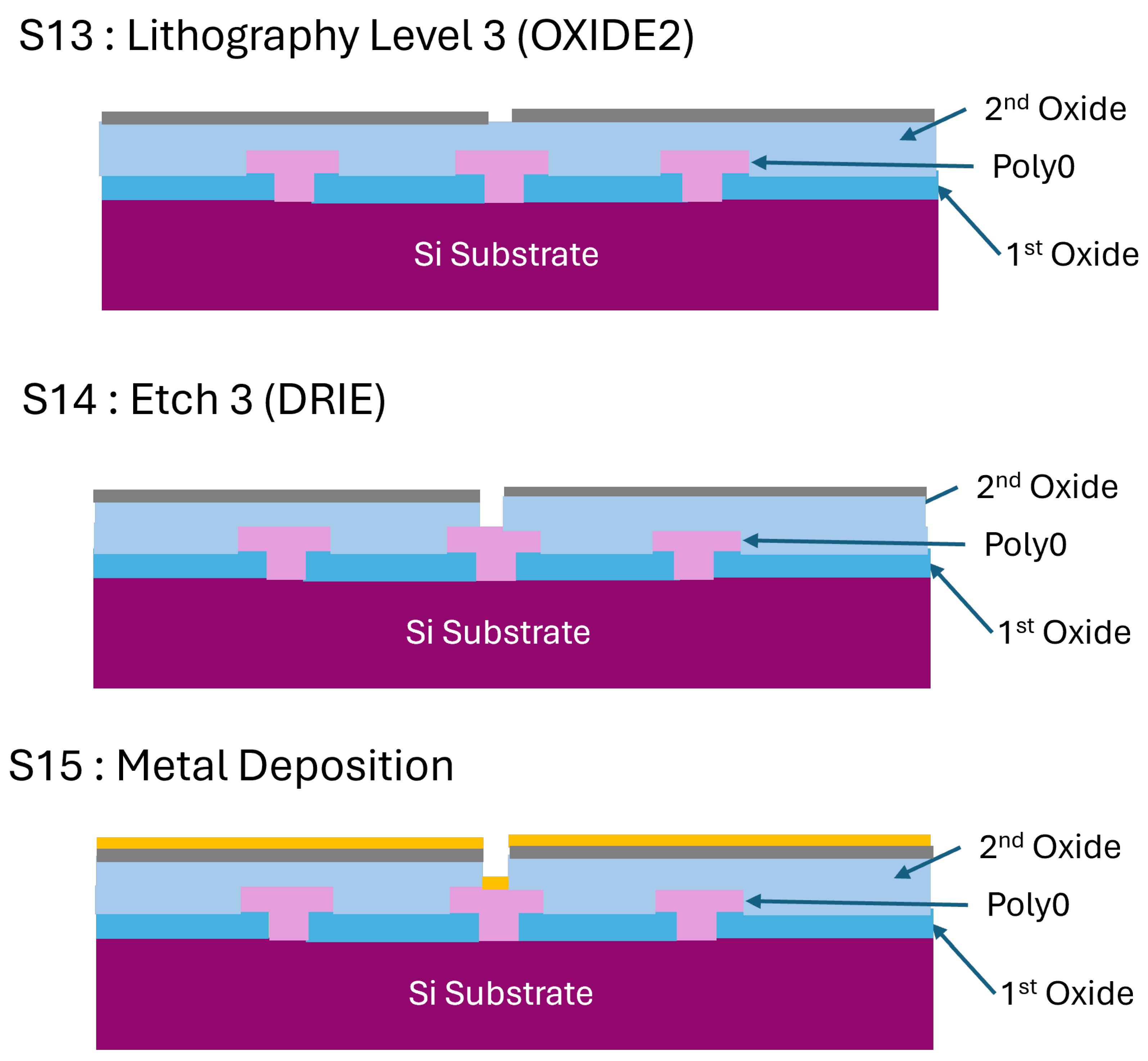
Figure 14.
The illustration of the fabrication flow - Section 6
Disclaimer/Publisher’s Note: The statements, opinions and data contained in all publications are solely those of the individual author(s) and contributor(s) and not of MDPI and/or the editor(s). MDPI and/or the editor(s) disclaim responsibility for any injury to people or property resulting from any ideas, methods, instructions or products referred to in the content. |
© 2025 by the authors. Licensee MDPI, Basel, Switzerland. This article is an open access article distributed under the terms and conditions of the Creative Commons Attribution (CC BY) license (http://creativecommons.org/licenses/by/4.0/).
Copyright: This open access article is published under a Creative Commons CC BY 4.0 license, which permit the free download, distribution, and reuse, provided that the author and preprint are cited in any reuse.


