Submitted:
25 February 2025
Posted:
26 February 2025
You are already at the latest version
Abstract
A high-efficiency frequency multiplier is presented in 65-nm CMOS with a core area of 0.06 mm2. A low-cost five-segment triangular-resistance phase interpolation scheme is proposed. By performing resistive interpolation on four-path orthogonal triangular signals, 10-fold frequency multiplication is achieved within the input frequency range of 12-20 MHz. The prototype only includes a quadrature square-wave generator, four orthogonal square-triangular converters, and the proposed four-path five-segment triangular-resistance phase interpolators, with the acceptable frequency deviation. The presented design achieves an output power of -9.8 dBm, with an input power of -2.0 dBm and the power consumption of 0.45 mW from a 1.2-V supply, which obtains a frequency multiplication efficiency up to 9.6%. The proposed mechanism could be extended to accomplish a configurable multiplication factor.
Keywords:
frequency multiplier
; triangular-resistance phase interpolation
; high efficiency
; configurability
1. Introduction
Frequency multipliers are widely utilized in communication systems to generate high-frequency working clocks from a low-frequency reference one. The traditional mechanisms for achieving frequency multiplication can be broadly divided into two categories. One is to use a nonlinear device or a narrow-pulse generator for harmonic generation and then employ a bandpass filter to extract the desired harmonic frequency [1,2,3,4], but encounters a limited multiplication factor or a complex filtering topology. The other is to use digital sub-sampling / injection-locked phase-locked loops (PLLs) based on frequency discrimination and division, to get a higher output frequency from the embedded voltage-controlled oscillator (VCO) under the reference of a lower input frequency, which has a pure output spectrum and low output noise, at the cost of the hardware implementation [5,6,7].
An optimized method is to inject the harmonics into a free-running oscillator or quadrupler [8,9], however, the injection-locked frequency multipliers suffer from a limited frequency range, and additional error-correcting modules are required. Nowadays, the mainstream frequency multipliers [10,11,12,13] consist of a multiphase generator and an edge combiner, and employ a delay-locked loop or a RC network or a multiphase VCO. However, these popular mechanisms either have poor robustness or require complex loops.
In this Article, a high-efficiency five-segment triangular-resistance phase interpolation (TRPI) scheme is proposed, which is fully different from the existing literature. As a result, a low-power, low-cost and configurable frequency multiplier is achieved.
This Article is organized as follows: Section 2 gives the frequency multiplier architecture, and Section 3 gives the detailed circuit implementation, followed by the experimental results in Section 4 and conclusion given in Section 5.
Figure 1.
Proposed frequency multiplier: (a) low-cost architecture, and (b) triangular-resistance phase interpolation scheme with k=5.
Figure 1.
Proposed frequency multiplier: (a) low-cost architecture, and (b) triangular-resistance phase interpolation scheme with k=5.

2. Proposed Architecture
A low-complexity frequency multiplier is proposed based on multiphase triangular generation and k-segment resistive phase interpolation scheme, which is shown in Figure 1(a). Four paths of quadrature clocks are provided by a square-wave generator with a frequency division of 2 from the input reference signal, and then are sent to four parallel square-to-triangular converters to get the orthogonal triangular signals. The subsequent phase interpolator based on 5-segment resistance across two adjacent triangular signals with a fixed phase difference of 90°, generates 4 groups of narrow pulses with a phase step of 18° (=90°/5). Therefore, four paths of quadrature interpolators get 4×5 groups of narrow pulses. Finally, all pulses are combined together in an OR gate to conduct frequency multiplication with a factor (n) as depicted in (1).
The proposed mechanism could be extended to achieve a configurable multiplication factor, depending on the number (k) of interpolating resistors that are used. To accomplish a high multiplication robustness over different triangular-wave slopes, common-mode feedback (CMFB) modules are applied to the square-triangular converters, to achieve zero-crossing voltage (VCM) calibration and benefit the subsequent VCM comparison. To ensure an accurate phase step and relax the hardware complexity, the phase interpolation is conducted on triangular waves rather than other signal types such as sinusoidal or sawtooth waves.
Resistive interpolation technique is a simple, passive and high-efficiency method of various multiphase schemes. The operational principle of the proposed 5-segment resistive phase interpolation is shown in Figure 1(b). Five serial resistors with the same size are inserted between two adjacent triangular signals with a phase difference of 90°. Twenty same resistors in total are used in four paths of interpolators. The phase-interpolating voltages (V1-V5, V6-V10) and the corresponding waveforms are thus generated, which are evenly distributed at equal time (phase) intervals between orthogonal triangular signals. As a result, a small phase step of 18° (=90°/5) is achieved. With four paths of 5-segment resistive phase interpolators, 20 narrow pulses are generated with the adjacent pulse phase difference of 18°, and thus ten-fold frequency multiplication is finally done.
The proposed architecture only consists of a digital quadrature square-wave generator, four analogue orthogonal triangular converters and four digitalized phase interpolators, and is thus considered as a half-digital implementation. The presented topology has the following merits: 1) reconfigurable multiplication factor; 2) half-digital structure that benefits to low-cost low-power features; and 3) common-mode feedback and comparison optimize the frequency robustness and thus the multiplication efficiency.
3. Design Implementation
3.1. Low-Cost Quadrature Square-Wave Generator
The proposed multiplication mechanism requires multiphase clock signals for phase interpolation. A simplified square-wave generator is given in Figure 2, based on D-type flip-flops (DFFs) and logic gates to get four paths of quadrature signals. The edge detector doubles the input clock frequency (such as 16 MHz), by triggering both rising and falling edges via an inverter-based delay cell. The quadrature divider-by-4, is made of two-stage cascaded dividers-by-2, and conducts the frequency division of 4 to generate four paths of clocks with an accurate phase difference of 90° under the output frequency of 8 MHz. CMOS transmission gates (TGs) are adopted to match the inverter delay, to get an accuracy phase difference of 90°. The MOS capacitor is used to set the pulse width (8 ns) for the edge detector. CMOS transmission gates (TGs) are adopted to match the inverter delay, to get an accuracy phase difference of 90°. Due to the rising-edge trigger mode of DFFs, the initial timing order is different at the first arriving clock edge between rising and falling, which causes the output phase dislocation. To avoid this, the additional edge detector is introduced.
3.2. Low-Power Square-to-Triangular Converter
Since the proposed multiplication mechanism prefers for triangular waves, multiphase square-to-triangular converters are needed. Figure 3 shows the proposed converter based on capacitor charging-discharging scheme controlled by two pairs of complementary switches under the timing sequence of the differential square waves. The low-voltage cascode current mirror provides a fixed charging-discharging current (IC) through the capacitor to generate a triangular wave.
To avoid the triangular distortions that happen at the peaks and valleys due to the level translation of square waves, a replica cell is introduced to guarantee the continuity of charging-discharging current. The triangular slope and peak / valley voltages (VH / VL) are depicted in (2). Here, T is the square-wave period. Low-voltage cascode topology ensures enough voltage-drop margins for VH and VL. That is, the presented converter not only has a high robustness over process / voltage / temperature (PVT) variations, but covers a wide input frequency range.
Additionally, to match the phase-interpolating voltages (V1-V20) to VCM, the CMFB module is introduced, accomplishing a high multiplication robustness over different slopes under PVT variations. After lowpass filtering, the triangular CM voltage is got and compared to VCM, which inversely tunes the current IF and thus corrects the triangular DC voltage. Considering the two-stage loop stability of the CMFB, a high-speed high-gain amplifier with a diode-connected cross-couple topology is used.
3.3. Digitalized Resistive Phase Interpolator
As the core module of the frequency multiplier, the presented triangular-resistance phase interpolators set the upper limit of both silicon area and power consumption. To achieve low cost / power, Figure 4 gives the proposed four-path quadrature 5-segment phase interpolators, with a digitalized and passive structure including 20 resistors, 20 simplified comparators, 20 MOS-transistor capacitors, and a small quantity of logic gates.
Twenty phase-interpolating voltages (V1-V20) are generated by four paths of serial resistors across the adjacent orthogonal triangular signals, and are then compared to the zero-crossing voltage (VCM) in ultra-low-cost five-transistor comparators. The subsequent rising-edge detectors (REDs) based on a 3-ns delay cell and an AND gate, generate 20 groups of narrow pulses, which are combined together via two-stage cascaded OR gates.
Since the phase-interpolating signals are calibrated to be centered at VCM via CMFB modules and are then discriminated to VCM in the comparators, high PVT robustness of frequency multiplication is achieved.
Figure 5 shows the detailed timing diagram of the frequency multiplier. The input clock (FIN) is divided-by-2 to quadrature square waves, which then are converted to orthogonal triangular waves. The following four paths of resistive phase interpolators with a phase step of 18° generate 20-phase square signals at the comparator outputs, which are then converted to 20 paths of narrow pulses by the REDs. All the pulses are finally combined to get a high-frequency clock (Fout) with a multiplication factor of 10, since there are 20 output pulses during each two input clock periods.
In this design, VCM = 0.6 V is generated from the resistive subdivision of 1.2-V supply. The biasing currents for both comparators and square-triangular converters, are generated by a simple current mirror with the input reference current being externally provided.
4. Experimental Results
The proposed ten-fold frequency multiplier is implemented in a standard 65-nm CMOS, whose layout is shown in Figure 6, where all the submodules are clearly demonstrated. The silicon area of 0.06 mm2 is observed, and the overall power consumption is 0.45mW from a 1.2-V supply.
Figure 7 shows the transient waveforms and output frequencies of the frequency multiplier, under the power supply (VDD) fluctuation of ±10% (1.08V, 1.20V, 1.32V). Centered at 160 MHz, the output frequency has the maximum deviation of 7.5% (155MHz~172MHz), from the same 16-MHz input clock.
Figure 8 shows the output frequency components, under different process corners (TT / SS / FF) and temperature variations from -40℃ and 90℃. Located at 160 MHz, the output frequency is 160MHz has the maximum deviation of 6.3% (152MHz~170MHz).
Figure 9 shows the output spectra under the input frequencies of 12-20 MHz and the input power (PIN) of -2.0 dBm. With the multiplication factor of 10, the output signals are located at 120 MHz / 160 MHz / 200 MHz, respectively, with a typical output power (POUT) of -9.80 dBm. The spurs less than -28dB are also observed, to show a good frequency stability. The frequency multiplication efficiency (η) of 9.6% is achieved and depicted in (3), under the power dissipation (Pdiss) of 0.45 mW. The proposed frequency multiplicator supports a wide input frequency range of 12-20 MHz or ±25%.
The frequency multiplication performances are summarized and compared to the existing designs in Table 1. The proposed work has the following merits: 1) half-digital implementation with small-sized (0.06 mm2) ultra-low-dissipation (0.45 mW) features; 2) the common-mode feedback and comparison mechanism to optimize the multiplication efficiency up to 9.6% without error calibration / correction; and 3) reconfigurable multiplication factor by modifying the resistor number (k).
5. Conclusions
A small-sized five-segment triangular-resistance phase interpolation scheme is proposed and implemented in 65-nm CMOS. Under the input frequency of 12-20 MHz, the reconfigurable frequency-multiplication factor centered at 10 is achieved, with the multiplication efficiency up to 9.6% and the ultra-low power consumption of 0.45 mW from a 1.2-V supply.
The proposed frequency multiplier has the following advantages: 1) a reconfigurable multiplication factor depending on the interpolating resistor number; 2) a high-efficiency / low-cost / low-power topology with semi-digital implementation; and 3) high PVT robustness with VCM calibration and discrimination.
Author Contributions
The work presented in this paper was a collaboration among all the authors. Analog design, visualization, writing, Y.D.; validation, writing, resources, C.W. and X.W. and C.H.; conceptualization, supervision, writing—review and editing, project administration, funding acquisition, B.Z. All the authors have read and agreed to the published version of the manuscript.
Funding
This work was supported by National Natural Science Foundation of China under Grant 62474020.
Data Availability Statement
The data presented in this study are available on request from the corresponding author. The data are not publicly available due to the ongoing project restrictions.
Acknowledgments
This work was supported by National Natural Science Foundation of China under Grant 62474020.
Conflicts of Interest
The authors declare that the research was conducted in the absence of any commercial or financial relationships that could be construed as a potential conflict of interest.
References
- Kim, J.-S.; Oh, H.-M.; Byeon, C.W.; Son, J.H.; Lee, J.H.; Lee, J.; Kim, C.-Y. V-band ×8 Frequency Multiplier With Optimized Structure and High Spectral Purity Using 65-nm CMOS Process. IEEE Microw. Wirel. Components Lett. 2017, 27, 506–508. [CrossRef]
- Zhou, M.; Tang, S.; Wang, W.; Ke, J.; Deng, Z. A Frequency Multiplication Method Based on Extracting Harmonic From Narrow Pulse. IEEE Access 2019, 7, 95341–95350. [CrossRef]
- Zhang, J.; Peng, Y.; Kang, K. Analysis and Design of High-Harmonic-Rejection Multi-Ratio mm-Wave Frequency Multipliers. IEEE J. Solid-state Circuits 2021, 57, 260–277. [CrossRef]
- Ozdag, C.; et al. A 21-27-GHz frequency quadrupler in 0.13μm SiGe BiCMOS with 0-dBm POUT and 40-dBc HRR for wideband 5G applications. In Proceedings of the IEEE Radio Frequency Integration Circuits Symposium (RFIC), Washington, DC, USA, 16–18 June 2024; IEEE: New York, NY, USA; pp. 55–58.
- Kim, J.; et al. A 76fsrms jitter and −40dBc integrated-phase-noise 28-to-31GHz frequency synthesizer based on digital sub-sampling PLL using optimally spaced voltage comparators and background loop-gain optimization. In Proceedings of the IEEE International Solid-State Circuits Conference (ISSCC), San Francisco, California, USA, 17–21 February 2019; IEEE: New York, NY, USA; pp. 258–259.
- Kim, J.; Lim, Y.; Yoon, H.; Lee, Y.; Park, H.; Cho, Y.; Seong, T.; Choi, J. An Ultra-Low-Jitter, mmW-Band Frequency Synthesizer Based on Digital Subsampling PLL Using Optimally Spaced Voltage Comparators. IEEE J. Solid-state Circuits 2019, 54, 3466–3477. [CrossRef]
- Choi, S.; Yoo, S.; Choi, J. A 185fsrms-integrated-jitter and −245dB FOM PVT-robust ring-VCO-based injection-locked clock multiplier with a continuous frequency-tracking loop using a replica-delay cell and a dual-edge phase detector. In Proceedings of the IEEE International Solid-State Circuits Conference (ISSCC), San Francisco, California, USA, 01–04 February 2016; IEEE: New York, NY, USA; pp. 194–195.
- Elkholy, A.; Coombs, D.; Nandwana, R.K.; Elmallah, A.; Hanumolu, P.K. A 2.5–5.75-GHz Ring-Based Injection-Locked Clock Multiplier With Background-Calibrated Reference Frequency Doubler. IEEE J. Solid-state Circuits 2019, 54, 2049–2058. [CrossRef]
- Nam, K.-H.; Hong, N.-P.; Park, J.-S. A 16-Times Frequency Multiplier for 5G Synthesizer. IEEE Trans. Microw. Theory Tech. 2021, 69, 4961–4976. [CrossRef]
- Khashaba, A.; Elkholy, A.; Megawer, K.M.; Ahmed, M.G.; Hanumolu, P.K. A Low-Noise Frequency Synthesizer Using Multiphase Generation and Combining Techniques. IEEE J. Solid-state Circuits 2019, 55, 592–601. [CrossRef]
- Tsimpos, A.; Demartinos, A.C.; Vlassis, S.; Souliotis, G. A Low-Power Frequency Multiplier for Multi-GHz Applications. IEEE Trans. Emerg. Top. Comput. 2016, 6, 200–206. [CrossRef]
- Wang, Y.; Liu, Y.; Jiang, M.; Jia, S.; Zhang, X. Delay-locked loop based frequency quadrupler with wide operating range and fast locking characteristics. In Proceedings of the IEEE International Symposium on Circuits and Systems (ISCAS), Montreal, QC, Canada, 22–25 May 2016; IEEE: New York, NY, USA; pp. 1–4.
- Tak, G.-Y.; Lee, K. A Low-Reference Spur MDLL-Based Clock Multiplier and Derivation of Discrete-Time Noise Transfer Function for Phase Noise Analysis. IEEE Trans. Circuits Syst. I: Regul. Pap. 2017, 65, 485–497. [CrossRef]
- Park, J.-H.; Yang, D.-Y.; Choi, K.-J.; Kim, B.-S. D-Band × 8 Frequency Multiplier Using Complementary Differential Frequency Doubler. IEEE Technol. Policy Ethic- 2022, 33, 311–314. [CrossRef]
Figure 2.
Proposed quadrature square-wave generator.
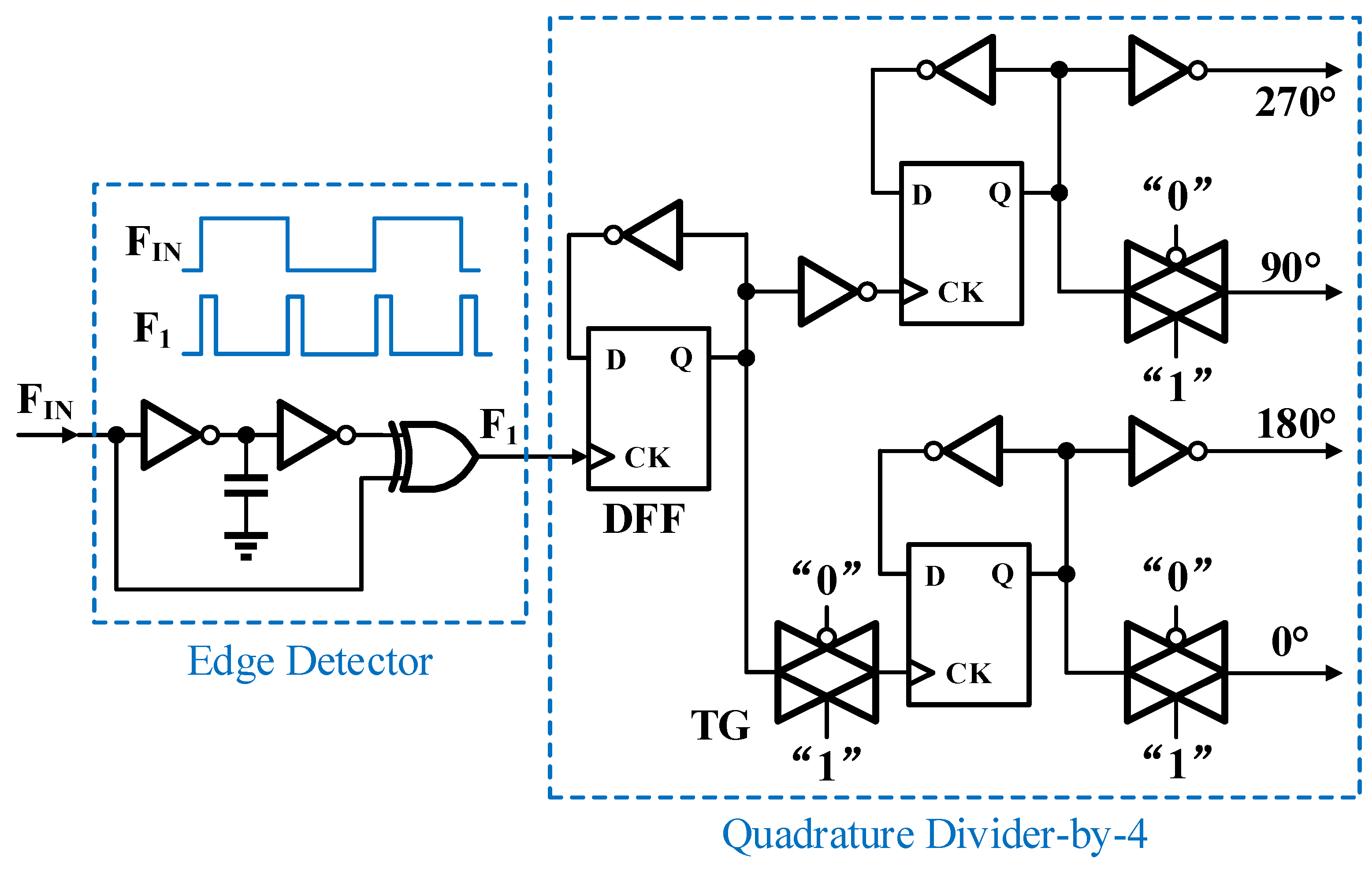
Figure 3.
Proposed square-to-triangular converter.
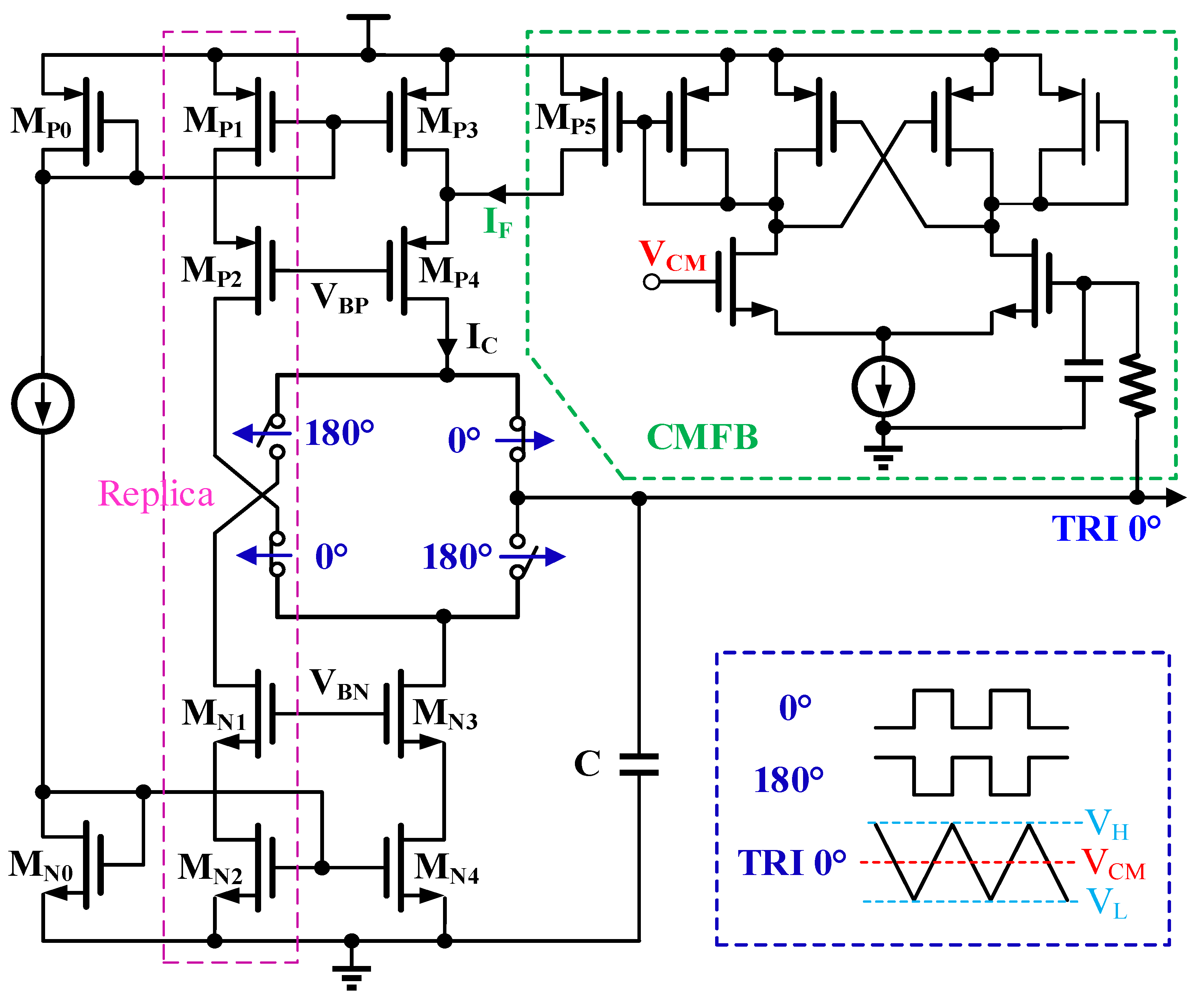
Figure 4.
Proposed circuit topology of phase interpolators.
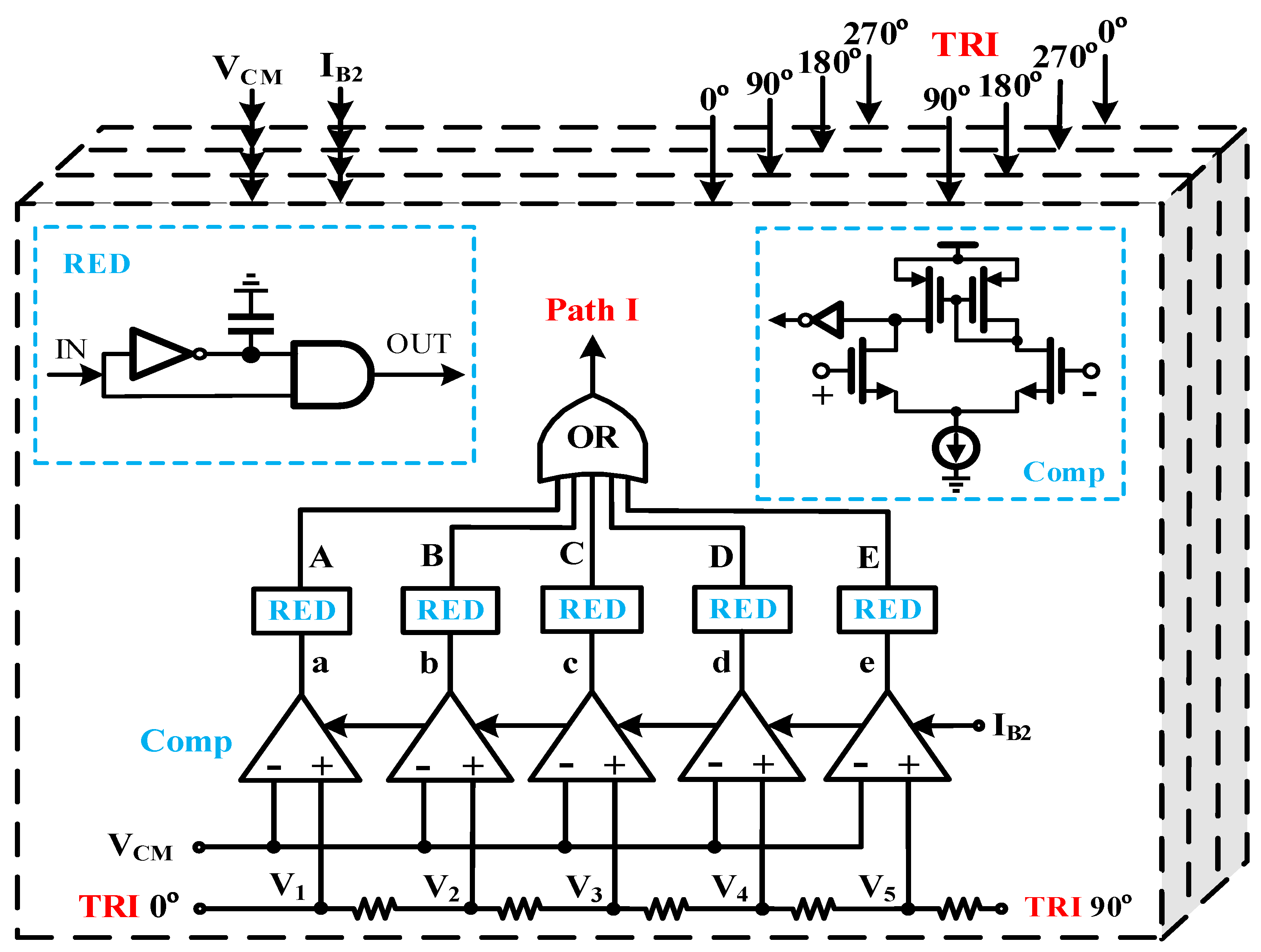
Figure 5.
Timing diagram of the proposed phase interpolator.
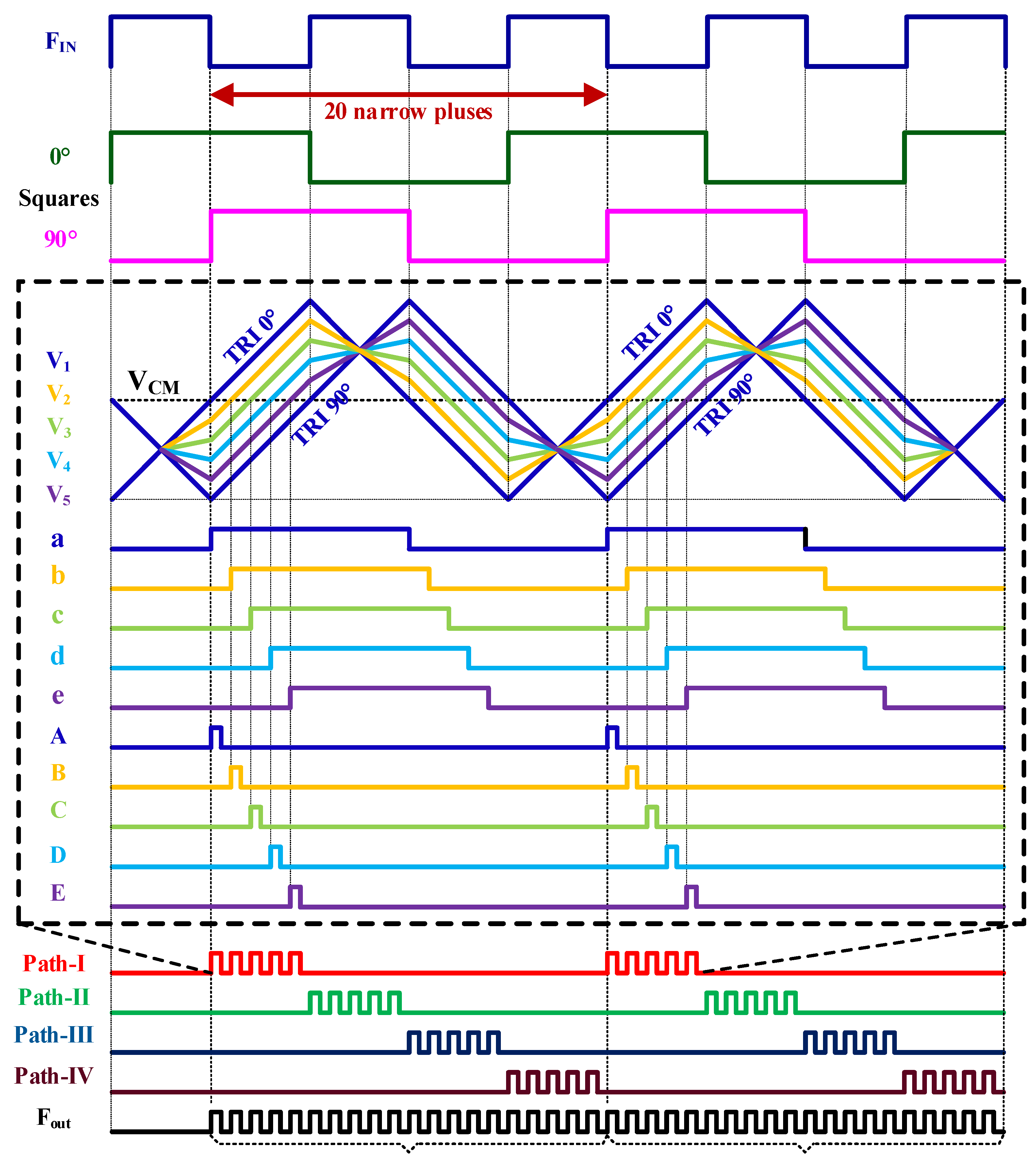
Figure 6.
Presented frequency multiplier layout in 65-nm CMOS.

Figure 7.
Transient behaviors under VDD variations.
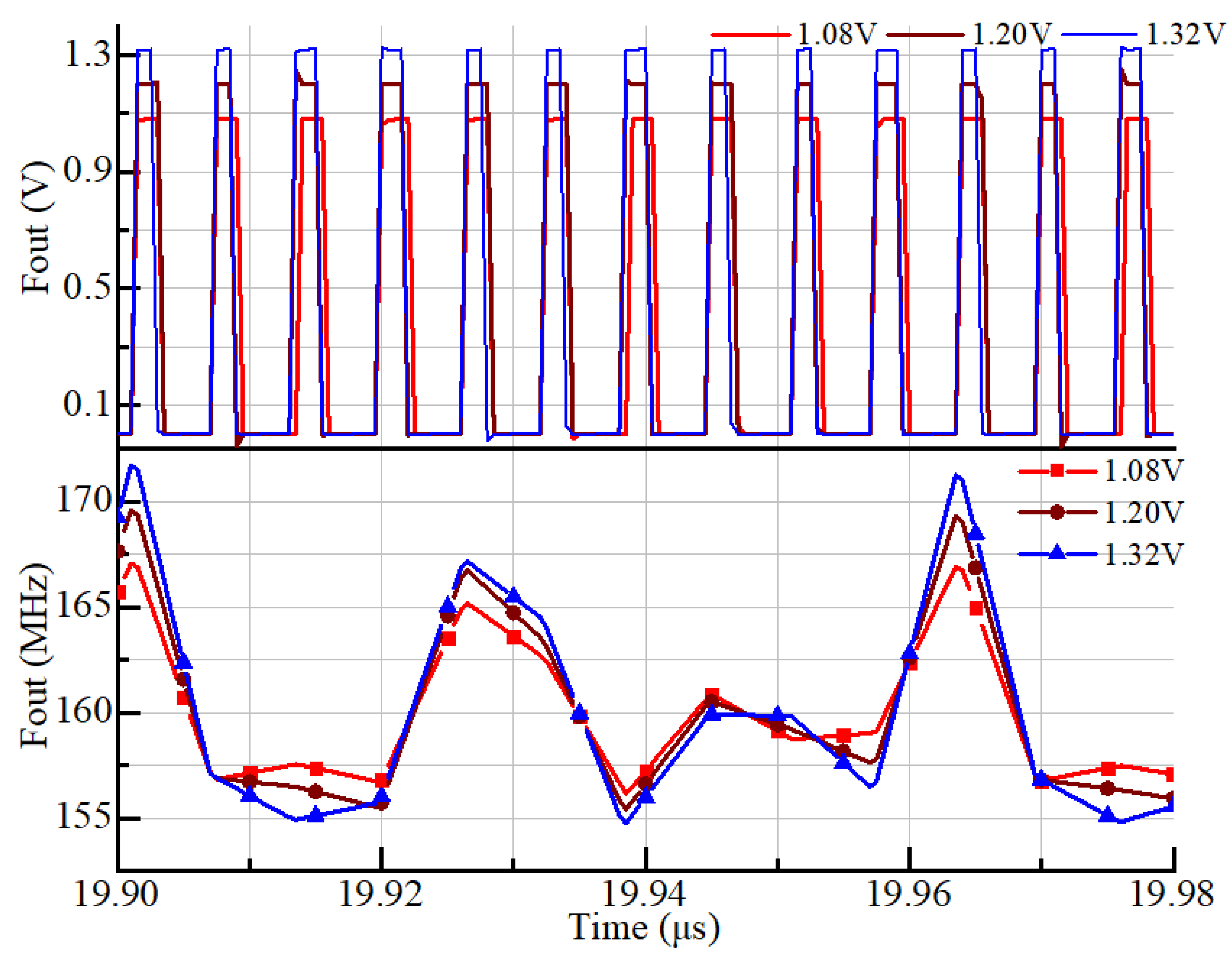
Figure 8.
Transient behavors under process and temperature variations.
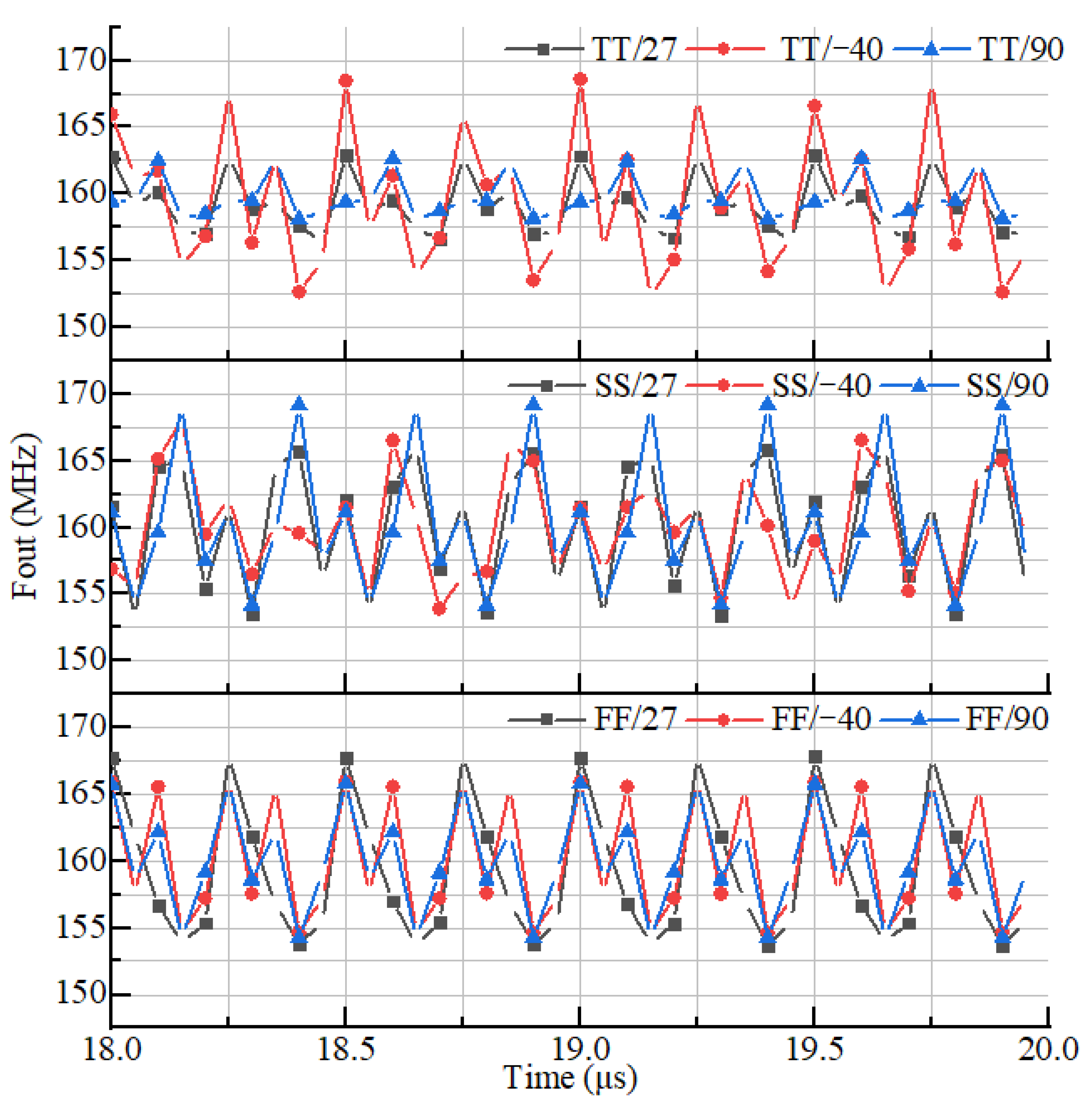
Figure 9.
Output spectra under different input frequencies.
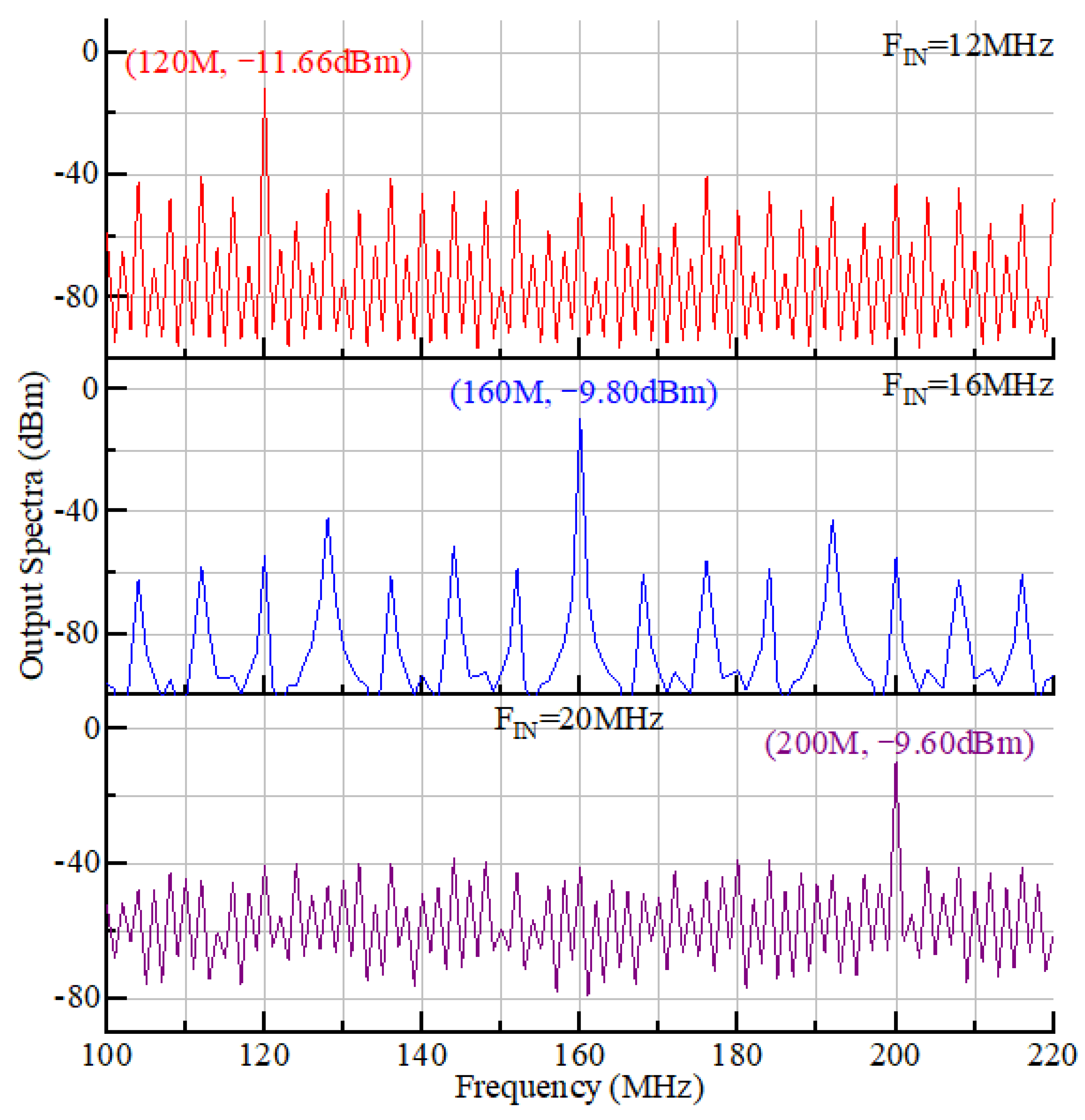

Table 1.
Performance summary and comparison.
| [3] | [12] | [13] | [14] | This work | |
| CMOS process | 65 nm | 65 nm | 40 nm | 40 nm | 65 nm |
| Architecture | MR-ILFM | EPCG | MDLL | CL-CPPD | TRPI |
| VDD (V) | 1.0 | 1.2 | 1.8 / 1.1 | 0.9 | 1.2 |
| FIN (MHz) | 4300-5800 | 80-600 | 19.2 | 17100 | 12-20 |
| Fout (GHz) | 22.4-40.6 | 0.32-2.4 | 0.15-0.52 | 136.8 | 0.12-0.20 |
| Mult. factor | 5 / 7 | 4 | 8-27 | 8 | 10 |
| Error correction | No | Yes | Yes | No | No |
| Pdiss (mW) | 10 | 2.85 | 2.6 | 41.4 | 0.45 |
| Area (mm2) | 0.22 | - | 0.05 | 0.37 | 0.06 |
| Efficiency (%) | 0.33 | - | - | 1.33 | 9.60 |
Disclaimer/Publisher’s Note: The statements, opinions and data contained in all publications are solely those of the individual author(s) and contributor(s) and not of MDPI and/or the editor(s). MDPI and/or the editor(s) disclaim responsibility for any injury to people or property resulting from any ideas, methods, instructions or products referred to in the content. |
© 2025 by the authors. Licensee MDPI, Basel, Switzerland. This article is an open access article distributed under the terms and conditions of the Creative Commons Attribution (CC BY) license (http://creativecommons.org/licenses/by/4.0/).
Copyright: This open access article is published under a Creative Commons CC BY 4.0 license, which permit the free download, distribution, and reuse, provided that the author and preprint are cited in any reuse.


