
Submitted:
21 February 2025
Posted:
24 February 2025
You are already at the latest version
Abstract
In Wireless Power Transfer Systems (WPTS), variations in the load connected to the receiver can cause instability in the waveforms of output voltage and current due to their sensitivity to changes in load impedance. To overcome such drawbacks, this paper presents a control scheme for regulating voltage and current at the output of a WPTS system with the Double-LCC topology. The proposed method is based on estimating secondary-side parameters while assuming a constant coupling coefficient that remains close to its intended value during operation. The methodology begins with the mathematical modeling of the primary and secondary resonant circuits. By measuring the input voltage and current, the system estimates the load impedance, which is then used to derive the expected output voltage and a reference for the input voltage. To maintain a stable output, the system dynamically adjusts the input voltage, ensuring that it aligns with the theoretical reference value. Analytical calculations and simulations were performed using the MATLAB/Simulink platform to validate the proposed approach. Simulations confirmed the theoretical predictions for a wireless system operating at 120 kHz with a power transfer of 100 W. The results demonstrated that the load voltage remains stable at 32 V, even under varying load conditions, while the output current remains at 3 A despite fluctuations in battery voltage.
Keywords:
Control
; Hybrid Double-LCC Topology
; Parameter Estimation
; Wireless Power Transfer
1. Introduction
Electric vehicles associated with micro-mobility encompass light automobiles designed for short trips, offering a sustainable, economical, and practical solution to urban transportation challenges. In such systems, wireless energy transfer emerges as an innovative, convenient, and safe technology for charging these vehicles. Beyond micro-mobility, this technology can also be applied to charging electronic devices, and even implantable medical equipment, among others [1]. Its success lies on its wire-free energy transfer process, which enhances safety and allows for reliable operation in humid and harsh environments [2].
The near-field resonant inductive coupling scheme is based on the principle of electromagnetic induction, where wireless energy transmission occurs between two magnetically coupled coils — one acting as a transmitter that generates magnetic flux and other as a receiver, where voltage or current is induced according to Ampère’s and Faraday’s laws [3]. Due to the lack of a ferromagnetic core to confine and guide the flux lines, flux dispersion is an inherent characteristic of this design. As a result, viable solutions must be implemented to achieve adequate efficiency for practical applications. To address this, compensation topologies are employed to minimize the reactive power demand on the source while enhancing power transmission capacity [4] [5].
The arrangement of compensation elements in the primary and secondary circuits of the system can vary, with classic configurations including SS (Series-Series), SP (Series-Parallel), PS (Parallel-Series), and PP (Parallel-Parallel) [REF]. Each acronym denotes the positioning of the compensation capacitor on the primary and secondary sides, respectively. While these classical topologies simplify the design, they have inherent limitations that hinder their widespread adoption. For instance, even a slight misalignment between the coupling coils can lead to impractically high current levels, compromising system performance. To overcome these challenges, hybrid topologies that mix classical configurations have gained relevance in enhancing system robustness and efficiency. In this article, the system under analysis is the Double-LCC topology, originally proposed in [6]. This topology features an LCC resonant network on both the primary and secondary sides, ensuring minimal variations in resonance frequency despite changes in the coupling coefficient or load conditions. Additionally, it offers the advantage of bidirectional power transfer, making it a compelling solution for high-performance wireless power transmission systems.
When implementing inductive power transfer for charging batteries in electric micro-mobility vehicles, it is essential to ensure a charging process that follows a constant current followed by a constant voltage phase. As described in [7][8], the battery charging cycle occurs in distinct stages. Initially, the battery is charged with a constant current while its voltage gradually increases. Once the voltage reaches its maximum threshold, the charging mode shifts to constant voltage, allowing the current to decrease significantly. The cycle is complete when the current reaches a predefined cutoff value. Analyzing these two stages through the lens of Ohm’s Law, the load resistance increases progressively throughout the charging process, meaning it is not constant. Consequently, variations in load resistance lead to fluctuations in output voltage, which must be carefully managed to ensure efficient and stable power transfer.
Significant efforts have been dedicated to output voltage control in wireless power transfer (WPT) systems with time-varying loads [9][10][11]. In most cases, the literature suggests communication between the secondary and primary circuits to achieve regulation. However, this approach increases system complexity and cost, as it typically requires a dedicated wireless communication system between both stages.
To address this challenge, implementing a control strategy that relies solely on a primary-side controller, without feedback from the secondary circuit, can be a valuable alternative. This approach reduces overall cost, complexity, and system size while enhancing performance and reliability [12]. In [9],a control method was proposed for the SP topology, applied to implantable devices. By analyzing the input impedance, mutual inductance, and load, the system could estimate the output voltage, enabling control without direct measurements on the secondary side. A similar technique was applied in [10] for the S-LCL topology. Meanwhile, in [11], the author proposed an estimation method for voltage and current in the load of a system utilizing an LCC resonant network on both primary and secondary sides. By monitoring the currents in the primary inductors and filter , along with the inverter output voltage, it was possible to assess secondary circuit behavior and execute control adjustments accordingly.
To reduce system complexity while ensuring high performance, this work proposes a method for estimating the load and output voltage in a wireless power transfer system for charging electric micro-mobility vehicles. The approach utilizes a Double-LCC hybrid compensation topology, relying on a stable and well-defined coupling factor. In this proposal, the usage of concentric solenoid coils is crucial in maintaining a consistent coupling coefficient, even in the presence of misalignments.
Once the coupling is established, voltage or current control at the load is achieved based on primary-side estimations. These estimations are derived from the total equivalent circuit impedance, the inverter’s output current, and its output voltage. Finally, variations in load demand or battery voltage are accounted for by dynamically adjusting the duty cycle of the single-phase full-bridge square-wave inverter. By modulating the output voltage of the DC-AC converter, the system ensures a stable and precisely regulated load voltage or current, guaranteeing the required operational conditions.
2. Project Analysis
2.1. Principles
The diagram of the proposed wireless power transfer system is depicted in Figure 1. This system consists of three fundamental sections: the single-phase square-wave DC-AC converter, the resonant network, and the load, constituting a double-LCC topology. The power switches, S1-S4, are MOSFETs that compose the inverter. and represent the self-inductances, while and denote the intrinsic resistances of the transmitting and receiving coil windings, respectively. The mutual inductance between the coils is represented by M. The resonant circuit is then formed by adding and , which act as the compensation capacitors. and represent the filter capacitances, while and correspond to the filter inductance. and represent the resistances of the filter inductances. The indices ’1’ and ’2’ denote components in the primary and secondary sections, respectively. The DC input voltage source is denoted as , while represents the square-wave AC output voltage of the inverter. The system load, which may be a resistive load or a battery, is connected to the secondary terminals with a voltage denoted as .
To help in the analytical development of the system, the T-equivalent model can be used to represent the schematic of Figure 1 [6], as shown in Figure 2.In this representation, the components of the receiving side are reflected onto the transmitting side, and are denoted by an apostrophe “ ´ “. The parameter n is defined as the turn ratio between and , as given by Equation (1). The T-model simplification represents the magnetizing inductance Lm referred to the primary side, with k as the coupling factor. Additionally, and denote the leakage inductances associated with the coils and , respectively. In this representation, a resistive load R with voltage is considered. The formulation for the corresponding variables are expressed in Equations (2)-(8) [6].
To parameterize the equivalent input impedance of the circuit in Figure 2, an analytical simplification of each branch is performed based on Thévenin’s theorem. Consequently, the equivalent impedances are defined by Equations (9)-(15). For clarity, the analyzed branches are indicated in Figure 2. By considering the contribution of each branch in the equivalent model, the total theoretical impedance of the system can be determined. Through the algebraic manipulations described in Equations (16) and (17), the resulting expression is given by Equation (18).
2.2. Coupling Coil Design
Initially, the fundamental design parameters for sizing the coupling coils must be defined. These include the design frequency (), in Hertz, the peak current in the coil (), in Amperes, the desired inductance value (), in Henries, and the internal radius (), in meters. The copper resistivity is and the magnetic permeability (), corresponds to .
Next, the cross-sectional area of the AWG conductor wire is calculated, along with the number of conductors in parallel. In alternating current applications at high frequencies, the skin effect significantly increases the resistance of the conductors. As a result, Joule heating losses rise, and the effective cross-sectional area of the cable decreases. To mitigate these undesirable effects, multiple twisted cables, known as Litz wires, are used to form the coupling coil conductor. Therefore, the cable cross-sectional area, in , must be determined according to Equation (19). Based on Equation (19), the Litz conductor should be composed of several wires, each with a cross-sectional area equal to or less than .
After selecting the AWG wire for the project, its values for the diameter with insulation of the chosen conductor , in meters, and the wires current-carrying capacity , in Amperes, must be used. The minimum number of conductors in parallel that satisfies the design requirements can then be calculated using Equation (20), yielding the smallest integer value greater than or equal to (minimum number of conductors).
The calculation of the inductance of the coupling coils primarily depends on the chosen geometry. For both the primary and secondary coils, a solenoid configuration is selected, where a conductive wire is wound in a spiral, forming a cylindrical shape. This choice is made because solenoid coils exhibit minimal variation in the coupling factor, even when there are misalignments. Given the defined geometry, the inductance value is calculated, in Henries, using Equation (21). Here, represents the relative permeability of the solenoid core material, which, in this case, is the air and it is approximately equal to 1. N denotes the number of solenoid turns. A indicates the cross-sectional area of the solenoid based on the previously defined internal radius , in square meters, and is the length of the solenoid, in meters.
To determine the total length of the solenoid , the number of turns N must be multiplied by the total diameter of the litz wire . Additionally, 30% should be added to the calculated length to account for non-idealities in practical implementation. Equation (22) is then derived. Additionally, the approximate total length of the conductor can be calculated by multiplying the number of turns of the coil by the length of a single circumference, which is equal to , as shown in Equation (23).
The total diameter of the set of conductors in parallel can be determined using Equation (24), where represents the total area of the conductor set in parallel, calculated according to Equation (25).
Given that the process of modeling and constructing the coils involves several interdependent steps, a pseudo-code is provided in Algorithm 1 to help clarify the presented methodology.
| Algorithm 1:Pseudo-algorithm for physical coil design. |
|
The values obtained for the dimensioning of the primary and secondary coils are summarized in Table (Table 1).
2.3. Load Estimation
The input impedance of the system can be determined by measuring the voltage and the current , with their respective amplitudes represented by and . The impedance is related to the phase angle between and . Therefore, the magnitude and phase angle of the input impedance can be defined as shown in Equation (26).
The real and imaginary components can be expressed as shown in Equation (27).
Using Equations (18) and (27), the equivalent input impedance can ultimately be rewritten as given in Equation (28).
Equation (28) is algebraically manipulated to isolate the variable R. This allows for the calculation of the estimated load resistance of the system, denoted as , as given in Equation (29).
For simplification purposes, it is considered
The parameters in Equation (29) are calculated using Equations (9)-(15). It can be observed that the load estimate can be derived from the system’s input impedance, which is solely dependent on parameters obtained from the primary circuit. For this purpose, the characteristic parameters of the wireless power transfer system — namely, , , , , , , , , , , , , , and k — are constants and are known.
The system’s output voltage, characteristic of the load, can be projected based on a defined coupling factor. It is important to note that k must remain constant or very close to the design value, thus excluding conditions where . To achieve this, the estimated load resistance is used to determine the equivalent output voltage.
2.4. Output Voltage Control
A single-phase full-bridge inverter is used to power the circuit. The relationship between the DC input voltage, , and the magnitude of the high-frequency AC output voltage of the inverter, , can be expressed as shown in Equation (35) [13].
In wireless power transfer systems, the goal is to charge the load in a manner that ensures a constant voltage or current, providing optimal performance and protecting the load from undesirable voltage fluctuations [8]. However, due to frequent load variations during charging, the output voltage and current may become unstable. To simplify system design, a control scheme is proposed that maintains a stable and appropriate load voltage or current, based on the estimation of the secondary circuit parameters. For this, the primary-side data, and , are utilized.
To keep or the current stable, the evaluation is based on the inverse analysis of the equations presented in (30)-(33). By setting a predetermined and required value for , and knowing the estimated load , the output current can be determined.
From the development of the equations, is calculated, and consequently, the required output voltage of the reference inverter, , is determined. After comparing with , the error e is sent to a PI controller. The controller then adjusts the duty cycle of the inverter PWM, modifying and ensuring that remains constant at the proposed design value.
3. Simulation Results and Discussion
3.1. Voltage Source Operation
3.1.1. Load Step-Up
The schematic of the proposed control strategy is illustrated in Figure 3(a), while Figure 3(b) presents the details of the applied PI controller. For the simulation analyses, MATLAB®, in combination with Simulink®, was utilized to validate the secondary data estimation and plant control. The design parameters defining the double-LCC hybrid topology used in the system simulation are listed in Table 2. As stated in [6], the transferred power P can be determined using equation (36).
With an input DC voltage of 36 V, the amplitude of the output voltage of the single-phase inverter is 45.8 Vpeak, as given by equation (35). By substituting the variables in equation (36) with the corresponding values from Table 2, the designed secondary output voltage is determined to be 32.4 Vrms. Consequently, given the power and voltage, the coupled design load resistance R must be 10,505 .
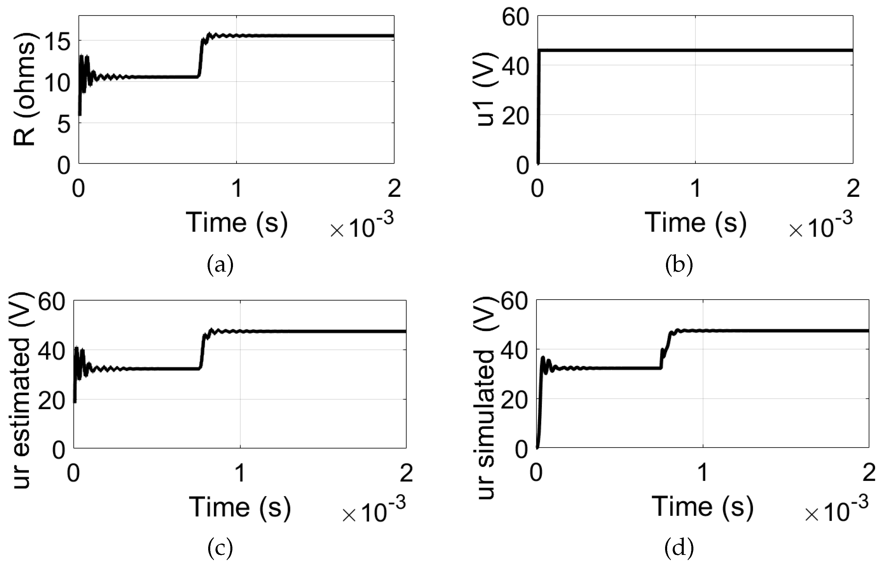
As the load increases, the resistance rises accordingly. In this simulation scenario, an increment of 5 is considered, resulting in a total resistance of 15.505 . The figures depicting the simulation results for the system under a load step-up condition, in open-loop, are shown in Figure 4. For , it is observed that the load resistance can be accurately determined using the estimation given by equation (29), as shown in Figure 4(a). Figure 4(b) illustrates the inverter output voltage, which remains constant at 45.8 Vpeak. According to Figure 4(c) and Figure 4(d), the estimated and simulated load voltages are presented, respectively. With the load step increase, the voltage rises from 32.2 Vrms to 47.3 Vrms. It is evident that the estimated voltage closely matches the simulated value. Consequently, implementing a control method to maintain a constant voltage becomes essential.
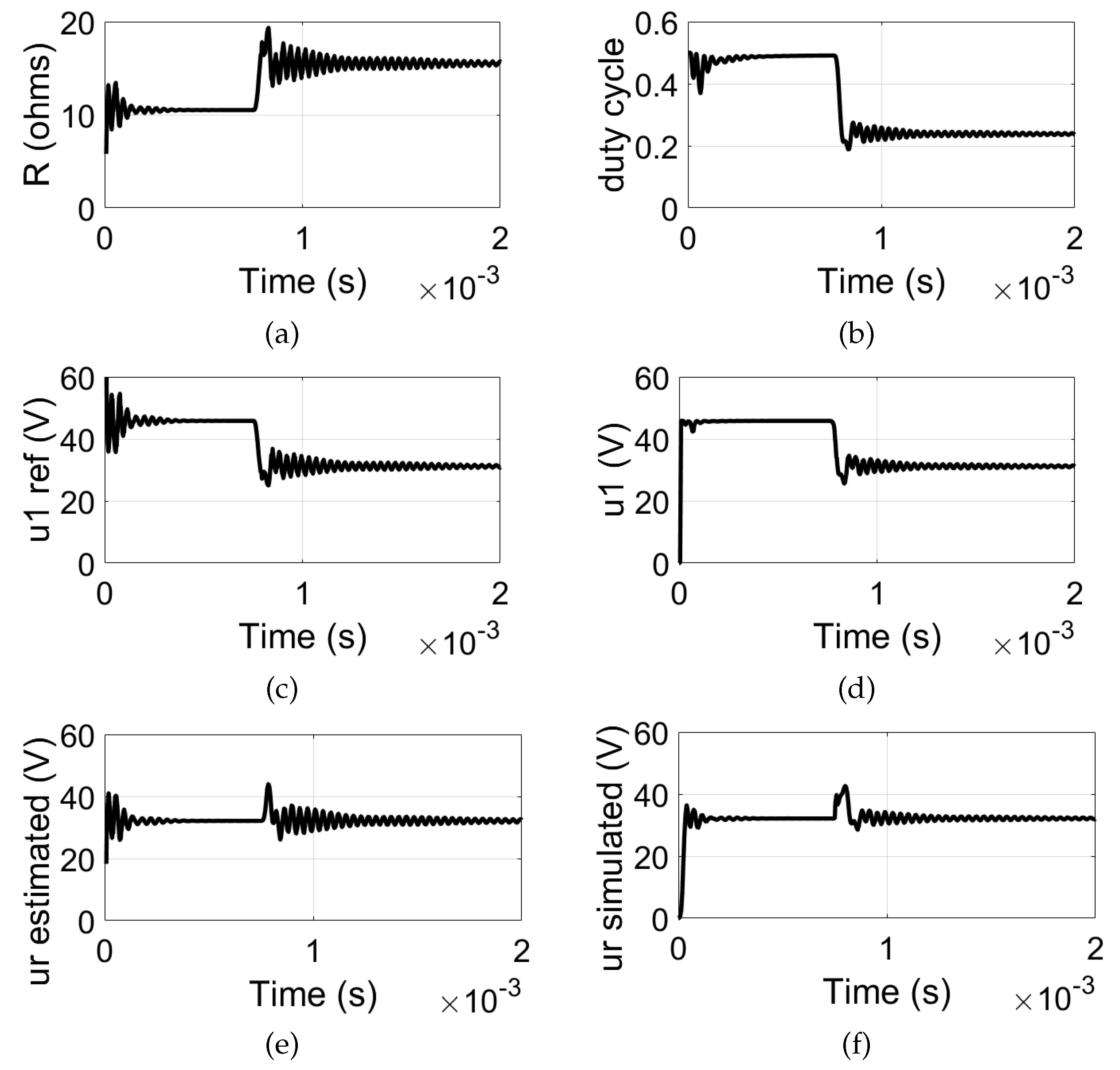
After applying the proposed control method, it is also possible to evaluate, as shown in Figure 5, the behavior of the secondary parameter estimates for a load step up from 10.505 to 15.505 . In Figure 5(a), it is shown the estimated load resistance. Figure 5(b) illustrates the modulating signal with the insertion of the PI controller, which reduces the modulation index from 0.50 to 0.23. As a result, the inverter output voltage adjusts accordingly to maintain a constant load voltage at the load.
According to Figure 5(c) and Figure 5(d), the calculated reference inverter output voltage and the simulated input voltage are presented. Before the variation in R, remains at 45.8 Vpeak. After the change, adjusts to approximately 31.5 Vpeak.
The calculation of is essential for adjusting the inverter output voltage to ensure proper control of the output voltage. The equivalence between and is then demonstrated. The difference between these values represents the error fed into the PI controller, which operates with and . Thus, in Figure 5(e) and Figure 5(f), it is shown the estimated and simulated output voltage, respectively. The output voltage remains constant at approximately 32.2 Vrms, even after the load variation. It should be noted that the maximum voltage is constrained by the modulation index limit of 0.50. Consequently, load variations are accommodated within a restricted range. Whether increasing or decreasing, these variations must occur above the nominal load design value of 10.5050 .
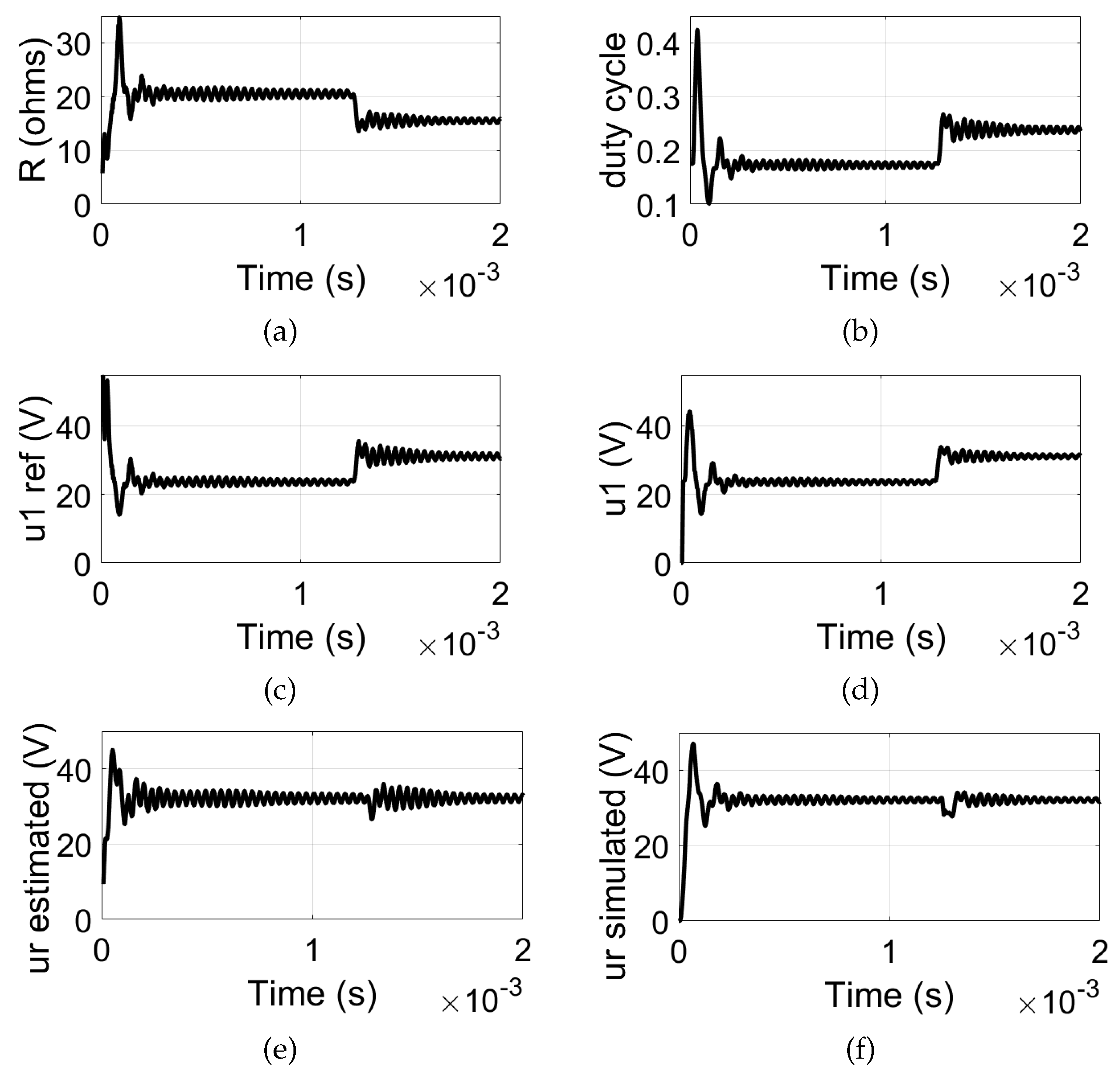
3.1.2. Load Step-Down
To evaluate the behavior of the system under a decreasing load, an initial load of 20.5050 is assumed, with a variation of 5 , resulting in a final load of 15.5050 . The simulation results obtained are shown in Figure 6.
In Figure 6(a), the load resistance is accurately estimated. In Figure 6(b), the modulation index increases from approximately 0.175 to 0.235. As shown in Figure 6(c) and Figure 6(d), the reference voltage and the simulation voltage converge to initial values of 24.2 Vpeak and final values of 30.1 Vpeak.
Thus, by readjusting the inverter output voltage, the output voltage can be observed to remain constant at the predefined value. According to Figure 6(e) and Figure 6(f), the estimated and simulated output voltages are presented, clearly demonstrating that stays constant and close to the defined value despite the load step-down.
3.2. Current Source Operation
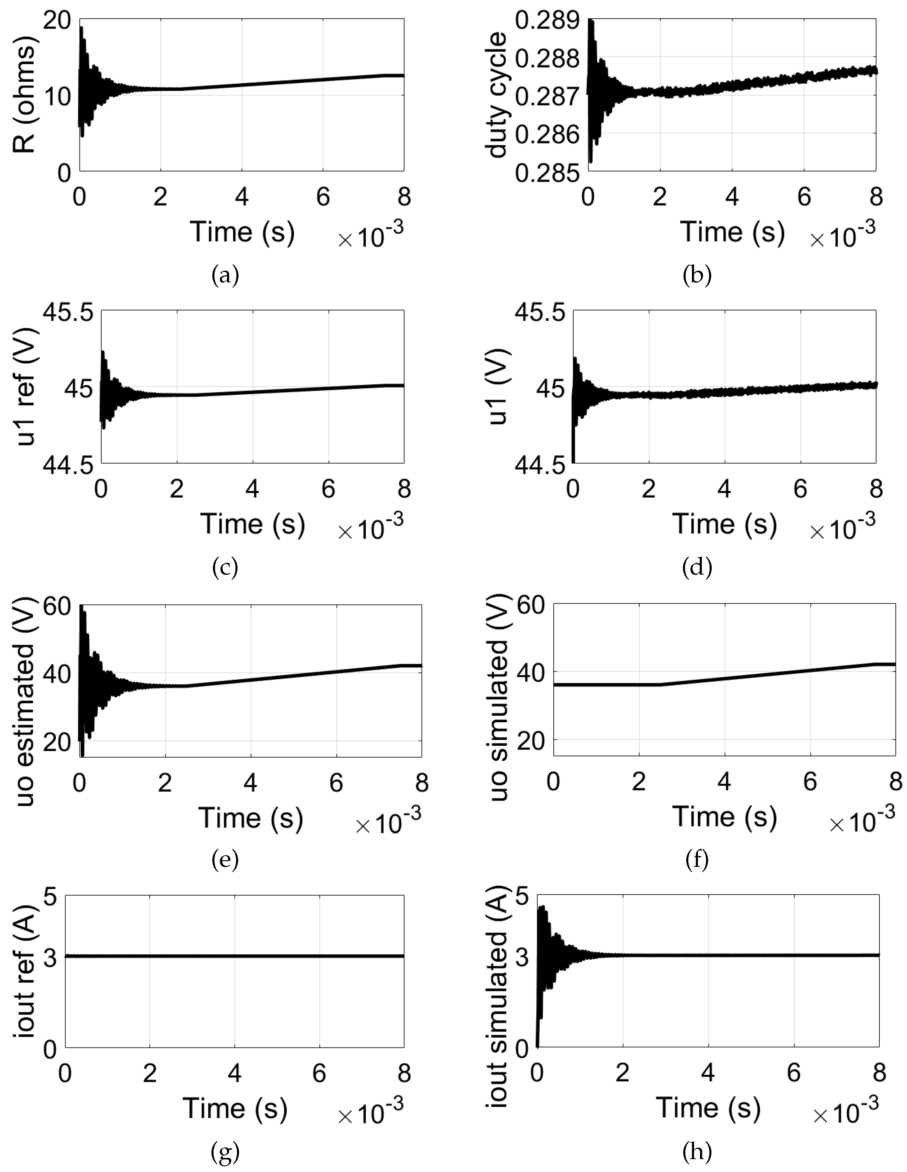
Moving on to practical applications, it is possible to propose battery charging using inductive wireless power transfer with the double-LCC topology, as shown in Figure 7. An important characteristic of the hybrid topology under analysis is that the LCC resonant network on the secondary side functions as a current source, which is ideal for the charging process with constant current (an important feature of the actual battery charging systems). Given this, it is necessary to incorporate a rectifier circuit for coupling with the battery, as it provides a DC voltage that varies over the course of the charging time.
To simulate a battery charging process with increasing voltage, the load with varying voltage was modeled. Initially, is set to 36 V and gradually increases to 42 V. Unlike the previous analysis, which focused on maintaining a constant voltage, the objective now is to supply the load with a fixed current of 3 Arms. Using equations (30)-(33), the reference voltage that ensures a constant load current at the required value can be determined. is then compared to the actual voltage , and the difference corresponds to the error e, which is fed to the PI controller. The controller adjusts the switching signal of switches , thereby regulating the inverter output voltage and ensuring a constant output current.
The simulation results are presented in Figure 8. Figure 8(a) shows the curve of the estimated load resistance, which exhibits an increasing trend from 10.7 to 12.5 . However, exhibits an error of approximately 1.5 during the steady-state, which does not significantly impact the control performance. In Figure 8(b), the modulation index for controlling the switches shows a minimal increase, but it is sufficient to adjust the voltage . As shown in Figure 8(c) and Figure 8(d), both and exhibit equivalent and ascending behavior.
The battery voltage is satisfactorily estimated when compared to the simulation value, as shown in Figure 8(e) and Figure 8(f). Figure 8(g) and Figure 8(h) illustrate the reference and simulation output current, respectively. The simulated current converges to the required value of 3 Arms. Finally, the constant value of the current is maintained, even after variations in the battery voltage during charging, thereby validating the proposed control strategy.
4. Conclusions
This paper proposes a control scheme for regulating the output voltage or current of a wireless power transfer system used for recharging the batteries of electric vehicles associated with micromobility. The analytical modeling of the parameters on the receiver side was carried out based on the measurement of the primary voltage and current, as well as the calculation of the total equivalent impedance observed by the source.
The double-LCC hybrid topology, operating at a switching frequency of 120 kHz and designed to transmit 100 W, was used. The desired output voltage is 32.4 V, with a load resistance of 10.5050 . The load resistance of the system was successfully estimated, accounting for both increasing and decreasing variations, while maintaining a coupling coefficient close to the design value.
Furthermore, it was possible to emulate a coupled battery with varying voltage during charging. In the proposed simulations, the charging steps were correctly evaluated. With the load resistance and the desired output voltage, the reference inverter output voltage was calculated to ensure that remained stable and constant, even after load variations. Similarly, the charging current was controlled at the desired value by calculating and maintaining the reference voltage accordingly.
The difference between the reference inverter output voltage and the simulation voltage was fed to the PI controller, which adjusted the modulation index of the switches in the single-phase inverter. As a result, was readjusted, ensuring a constant and fixed output voltage or current. The simulation results ultimately validated the proposed analytical formulations, using MATLAB/Simulink® software. For future projects, we aim to obtain experimental results of the control scheme through the implementation of the analyzed wireless power transfer strategy.
Author Contributions
Conceptualization and methodology, R.B.G. and T.M.T.; validation, T.M.T. and R.d.S.S.; formal analysis, R.B.G. and T.M.T.; investigation, T.M.T, R.d.S.S. and W.S.d.S; resources, T.M.T., R.d.S.S., M.A.G.d.B., W.S.d.S., and R.B.G.; writing—original draft preparation, T.M.T. and R.B.G.; writing—review and editing, T.M.T, M.A.G.d.B. and R.d.S.S.; supervision, R.B.G.; project administration, R.B.G. and W.S.d.S.; funding acquisition, R.B.G. All authors have read and agreed to the published version of the manuscript.
Funding
This study was financed by Federal University of Mato Grosso do Sul (UFMS) and Tutorial Education Program FNDE/MEC/PET.
Institutional Review Board Statement
Not applicable.
Informed Consent Statement
Not applicable.
Data Availability Statement
Not applicable.
Acknowledgments
The authors express their sincere gratitude to the Federal University of Mato Grosso do Sul (UFMS) and the Brazilian Ministry of Education (MEC) for their financial support and institutional backing, which were instrumental in the development of this research. Their contributions have significantly facilitated the execution of this study, providing essential resources and an academic environment conducive to scientific advancement.
Conflicts of Interest
The authors declare no conflicts of interest.
References
- Agarwal, K.; Jegadeesan, R.; Guo, Y.X.; Thakor, N.V. Wireless Power Transfer Strategies for Implantable Bioelectronics. IEEE Reviews in Biomedical Engineering 2017, 10, 136–161. [Google Scholar] [CrossRef] [PubMed]
- Liu, F.; Yang, Y.; Jiang, D.; Ruan, X.; Chen, X. Modeling and Optimization of Magnetically Coupled Resonant Wireless Power Transfer System With Varying Spatial Scales. IEEE Transactions on Power Electronics 2017, 32, 3240–3250. [Google Scholar] [CrossRef]
- Covic, G.A.; Boys, J.T. Inductive Power Transfer. Proceedings of the IEEE 2013, 101, 1276–1289. [Google Scholar] [CrossRef]
- Wang, C.S.; Covic, G.; Stielau, O. Power transfer capability and bifurcation phenomena of loosely coupled inductive power transfer systems. IEEE Transactions on Industrial Electronics 2004, 51, 148–157. [Google Scholar] [CrossRef]
- Carneiro, F.T.; Barbi, I. Análise, projeto e implementação de um conversor com transferência de energia sem fio para carregadores de baterias de veículos elétricos. Revista Eletrônica de Potência-SOBRAEP 2021, 26, 260–267. [Google Scholar] [CrossRef]
- Li, S.; Li, W.; Deng, J.; Nguyen, T.D.; Mi, C.C. A Double-Sided LCC Compensation Network and Its Tuning Method for Wireless Power Transfer. IEEE Transactions on Vehicular Technology 2015, 64, 2261–2273. [Google Scholar] [CrossRef]
- Jank, H.; Venturini, W.A.; Koch, G.G.; Martins, M.L.; Bisogno, F.E.; Montagner, V.F.; Pinheiro, H. Controle baseado em um LQR com estabilidade robusta a incerteza parametrica aplicado a um carregador de baterias. Revista Eletrnica de Potencia-SOBRAEP 2017, 22, n4. [Google Scholar] [CrossRef]
- Vu, V.B.; Tran, D.H.; Choi, W. Implementation of the Constant Current and Constant Voltage Charge of Inductive Power Transfer Systems With the Double-Sided LCC Compensation Topology for Electric Vehicle Battery Charge Applications. IEEE Transactions on Power Electronics 2018, 33, 7398–7410. [Google Scholar] [CrossRef]
- Meng, X.; Qiu, D.; Zhang, B.; Xiao, W. Output Voltage Stabilization Control without Secondary Side Measurement for Implantable Wireless Power Transfer System. In Proceedings of the 2018 IEEE PELS Workshop on Emerging Technologies: Wireless Power Transfer (Wow); 2018; pp. 1–5. [Google Scholar] [CrossRef]
- Meng, X.; Qiu, D.; Lin, M.; Tang, S.C.; Zhang, B. Output Voltage Identification Based on Transmitting Side Information for Implantable Wireless Power Transfer System. IEEE Access 2019, 7, 2938–2946. [Google Scholar] [CrossRef]
- Barbosa, C.R.; Pereira, R.N.; de Oliveira Júnior, A.A. Estimação de Tensão e Corrente na Carga de um Sistema de Transferência Indutiva de Potência. SBPC 2018. [Google Scholar]
- Thrimawithana, D.J.; Madawala, U.K. A primary side controller for inductive power transfer systems. In Proceedings of the 2010 IEEE International Conference on Industrial Technology; 2010; pp. 661–666. [Google Scholar] [CrossRef]
- Yang, J.; Zhang, X.; Zhang, K.; Cui, X.; Jiao, C.; Yang, X. Design of LCC-S Compensation Topology and Optimization of Misalignment Tolerance for Inductive Power Transfer. IEEE Access 2020, 8, 191309–191318. [Google Scholar] [CrossRef]
Figure 1.
Wireless Power Transfer Equivalent Circuit with Double-LCC Compensation Hybrid Topology.
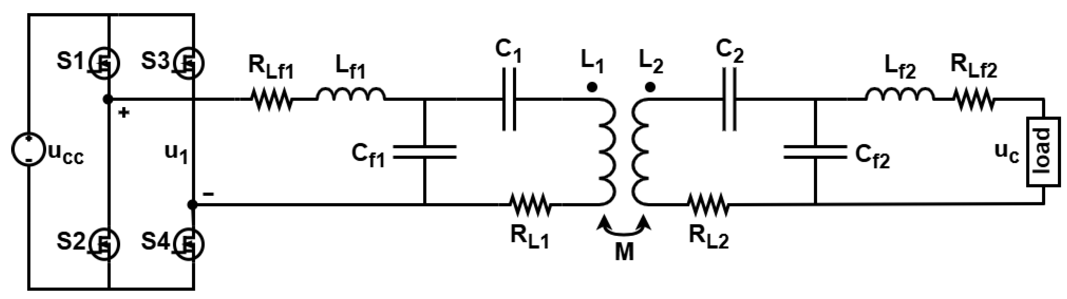
Figure 2.
T-equivalent model of double-LCC topology.
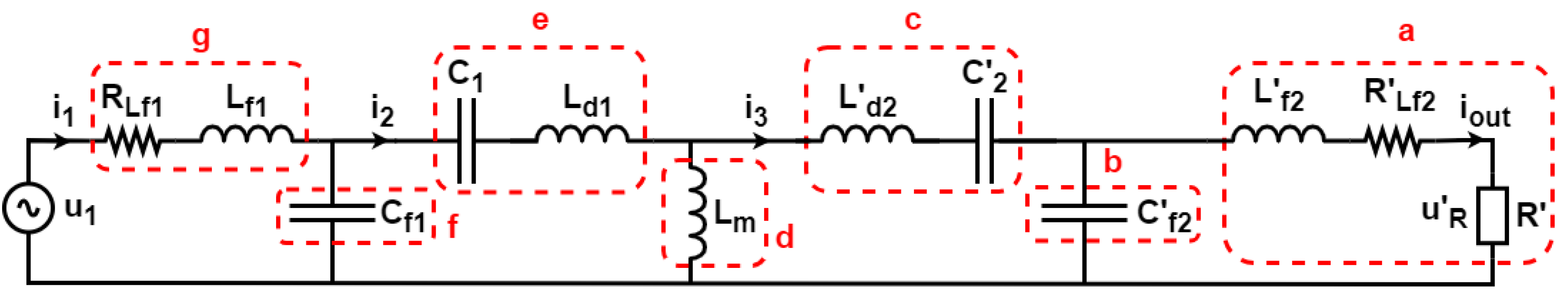
Figure 3.
(a) Proposed control strategy. (b) PI controller detail.
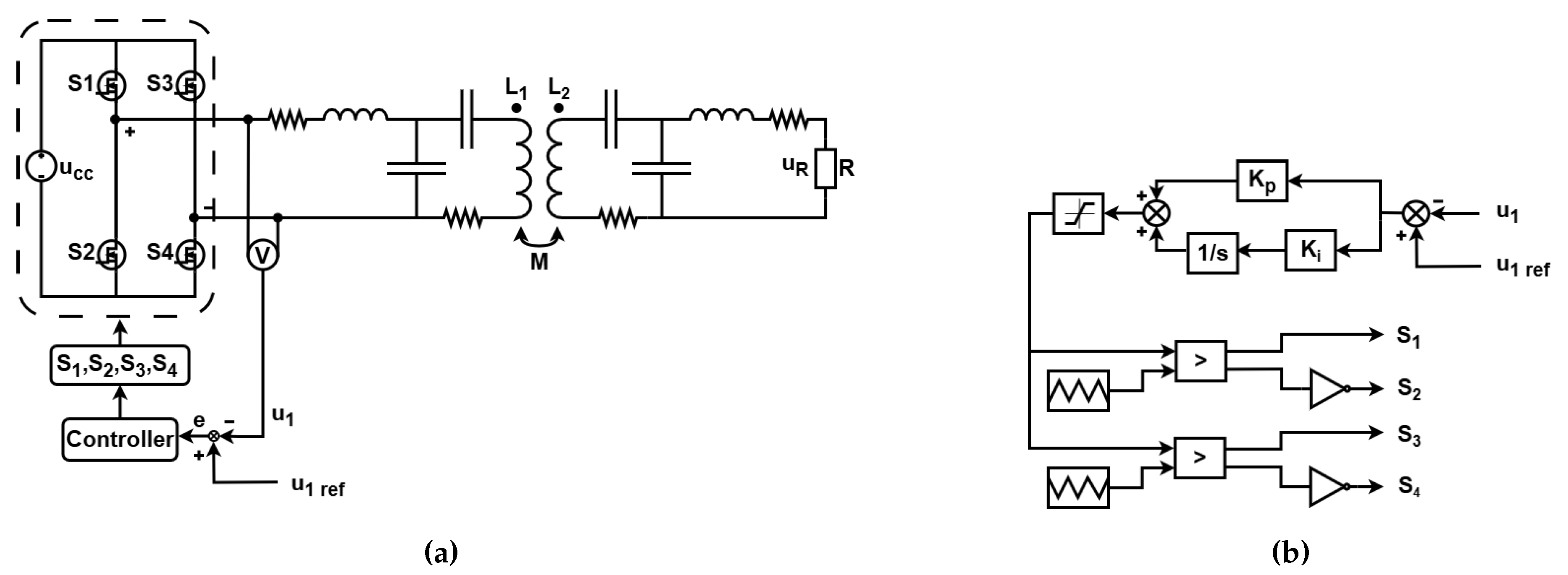
Figure 4.
Waveforms for the system without control. (a) Estimated load resistance . (b) Input voltage magnitude . (c) Estimated output voltage . (d) Simulated output voltage .
Figure 4.
Waveforms for the system without control. (a) Estimated load resistance . (b) Input voltage magnitude . (c) Estimated output voltage . (d) Simulated output voltage .
| (a) | (b) |
| (c) | (d) |
Figure 5.
Waveforms for the system with control and load step up. (a) Estimated load resistance . (b) Modulating signal for switches . (c) Reference input voltage . (d) Simulated input voltage . (e) Estimated output voltage . (f) Simulated output voltage .
Figure 5.
Waveforms for the system with control and load step up. (a) Estimated load resistance . (b) Modulating signal for switches . (c) Reference input voltage . (d) Simulated input voltage . (e) Estimated output voltage . (f) Simulated output voltage .
| (a) | (b) |
| (c) | (d) |
| (e) | (f) |
Figure 6.
Waveforms for the system with control and load step down. (a) Estimated load resistance . (b) Modulating signal for switches . (c) Reference input voltage . (d) Simulated input voltage . (e) Estimated output voltage . (f) Simulated output voltage .
Figure 6.
Waveforms for the system with control and load step down. (a) Estimated load resistance . (b) Modulating signal for switches . (c) Reference input voltage . (d) Simulated input voltage . (e) Estimated output voltage . (f) Simulated output voltage .
| (a) | (b) |
| (c) | (d) |
| (e) | (f) |
Figure 7.
Equivalent circuit with double-LCC topology and coupled battery.
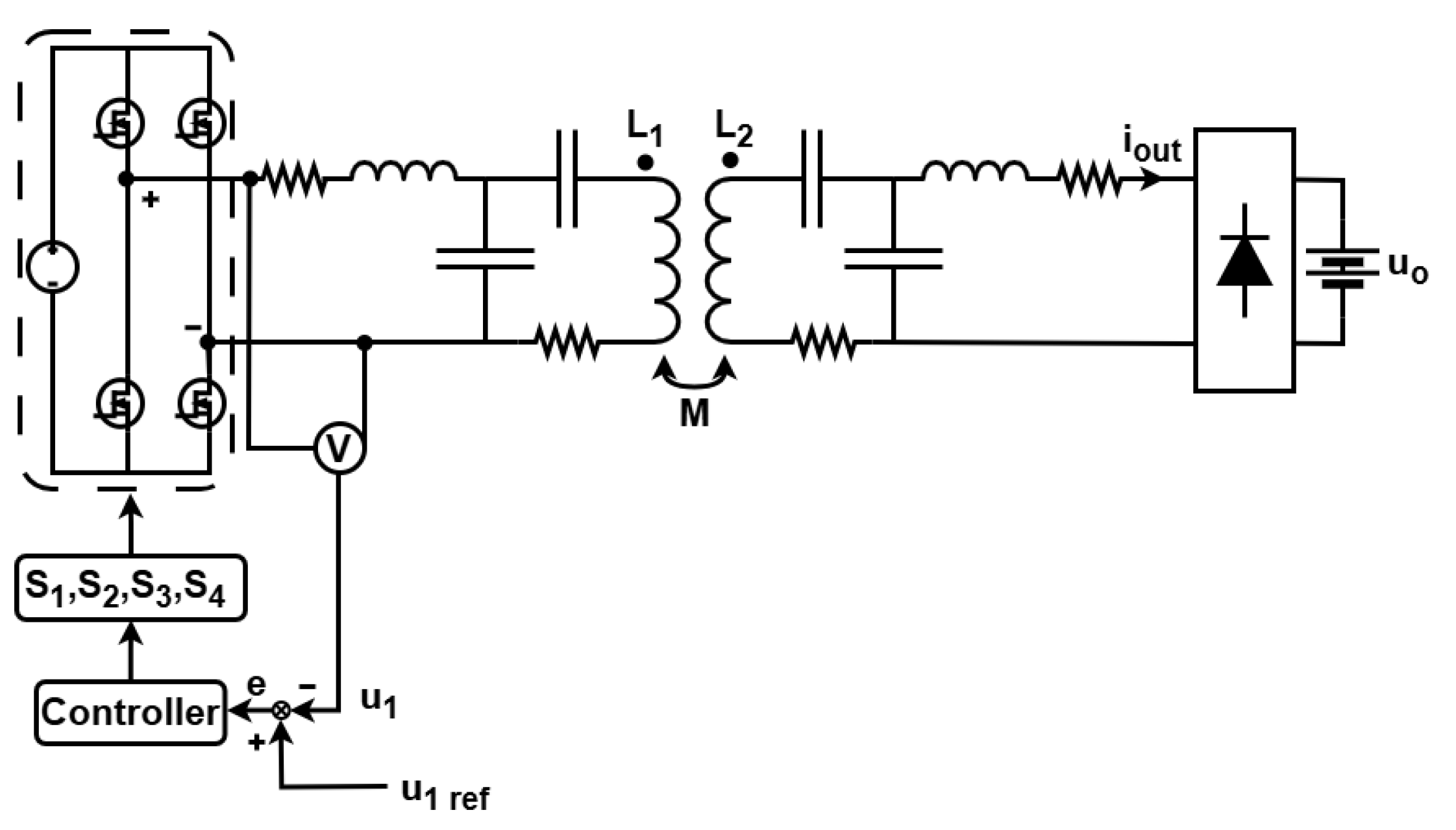
Figure 8.
Waveforms for the system with control and increasing battery voltage variation. (a) Estimated load resistance . (b) Modulating signal for switches . (c) Reference input voltage . (d) Simulated input voltage . (e) Estimated DC output voltage . (f) Simulated DC output voltage . (g) Reference ACrms output current . (h) Simulated ACrms output current .
| (a) | (b) |
| (c) | (d) |
| (e) | (f) |
| (g) | (h) |

Table 1.
Designed parameters for primary and secondary coils.
| Variable | Primary coil | Secondary coil |
|---|---|---|
| 1.72 A | 1.72 A | |
| 0.07 m | 0.10 m | |
| Conductor | [AWG 26] | [AWG 26] |
| N | 110 | 54 |
| 16 cm | 8 cm | |
| 24 m | 17 m | |
Table 2.
System parameters
| Parameter | Value |
|---|---|
| Transferred power (P) | 100 W |
| Switching frequency () | 120 kHz |
| Input voltage () | 36 V |
| Coupling factor (k) | 0.25 |
| Transmitter coil inductance () | 360 H |
| Receiver coil inductance () | 360 H |
| Filter inductance () | 35.41 H |
| Filter inductance () | 35.41 H |
| Filter capacitance () | 49.67 nF |
| Filter capacitance () | 49.67 nF |
| Primary capacitance () | 5.42 nF |
| Secondary capacitance () | 5.42 nF |
| Transmitter coil resistance () | 541.50 m |
| Receiver coil resistance () | 541.50 m |
| Filter inductance resistance () | 3.10 m |
| Filter inductance resistance () | 3.10 m |
Disclaimer/Publisher’s Note: The statements, opinions and data contained in all publications are solely those of the individual author(s) and contributor(s) and not of MDPI and/or the editor(s). MDPI and/or the editor(s) disclaim responsibility for any injury to people or property resulting from any ideas, methods, instructions or products referred to in the content. |
© 2025 by the authors. Licensee MDPI, Basel, Switzerland. This article is an open access article distributed under the terms and conditions of the Creative Commons Attribution (CC BY) license (http://creativecommons.org/licenses/by/4.0/).
Copyright: This open access article is published under a Creative Commons CC BY 4.0 license, which permit the free download, distribution, and reuse, provided that the author and preprint are cited in any reuse.


