Submitted:
18 February 2025
Posted:
19 February 2025
You are already at the latest version
Abstract
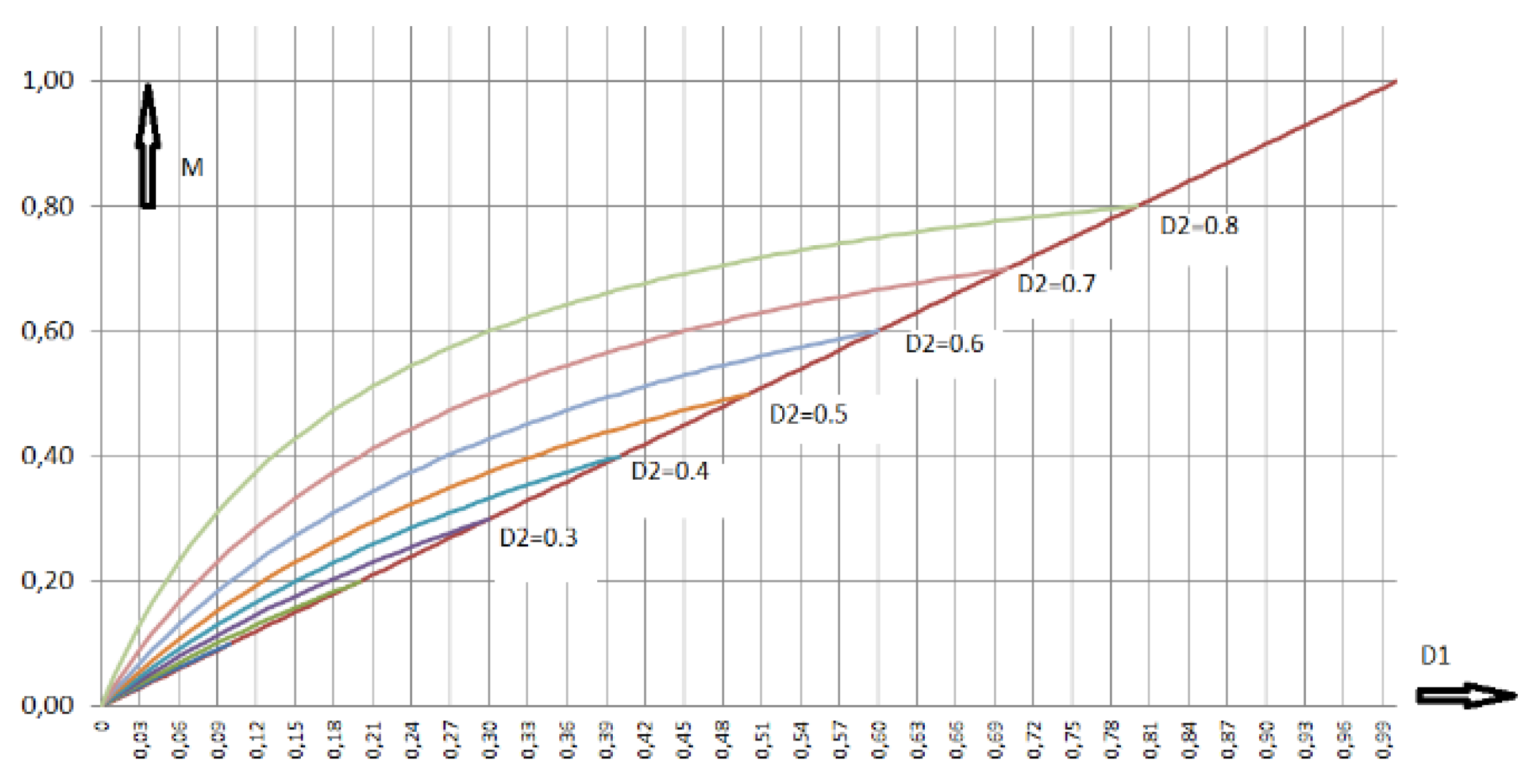
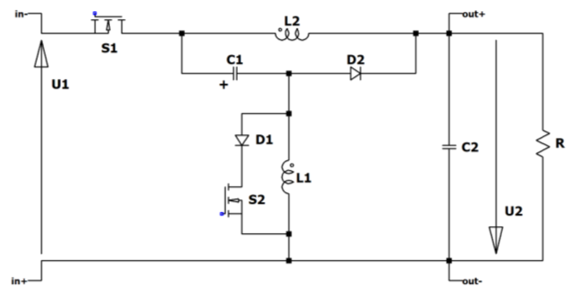
In a tristate converter the basic circuit topology is extended by an additional electronic switch and an additional diode. Three modes follow each other within one switching period. During the first mode M1 both electronic switches are on and both diodes are off. In the second mode M2 only the second switch is on and the first diode is conducting, and in mode M3 only the second diode is conducting. The voltage transformation ratio is a function of the two duty cycles of the electronic switches. In a typical tristate converter current is flowing through the second switch during the first two modes. In the converters treated here the current is flowing through the second switch only during the second mode, so the losses are reduced compared to the normal tristate converter. This is shown for the Buck, the Buck-Boost, the Boost, the Zeta, the Cuk, the Super-Boost, the quadratic Buck, and a reduced duty cycle converter. The voltage transformation ratios are depicted in diagrams. As an example the reduced loss tristate Buck is used to demonstrate the derivation of the large and the small signal models. The transfer functions are also calculated and Bode plots are shown for an operating point. The voltage and the current stress of the converters are analyzed. The considerations are proved by simulations with the help of LTSpice.
Keywords:
1. Introduction
2. Application of the Reduced Loss Tristate Concept
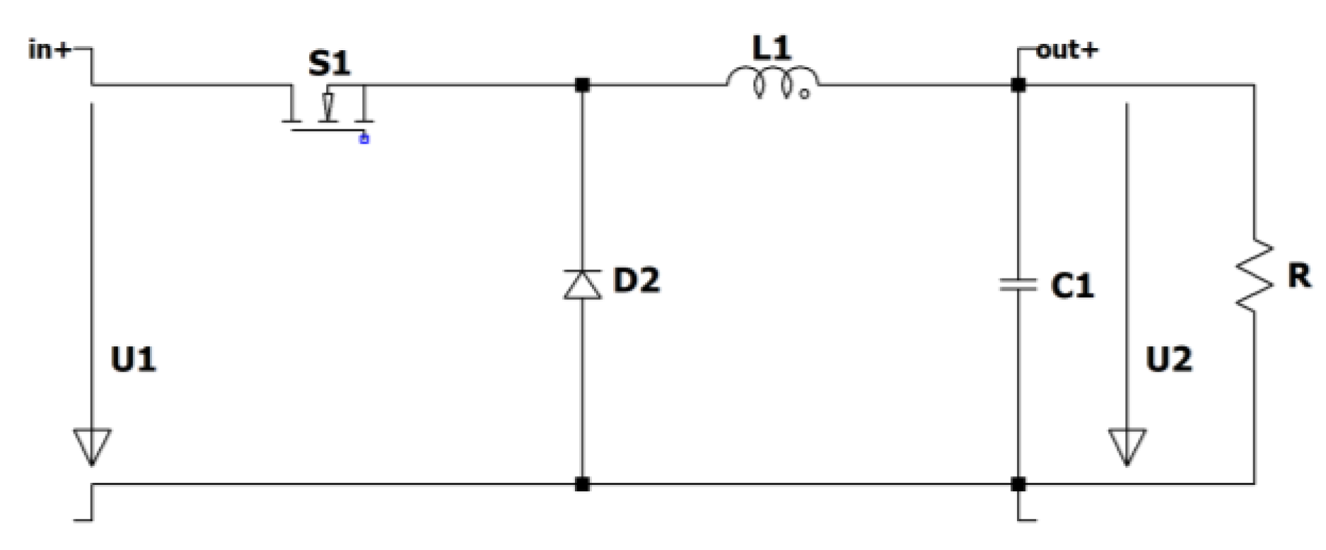
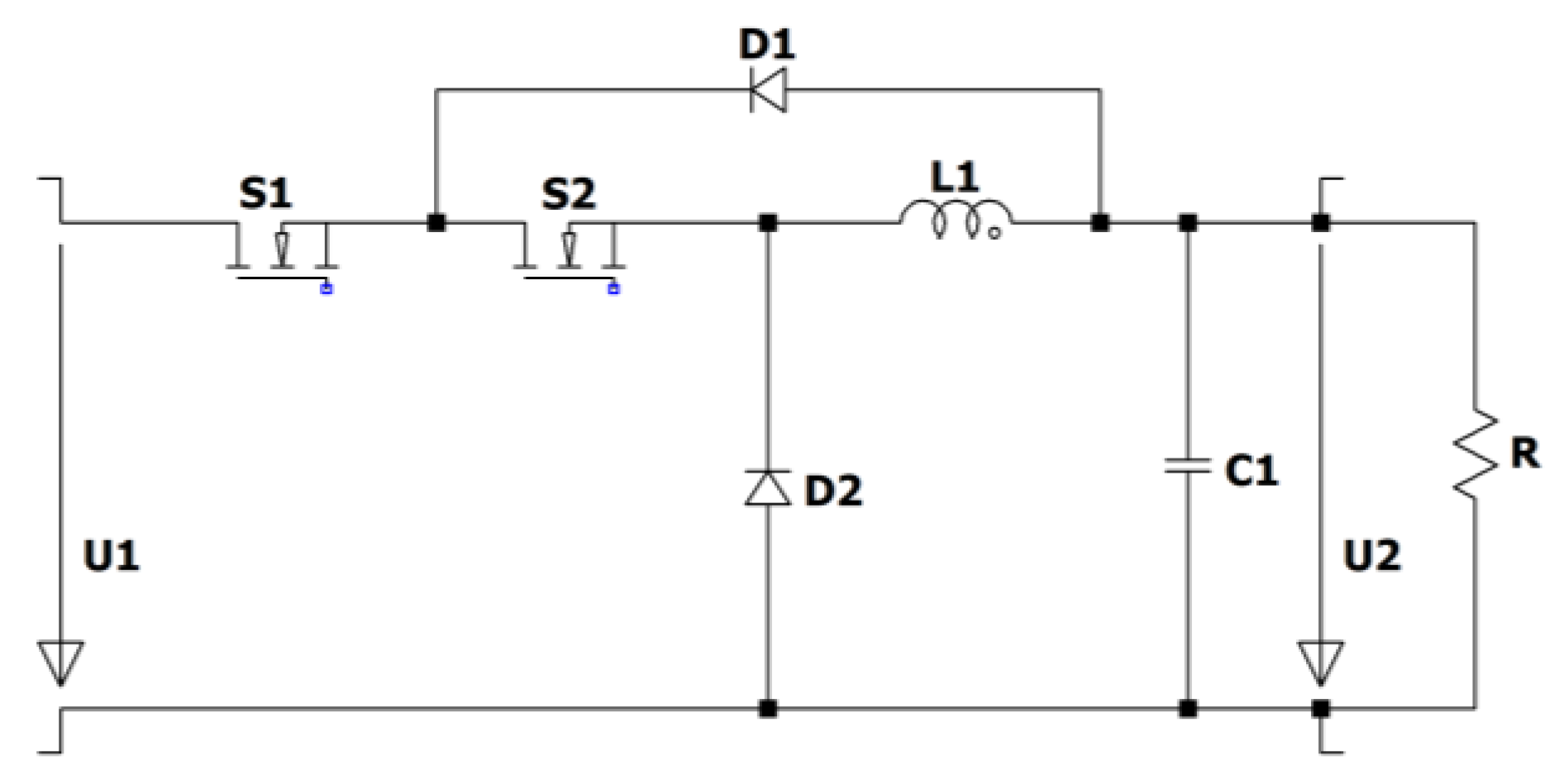
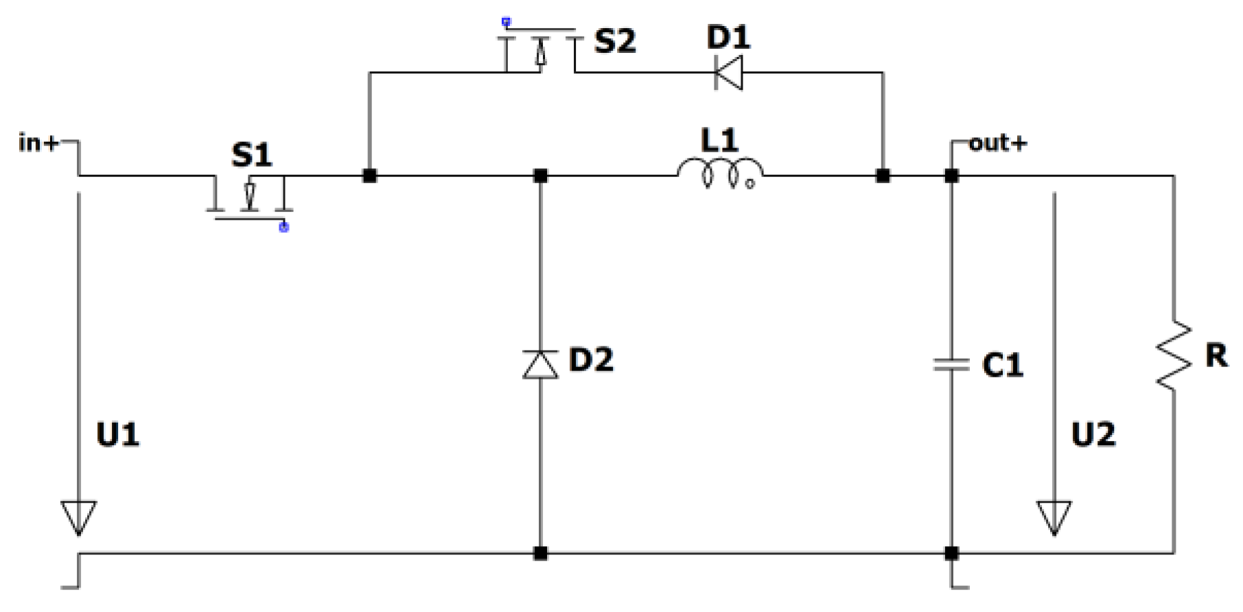
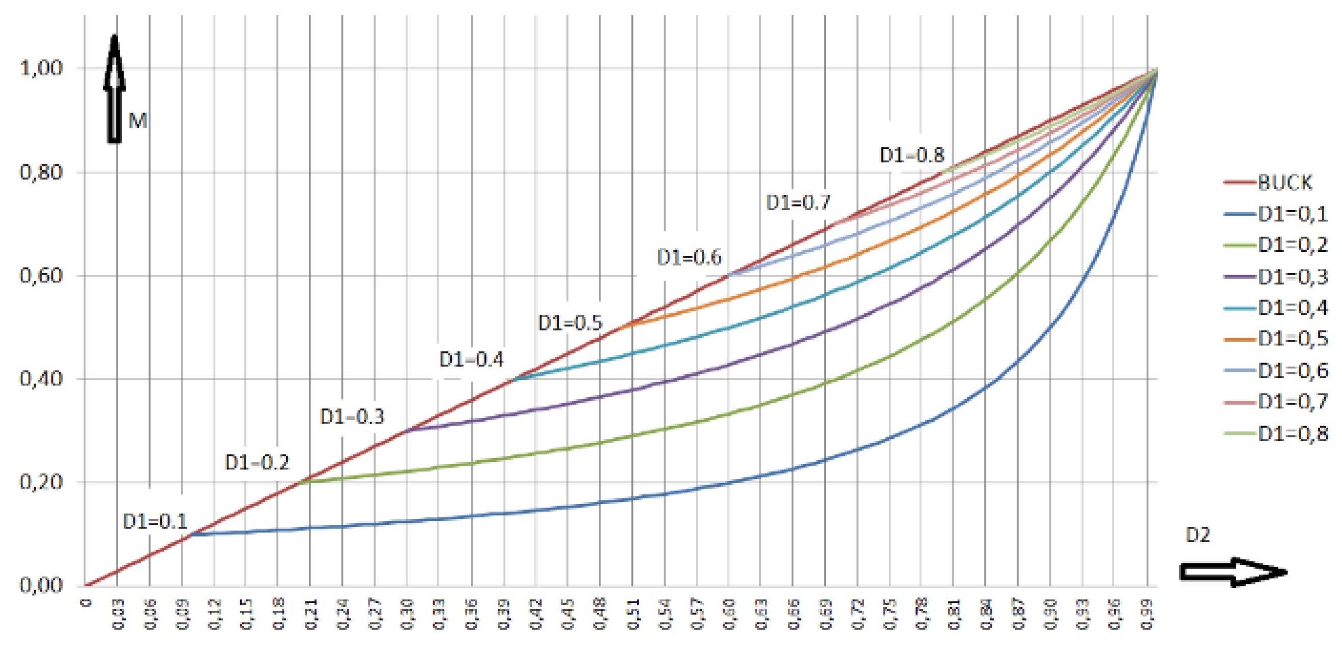
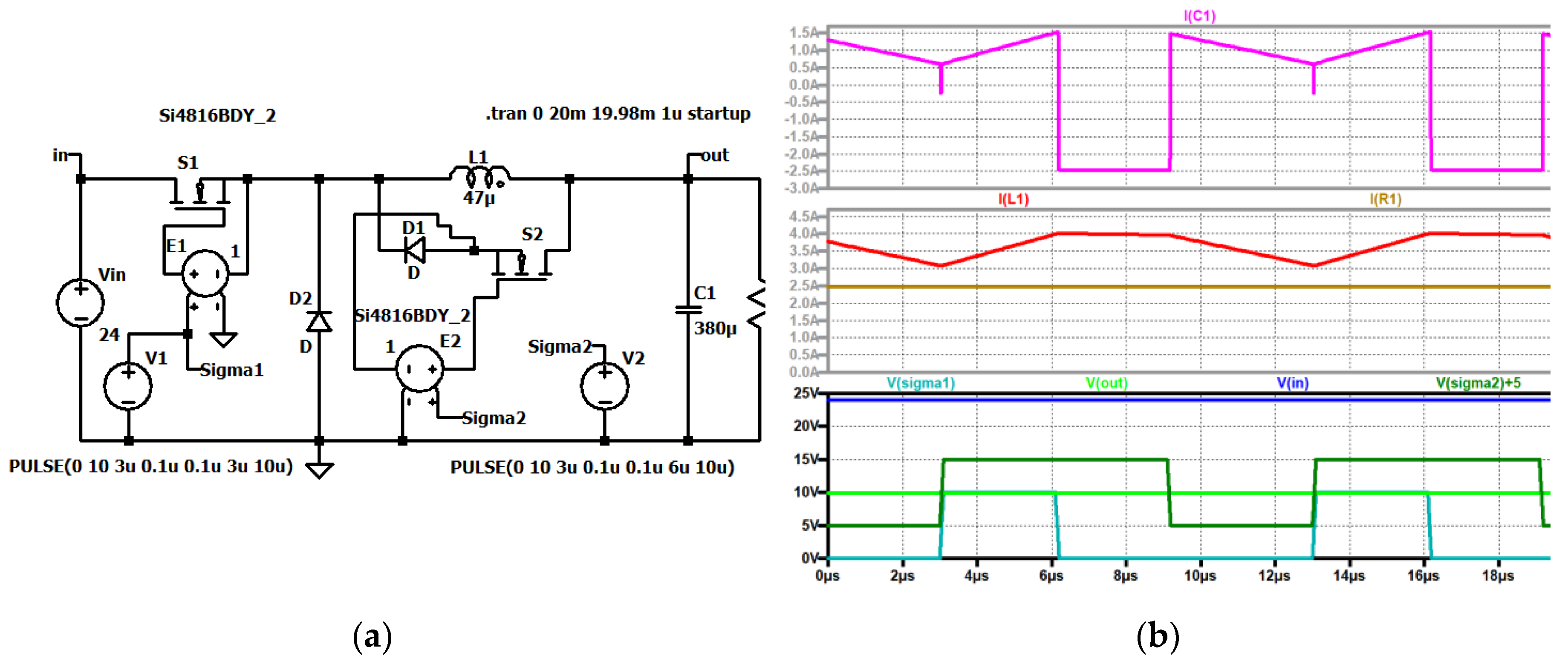
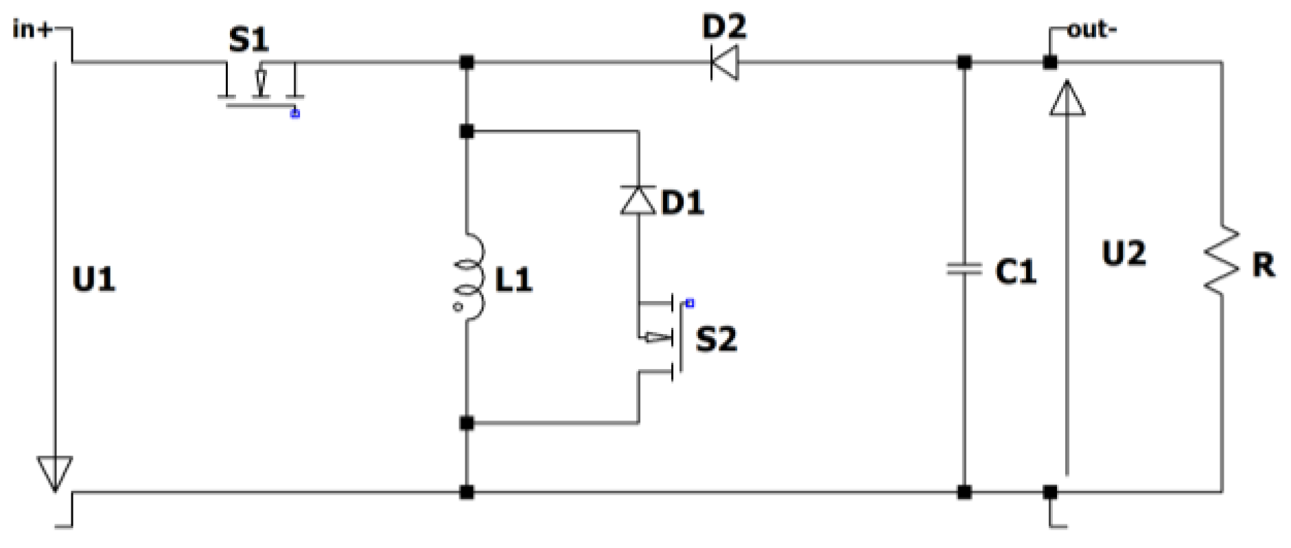
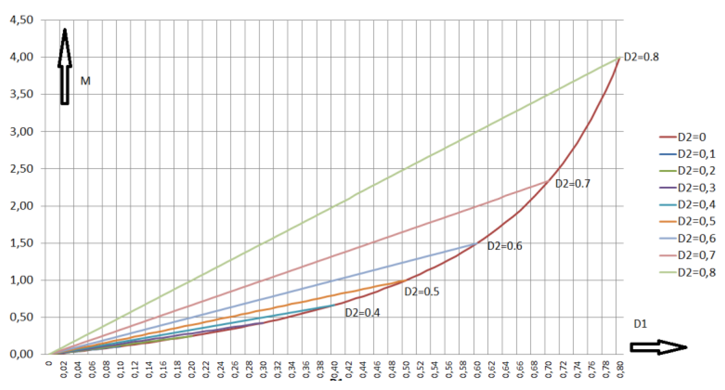
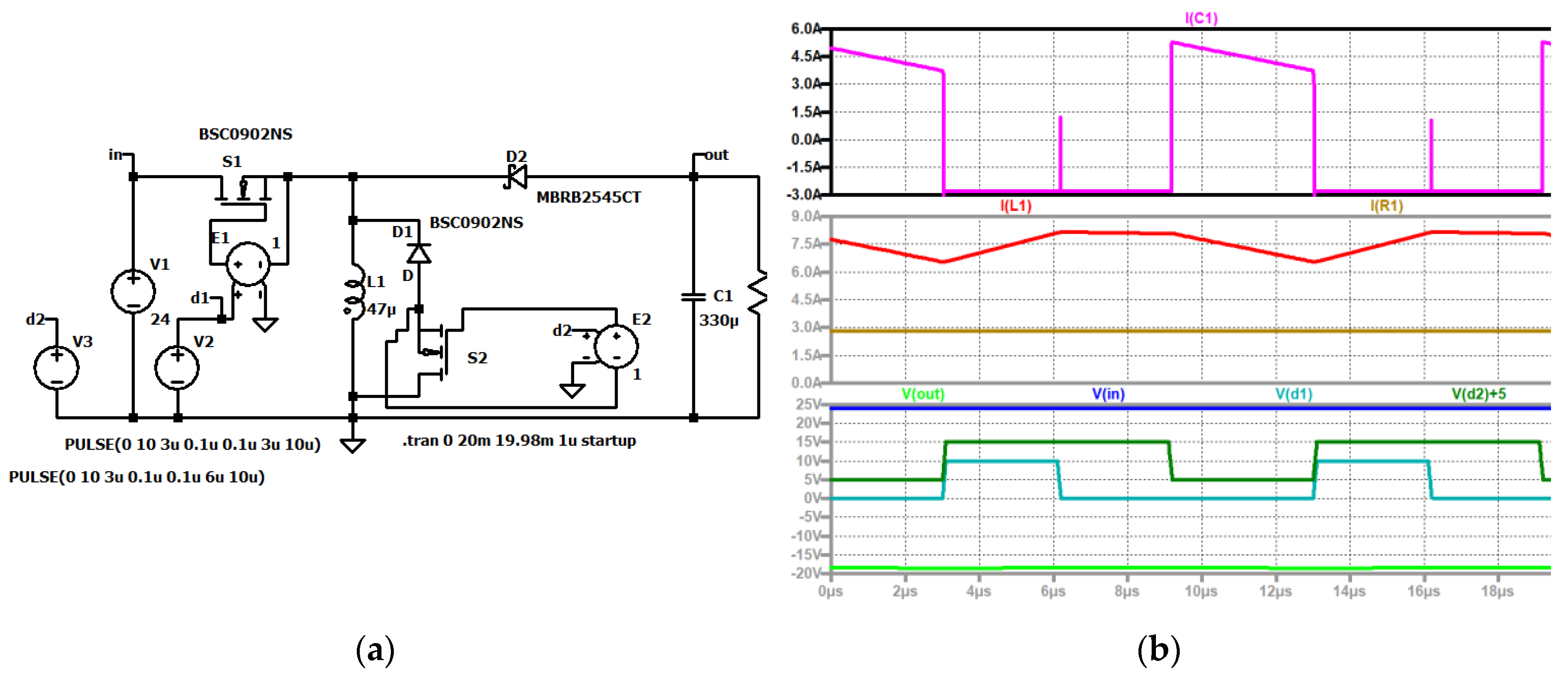
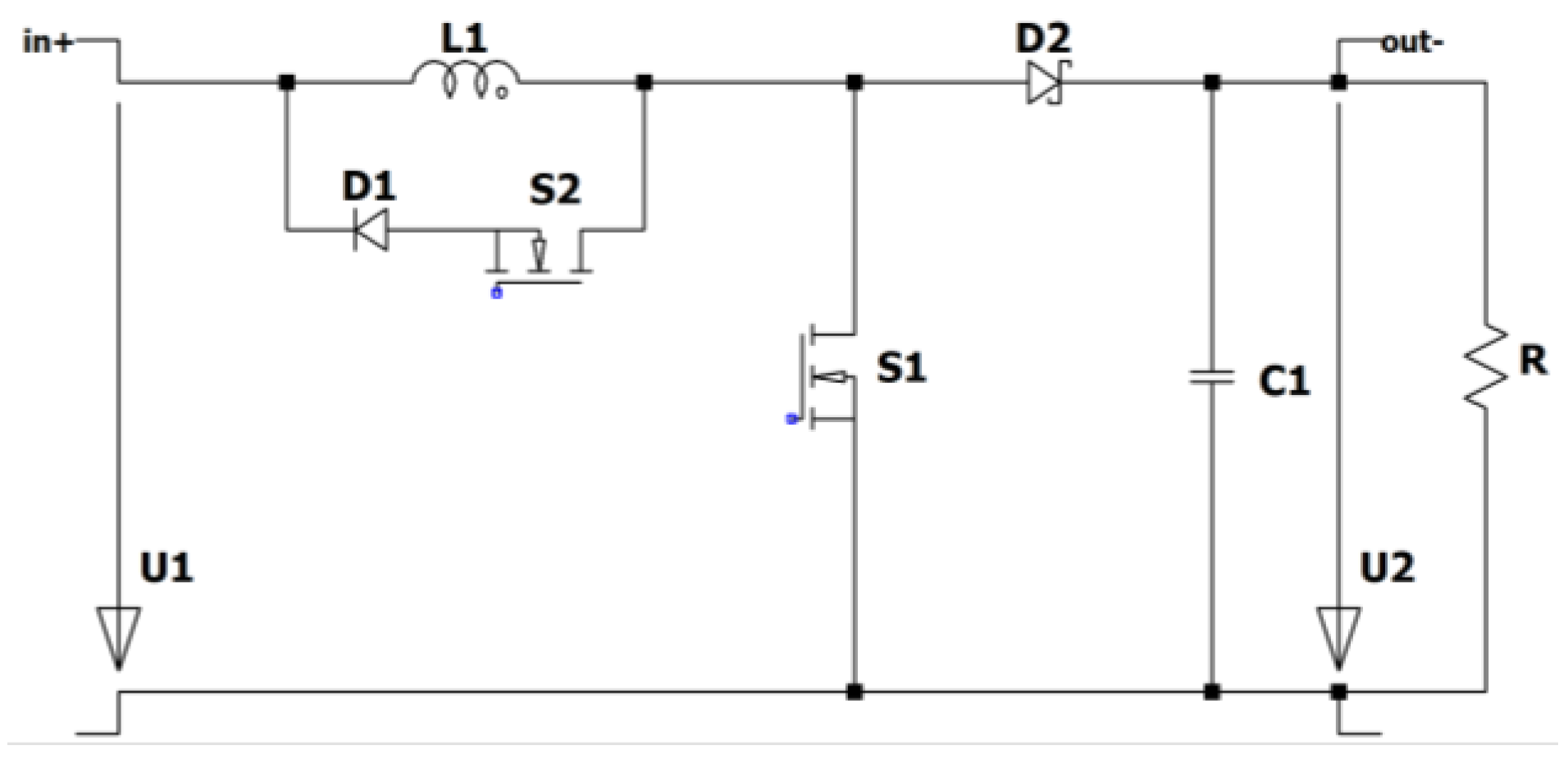
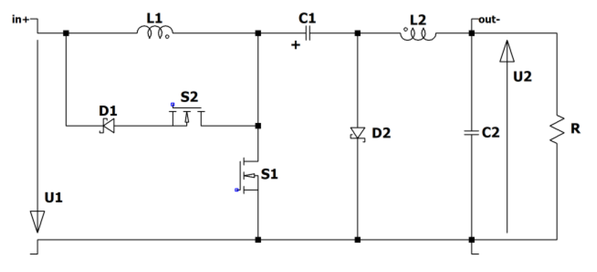
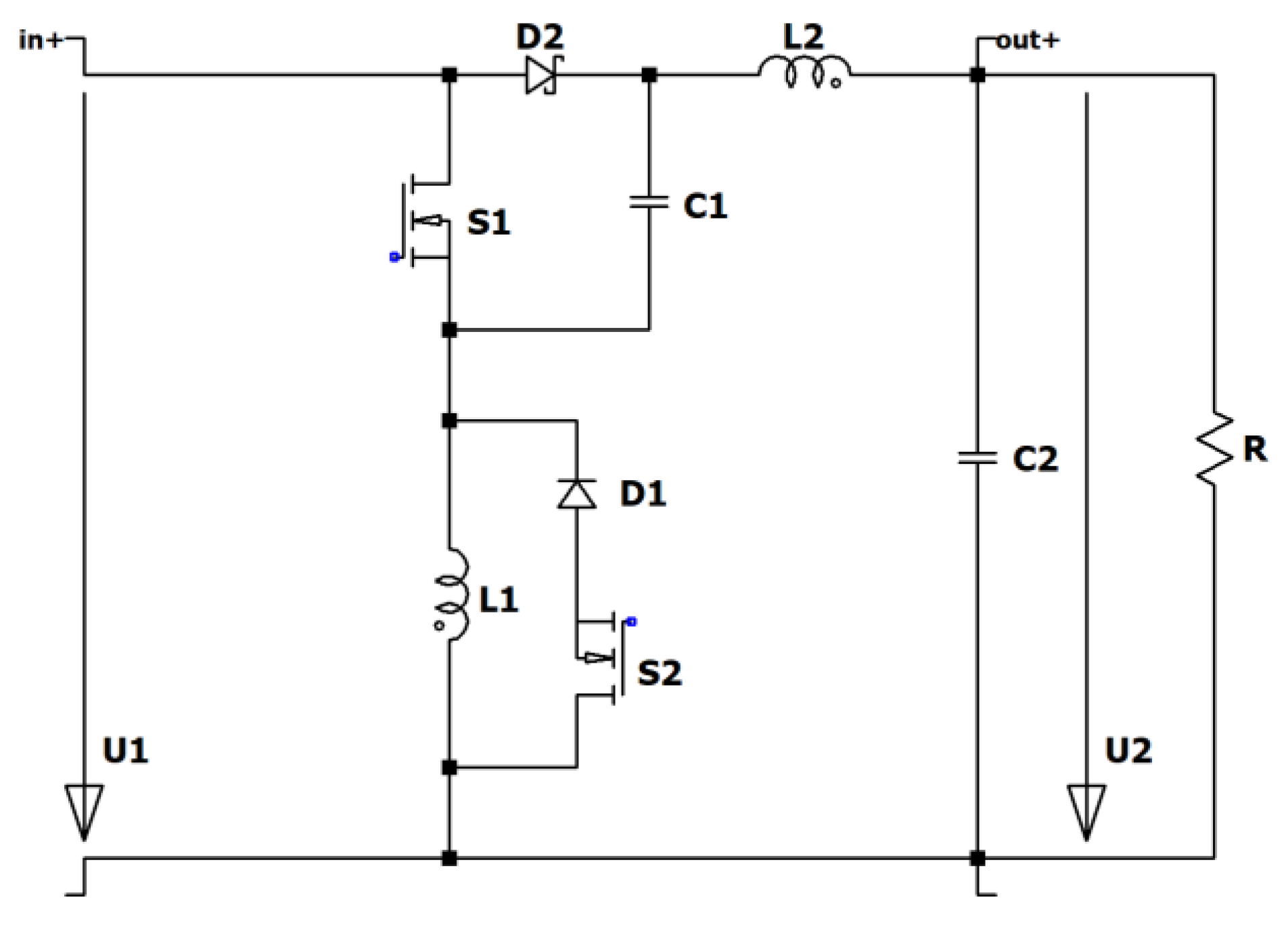
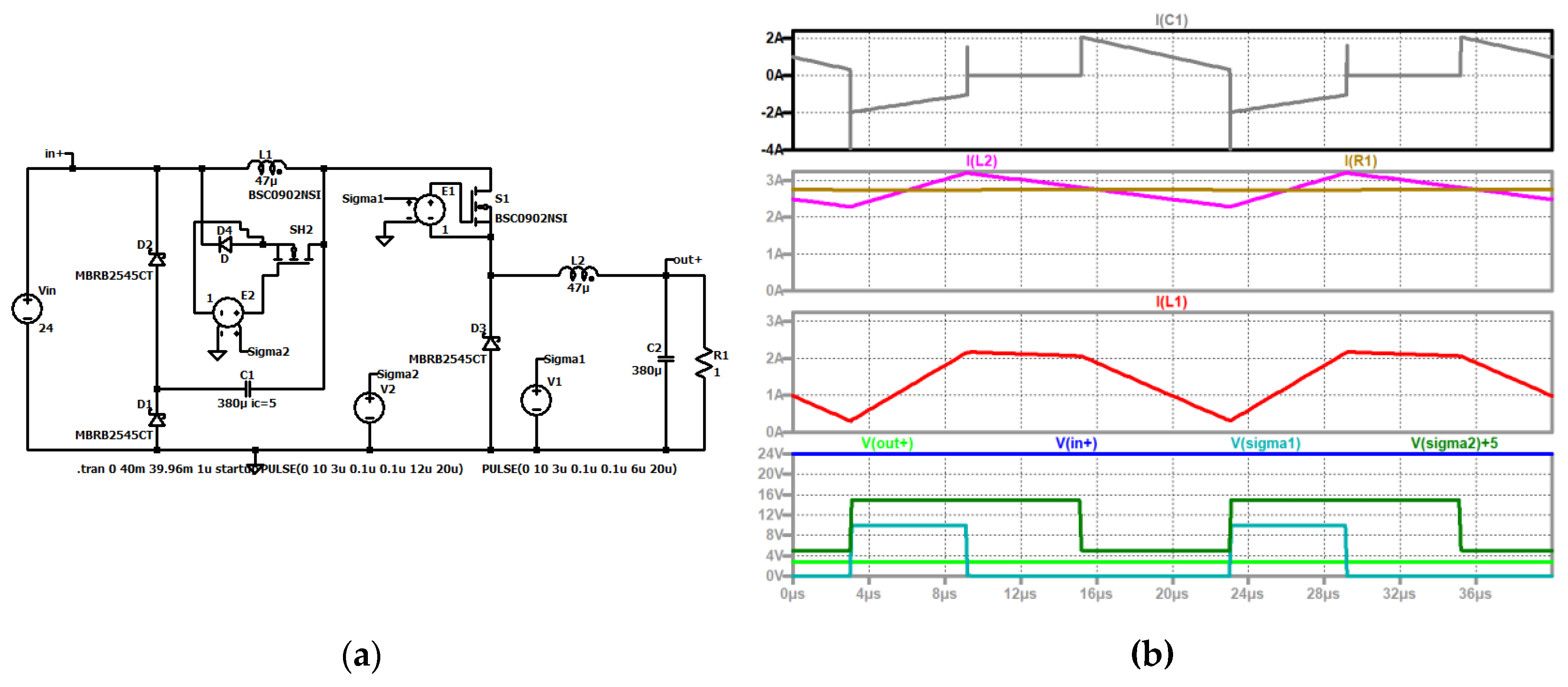
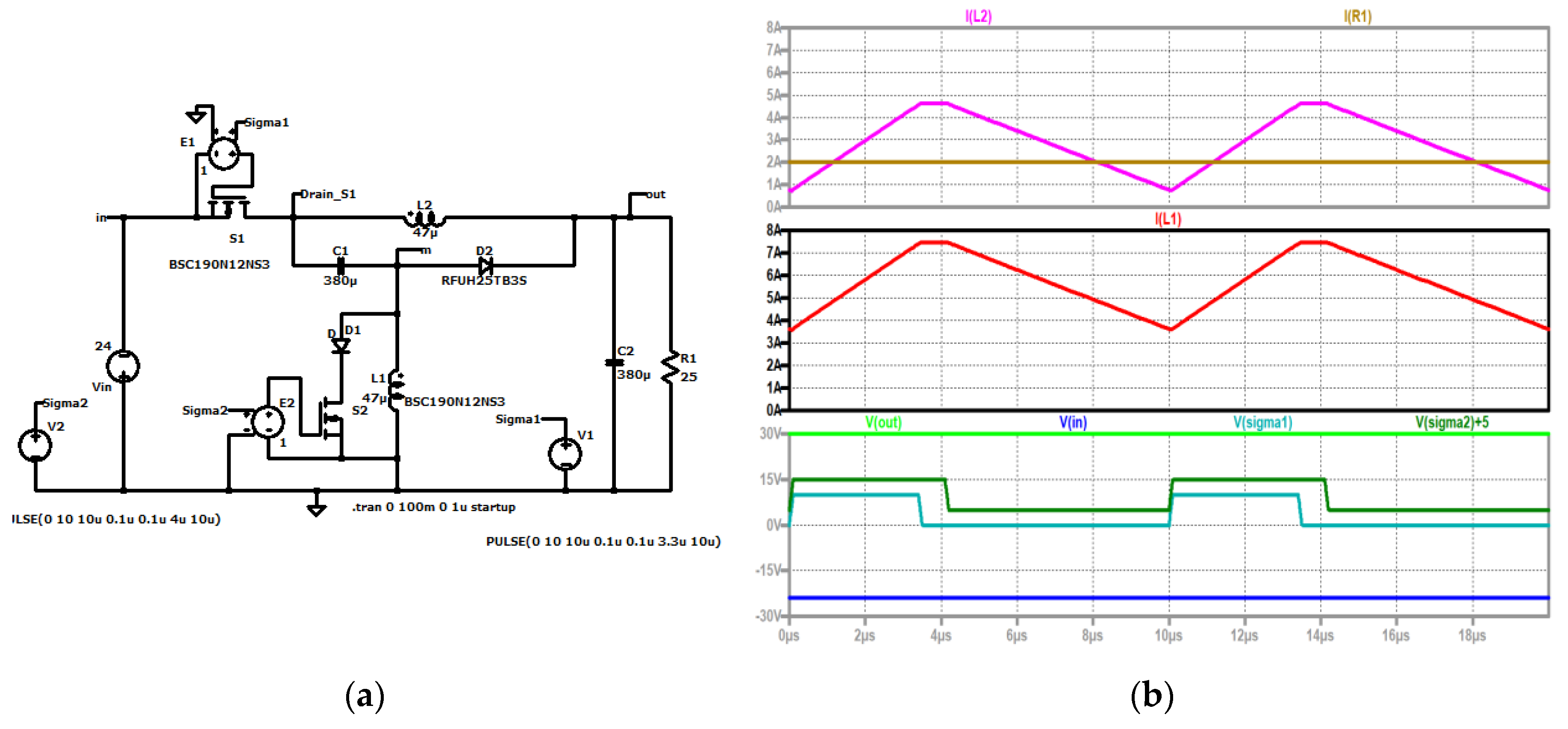
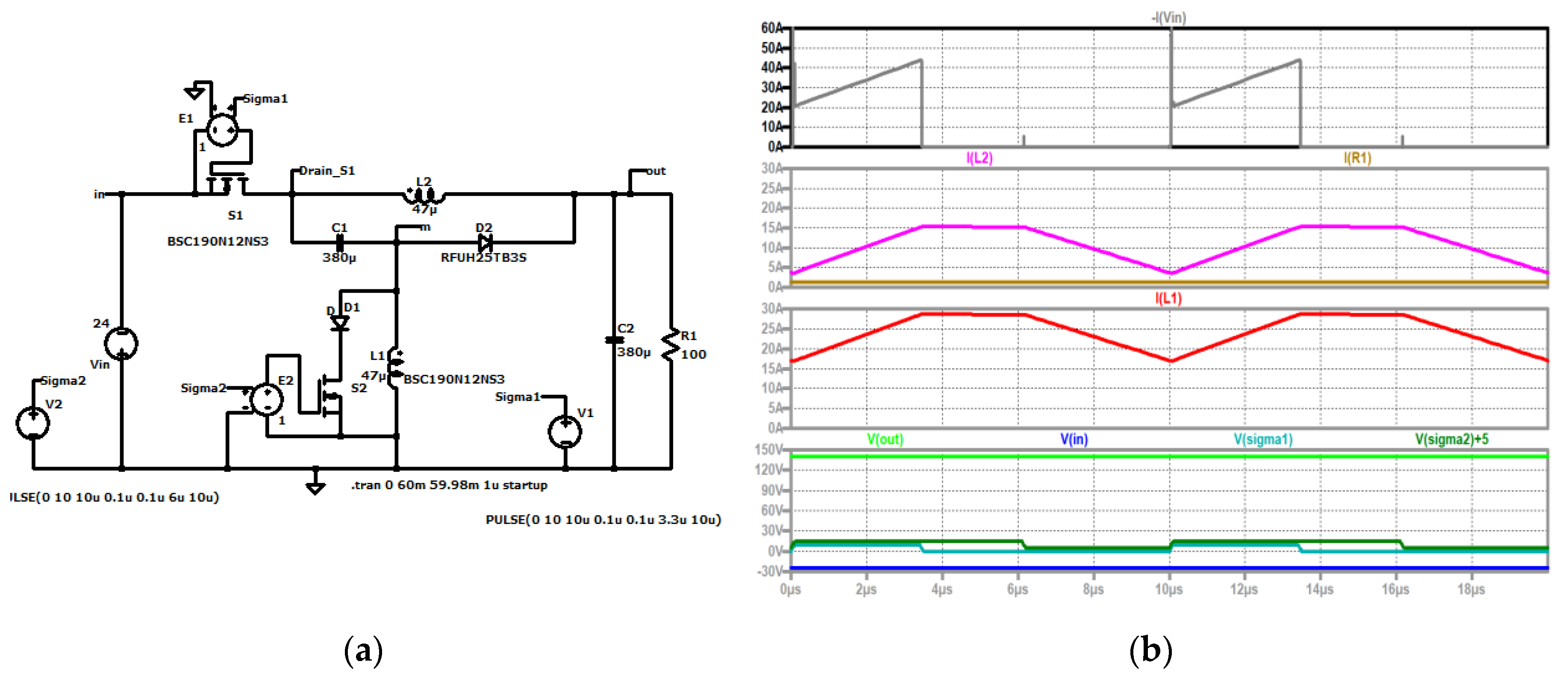
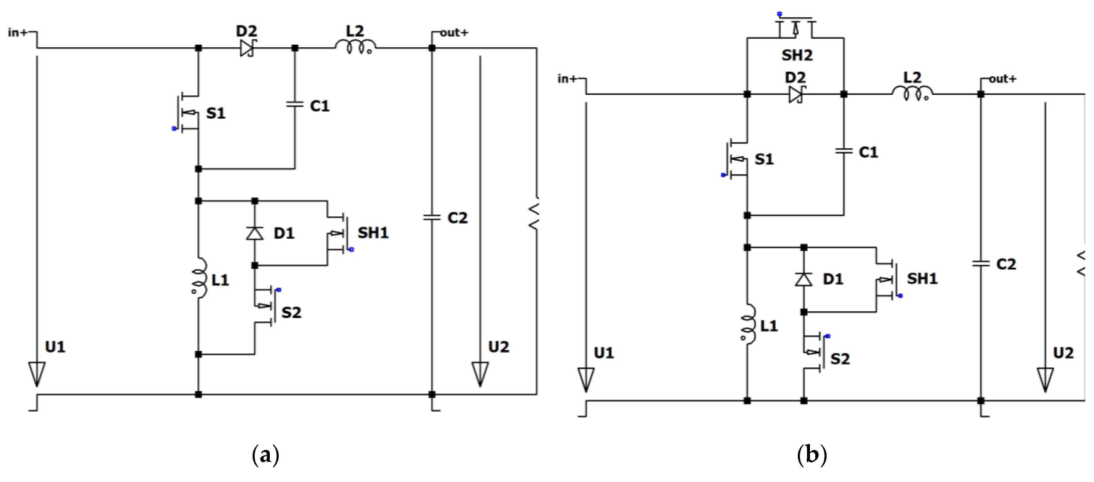
2.1. Reduced Loss Tristate Buck Converter
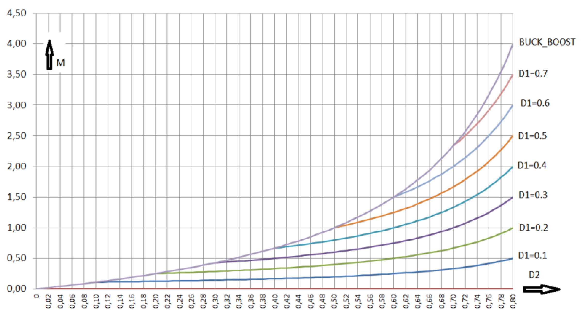
2.2. Reduced Loss Tristate Buck-Boost Converter
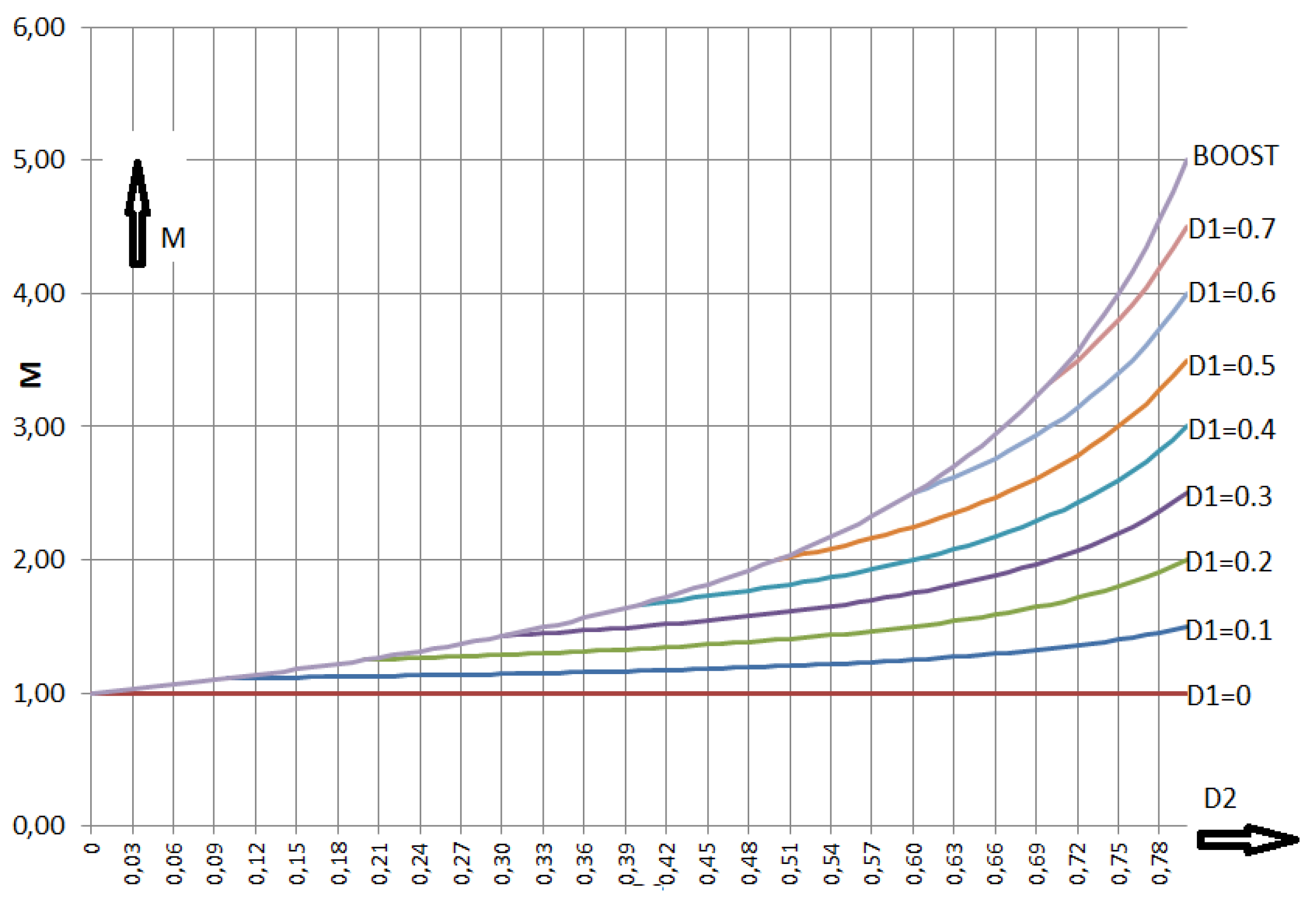
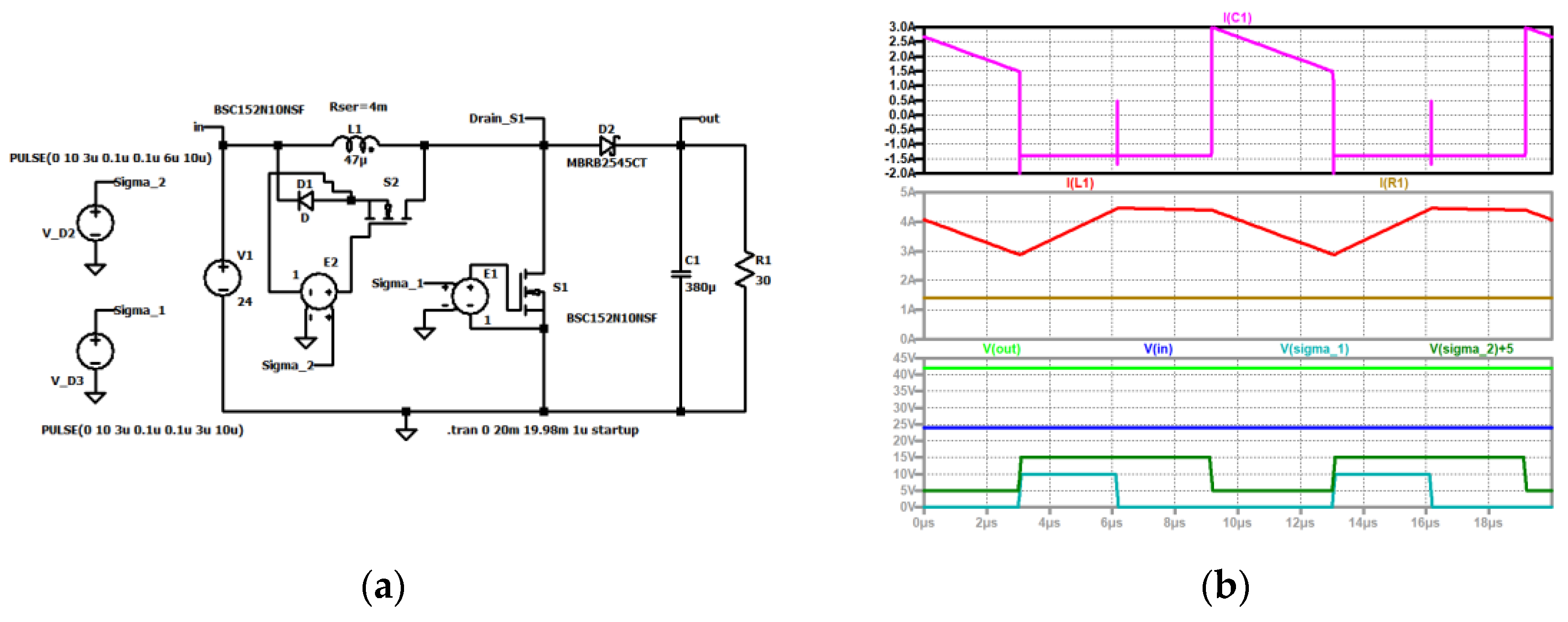
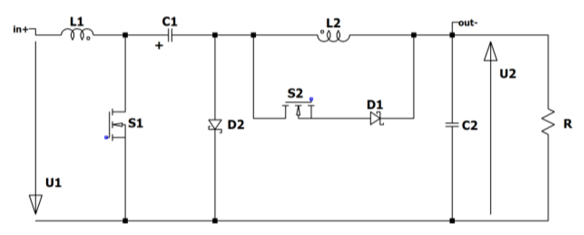
2.3. Reduced Loss Tristate Boost Converter
2.4. Reduced Loss Tristate Zeta Converter
2.5. Reduced Loss Tristate Cuk Converter
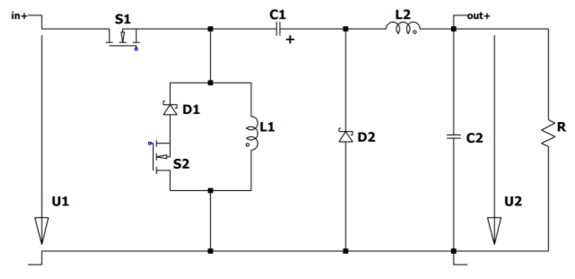
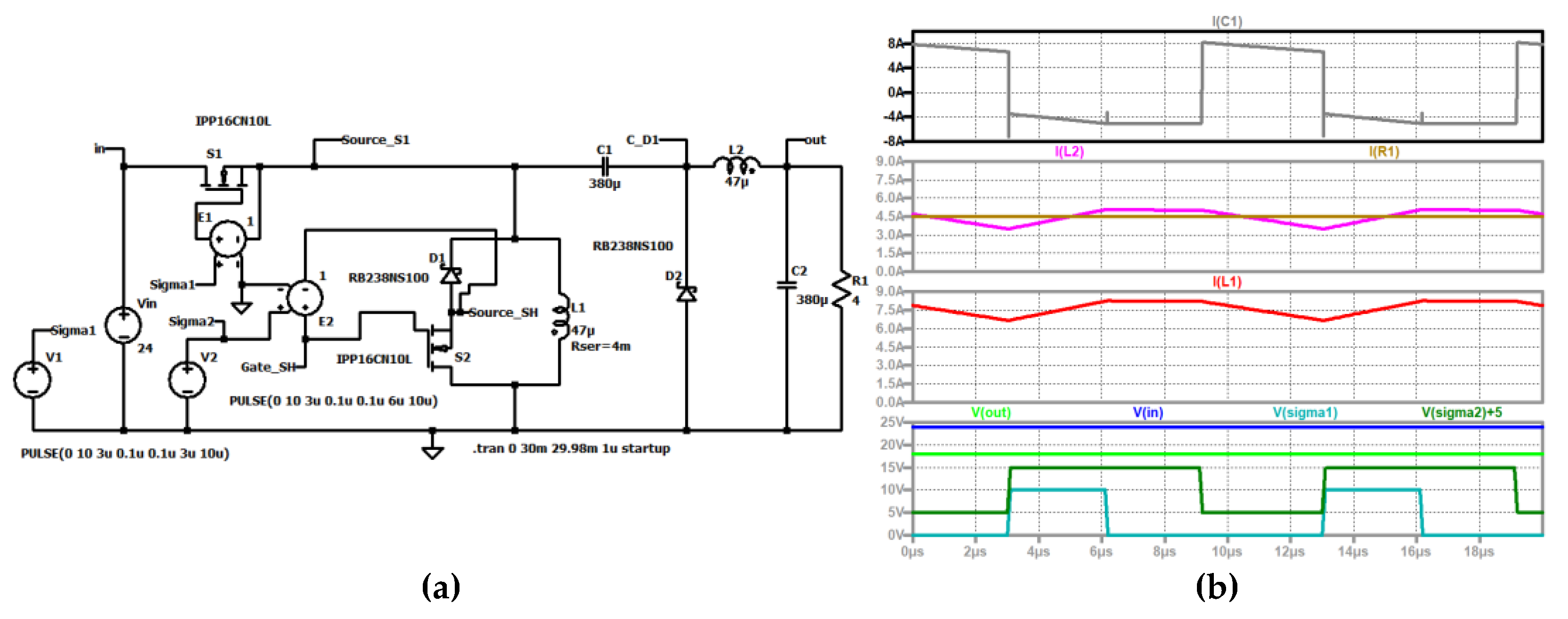
2.6. Reduced Loss Tristate Super-Boost Converter
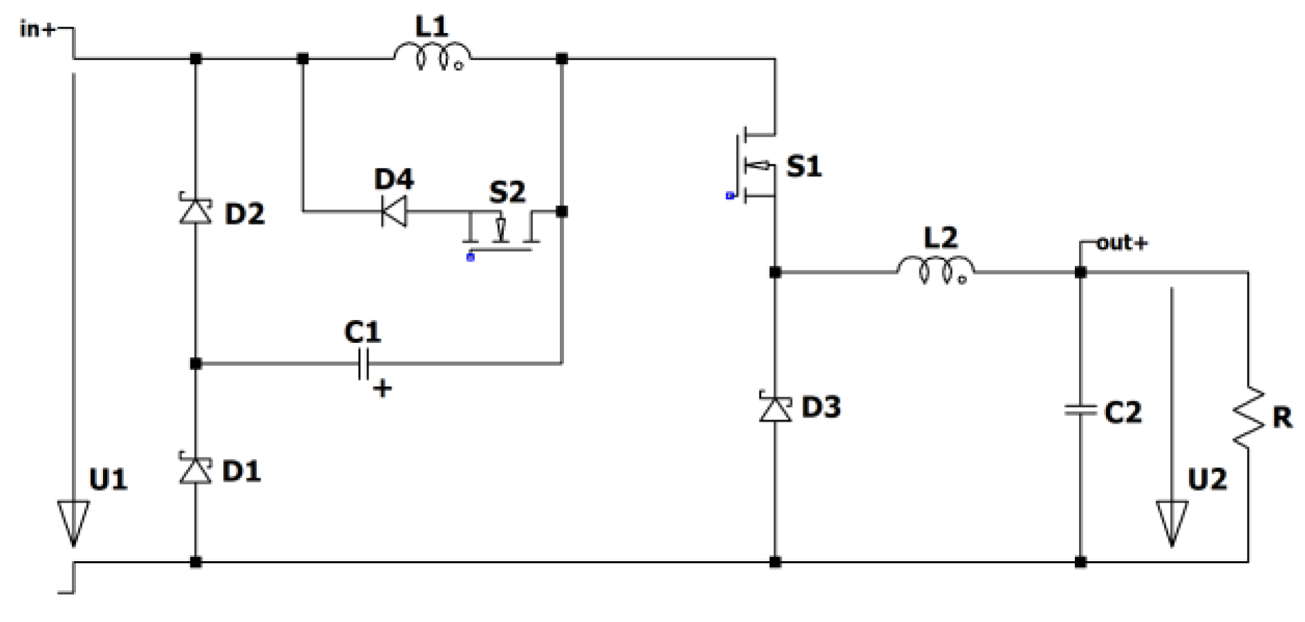
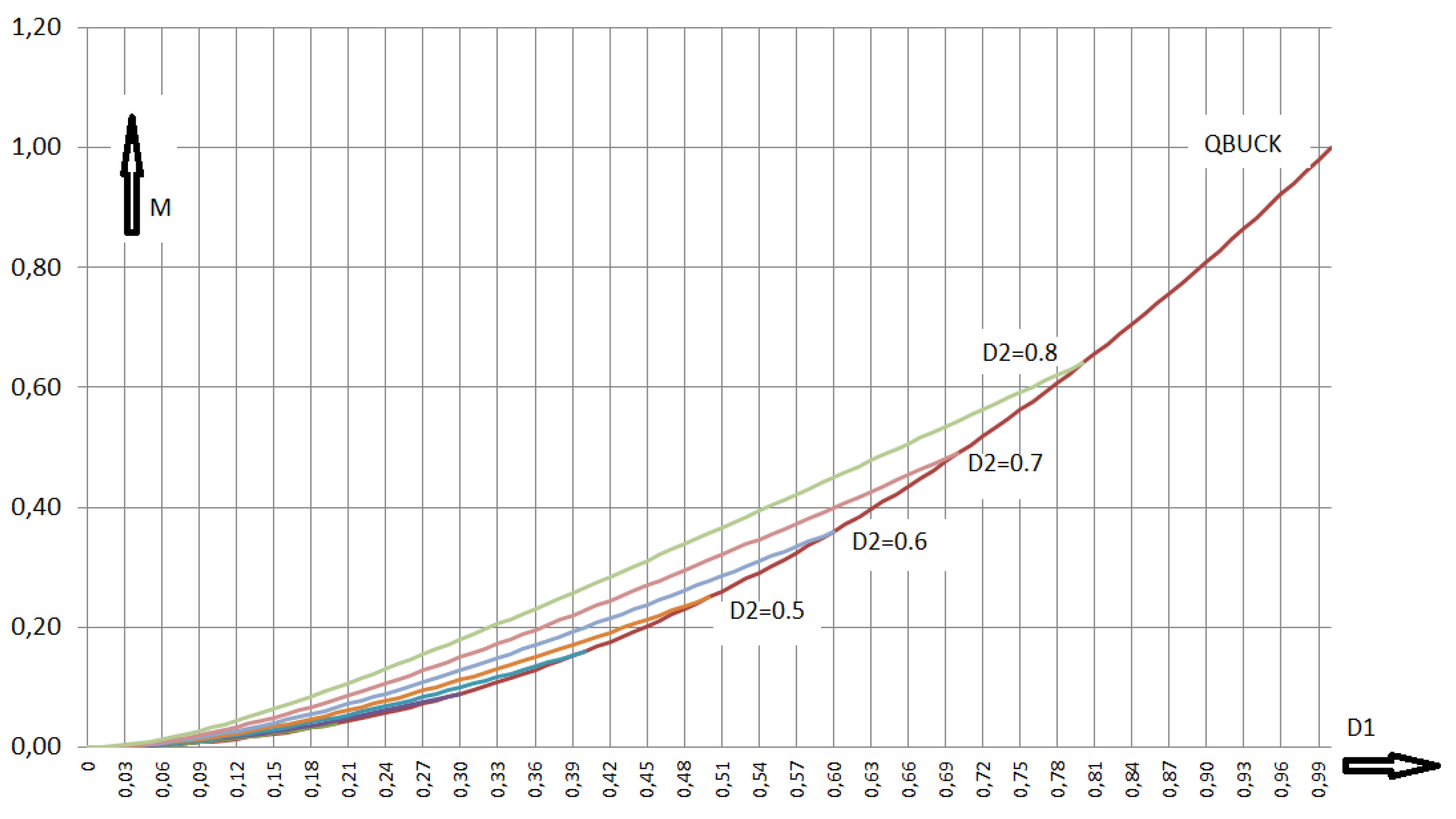
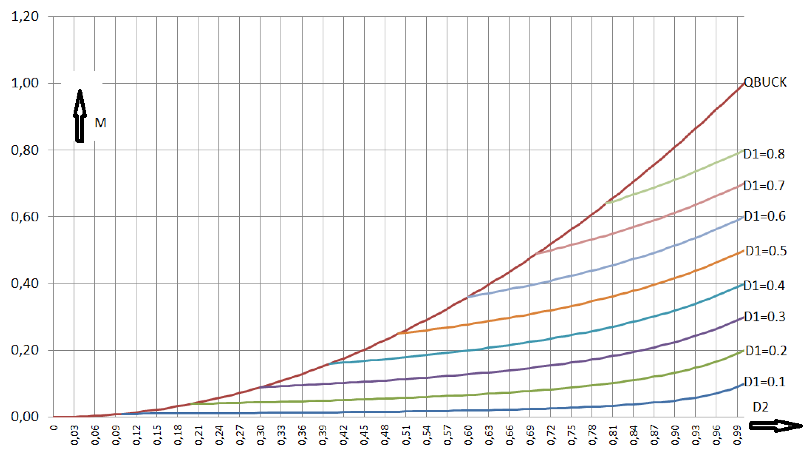
2.7. Reduced Loss Tristate D-Square Buck Converter
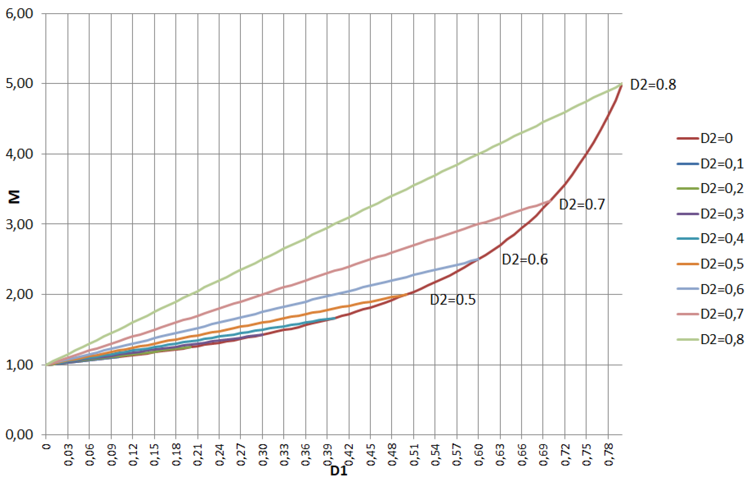
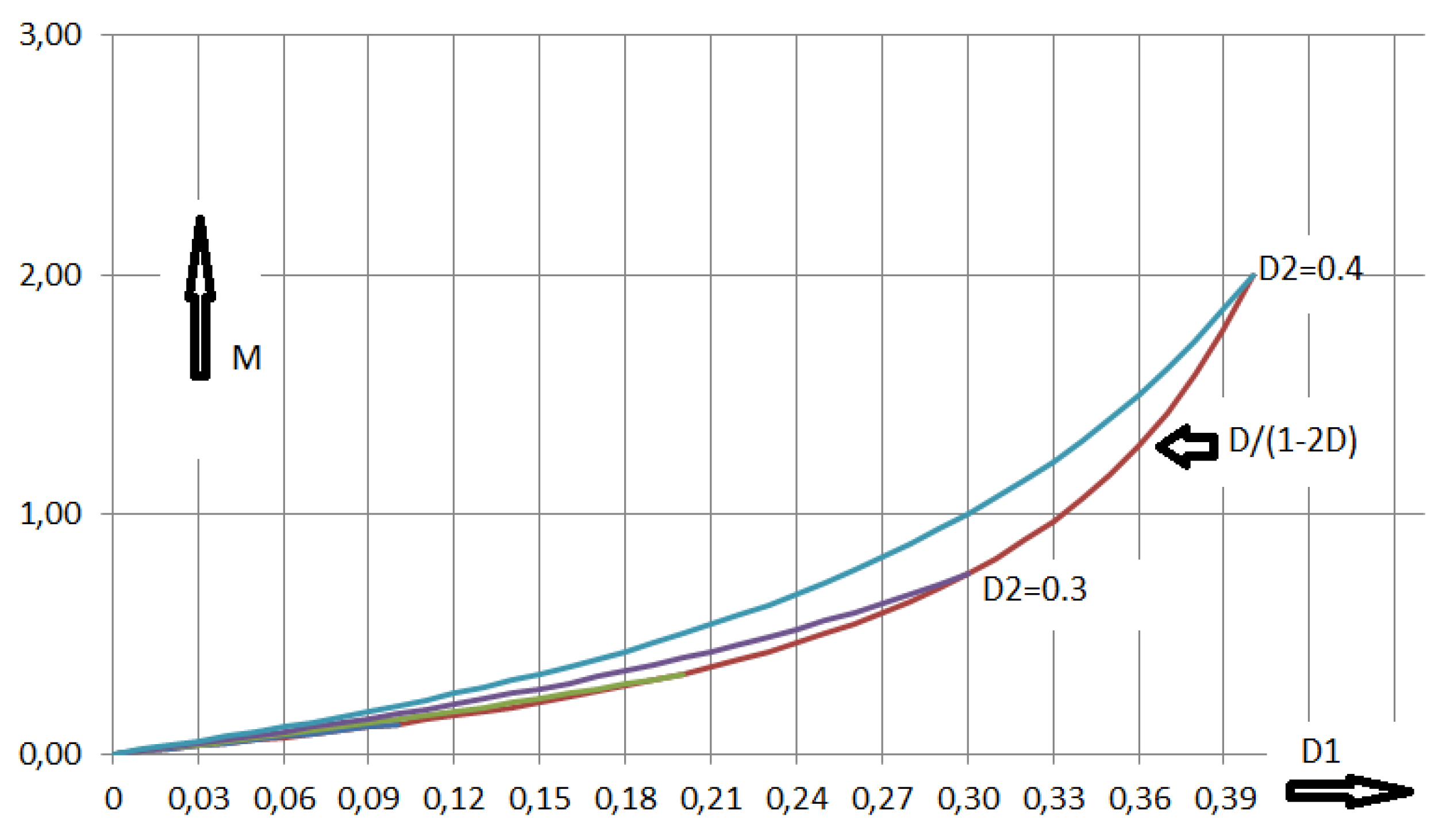
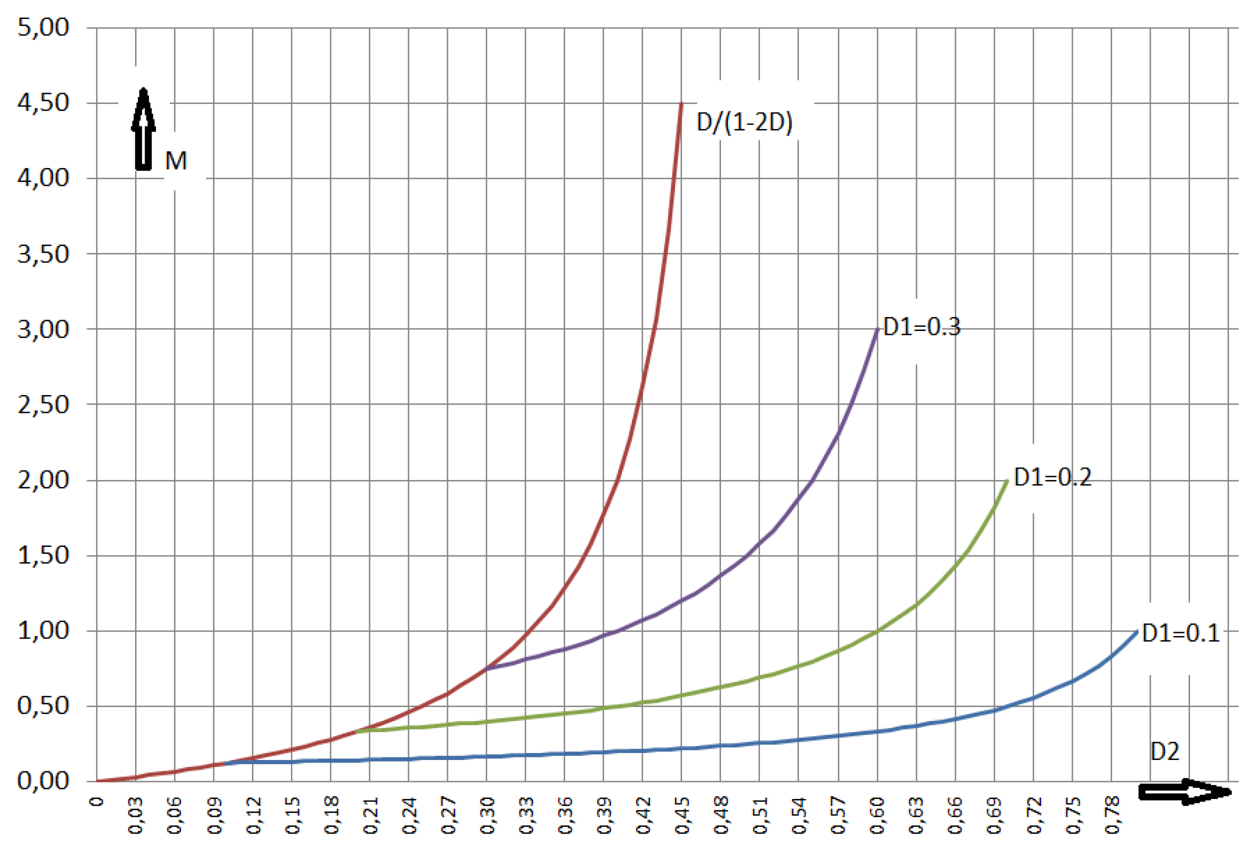
2.8. Reduced Loss Tristate D1/(1-D1-D2) Converter
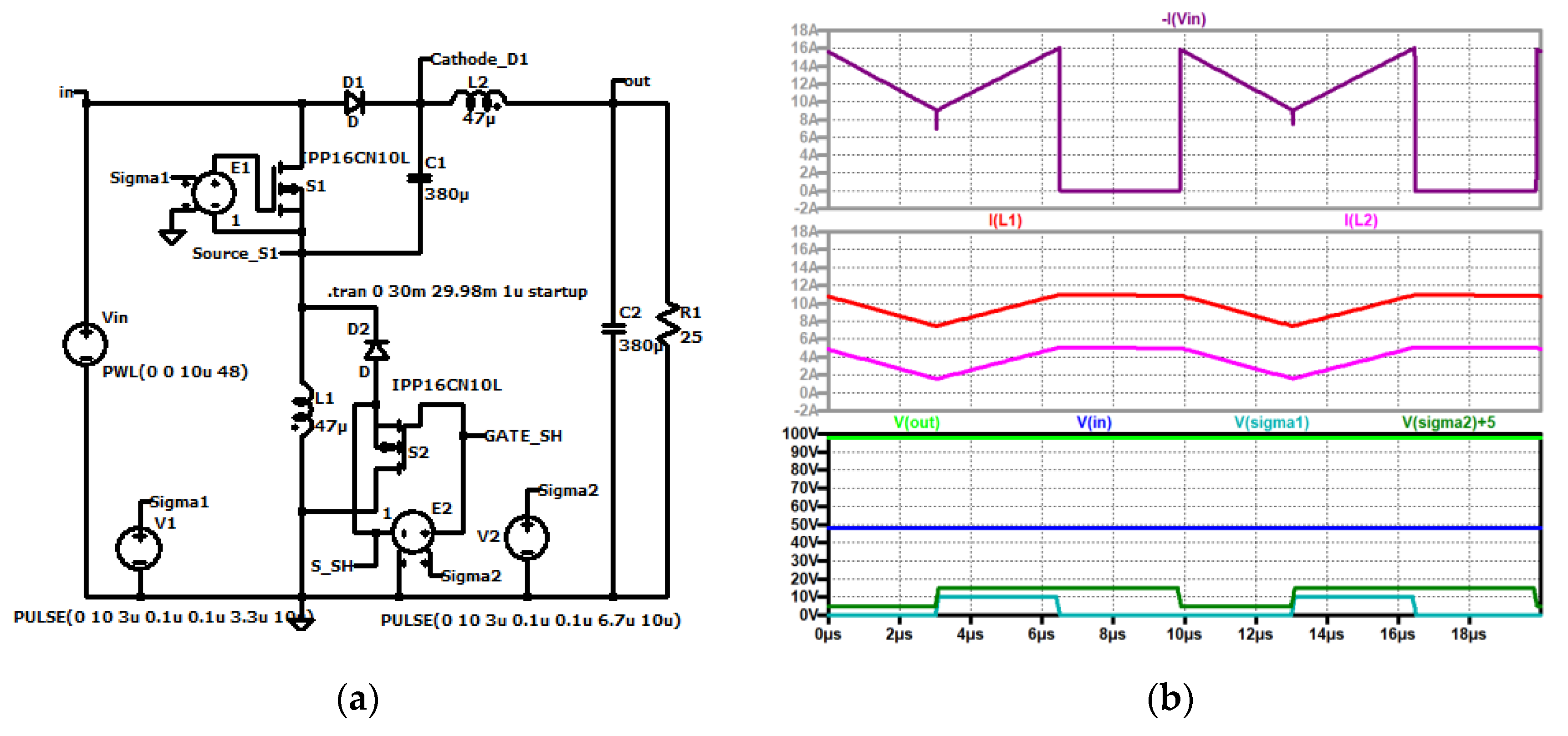
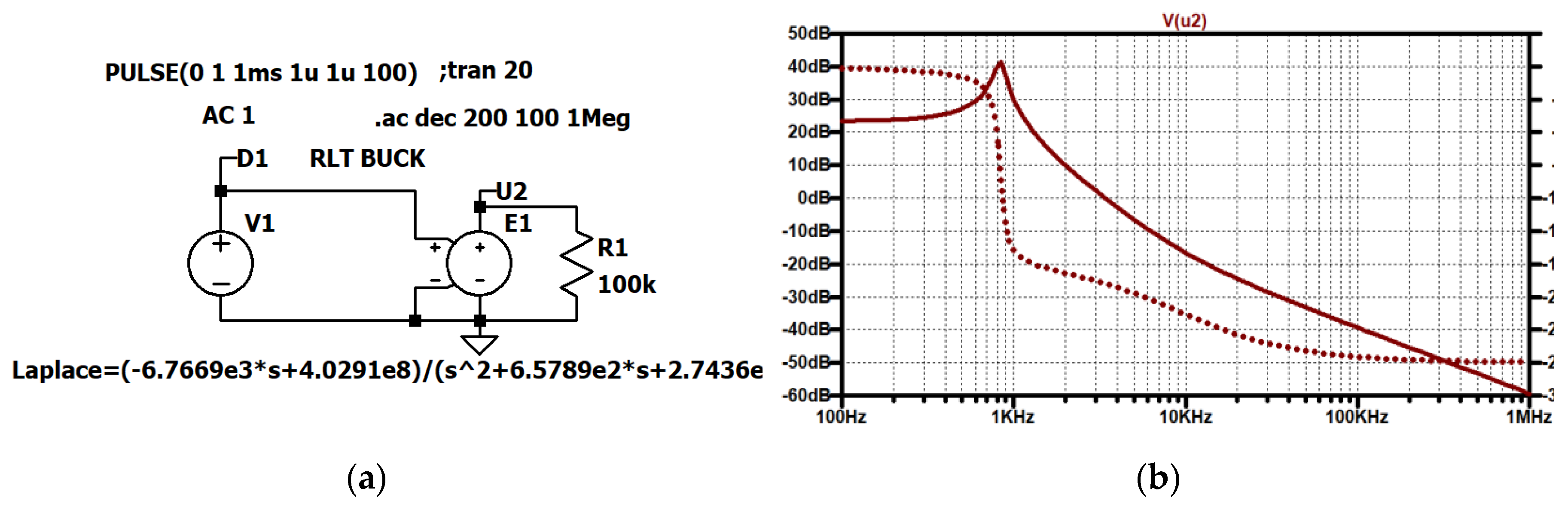
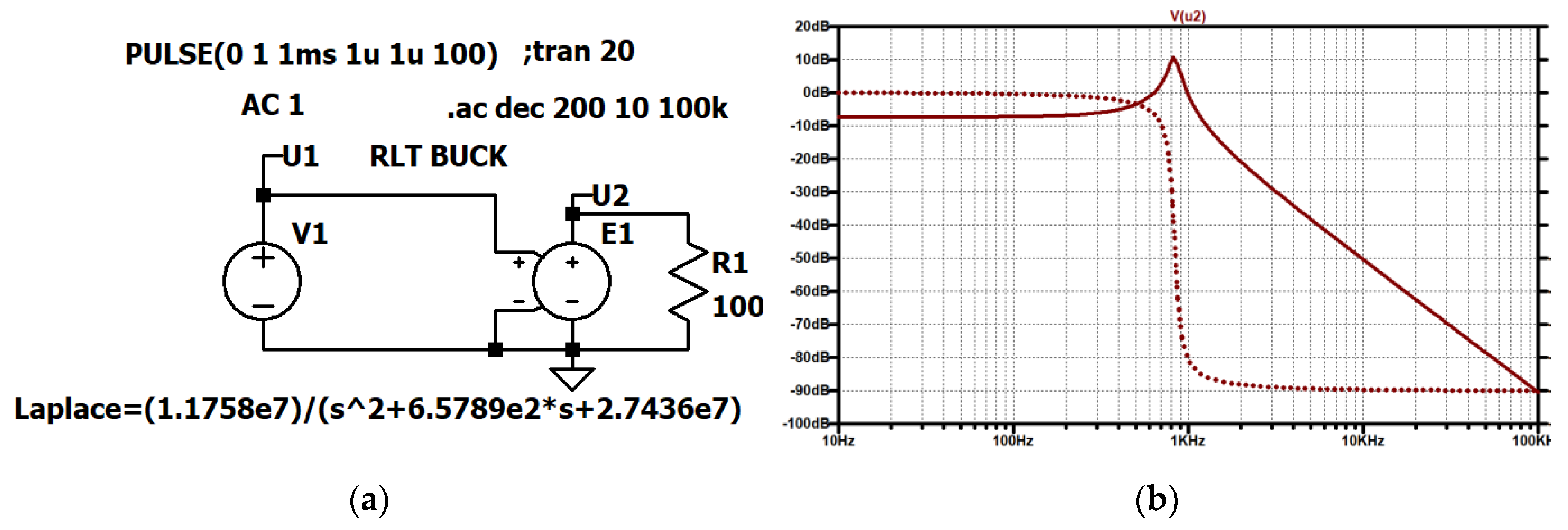
3. RLT Buck Transfer Functions and Bode Diagrams
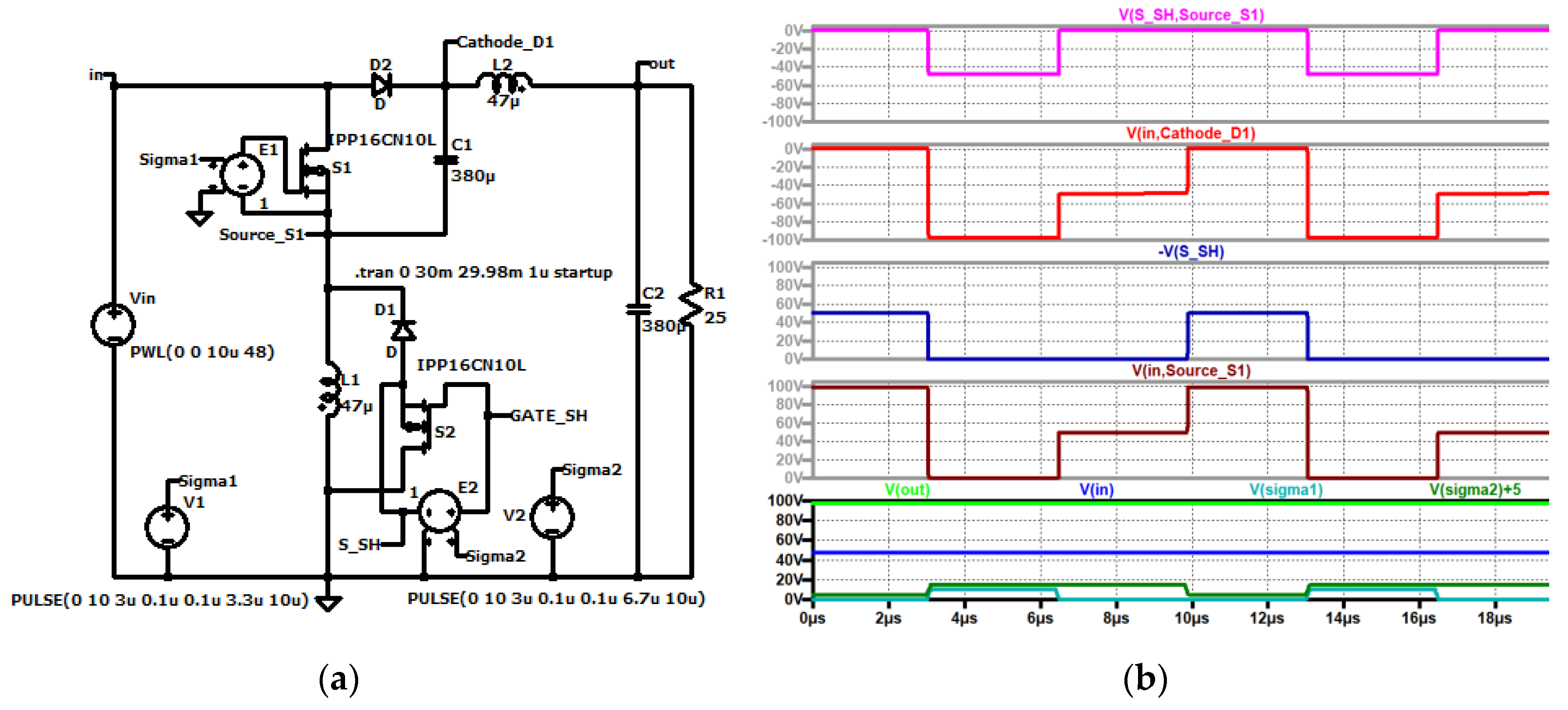
4. Voltage Stress Across the Semiconductors of RLT Converters
4.1. RLT Buck (Figure 3)
4.2. RLT Buck-Boost (Figure 7)
4.3. RLT Boost (Figure 11)
4.4. RLT Zeta (Figure 15)
4.5. RLT Cuk (Figure 17)
4.6. RLT Super Boost (Figure 21)
4.7. RLT D-Square Buck (Figure 24)
4.8. RLT D1/(1-D1-D2) converter (Figure 28)
4.9. Summery voltage stress
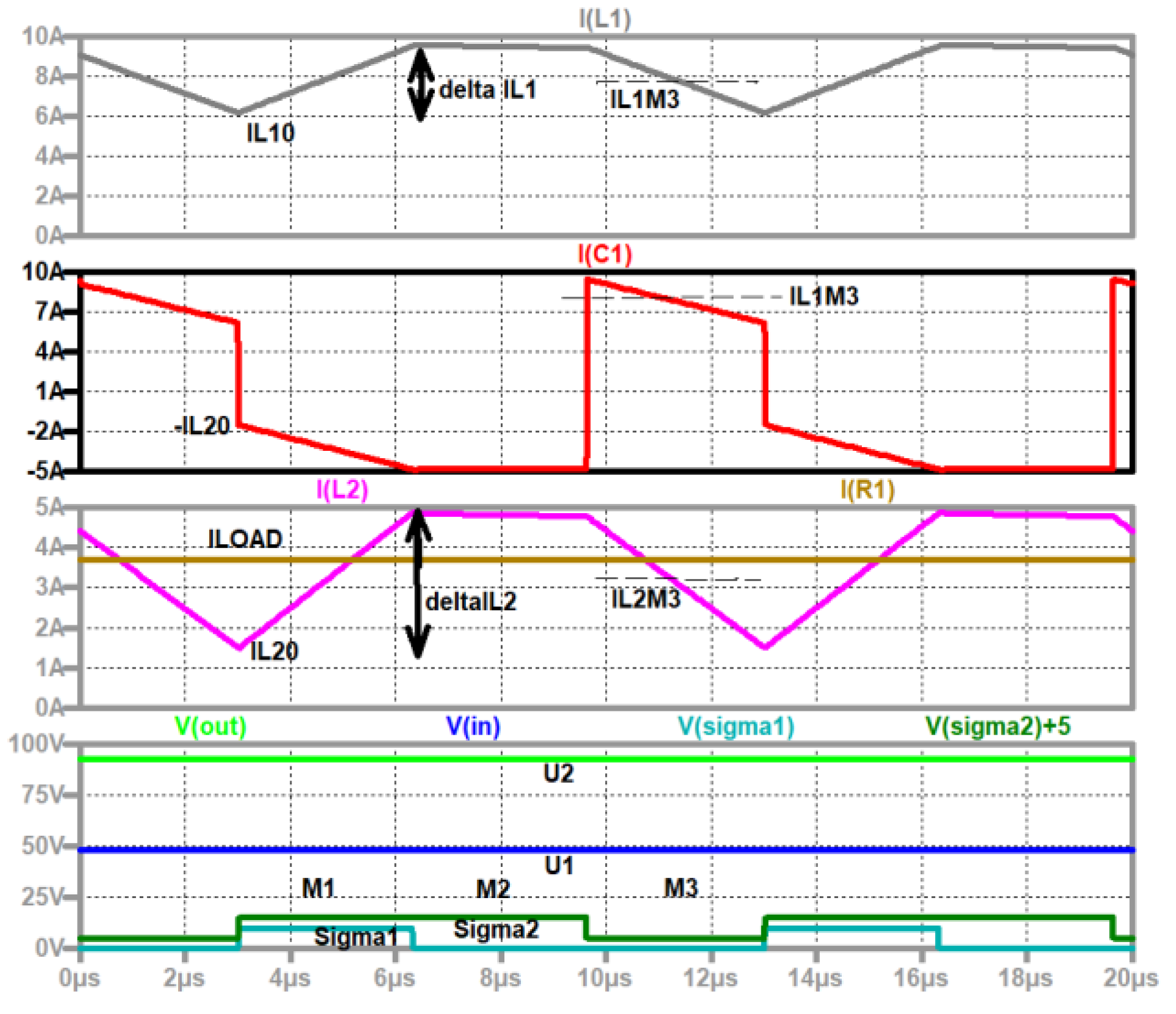
5. Connections Between the Currents
5.1. Simple Approximation of the Currents
5.1.1. Currents Through the Second Order Converters
5.1.2. Currents Through the Fourth Order Converters
5.1.3. Currents Through the d-Square Converter
5.1.4. Currents Through the d1/(1-d1-d2) Converter
5.2. Onward Losses
5.3. Reduction of the loss compared to the traditional tristate converter
5.4. Input and Output Currents
5.5. Precise Calculation of the Currents
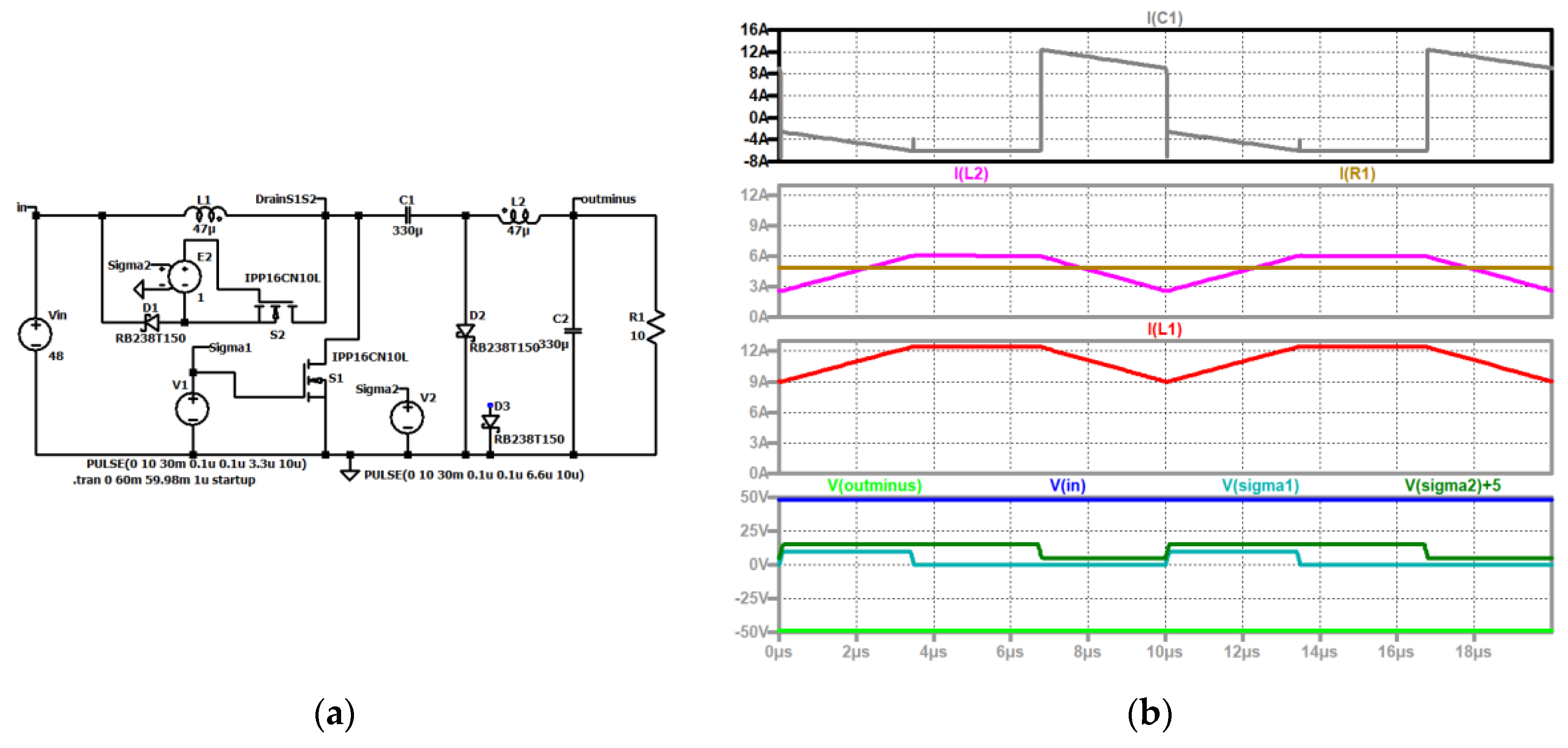
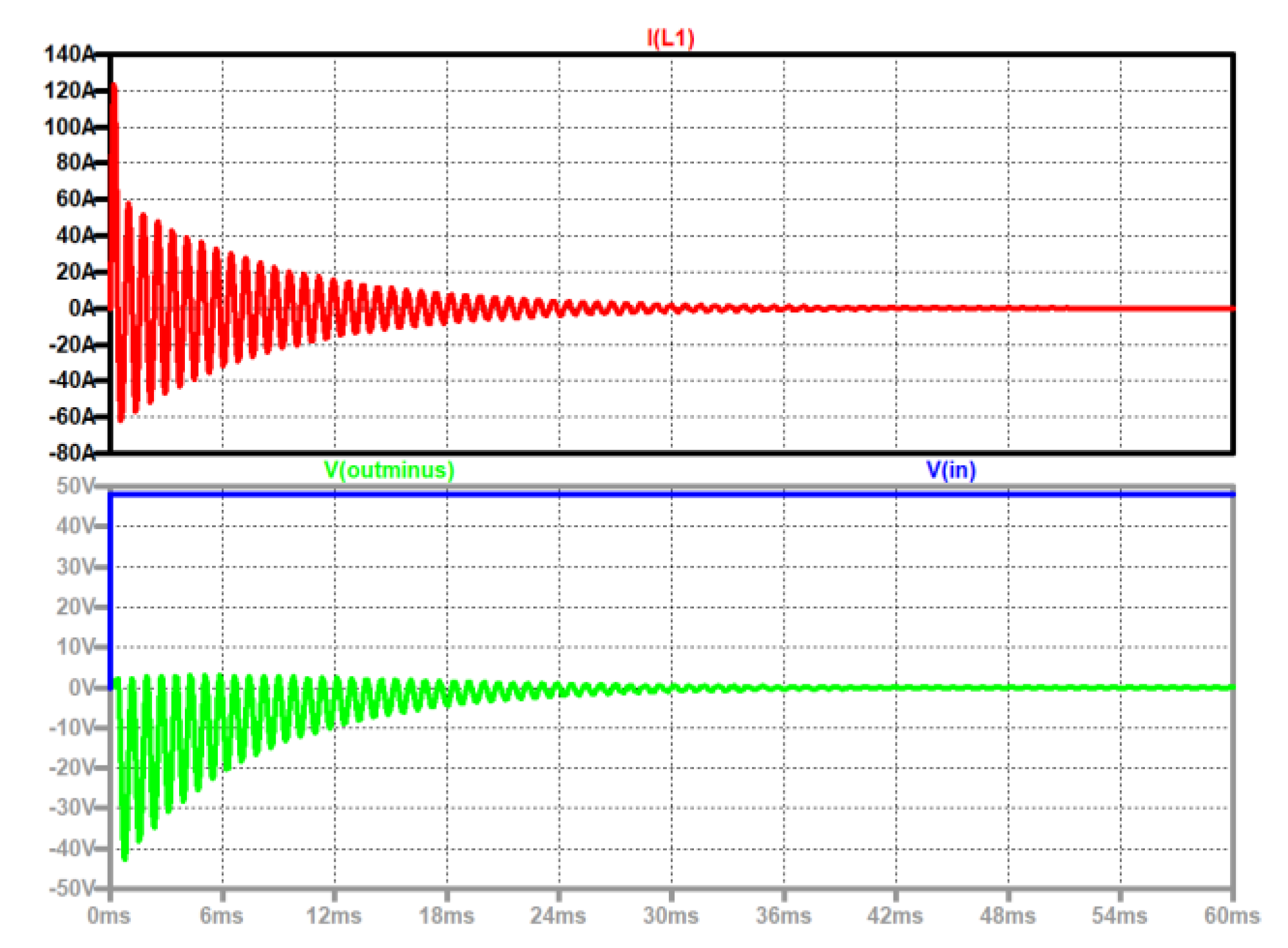
5.6. Inrush currents
5. Conclusion
Author Contributions
Funding
Data Availability Statement
Conflicts of Interest
References
- Mohan, N.; Undeland, T.; Robbins, W. Power Electronics, Converters, Applications and Design, New York: W. P. John Wiley & Sons.
- Rozanov, Y.; Ryvkin, S.; Chaplygin, E.; Voronin, P. Power Electronics Basics, CRC Press.
- (text in German), F. Zach, Leistungselektronik, Frankfurt: Springer, 6th ed. 2022.
- Cuk, S. General topological properties of switching structures, IEEE Power Electronics Specialists Conference, San Diego, CA, USA, 1979, pp. 109-130.
- Forouzesh, M.; Siwakoti, Y.P.; Gorji, S.A.; Blaabjerg, F.; Lehman, B. Step-Up DC–DC Converters: A Comprehensive Review of Voltage-Boosting Techniques, Topologies, and Applications, IEEE Transactions on Power Electronics, vol. 32, no. 12, pp. 9143-9178, Dec. 2017. [CrossRef]
- Williams, B.W. Generation and Analysis of Canonical Switching Cell DC-to-DC Converters, IEEE Transactions on Industrial Electronics, vol. 61, no. 1, pp. 329-346, Jan. 2014. [CrossRef]
- Marquez, R.; Contreras-Ordaz, M.A. The Three-Terminal Converter Cell, Graphs, and Generation of DC-to-DC Converter Families. IEEE Transactions on Power Electronics 2020, 35, 7725–7728. [Google Scholar] [CrossRef]
- Himmelstoss, F.A. Fourth order DC-DC converters with limited duty cycle range, Proceedings of Intelec 93: 15th International Telecommunications Energy Conference, Paris, France, 1993, pp. 358-364 vol.1. [CrossRef]
- Viswanathan, K.; Oruganti, R.; Srinivasan, D. A novel tri-state boost converter with fast dynamics, IEEE Transactions on Power Electronics, vol. 17, no. 5, pp. 677-683, Sept. 2002. [CrossRef]
- Himmelstoss, F.A.; Converters, T. WSEAS TRANSACTIONS on POWER SYSTEMS, Volume 18, 2023, pp. 259-269, E-ISSN: 2224-350X. [CrossRef]
- Vaghela, G.M.A.; Mulla, M.A. Tri-State Coupled Inductor Based High Step-Up Gain Converter Without Right Hand Plane Zero, IEEE Transactions on Circuits and Systems II: Express Briefs, vol. 70, no. 6, pp. 2291-2295, 23. 20 June. [CrossRef]
- Viswanathan, K.; Oruganti, R.; Srinivasan, D. Tri-state boost converter with no right half plane zero, 4th IEEE International Conference on Power Electronics and Drive Systems. IEEE PEDS 2001 - Indonesia. Proceedings (Cat. No.01TH8594), Denpasar, Indonesia, 2001, pp. 687-693 vol.2.
- Kapat, S.; Patra, A.; Banerjee, S. A novel current controlled tri-state boost converter with superior dynamic performance, 2008 IEEE International Symposium on Circuits and Systems, Seattle, WA, USA, 2008, pp. 2194-2197.
- Rana, N.; Banerjee, S. Interleaved Tri-state Buck-Boost Converter with Fast Transient Response and Lower Ripple, 2019 IEEE Transportation Electrification Conference (ITEC-India), Bengaluru, India, 2019, pp. 1-5.
- Knecht, O.; Bortis, D.; Kolar, J.W. ZVS Modulation Scheme for Reduced Complexity Clamp-Switch TCM DC–DC Boost Converter. IEEE Transactions on Power Electronics 33, 4204–4214. [CrossRef]
- Maksimovic, D. and S. Cuk: Switching converters with wide DC conversion range, IEEE Transactions on Power Electronics. IEEE Transactions on Power Electronics 1991, 6, 151–157. [Google Scholar] [CrossRef]
- Sarkar, S.; Ghosh, S.S. Traditional IMC & IMC Based PID Controller Design for Tri-State Boost Converter, 2020 IEEE 9th Power India International Conference (PIICON), Sonepat, India, 2020, pp. 1-6. [CrossRef]
- Viswanathan, S.K.; Oruganti, R.; Srinivasan, D. “Dual mode control of tri-state boost converter for improved performance,” IEEE 34th Annual Conference on Power Electronics Specialist, 2003. PESC ’03. Acapulco, Mexico, 2003, pp. 944-950 vol.2. [CrossRef]
- Michal, V.; Cottin, D.; Arno, P. Boost DC/DC converter nonlinearity and RHP-zero: Survey of the control-to-output transfer function linearization methods, 2016 International Conference on Applied Electronics (AE), Pilsen, Czech Republic, 2016, pp. 1-10. [CrossRef]
- Rana, N.; Ghosh, A.; Banerjee, S. Development of an Improved Tristate Buck–Boost Converter With Optimized Type-3 Controller, IEEE Journal of Emerging and Selected Topics in Power Electronics, vol. 6, no. 1, pp. 400-415, 18. 20 March. [CrossRef]
- Karan, R.; Mishra, S.; Kumar, M. Analysis of Non-Isolated Dual Output Tristate Converter for Low Voltage DC Bus, 2024 Third International Conference on Power, Control and Computing Technologies (ICPC2T), Raipur, India, 2024, pp. 751-756. [CrossRef]

| S1 | S2 | D1 | D2 | |
| Buck | U1 | U2 | U1 | U1 |
| Boost | U2 | U2-U1 | U1 | U2 |
| Buck-Boost | U1+U2 | U2 | U1 | U1+U2 |
| S1 | S2 | D1 | D2 | |
| RLT Zeta | U1+U2 | U2 | U1 | U2 |
| RLT Cuk | U1+U2 | U1 | U1 | U1+U2 |
| RLT Super Boost | U2 | U2-U1 | U1 | U2 |
| RLT D1/(1-D1-D2) | 2U2+U1 | U2 | U1+U2 | 2U2+U1 |
| S1 | S2 | D1 | D2 | D3 | D4 | |
| D-SquareBuck | U1*(1+D1) | U1*D1 | U1 | U1 | D1*U1 | U1*(1-D1) |
| Buck | |||||
| Buck-Boost | |||||
| Boost |
| Zeta, Cuk, Super-Boost |
1 |
| D-Square Buck | 1 |
| d1/(1-d1-d2) |
| Buck | Buck-Boost | Boost | Zeta | Cuk I | Cuk II | Super-Boost | Quadratic Buck | D1/(1-D1-D2) | |
| IN | D | D | D | D | D | C | D | D | D |
| OUT | D | D | D | C | C | D | C | C | D |
| Buck | Buck-Boost | Boost | Zeta | Cuk I | Cuk II | Super-Boost | Quadratic Buck | D1/(1-D1-D2) | |
| IN | N | N | Y | N | Y | Y | Y | N | N |
Disclaimer/Publisher’s Note: The statements, opinions and data contained in all publications are solely those of the individual author(s) and contributor(s) and not of MDPI and/or the editor(s). MDPI and/or the editor(s) disclaim responsibility for any injury to people or property resulting from any ideas, methods, instructions or products referred to in the content. |
© 2025 by the authors. Licensee MDPI, Basel, Switzerland. This article is an open access article distributed under the terms and conditions of the Creative Commons Attribution (CC BY) license (http://creativecommons.org/licenses/by/4.0/).


