

Submitted:
10 February 2025
Posted:
13 February 2025
You are already at the latest version
Abstract
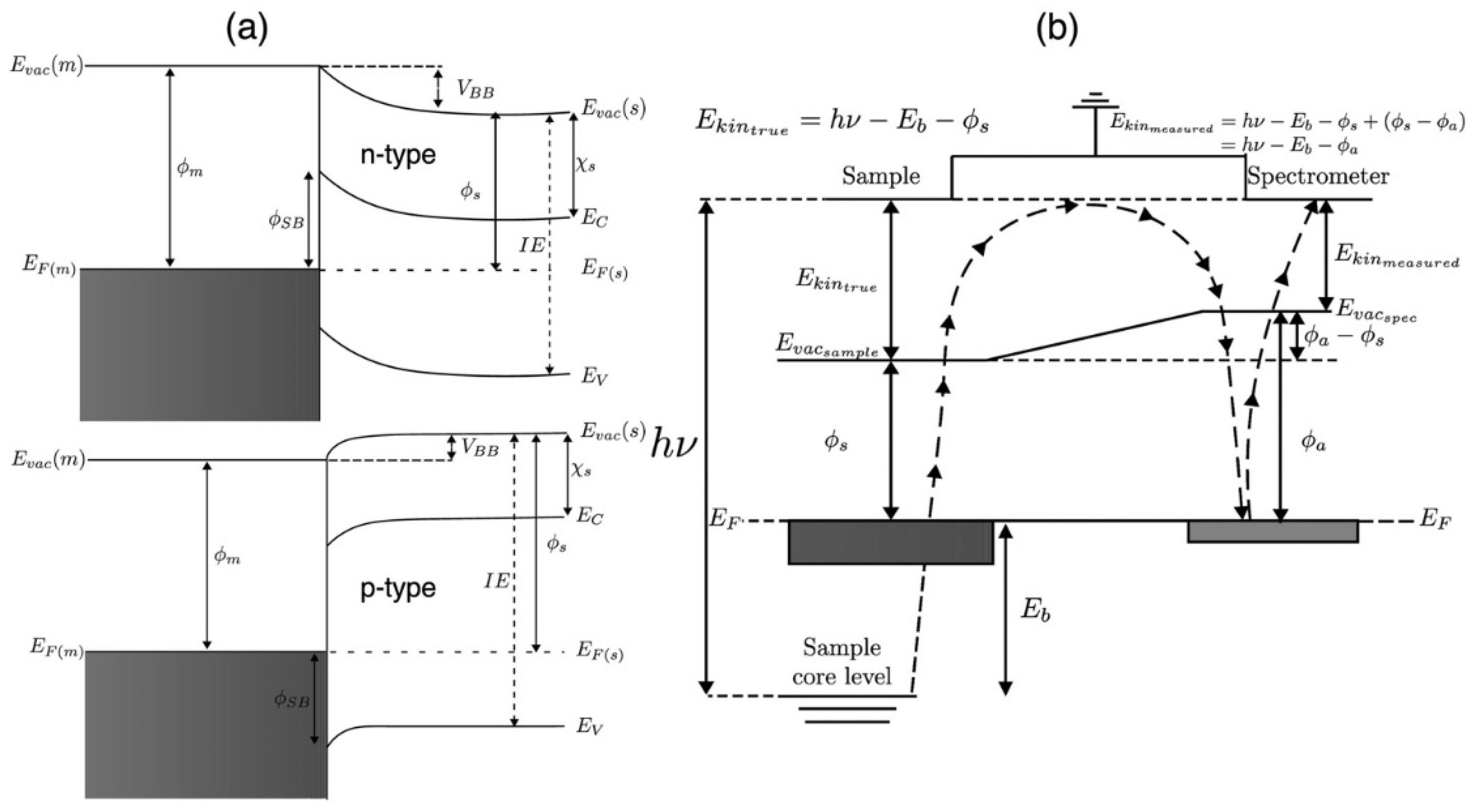
Owing to the global incentives targeted towards the advancement of semiconductor science and technology, the importance of a reliable method for the fundamental characterization of the interface between metals and low-dimensional semiconductors cannot be emphasized enough. For decades now, X-ray photoelectron spectroscopy (XPS) has been relied upon rather heavily when it comes down to investigating the band-bending, and hence the likelihood of a Schottky-barrier formation, at the resulting interfaces. However, the true extent to which the usually reported analyses of XPS measurements, attempting to unravel the true nature of metal–semiconductor interfaces, can be taken without a grain of salt is questionable at best. Therefore, in this article, a conceptual advance aiming to alter the status quo pertaining to the use of XPS for the aforementioned studies is presented.
Keywords:
Acknowledgments
References
- D. S. Schulman, A. J. Arnold, and Saptarshi Das, Contact Engineering for 2D Materials and Devices, Chem Soc Rev 47, 3037 (2018). [CrossRef]
- A. Dhingra, D. E. Nikonov, A. Lipatov, A. Sinitskii, and P. A. Dowben, What Happens When Transition Metal Trichalcogenides Are Interfaced with Gold?, J Mater Res 38, 52 (2023). [CrossRef]
- W. Schottky, Zur Halbleitertheorie Der Sperrschicht- Und Spitzengleichrichter, Zeitschrift Für Physik 113, 367 (1939). [CrossRef]
- N. F. Mott, The Theory of Crystal Rectifiers, Proceedings of the Royal Society A 171, 153 (1939). [CrossRef]
- A. Dhingra, A. Lipatov, M. J. Loes, J. Abourahma, M. Pink, A. Sinitskii, and P. A. Dowben, Effect of Au/HfS3 Interfacial Interactions on Properties of HfS3-Based Devices, Physical Chemistry Chemical Physics 24, 14016 (2022). [CrossRef]
- Z. Zhang and J. T. Yates, Band Bending in Semiconductors: Chemical and Physical Consequences at Surfaces and Interfaces, Chem Rev 112, 5520 (2012). [CrossRef]
- J. R. Waldrop and R. W. Grant, Interface Chemistry of Metal-GaAs Schottky-Barrier Contacts, Appl Phys Lett 34, 630 (1979). [CrossRef]
- S. Chen, S. Wang, C. Wang, Z. Wang, and Q. Liu, Latest Advance on Seamless Metal-Semiconductor Contact with Ultralow Schottky Barrier in 2D-Material-Based Devices, Nano Today 42, 101372 (2022). [CrossRef]
- Y. Gao, Surface Analytical Studies of Interfaces in Organic Semiconductor Devices, Materials Science and Engineering: R: Reports 68, 39 (2010). [CrossRef]
- K. Horn, Semiconductor Interface Studies Using Core and Valence Level Photoemission, Applied Physics A Solids and Surfaces 51, 289 (1990). [CrossRef]
- G. Viswan, K. Wang, R. Streubel, X. Hong, N. Valanoor, D. Sando, and P. A. Dowben, Magnetocapacitance at the Ni/BiInO3 Schottky Interface, ACS Appl Mater Interfaces 16, 4108 (2024). [CrossRef]
- N. Wu, Z. Xing, L. Luo, and G. Li, Normally-off GaON/p-GaN Gate HEMTs with Selective Plasma Oxidation: From Structural Characterization, Performance Improvement to Physical Mechanism, Semicond Sci Technol 39, 045015 (2024). [CrossRef]
- M.-Y. Kim, D.-W. Byun, G.-H. Lee, S. Pookpanratana, Q. Li, and S.-M. Koo, Schottky Barrier Heights and Electronic Transport in Ga2O3 Schottky Diodes, Mater Res Express 10, 075902 (2023). [CrossRef]
- A. Dhingra, A. Lipatov, A. Sinitskii, and P. A. Dowben, Complexities at the Au/ZrS3(001) Interface Probed by x-Ray Photoemission Spectroscopy, Journal of Physics: Condensed Matter 33, 434001 (2021). [CrossRef]
- S. J. Gilbert, A. Lipatov, A. J. Yost, M. J. Loes, A. Sinitskii, and P. A. Dowben, The Electronic Properties of Au and Pt Metal Contacts on Quasi-One-Dimensional Layered TiS3(001), Appl Phys Lett 114, 101604 (2019). [CrossRef]
- D. Caliskan, H. Sezen, E. Ozbay, and S. Suzer, Chemical Visualization of a GaN P-n Junction by XPS, Sci Rep 5, 14091 (2015). [CrossRef]
- S. Schuwalow et al., Band Structure Extraction at Hybrid Narrow-Gap Semiconductor–Metal Interfaces, Advanced Science 8, (2021). [CrossRef]
- A. Dhingra et al., Surface Termination and Schottky-Barrier Formation of In4Se3(001), Semicond Sci Technol 35, 065009 (2020). [CrossRef]
- L. A. M. Lyle, T. C. Back, C. T. Bowers, A. J. Green, K. D. Chabak, D. L. Dorsey, E. R. Heller, and L. M. Porter, Electrical and Chemical Analysis of Ti/Au Contacts to β -Ga2O3, APL Mater 9, 061104 (2021). [CrossRef]
- L. A. M. Lyle, Critical Review of Ohmic and Schottky Contacts to β-Ga2O3, Journal of Vacuum Science & Technology A 40, (2022). [CrossRef]
- R. T. Tung, The Physics and Chemistry of the Schottky Barrier Height, Appl Phys Rev 1, (2014). [CrossRef]
- Y. Liu, Q. Zhang, W. Zhang, R. Zhang, B. Wang, C. Ji, Z. Pei, and S. Sang, Tuning Schottky Barrier and Contact Type of Metal–Semiconductor in Ti3C2T2/MoS2 (T = F, O, OH) by Strain: A First-Principles Study, The Journal of Physical Chemistry C 125, 16200 (2021). [CrossRef]
- D. Wang, C. Tan, S. Wang, Z. Yang, L. Yang, and Z. Wang, Sm and Gd Contacts in 2D Semiconductors for High-Performance Electronics and Spintronics, ACS Appl Mater Interfaces 16, 14064 (2024). [CrossRef]
- T. Nishimura, K. Kita, and A. Toriumi, Evidence for Strong Fermi-Level Pinning Due to Metal-Induced Gap States at Metal/Germanium Interface, Appl Phys Lett 91, (2007). [CrossRef]
- S. Li, J. Chen, X. He, Y. Zheng, C. Yu, and H. Lu, Comparative Study of the Micro-Mechanism of Charge Redistribution at Metal-Semiconductor and Semimetal-Semiconductor Interfaces: Pt(Ni)-MoS2 and Bi-MoS2(WSe2) as the Prototype, Appl Surf Sci 623, 157036 (2023). [CrossRef]
- L.-X. Zhou et al., Quasi-Bonding-Induced Gap States in Metal/Two-Dimensional Semiconductor Junctions: Route for Schottky Barrier Height Reduction, Phys Rev B 105, 224105 (2022). [CrossRef]
- G. Greczynski and L. Hultman, A Step-by-Step Guide to Perform x-Ray Photoelectron Spectroscopy, J Appl Phys 132, (2022). [CrossRef]
- A. Dhingra, Physical and Electronic Properties of Two-Dimensional Layered Materials: In4Se3, TiS3, ZrS3, HfS3, and GeI2, University of Nebraska-Lincoln, 2022.
- G. Greczynski and L. Hultman, X-Ray Photoelectron Spectroscopy: Towards Reliable Binding Energy Referencing, Prog Mater Sci 107, 100591 (2020). [CrossRef]
- A. Dhingra, P. A. Dowben, A. Lipatov, and A. Sinitskii, HfS3 FIELD-EFFECT TRANSISTORS WITH A TWO-DIMENSIONAL HOLE GAS, US-20240162342-A1 (16 May 2024).
- S. J. Gilbert et al., Effect of Band Symmetry on Photocurrent Production in Quasi-One-Dimensional Transition-Metal Trichalcogenides, ACS Appl Mater Interfaces 12, 40525 (2020). [CrossRef]
- C. Cheng, J. He, and J. Hu, Naturally Asymmetrical Double-Schottky Barrier Model: Based on Observation of Bicrystal, Appl Phys Lett 101, (2012). [CrossRef]
- Q. Wang, C. Liu, B. Ma, Y. Gao, M. Fitzpatrick, Y. Li, B. Liu, C. Gao, and Y. Ma, High Pressure Study of B12As2: Electrical Transport Behavior and the Role of Grain Boundaries, J Appl Phys 117, (2015). [CrossRef]
- A. Grillo and A. Di Bartolomeo, A Current–Voltage Model for Double Schottky Barrier Devices, Adv Electron Mater 7, (2021). [CrossRef]
- Z. Cheng, Z. Hou, Y. Wang, M. Guo, K. Wu, J. Li, and Y. Lin, Steadily Decreasing Power Loss of a Double Schottky Barrier Originating from the Dynamics of Mobile Ions with Stable Interface States, Phys Rev Appl 17, 034042 (2022). [CrossRef]
- E. Echeverría, G. Peterson, B. Dong, S. Gilbert, A. Oyelade, M. Nastasi, J. A. Kelber, and P. A. Dowben, Band Bending at the Gold (Au)/Boron Carbide-Based Semiconductor Interface, Zeitschrift Für Physikalische Chemie 232, 893 (2018). [CrossRef]
Disclaimer/Publisher’s Note: The statements, opinions and data contained in all publications are solely those of the individual author(s) and contributor(s) and not of MDPI and/or the editor(s). MDPI and/or the editor(s) disclaim responsibility for any injury to people or property resulting from any ideas, methods, instructions or products referred to in the content. |
© 2025 by the authors. Licensee MDPI, Basel, Switzerland. This article is an open access article distributed under the terms and conditions of the Creative Commons Attribution (CC BY) license (http://creativecommons.org/licenses/by/4.0/).