Submitted:
08 February 2025
Posted:
10 February 2025
You are already at the latest version
Abstract
With the advancement of the semiconductor industry into the sub-10 nm regime, high-performance, low-energy transistors have become important, and gate-all-around junctionless field-effect transistors (GAA-JLFETs) have been developed to meet the demands. Silicon (Si) is still the dominant semiconductor material, but other potential alternatives like gallium arsenide (GaAs) provide much higher electron mobility, improving the drive current and switching speed. In this study, our contributions are a comparative analysis of Si and GaAs-based cylindrical GAA-JLFETs, using threshold voltage behavior, electrostatic control, short channel effects, subthreshold slope, drain-induced barrier lowering, and leakage current as the metrics in the evaluation of performance. A comprehensive analytical modeling approach is employed, solving Poisson's equation and utilizing numerical simulations to assess device characteristics using the ATLAS SILVACO tool under varying channel lengths and gate biases. Comparisons between Si and GaAs-based devices show what trade-offs exist and what the material engineering strategies are to use the advantages of GaAs and reduce some disadvantages. The results from the study are a valuable contribution to the design and optimization of next-generation FET architectures, pointing the direction for enabling next-generation beyond CMOS technology.
Keywords:
1. Introduction
2. Theoretical and Simulation Framework
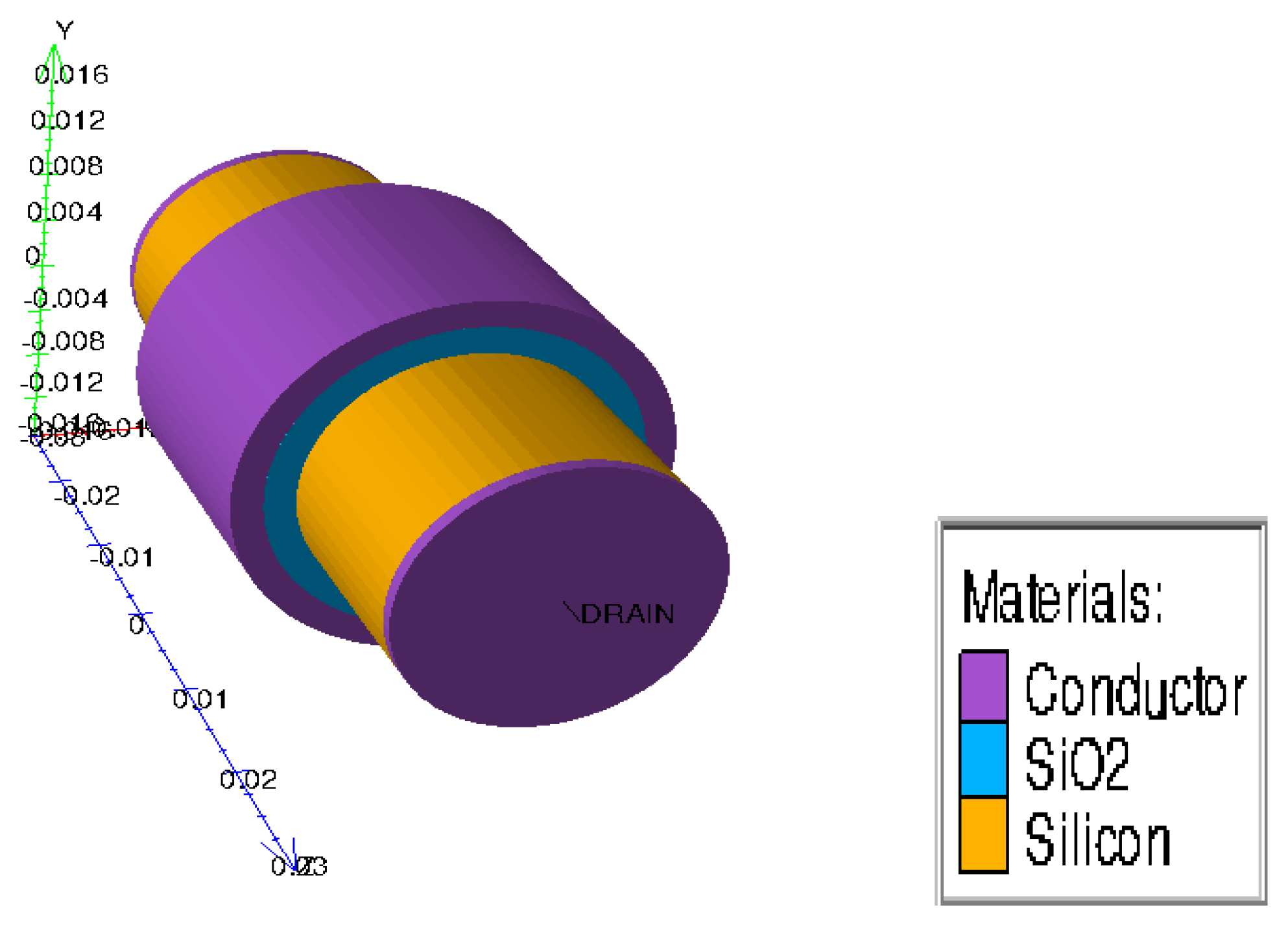
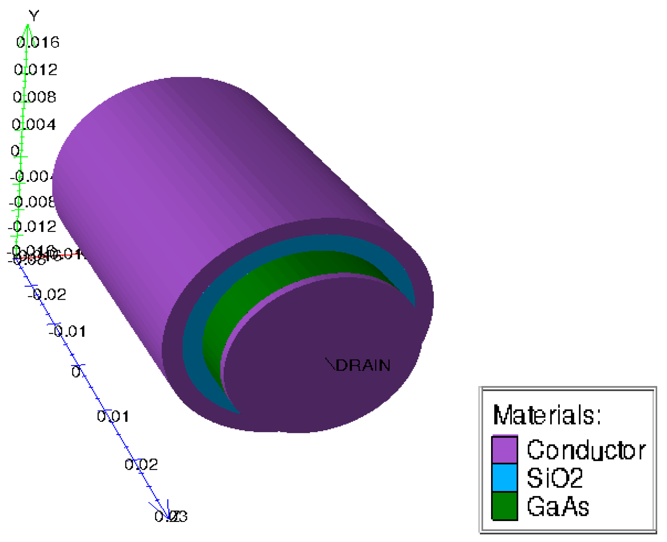
3. Methodology and Device Structure of JLFET
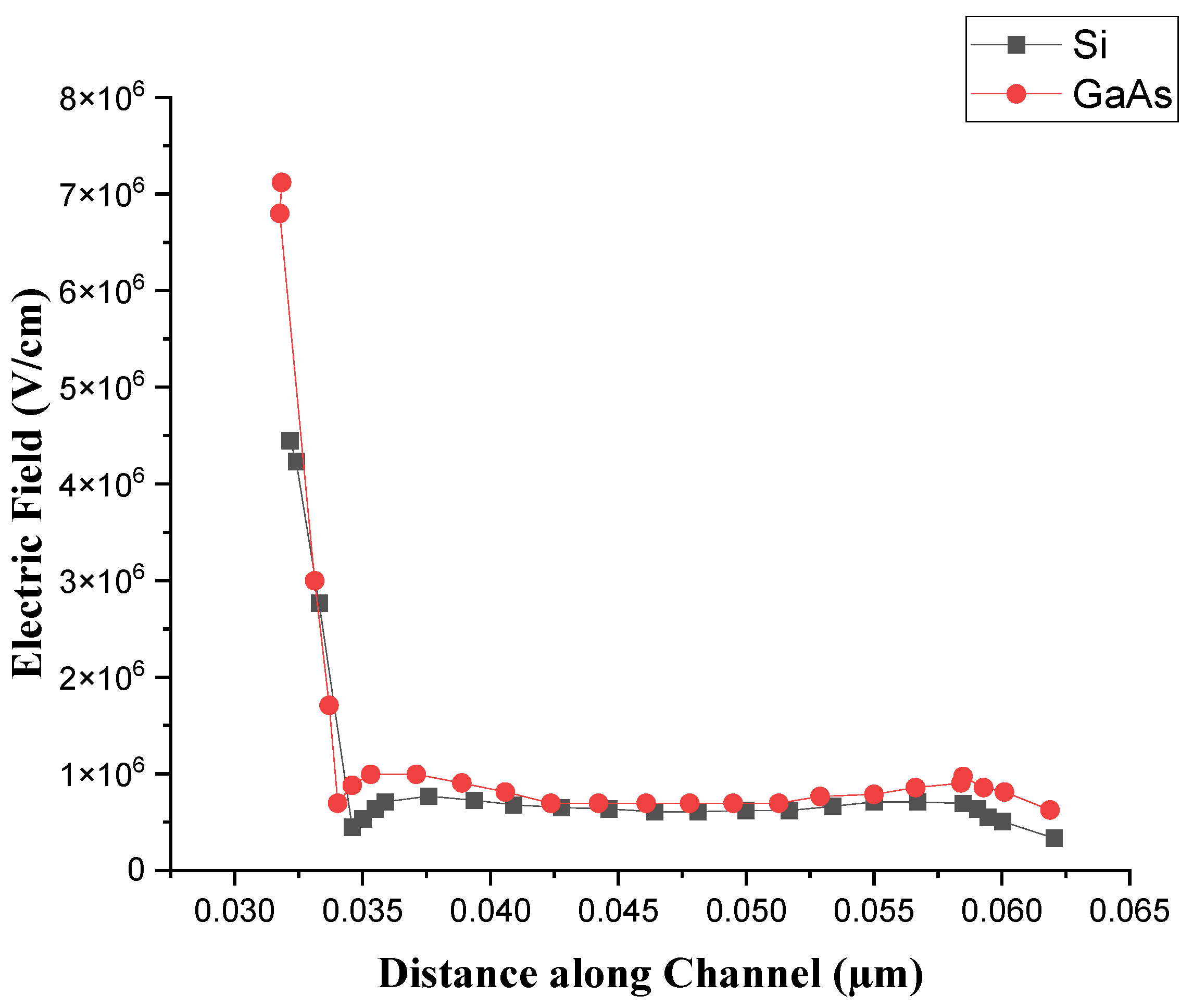
4. Result and Discussions
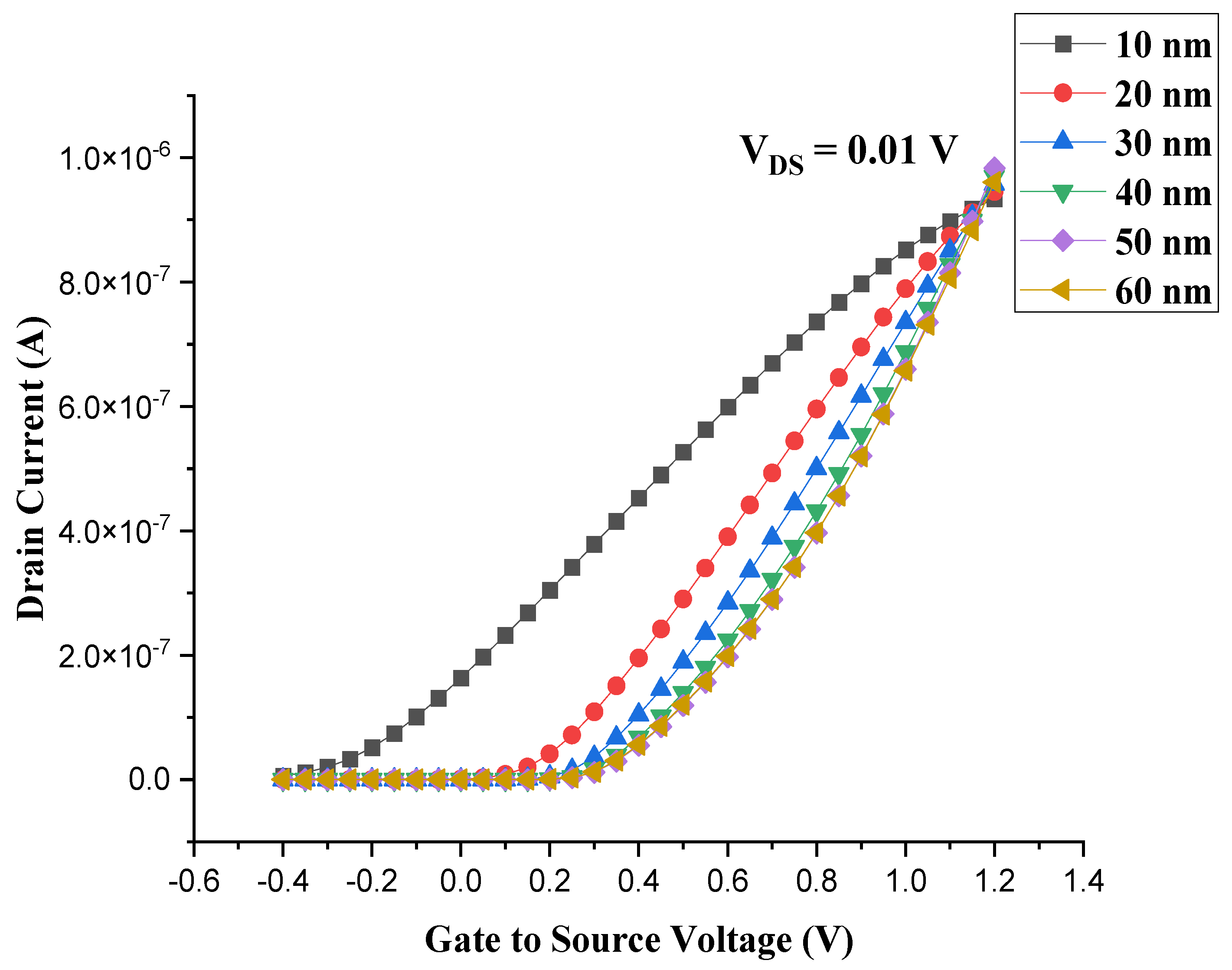
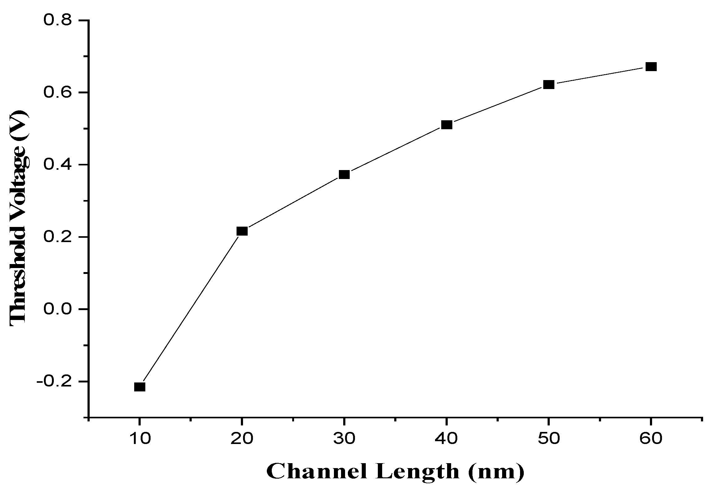
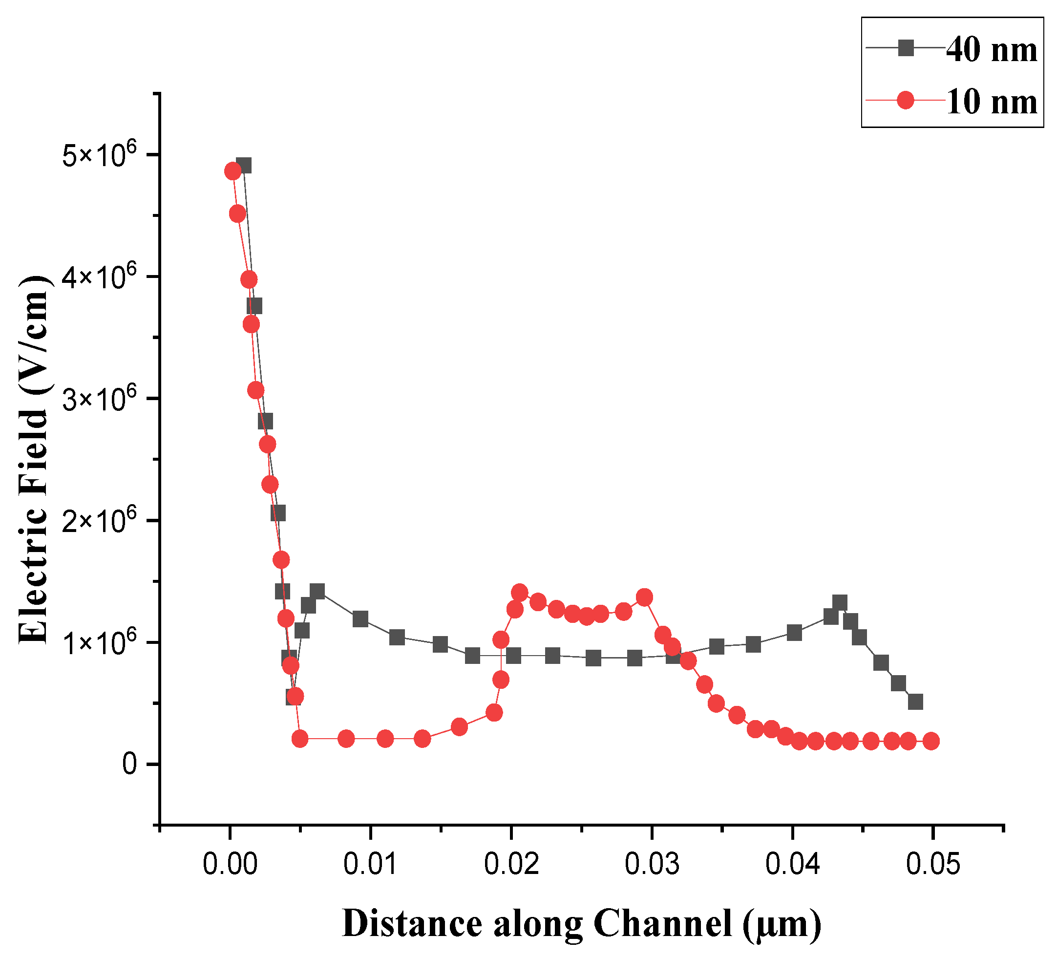
5. Comparative DC Analysis of Si-Based ` CGAA-JLFET with Different Channel Lengths
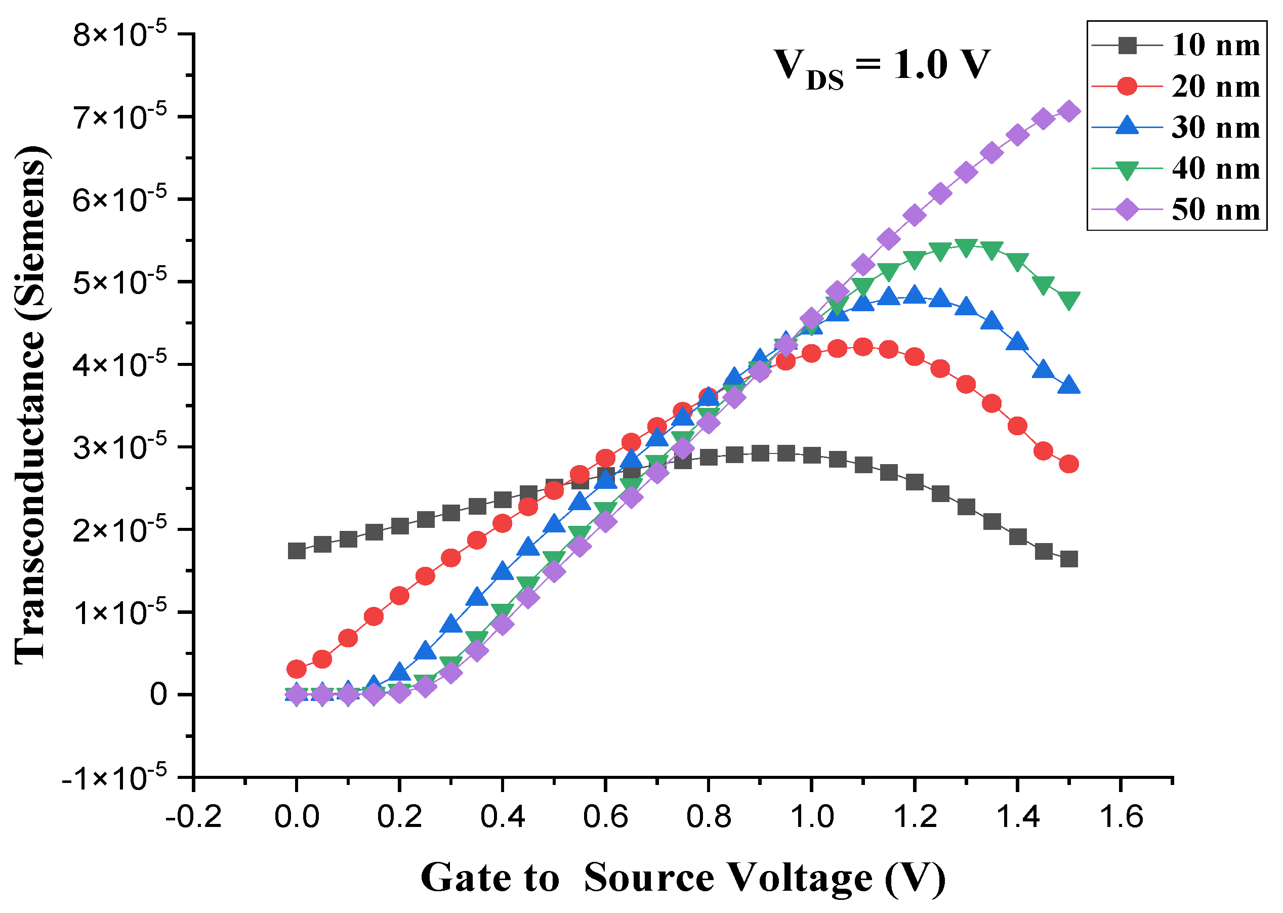
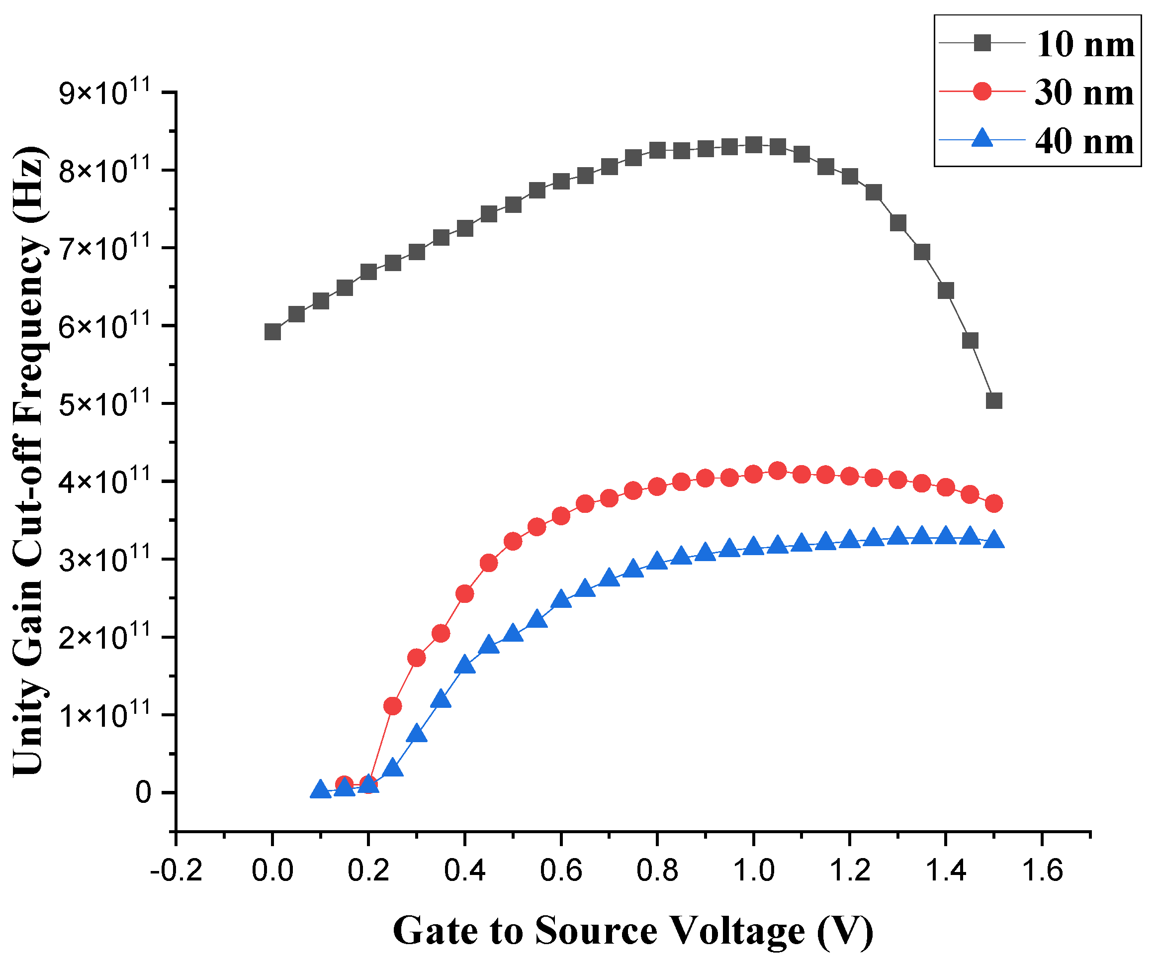
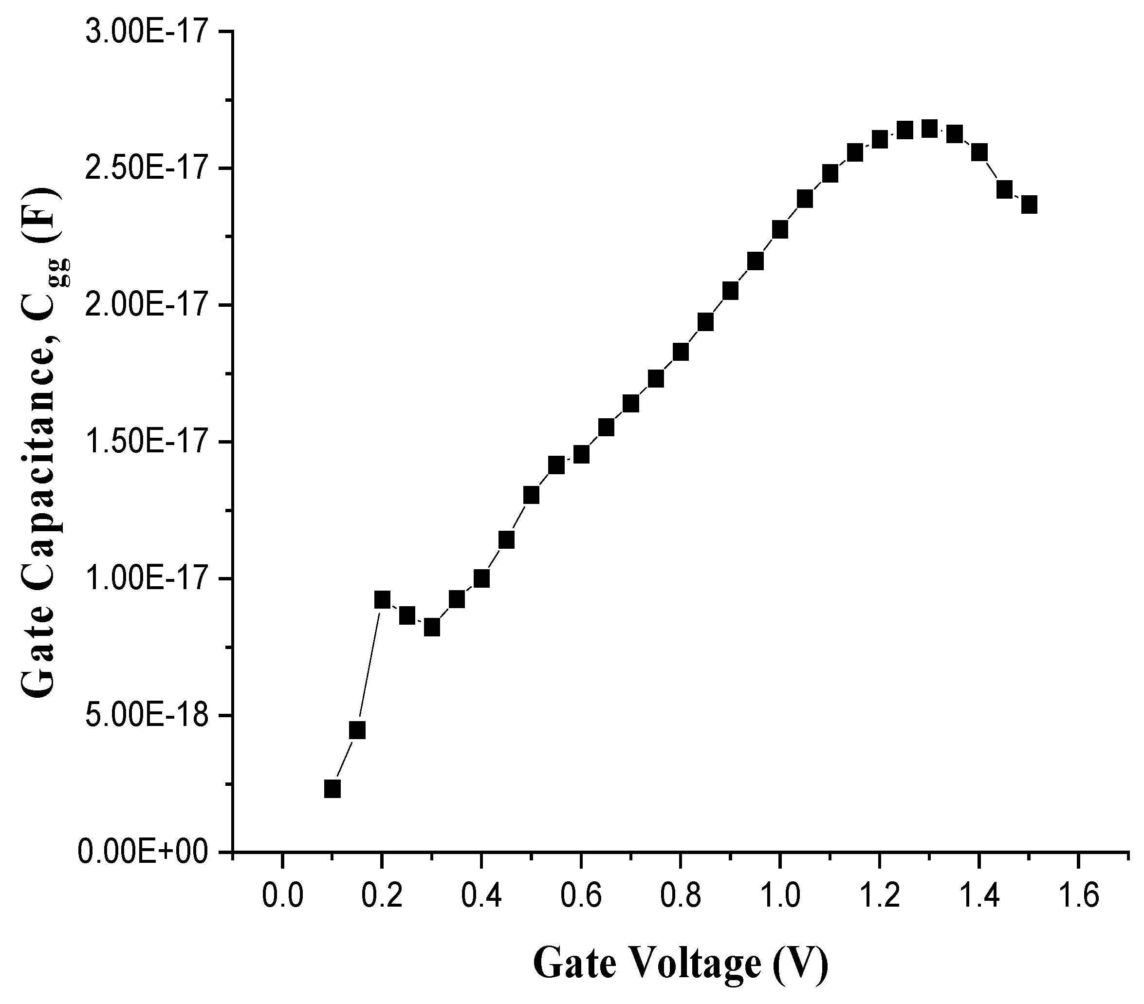
6. AC Analysis of Si-Based CGAA-JLFET with Different Channel Lengths
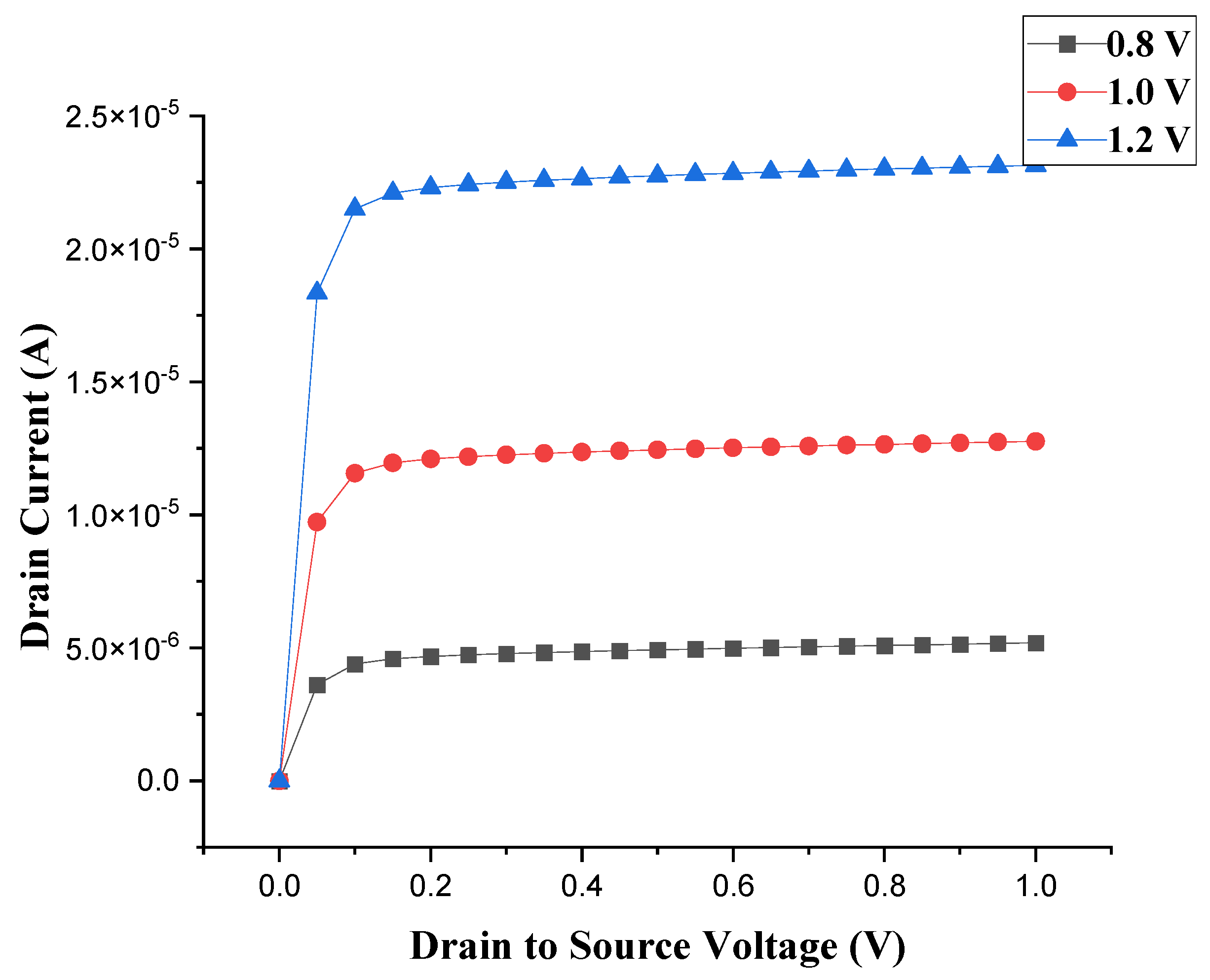
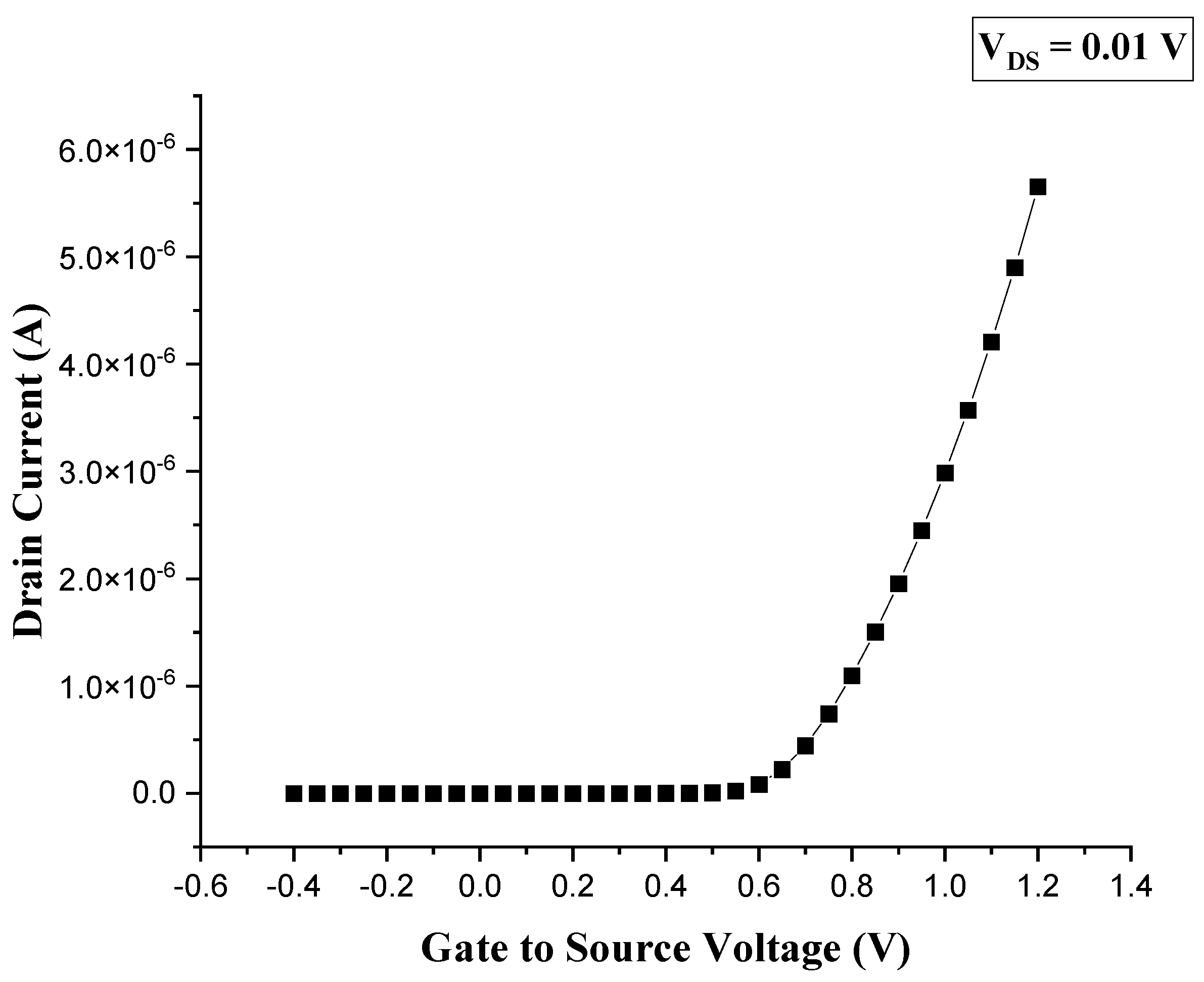
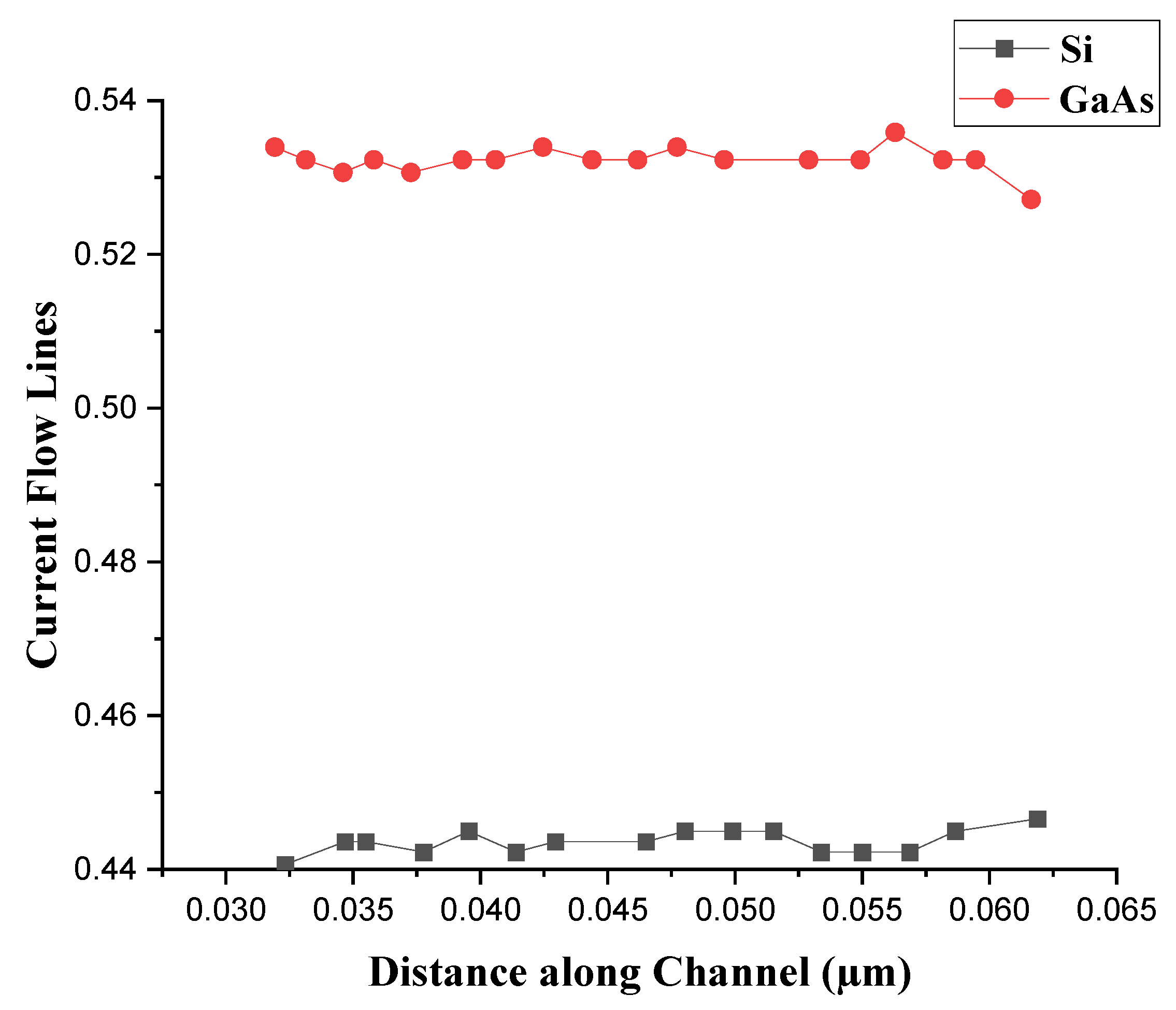
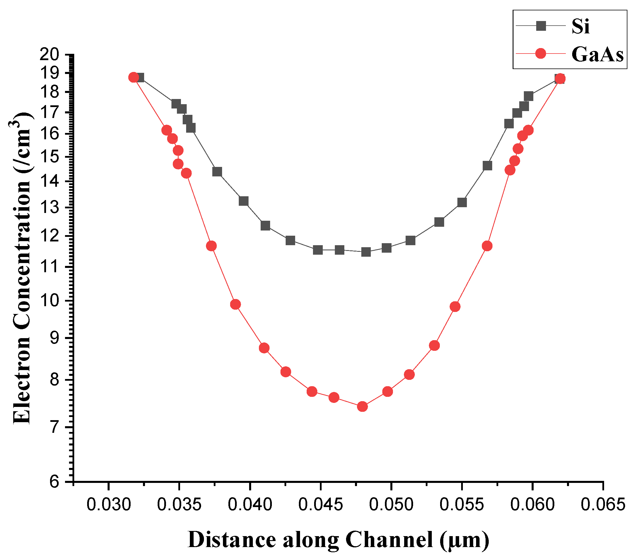
7. Simulated Results and Discussion for GaAs-Based JLFET
8. Conclusion
Author Contributions
Funding
Data Availability Statement
Acknowledgments
Conflicts of Interest
Abbreviations
| JLFET | Juncionless field effect transistor |
| SCEs | Short channel effects |
| DIBL | Drain-induced barrier lowering |
| SS | Subthreshold slope |
References
- Sze, S.; Ng, K. K. LEDs and lasers. Physics of semiconductor devices, 2006, vol. 3, pp. 601-657. [CrossRef]
- Jurczak, M.; Collaert, N.; Veloso, A.; Hoffmann, T; Biesemans, S. Review of FINFET technology. In IEEE international SOI conference, 2009, IEEE, pp. 1-4.
- Colinge, J. P. The junctionless transistor. In Emerging devices for low-power and high-performance nanosystems: Jenny Stanford Publishing, 2018, pp. 2-72.
- Theis, T. N.; Wong, H. S. P. The end of Moore's law: A new beginning for information technology. Computing in science & engineering, 2017, vol. 19, no. 2, pp. 41-50.
- Kumar, M. J.; Sahay, S. Junction-Less Field Effect Transistors: The First Transistor to be Conceptualized. 75th Anniversary of the transistor, pp. 51-63, 2023.
- Srivastava, S.; Acharya, A. Challenges and future scope of gate-all-around (GAA) transistors: Physical insights of device- circuit interactions. in Device Circuit Co-Design Issues in FETs: CRC Press, 2024, pp. 231-258.
- Baksh, S. S.; Sarin, R.; Amin, S. I.; Anand, S. Design of GaAs based Junctionless field effect transistor and its performance evaluation. Journal of Nanoelectronics and Optoelectronics, 2018, vol. 13, no. 1, pp. 32-37. [CrossRef]
- Frank, D. J.; Dennard, R. H.; Nowak, E.; Solomon, P. M.; Taur, Y.; Wong, H. S. P. Device scaling limits of Si MOSFETs and their application dependencies. Proceedings of the IEEE, vol. 89, no. 3, pp. 259-288, 2001. [CrossRef]
- Raut, P.; Nanda, U.; Panda, D. K. Recent trends on junction-less field effect transistors in terms of device topology, modeling, and application. ECS Journal of Solid State Science and Technology, 2023, vol. 12, no. 3, p. 031010. [CrossRef]
- Hossain, N. M.; Quader, S.; Siddik, A. B.; Chowdhury, M. I. B. TCAD based performance analysis of junctionless cylindrical double gate all around FET up to 5nm technology node. In 2017 20th International Conference of Computer and Information Technology (ICCIT), 2017: IEEE, pp. 1-4.
- Ghosh, S.; Jana, A.; Agnihotri, A. K.; Kundu, S.; Das, D.; Sarkar, S. K. DC and analog/RF performance comparison of renovated GAA JLFET structures. in 2022 IEEE VLSI Device Circuit and System (VLSI DCS), 2022: IEEE, pp. 80-84.
- Srivastava, P.; Upadhyaya, A.; Yadav, S.; Negi, C. Performance Evaluation of Junctionless Cylindrical Gate-All-Around FET for Low Power Applications. Semiconductor Science and Information Devices, 2023, vol. 5, no. 2, pp. 1-10,. [CrossRef]
- Kumari, A.; Saini, A.; Kumar, A.; Kumar, V.; Kumar, M. Recent Developments and Challenges in Strained Junctionless MOSFETs: A Review. in 2023 International Conference on Computational Intelligence and Sustainable Engineering Solutions (CISES), 2023: IEEE, pp. 118-122.
- Dixit, V. K.; Gupta, R.; Srinivas, P.; Dubey, S. Back Bias Induced Modeling of Subthreshold Characteristics of SOI Junctionless Field Effect Transistor (JLFET). Silicon, 2021. vol. 13, pp. 1961-1967. [CrossRef]
- DEHZANGI, A. FABRICATION AND SIMULATION OF P-TYPE JUNCTIONLESS SILICON NANO-WIRE TRANSISTOR ON SILICON ON INSULATOR BY AFM NANO LITHOGRAPHY. School of Graduate Studies, Universiti Putra Malaysia, 2012.
- Scognamiglio, L. 3D Junctionless-FET technology: A comparative TCAD simulation study with FinFET and NSGAAFET. Politecnico di Torino, 2022.
- Chuan, M. W. et al. A review of the top of the barrier nanotransistor models for semiconductor nanomaterials. Superlattices and Microstructures, 2020, vol. 140, p. 106429. [CrossRef]
- Xie, Q.; Xu, J.; Taur, Y. Review and critique of analytic models of MOSFET short-channel effects in subthreshold. IEEE transactions on electron devices, 2012, vol. 59, no. 6, pp. 1569-1579. [CrossRef]
- Rao, R.; Srivastava, A.; Blaauw, D.; Sylvester, D. Statistical analysis of subthreshold leakage current for VLSI circuits. IEEE Transactions on Very Large Scale Integration (VLSI) Systems, 2004, vol. 12, no. 2, pp. 131-139. [CrossRef]
- Querlioz, D. et al. On the ability of the particle Monte Carlo technique to include quantum effects in nano-MOSFET simulation. IEEE transactions on electron devices, 2007, vol. 54, no. 9, pp. 2232-2242. [CrossRef]
- Colinge, J. P. et al. Nano-wire transistors without junctions. Nature nanotechnology, 2010, vol. 5, no. 3, pp. 225-229.
- Misra, S.; Biswal, S. M.; Bara, B.; Swain, S. K.; Pati, S. K. Study of effect of downscaling on the analog/RF performance of gate all around JLMOSFET. in 2018 IEEE Electron Devices Kolkata Conference (EDKCON), 2018: IEEE, pp. 234-241.
- Chen, L.C. et al. The physical analysis on electrical junction of junctionless FET. AIP Advances, 2017, vol. 7, no. 2. [CrossRef]
- Singh, B.; Gola, D.; Singh, K.; Goel, E.; Kumar, S.; Jit, S. Analytical modeling of subthreshold characteristics of ion-implanted symmetric double gate junctionless field effect transistors. Materials science in semiconductor processing, 2017, vol. 58, pp. 82-88. [CrossRef]
- Meriga, C.; Ponnuri, R. T.; Krishna, B. V.; Saidulu, S. A.; Prakesh, M. D. Dual gate junctionless gate-all-around (JL-GAA) FETs using hybrid structured channels. In 2020 International Conference for Emerging Technology (INCET), 2020: IEEE, pp. 1-4.
- Pandey, S.; Sahu, C.; Singh, J. A highly linear RF mixer using gate-all-around junctionless transistor. International Journal of Electronics Letters, 2017, vol. 5, no. 2, pp. 129-136.
- Singh, B. Analytical Modeling and Simulation of Double Gate Junctionless Field Effect Transistors (DG-JLFETs). 2017.
- Hossain, S.; Iqbal, M. A.; Samant, P.; Siddiki, M. K.; Rahman, M. More Than a Device: Function Implementation in a Multi-Gate Junctionless FET Structure. Journal of Electronics and Electrical Engineering, 2023, pp. 1–11-1–11.
- Pavanello, M. A.; Martino, J. A. A.; Simoen, E.; Rooyackers, R.; Collaert, N.; Claeys, C. Temperature influences on FinFETs with undoped body. ECS Transactions, 2007, vol. 6, no. 4, p. 211. [CrossRef]
- Nazarov, A.; Balestra, F.; Kilchytska, V.; Flandre, D. Functional nanomaterials and devices for electronics, sensors and energy harvesting. Springer, 2014.
- Yadav S.; Negi, C. M. S. Novel L-shaped drain dual-gate SiGe MOSFET for high-frequency, low power applications. International Journal of Numerical Modelling: Electronic Networks, Devices and Fields, 2023, vol. 36, no. 1, p. e3039.
- Kamath, A. et al. Junctionless CMOS transistors with independent doublegates. International Journal of Information and Electronics Engineering, 2013, vol. 3, no. 1, p. 13.
- Rewari, S.; Nath, V.; Haldar, S.; Deswal, S.; Gupta, R. AC analysis of Junctionless Double Surrounding Gate (JLDSG) MOSFET for Tera Hertz applications. in 2016 International Conference on Computational Techniques in Information and Communication Technologies (ICCTICT), 2016: IEEE, pp. 113-117.
- Joshi, R. K.; Arjun, T.; Ahish, S.; Sharma, D.; Vasantha, M.; Kumar, Y. Implementation of double-gate junctionless transistor and its circuit performance analysis. In 2016 IEEE Students' Technology Symposium (TechSym), 2016: IEEE, pp. 278-283.
- Sahu C.; Singh, J. Device and circuit performance analysis of double gate junctionless transistors at L g= 18 nm. The Journal of Engineering, 2014, vol. 2014, no. 3, pp. 105-110.
- Yarlagadda, N.; Verma, Y. K.; Amarnath, G. A temperature dependent drain current model of P+ SiC GAA JLFETs for enhanced analog/RF performance. Micro and Nanostructures, 2024, vol. 188, p. 207786. [CrossRef]
- Dharmender; Nigam, K.; Kumar, S. Performance assessment of cavity on source dual material split gate GaAs/InAs/Ge junctionless TFET for label-free detection of biomolecules. Applied Physics A, 2022, vol. 128, no. 10, p. 943.
- CONGER, J.; PECZALSKI, A.; SHUR, M. S. Temperature modeling of GaAs DCFL. International Journal of High Speed Electronics and Systems, 1992, vol. 3, no. 02, pp. 171-199.
- Zhang, C.; Li, X. III–V nano-wire transistors for low-power logic applications: a review and outlook. IEEE Transactions on Electron Devices, 2015, vol. 63, no. 1, pp. 223-234.
- Nowbahari, A.; Roy, A.; Marchetti, L. Junctionless transistors: State-of-the-art. Electronics, 2020, vol. 9, no. 7, p. 1174. [CrossRef]

| Bias | Drain Current |
|---|---|
| Symbol | Value |
|---|---|
| DIBL coefficient | |
| Channel Perimeter | |
| When the surface is accumulated. | |
| The effective length of the neutral bulk channel | |
| The effective length of the accumulation channel | |
| Accumulation mobilities | |
| Bulk mobilities |
| Parameters | For Cylindrical Gate-All-Around JLFET |
|---|---|
| Channel Material | Silicon |
| Channel region with Doping Concentration | N-type – 1019 cm-3 |
| Source region with Doping Concentration | N-type – 1019 cm-3 |
| Drain region with Doping Concentration | N-type – 1019 cm-3 |
| Gate material | P+ Polysilicon |
| Gate Workfunction | 5.4 eV |
| Oxide Permittivity | 3.9 |
| Channel Length | Ranges 10 nm to 60 nm |
| Oxide Thickness | 2 nm (radius) |
| Semiconductor (Si-Substrate) Thickness | 10 nm (radius) |
| Device Length | 60 nm |
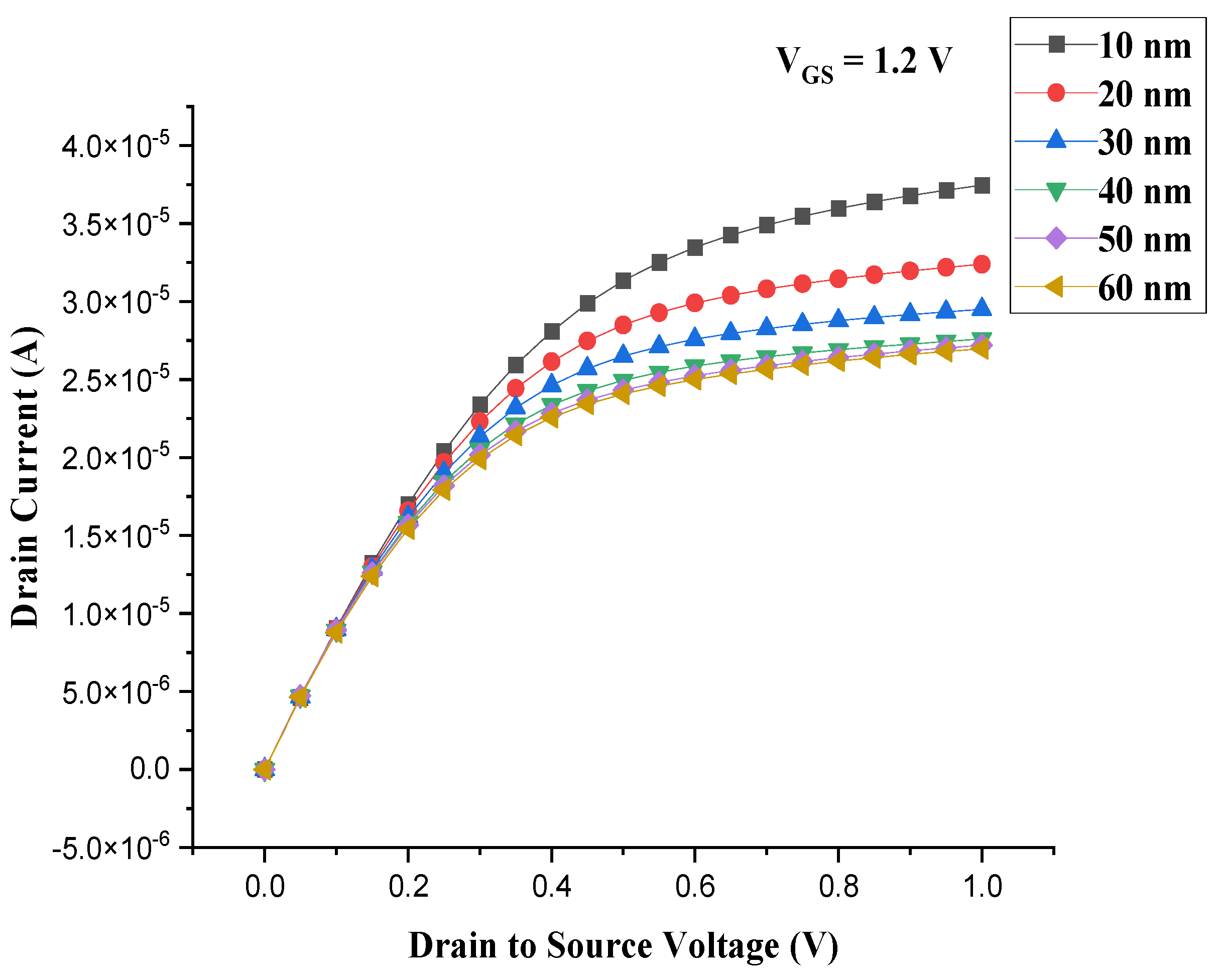
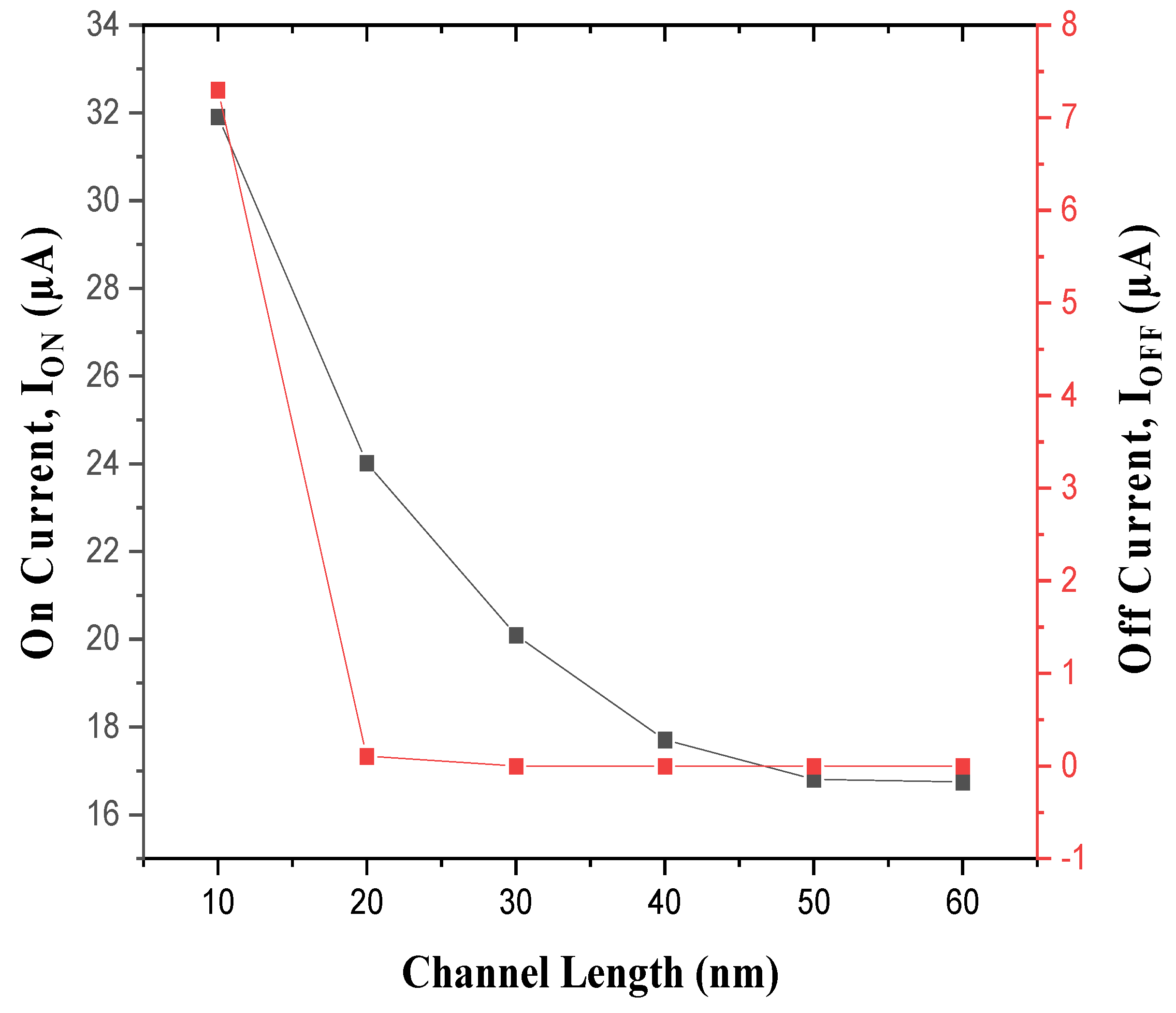
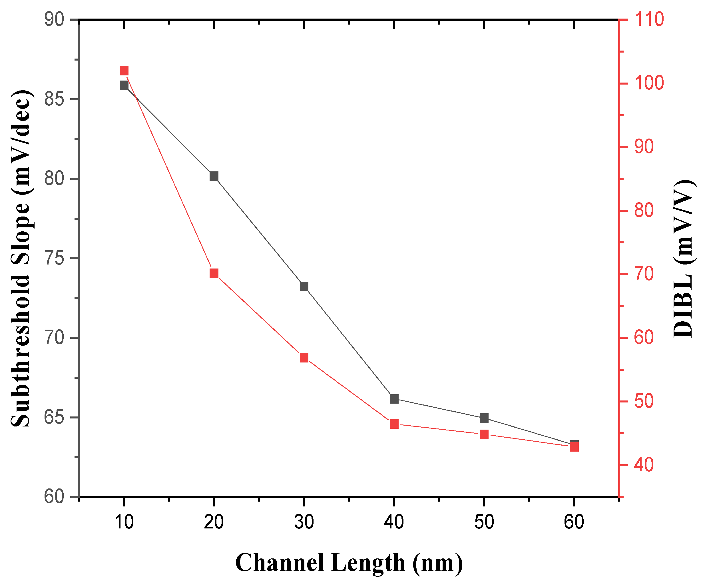
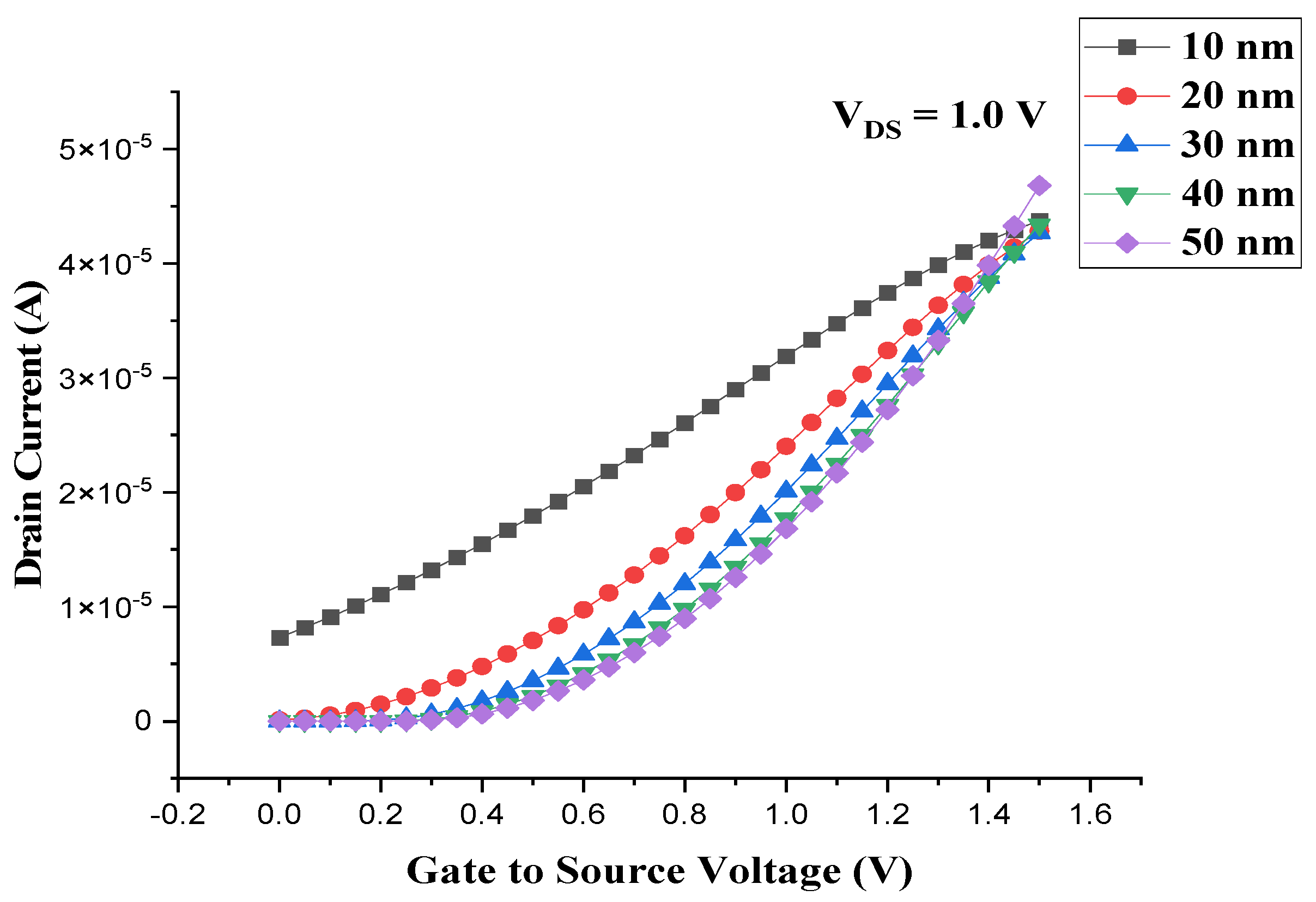
| Lg (nm) | Vth (V) | Saturation Slope (A) | Max. Drain Current (A) | SS (mV/dec) | DIBL (mV/V) | Ion (µA) | Ioff (µA) | Ion/Ioff |
|---|---|---|---|---|---|---|---|---|
| 10 | -0.21461 | 6.43265×10⁻⁶ | 3.74606 × 10⁻⁵ | 85.882 | 120 | 31.91620 | 7.30376 | 4.36983 |
| 20 | 0.216574 | 4.07531 × 10⁻⁶ | 3.23924 × 10⁻⁵ | 80.164 | 70.1652 | 24.0208 | 0.107591 | 223.2615 |
| 30 | 0.37356 | 3.1868 × 10⁻⁶ | 2.95 × 10⁻⁵ | 73.25 | 56.9015 | 20.0967 | 3.05421 × 10⁻⁴ | 6.5800 × 10⁴ |
| 40 | 0.511143 | 3.15754 × 10⁻⁶ | 2.76015 × 10⁻⁵ | 66.1718 | 46.4723 | 17.7135 | 1.31798 × 10⁻⁵ | 1.343985× 10⁶ |
| 50 | 0.622054 | 3.10029 × 10⁻⁶ | 2.720923 × 10⁻⁵ | 64.9612 | 44.8533 | 16.8105 | 4.95607 × 10⁻⁶ | 3.391905× 10⁶ |
| 60 | 0.671832 | 3.05913 × 10⁻⁶ | 2.698054 × 10⁻⁵ | 63.2760 | 42.8955 | 16.7533 | 3.9426 ×10⁻⁶ | 4.249305× 10⁶ |
| Device Architectures |
Authors | Lg (nm) | SS (mV/dec) | DIBL (mV/V) | Ion (µA) | Ioff (µA) | Ion/Ioff |
|---|---|---|---|---|---|---|---|
| Cylindrical Gate-all-around JLFET (This work) | P. Srivastava et al. | 60 | 63.2760 | 42.8955 | 16.7533 | 3.9426 ×10⁻⁶ | 4.249305× 10⁶ |
| FinFET | M. A. Pavanello et al. [29] | 60 | 85.41 | 120 | - | - | 1.61×10⁷ |
| UTBB MOS43 | F. Gamiz et al. [30] | 60 | 90 | 130 | - | - | - |
| LDMOS | S. Yadav et al. [31] | 60 | 70.061 | 116.853 | - | - | - |
| SDMOS | S. Yadav et al. [31] | 60 | 70.811 | 119.609 | - | - | - |
| Cylindrical Gate-all-around JLFET (This work) | P. Srivastava et al. | 40 | 66.1718 | 46.4723 | 17.7135 | 1.31798 × 10⁻⁵ | 1.343985× 10⁶ |
| JL FinFET PMOS | Kamath et al. [32] | 40 | 90 | - | 15.4 | - | 105 |
| JL FinFET NMOS | Kamath et al. [32] | 40 | 92 | - | 52.3 | - | 107 |
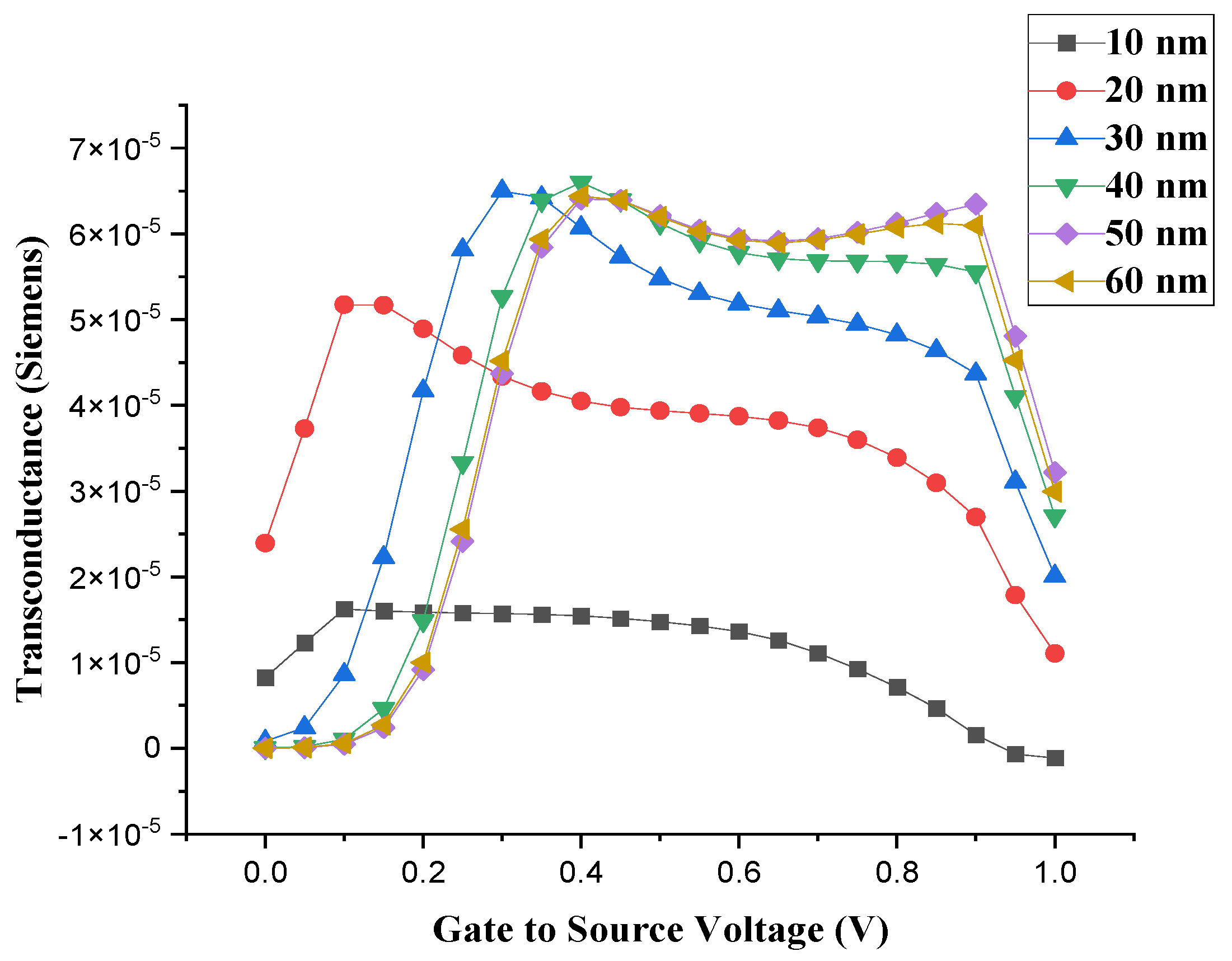
| Lg (nm) | Max. Drain Current (A) | Max. Transconductance (Siemens) | Max Oscillation Frequency (GHz) |
|---|---|---|---|
| 10 | 4.37285 × 10⁻⁵ | 2.92304× 10⁻⁵ | 1969.02945 |
| 20 | 4.28113 × 10⁻⁵ | 4.20951 × 10⁻⁵ | 1460.14232 |
| 30 | 4.2689 × 10⁻⁵ | 4.8144 × 10⁻⁵ | 1044.51938 |
| 40 | 4.23783 × 10⁻⁵ | 5.43787 × 10⁻⁵ | 761.921066 |
| 50 | 4.20062 × 10⁻⁵ | 7.06235 × 10⁻⁵ | 477.220384 |
| Parameters | GaAs-based CGAA-JLFET |
|---|---|
| Channel Material | Gallium Arsenide (GaAs) |
| Mesh-Length, Angle, Radius | In m |
| Region | Semiconductor, Silicon Oxide, Conductor for Source, Channel and Gate |
| Channel region with Doping Concentration | N-type – I019 cm-3 |
| Source region with Doping Concentration | N-type – I019 cm-3 |
| Drain region with Doping Concentration | N-type – I019 cm-3 |
| Gate material | P+ Polysilicon |
| Gate Workfunction | 5.4 eV |
| Oxide Permittivity | 3.9 |
| Channel Length | 40 nm |
| Oxide Thickness | 2 nm (radius) |
| Semiconductor (Si-Substrate) Thickness | 10 nm (radius) |
| Device Length | 60 nm |
| Property | Value for GaAs | Comparison with Silicon |
| Electron Mobility | 8500 cm²/V·s | Higher than silicon, enabling high-speed devices |
| Band Gap | 1.42 eV (Direct Band Gap) | Efficient for optoelectronics such as LEDs and laser diodes |
| Saturation Velocity | 1 × 10⁷ cm/s | Higher than silicon, it contributes to faster switching speeds |
| Breakdown Voltage | Higher than Silicon | Suitable for high-power and high-voltage applications |
| Crystal Structure | Zinc-blende | Similar to diamond, but with Ga and As in tetrahedral configuration |
| Lattice Constant | 5.653 Å | It affects material properties and device performance |
| Thermal Conductivity | 46 W/m·K | Lower than silicon, which can be a disadvantage in high-power applications |
| Thermal Expansion | 5.8 × 10⁻⁶ /°C | Different from silicon, which may cause thermal stress |
| Young's Modulus | 85-90 GPa | Relatively lower than silicon, making it more flexible |
| Hardness | Higher than Silicon | It makes GaAs more durable and resistant to scratching |
| Photoluminescence | Excellent | Used in optoelectronics such as LEDs and laser diodes |
| Absorption Spectrum | High in infrared | Useful for solar cells and photodetectors in the infrared range |
| Applications | High-frequency devices, optoelectronics, power electronics | Widely used in communications, high-speed electronics, and photonics |
| Cost | Higher than Silicon | Manufacturing GaAs is more expensive than silicon |
| Si and III-V Material | Vth (V) | Saturation Slope (A) | Max. Drain Current (A) | SS (mV/dec) | DIBL (mV/V) |
Ion (µA) | Ioff (µA) | Ion/Ioff |
|---|---|---|---|---|---|---|---|---|
| GaAs | 0.819608 | 6.41239 ×10⁻⁷ | 2.31345 ×10⁻⁵ |
64.47608 | 30.5962 | 12.7614 | 1.125467 ×10⁻⁹ |
1.133861 ×10¹⁰ |
| Si | 0.511143 | 3.15754 × 10⁻⁶ | 2.76015 × 10⁻⁵ | 66.1718 | 46.4723 | 17.7135 | 1.31798 × 10⁻⁵ | 1.343985× 10⁶ |
Disclaimer/Publisher’s Note: The statements, opinions and data contained in all publications are solely those of the individual author(s) and contributor(s) and not of MDPI and/or the editor(s). MDPI and/or the editor(s) disclaim responsibility for any injury to people or property resulting from any ideas, methods, instructions or products referred to in the content. |
© 2025 by the authors. Licensee MDPI, Basel, Switzerland. This article is an open access article distributed under the terms and conditions of the Creative Commons Attribution (CC BY) license (http://creativecommons.org/licenses/by/4.0/).


