
Submitted:
14 January 2025
Posted:
15 January 2025
You are already at the latest version
Abstract
This paper presents the design of a high-isolation directional coupler for X-band applications, utilizing substrate integrated waveguide (SIW) technology. The coupler features a simple structure, compact size, and ease of integration with other planar circuits. Typically, the S-parameters of a directional coupler are determined by the dimensions of the SIW and the aperture (or hole) of the coupler. In this study, we introduce additional via lines to modify the SIW and the coupler aperture, aiming to achieve high isolation. First, two via lines are embedded in the center, converging into two central vias that form the coupler's aperture. The power ratio within the coupler is controlled by adjusting the width of the aperture and the overall width of the SIW. Specifically, the width of the SIW at the aperture position is affected by adding vias on the two outer sides of the SIW. By incorporating these vias, we can effectively manage the power distribution across the four ports while ensuring sufficient isolation among them. The proposed design achieves an insertion loss of 3.3 dB, a coupling factor of 6 dB, and an isolation factor of 28.6 dB at 10 GHz. Experimental results demonstrate that the coupler maintains S_41 less than -20 dB over a 30% fractional bandwidth, ranging from 8.6 GHz to 11.6 GHz.
Keywords:
directional coupler
; substrate integrated waveguide
; X-band
; isolation
1. Introduction
A directional coupler is a passive microwave component used for power division. This device has four ports. In the coupler, the incident power at port 1 is transmitted to port 2 (the through port) and to port 3 (the coupled port), but not to port 4 (the isolated port) [1]. Directional couplers are commonly utilized in applications such as radar, satellite communication, point-to-point radio, and antenna beam-forming networks [2,3].
Traditionally, directional couplers are implemented in rectangular waveguides because they provide low insertion loss and high quality factors. However, rectangular waveguides can be costly, bulky, and challenging to integrate with printed structures. To address these issues, a new technique called substrate integrated waveguide (SIW) has been introduced. SIW combines aspects of microstrip and waveguide technologies.
An SIW consists of two metal layers with a substrate sandwiched in between and metallic vias connecting the two ground planes of the substrate. It offers several significant advantages, including low loss, high Q-factor, cost-effectiveness, and ease of integration with other planar devices [4,5]. Recently, many circuits have been designed using the SIW structure, including filters, couplers, power dividers, and antennas [6,7,8,9,10,11,12,13,14,15,16,17,18,19,20].
Directional couplers have been proposed for implementation in substrate-integrated waveguide (SIW) structures in several studies [2,3,6,9,10,11]. In [2] and [9,10,11], directional couplers are designed using a single-aperture (hole) structure. In this configuration, coupling is achieved through two narrow apertures located on the common broadside wall of two adjacent SIWs. The power distribution across the four ports of the coupler can be controlled by adjusting the width of the apertures. This design features a simple configuration and compact size.
In [12,13,14,15], couplers with multiple apertures are introduced. These designs offer a wider and flatter bandwidth; however, the increased number of apertures results in a larger overall coupler size. Meanwhile, in [16,17], the authors propose a method for adjusting the width of the SIW to control the S-parameters of the coupler. This approach can improve the performance of the S-parameters significantly.
In this paper, we introduce the addition of metallic vias to enhance the isolation factor of the coupler. These vias are used to separate the electromagnetic fields of adjacent substrate integrated waveguides (SIWs) and also play a role in controlling the S-parameters of the coupler by allowing for adjustments in the width of the SIW. Simulation and experimental results indicate that the proposed coupler can achieve a 30% fractional bandwidth with isolation factor smaller than -20 dB.
The paper is organized as follows: Section II presents the theoretical considerations of SIWs and SIW directional couplers. Section III details the design concept of the pro-posed X-band directional coupler. The experimental results of the two configurations are discussed in Section IV. Section V provides a comparison and discussion of the findings. Finally, Section VI concludes the paper.
2. Theory of SIW and a SIW Directional Coupler
2.1. Substrate Integrated Waveguide
The structure of the substrate integrated waveguide (SIW) transmission line is depicted in Figure 1a [4]. The SIW transmission line comprises a top metal layer, a ground layer, and a middle substrate layer. There are two rows of metallic vias along the line that facilitate the transmission of signals within them. The SIW line supports TE10 mode exclusively at the operating frequency indicated in Figure 1b.
The essential design parameters of a Substrate Integrated Waveguide (SIW) transmission line are shown in Figure 2. In the figure, w and l represent the width and length of the SIW, respectively. The parameters for the vias are d and p, which denote the diameter of the via and the distance between two adjacent vias. It is important for the values of d and p to satisfy Equations 1, 2, and 3 in order to minimize loss.
where is guiding wavelength in SIW
where c, are speed of light and frequency, respectively.
2.2. SIW Directional Coupler
A basic structure of a four-port directional coupler is illustrated in Figure 3. This coupler is used to divide and distribute power. An incident signal enters through Input Port 1, where most of its power is transmitted to Transmitted Port 2. Power is also coupled to Coupled Port 3 from the input signal at Port 1. Finally, Port 4 is an isolated port, which does not receive any power from the input.
The fundamental parameters of directional coupler are listed below:
Coupling:
Insertion loss:
Isolation:
Directivity
The simple SIW directional coupler features a single-aperture design [2]. Figure 4 illustrates the single-aperture SIW coupler. In this type of coupler, the critical parameter is the width of the aperture, as it influences the power distribution between the output ports. Tappers are used to connect transmission lines to the SIW. By incorporating tappers, the bandwidth of the circuit increases. The key parameters of the tapper include the width of the tapper , the width of the 50-ohm transmission line , and the length of the tapper .
3. Design of X-Band Directional Coupler
In this section, the design of a basic X-band coupler is performed first. Then, the proposed high directional coupler is designed.
3.1. A basic X-Band Directional Coupler
A basic X-band directional coupler is designed with a single-aperture structure, as shown in Figure 4. The substrate material used for this design is Roger 4350. The designed parameters of the coupler are presented in Table 1.
The simulated S-parameters of the conventional coupler are illustrated in Figure 5, with results obtained from the CST simulator. As shown in the figure, the insertion loss of the designed coupler is approximately -3 dB, while the is about -5 dB within the frequency range of 8.5 GHz to 11.5 GHz. Within this band, the is smaller than -10 dB, and the isolation is less than -15 dB. At a frequency of 10 GHz, the S-parameters are measured at -20 dB, -2.2 dB, -4.6 dB, and -19 dB, respectively.
Figure 6 illustrates the simulated electric field (E-field) of the X band coupler at a frequency of 10 GHz, demonstrating the coupler’s capabilities.
3.2. A high isolation X-Band Direction Coupler
A proposed design for a high directivity X-band directional coupler is illustrated in Figure 7. This design features two via lines positioned in the center of the SIW. These lines enhance the isolation between port 1 and port 4, as well as between port 2 and port 3. At the center of the coupler, these lines converge into a single via, ensuring smooth transfer of electromagnetic waves between the ports. Additionally, two other via lines are placed near the outer sides of the SIW to adjust the width of the SIW at the aperture position, thereby controlling the power transfer ratio among the ports. Key design parameters for the coupler include the distance between the two central via lines , the length of the added line at the outer vias , and the distance from the added line to the outer line .
Figure 8 illustrates the effects of added vias on the performance of the coupler. Figure (a), (b) and (c) display the electric field distribution of the coupler at 9 GHz in the cases of , and . The figure shows that by adjusting the position of the vias, the output power levels at the ports change. Figure (d) presents simulated results of for three scenarios of adjustment at X-band frequencies. In this frequency range, better isolation can be achieved through specific adjustments.
When comparing the electric field distributions of the two couplers shown in Figure 6 and Figure 8, it is evident that the coupler in Figure 8 exhibits better isolation than the one in Figure 6. The coupler in Figure 8 includes additional vias in the outer lines of the substrate integrated waveguide (SIW), which distinguishes it from the coupler in Figure 6. The frequency band in which the basic coupler from Figure 5 maintains a performance of S41 below -15 dB is approximately 3 GHz, whereas the coupler in Figure 8(d) has a band of nearly 4 GHz. These results suggest that the additional vias enhances the isolation of the coupler.
To enhance the ability to adjust the S-parameters of the coupler, two additional via lines have been embedded in the center of the Substrate Integrated Waveguide (SIW). These vias create the coupler’s aperture. By adjusting the two parameters and , it is possible to control the S-parameters of the coupler effectively.
After optimizing the design parameters of the proposed coupler to achieve high isolation, the parameters of the X-band coupler are presented in Table 2. In this circuit, the diameter of the center via is 0.4 mm, and the distance between two adjacent vias is 0.8 mm.
The simulated results of the proposed coupler are presented in Figure 9. The results indicate that in the frequency range of 8.5 GHz to 11.5 GHz, the insertion loss S21 of the proposed coupler is approximately -2 dB, the S31 is nearly -5 dB, while S11 and S41 are smaller than -15 dB. At the center frequency of 10 GHz, the measured values of S11, S21, S31, S41 are -32 dB, -2.0 dB, -4.7 dB, and -33 dB, respectively. Additionally, the electric field distribution of the proposed coupler can be seen in Figure 10.
The figure demonstrates that the proposed coupler exhibits a high level of isolation. Figure 11 compares S41 measured results of the basic coupler with that of the proposed coupler. In the X-band, the proposed coupler achieves better performance, with higher isolation than the basic coupler. Both couplers provide the same level of -5 dB S31; however, the directivity of the proposed coupler is superior to that of the basic coupler.
4. Experimental Results
Figure 12 showcases photographs of the two X-band couplers. Image (a) displays a basic one-aperture coupler, while image (b) features the proposed coupler. Both couplers are compact, measuring 51.7 mm x 25.9 mm. The couplers are designed using Rogers 4350 substrate, with a substrate height of 0.5 mm, and .
Figure 13 presents the measured results for the basic coupler. In the frequency band ranging from 8.5 GHz to 11.5 GHz, S21 is nearly -3 dB, while S31 is approximately -6 dB. Additionally, S11 is less than -10 dB, and S41 is below -15 dB. At the center frequency of 10 GHz, the measured values are -13.7 dB for the return loss, -3.0 dB for the insertion coefficient, -6.2 dB for the coupling loss, and -21 dB for isolation, respectively.
Figure 14 presents the measurement results of the proposed coupler. As shown in the figure, the proposed circuit exhibits good characteristics for a directional coupler. In the frequency band from 8.5 GHz to 11.5 GHz, S21 is nearly -3 dB, while the coupling level S31 is approximately -6 dB. Additionally, the isolation level S11 is less than -10 dB, and S41 is less than -20 dB. At a center frequency of 10 GHz, the measured values of are -20.2 dB, -3.3 dB, -6.0 dB, and -28.6 dB, respectively.
When comparing the experimental results of the two couplers, it can be concluded that the proposed coupler has similar performance to the basic coupler. Furthermore, the proposed coupler exhibits better directivity than that of the basic coupler.
Figure 15 displays the S41 measurement results for both couplers. The figure shows that the proposed coupler demonstrates a smaller S41 measurement in the X-band compared to the basic coupler. As a result, the isolation factor and directional factor of the proposed coupler are significantly better than those of the basic coupler.
5. Comparison and Discussion
The performance of the proposed circuit is compared with several X-band couplers, as shown in Table 3. The table indicates that the proposed coupler exhibits favorable parameters in both simulation and experimental results. Additionally, measurements show that the proposed coupler achieves a level S41 of -20 dB over a frequency range from 8.6 GHz to 11.6 GHz, resulting in a fractional bandwidth of 30%. Therefore, it can be concluded that the proposed coupler is suitable for wideband and high isolation applications.
6. Conclusions
This paper presents the design of a wideband, high-isolation X-band directional coupler utilizing substrate integrated waveguide (SIW) technology. The S-parameters of the directional coupler are influenced by the dimensions of the SIW and the aperture size of the coupler. To control the width of the SIW at the aperture position, we introduce vias on the two outer sides of the SIW. The configuration of the coupler’s aperture is achieved by embedding two via lines in the center of the SIW. By adjusting the parameters of these additional vias, we can modify the S-parameters of the coupler to achieve high isolation. As a result, the proposed coupler demonstrates high isolation across a wide frequency band. Simulation results obtained using CST show that the coupler achieves parameters of at 10 GHz of -32 dB, -2.0 dB, -4.7 dB, and -33 dB, respectively. Experimental results for the circuit also demonstrate commendable performance, with values of of -20.2 dB, -3.3 dB, -6.0 dB, and -28.6 dB, respectively. Over a 30% fractional bandwidth from 8.6 GHz to 11.6 GHz, the performance of the coupler remains below -20 dB of S41. These results indicate that the proposed coupler has potential for use in wideband and high-isolation applications.
Acknowledgments
This study was supported by a scientific grant-in-aid (23.1.44) from the Le Quy Don Technical University.
References
- David, M. Pozar, Power Dividers and Directional Couplers. In Microwave Engineering, Third Edition, John Wiley & Sons Inc, 2005.
- Ahmad, B. H.; Sabri, S. S.; Othman, R.A. International journal of Engineering and Technology (IJET). Design of a compact X-Band Substrate Integrated Waveguide Directional Coupler 2013, 5, 1905–1911. [Google Scholar]
- Boulesbaa, M.; Djerafi, T.; Bouchecklai, A.; Mekimah, B. CCSSP. Design of a Directional Coupler Based on SIW Technology for X Band Applications 2020, 85–89. [Google Scholar]
- Nwajana, A.O.; Obi, E. R. Electronics A Review on SIW and Its Applications to Microwave Component, 2022, 2022, 11. 2022.
- Bozzi, I.M.; Georgiadis, A.; Wu, K. IET Microwave on Antenna and Propagation. Review of substrate-integrated waveguide circuits and antennas 2011, 5, 909–920. [Google Scholar]
- Khalid., N.; Ibrahim, S.Z.; Hoon, W.F. Khalid. N.; Ibrahim, S.Z.; Hoon, W.F. ICAEE. K-Band Substrate Integrated Waveguide (SIW) Coupler, 2018. [Google Scholar]
- Zheng, Y.; Zhu, Y.; Dong, Y. APMC. Compact Hybrid Bandpass Filter Using SIW and CSRRs with Wide Stopband Rejection.
- Fan, C.; Wu, B.; Wang, Y.L.; Xie, H.Y.; Su, T. Transactions on Antennas and Propagation. High-Gain SIW Filtering Antenna With Low H-Plane Cross Polarization and Controllable Radiation Nulls 2020, 69, 2336–2340. [Google Scholar]
- Sabri, S.S.; Ahmad, B.H.; Othman, A.R. ISWTA. Design and Fabrication of X-Band Substrate Integrated Waveguide Directional Coupler, 2013, pp 264-268.
- Veadesh, B.; Aswin, B.; Shambavi, K. ICMDCS. Design and Analysis of C - Band SIW Directional coupler, 2017. [Google Scholar]
- Vala, A.; Patel, A.; Chaudhari, J.; Raval, F. IJERT. Wideband Directional Coupler for X-band using SIW Technique, 2015, 4, 68–71. [Google Scholar]
- Siravastava, R.; Mukherjee, S.; Biswas, A. ISAP&USNC. Design of Broadband Planar Substrate Integrated Waveguide (SIW) Transvar Coupler, 2015, 1402-1403. [Google Scholar]
- Tavakoli, M.J.; Mallahzadeh, A.R. Emerging Sience Journal. Wideband Directional Coupler for Millimeter Wave Application based on Substrate Integrated Waveguide, 2018, 93-99.
- Zhang, N.; Liu, Q.; Yan, J.K. ICMIMT. Directional Couplers Based on Substrate Integrated Waveguide, 2017, 183-187.
- Shi, X.; Zhu, X. APCAP. Design of SIW Parallel Coupling Coupler at Q-Band, 2017. [Google Scholar]
- Pezhman, M. M.; Heidari, A.A. ICEE2019. Design of compact SIW-based multi-aperture coupler for Ku-band applications, 2019, 1338-1341. [Google Scholar]
- Rahali, B.; Feham, M.; Tao, J. IJECCE. Substrate Integrated Waveguide Directional Coupler in Ku and Ka Bands, 2016, 7, 162–168. [Google Scholar]
- Sun, N.; Zhao, Y.J.; Yang, X.J.; Deng, H.W. Microwave Optical Technology Letter. A simple SIW balanced directional coupler with high common-mode suppression, 2022, 65, 434–440. [Google Scholar]
- Mbaye, M.; Talbi, L.; Hettak, K.W. Microwave Optical Technology Letter. Design of 15 dB Directional Coupler using Substrate Integrated Waveguide Technology, 2011, 970-973.
- Wang, J.; Ling, T. IET journals. Novel Broadband Design of SIW Directional Coupler, 2019, 6633-6636. [Google Scholar]
Figure 1.
The substrate integrated waveguide transmission line: (a) Structure of SIW [4], (b). Electric field distribution of the TE10 Mode in SIW.
Figure 1.
The substrate integrated waveguide transmission line: (a) Structure of SIW [4], (b). Electric field distribution of the TE10 Mode in SIW.
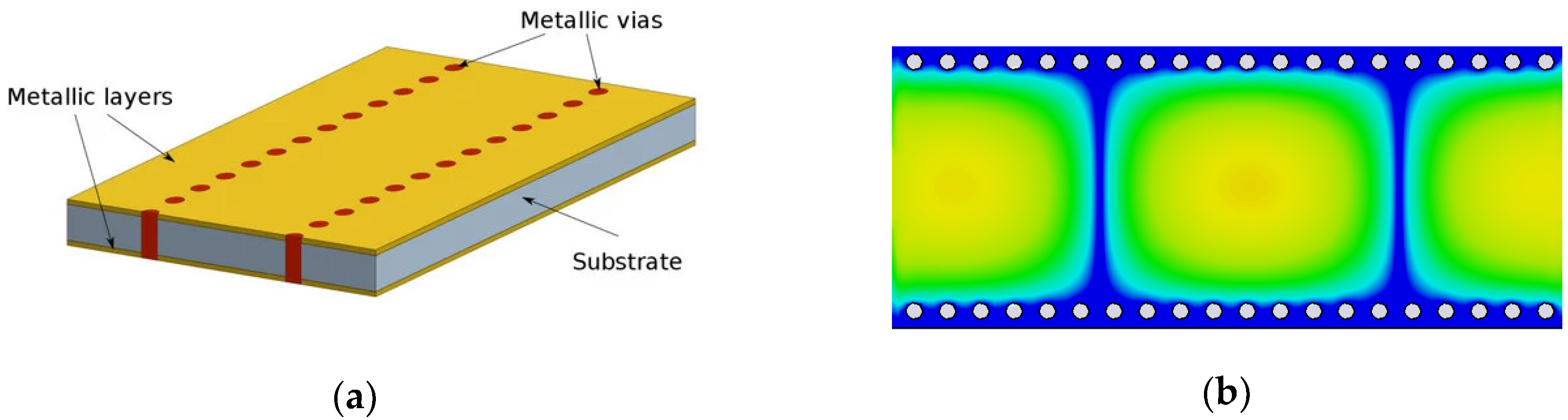
Figure 2.
The fundamental parameters of the SIW Line.
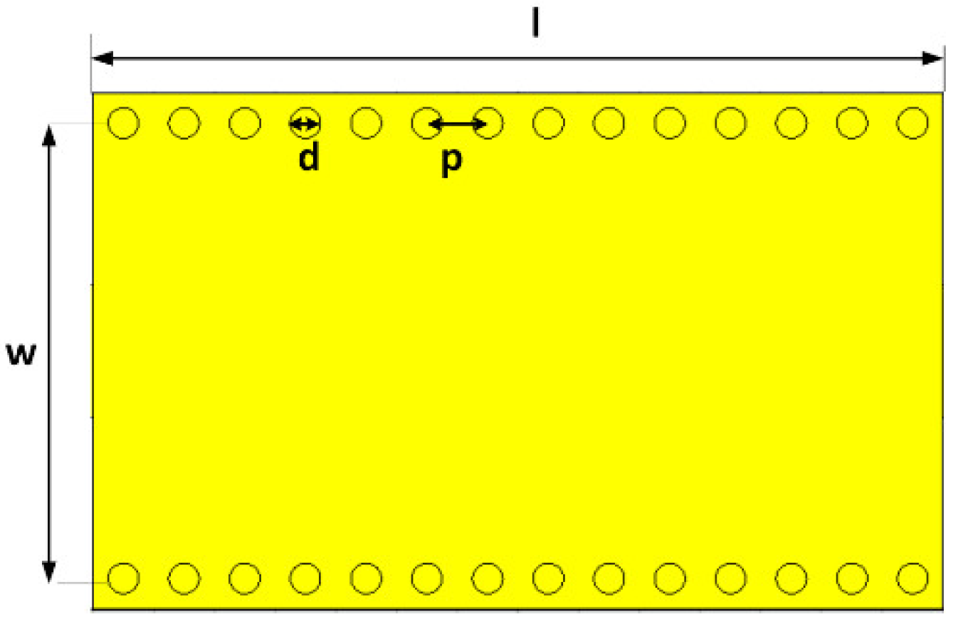
Figure 3.
The Basic Structure of four-port Coupler.
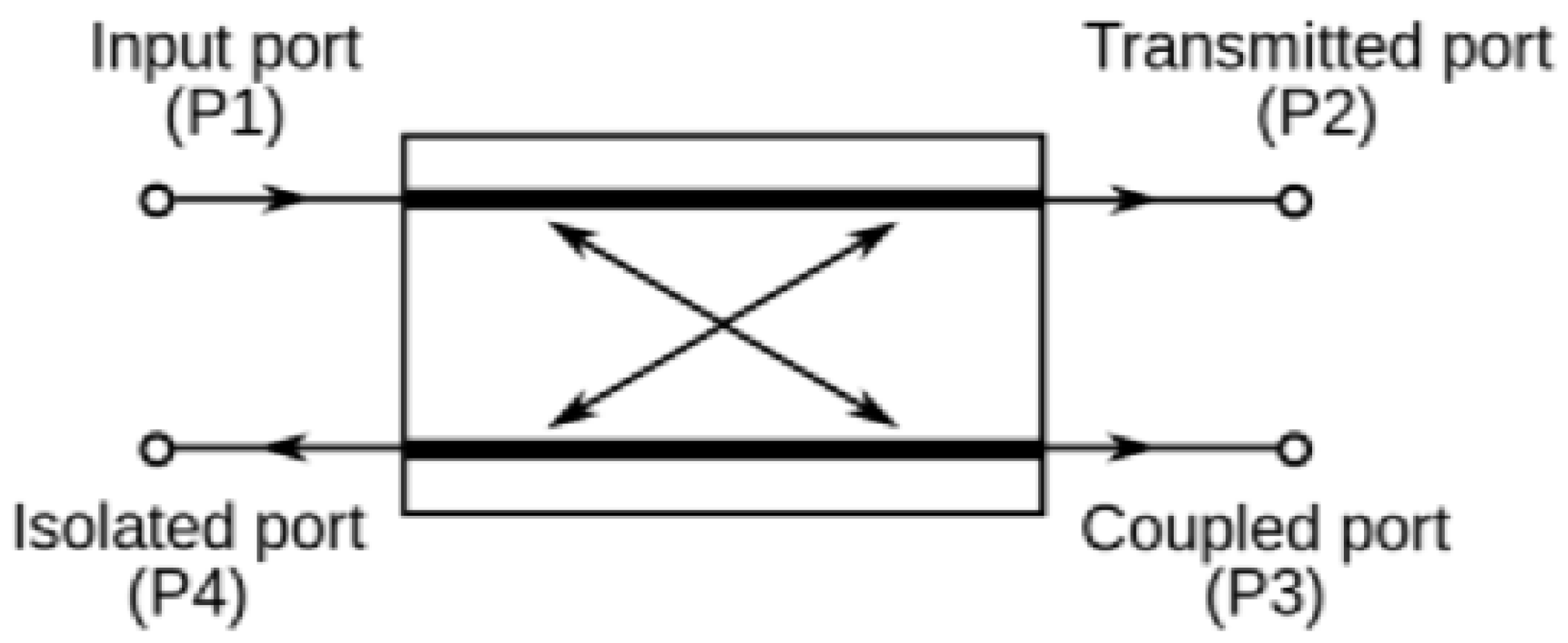
Figure 4.
The Basic Structure of the single-aperture SIW Coupler.
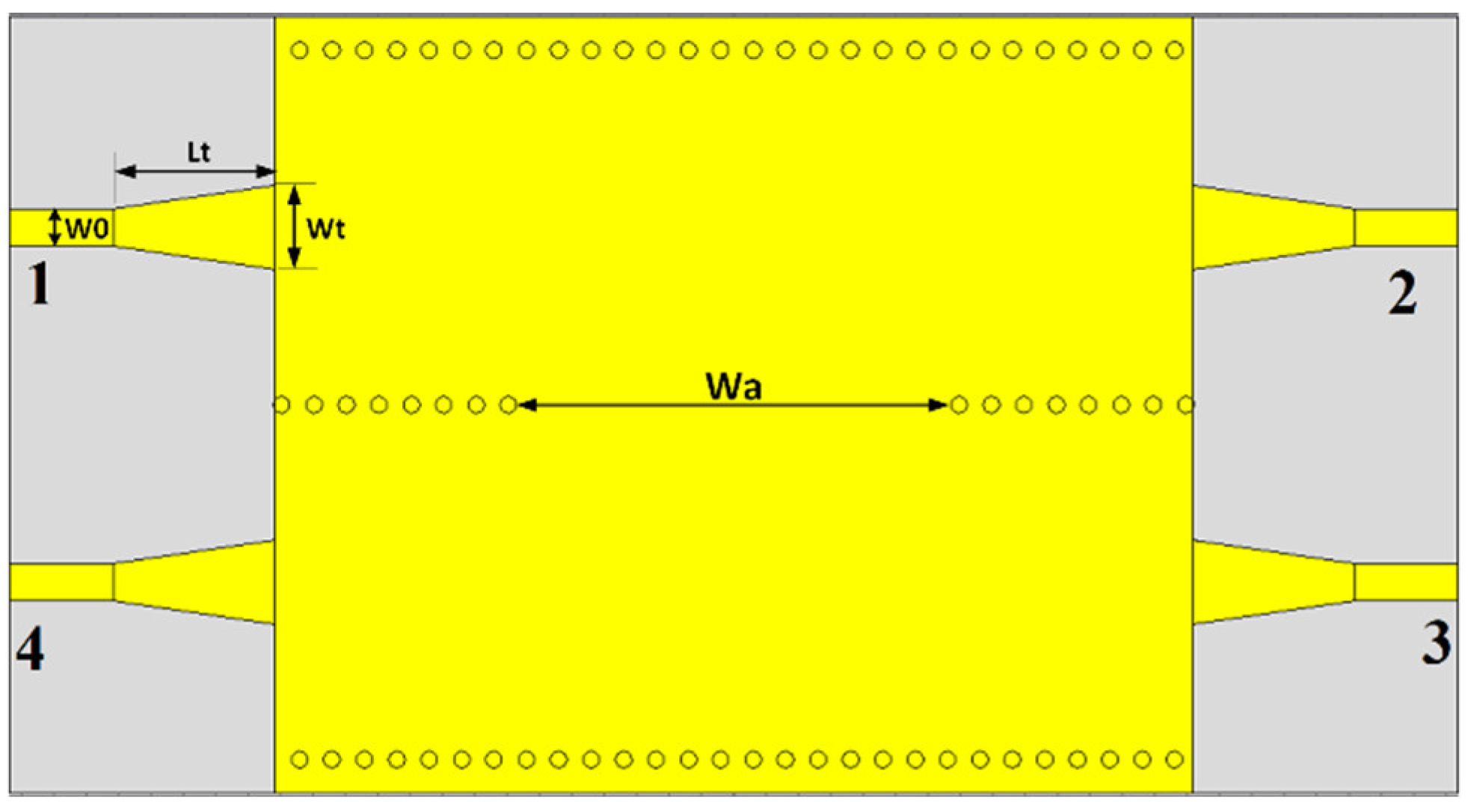
Figure 5.
Simulated S-parameter of the basic X-band Directional Coupler.
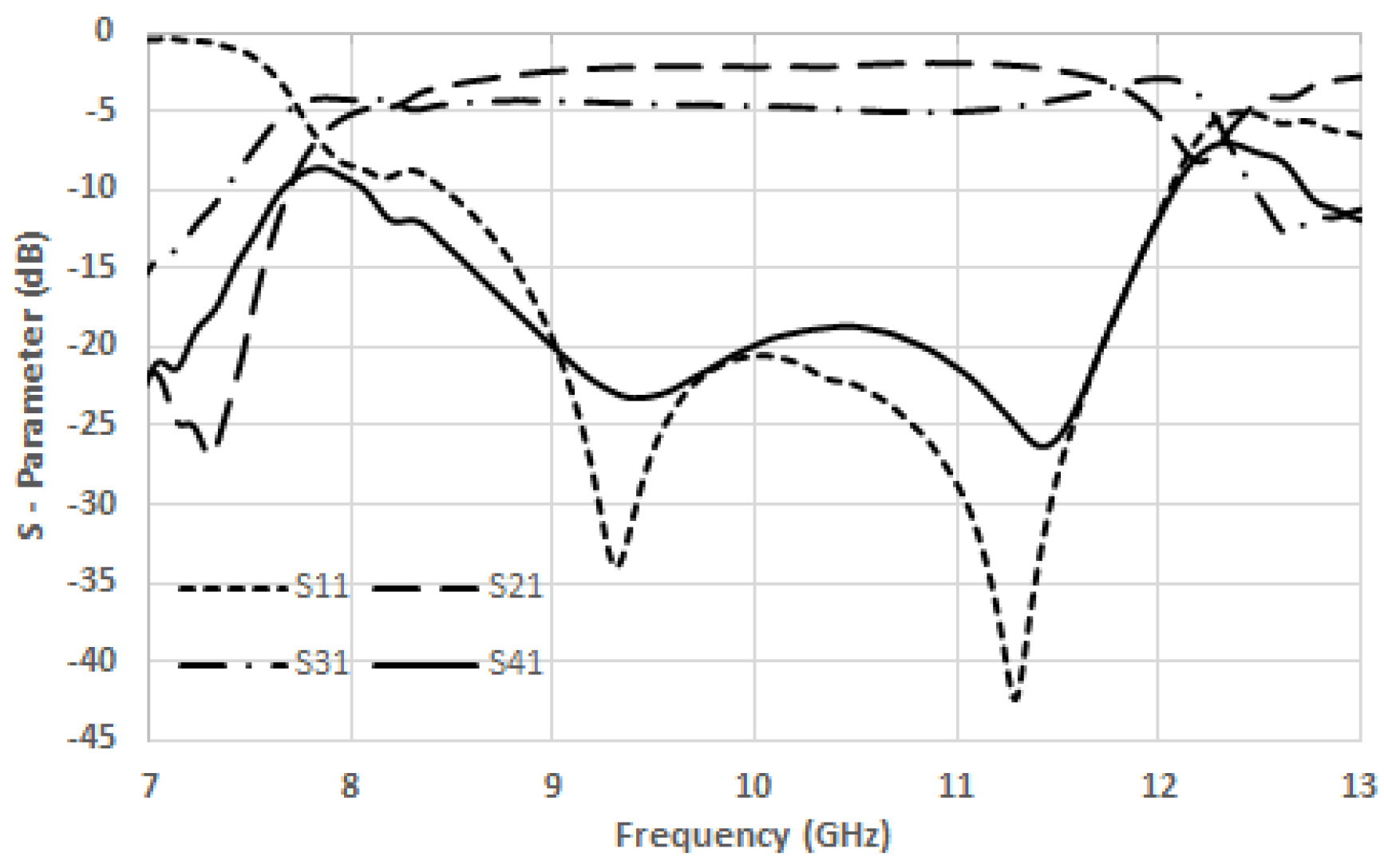
Figure 6.
Simulated electric field distribution of the basic X band coupler at 10 GHz.
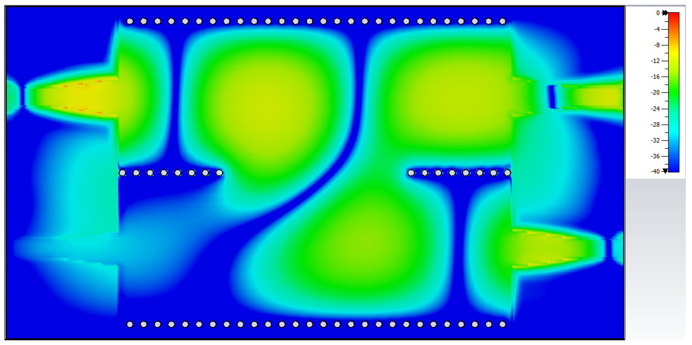
Figure 7.
The structure of proposed SIW coupler.
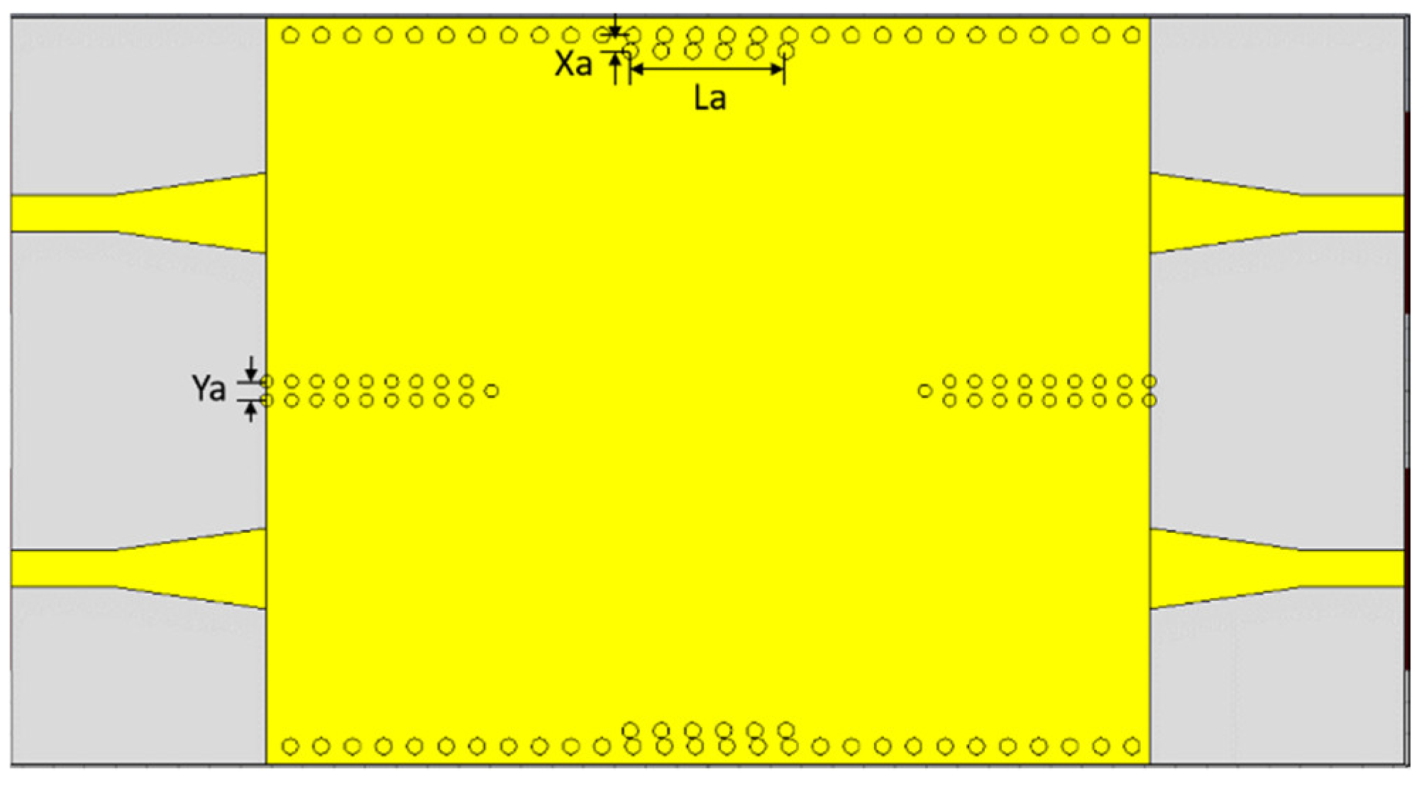
Figure 8.
Effects of Xa of the additional vias on the performance of the coupler: (a) Simulated electric field distribution of the coupler at 9 GHz in the case of Xa = 0.5; (b) Simulated electric field distribution of the coupler at 9 GHz in the case of Xa = 0.8, (c) Simulated electric field distribution of the coupler at 9 GHz in the case of Xa = 1.0; (d) Comparison of S41 simulated results.
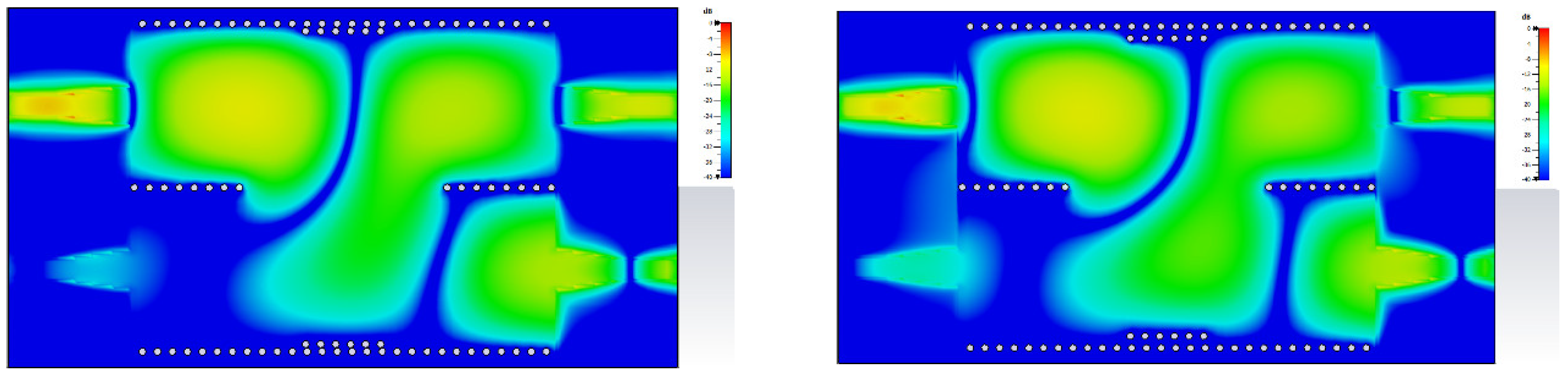
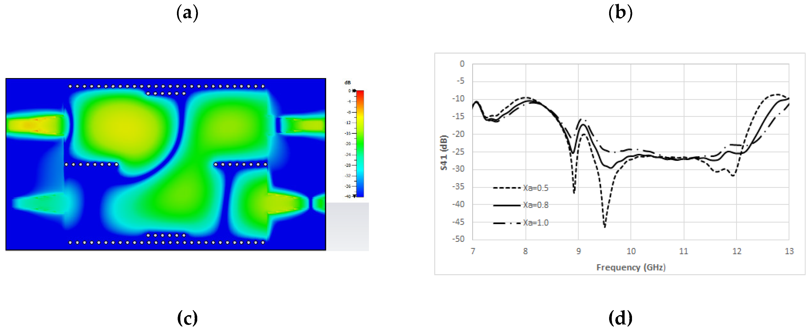
Figure 9.
Simulated S-parameter of the proposed coupler.
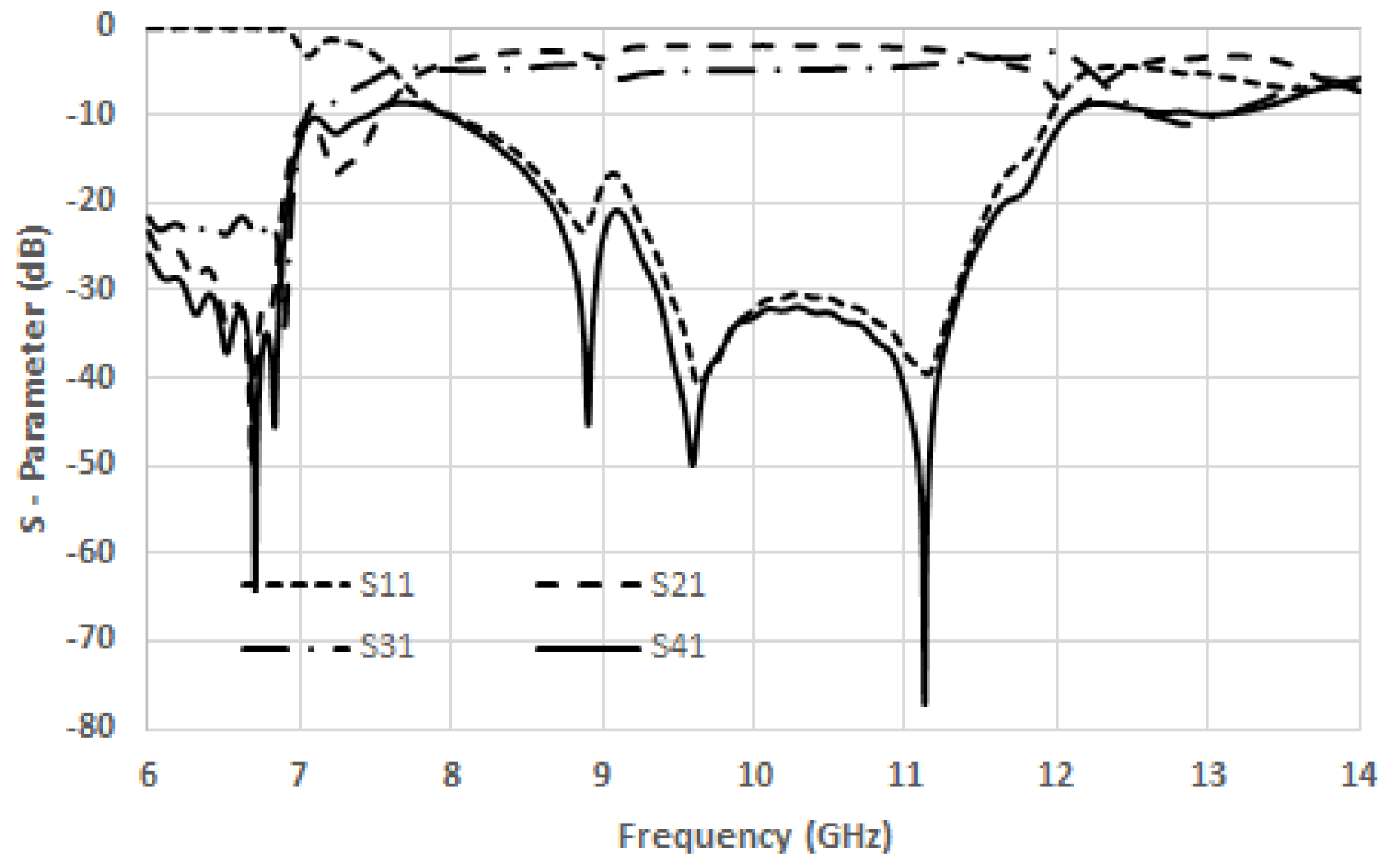
Figure 10.
Simulated electric field distribution of the proposed coupler at 10 GHz.
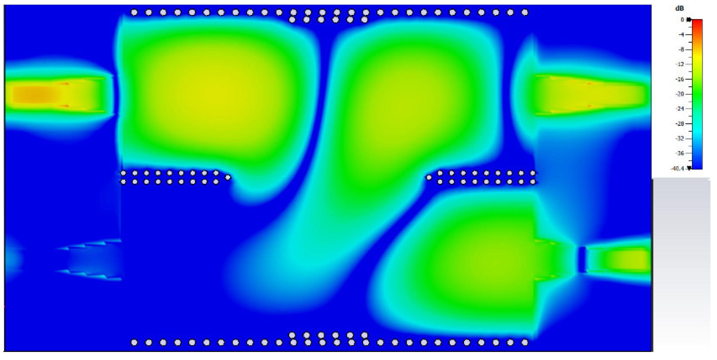
Figure 11.
Simulated S41 of the basic X-band coupler and the proposed coupler.
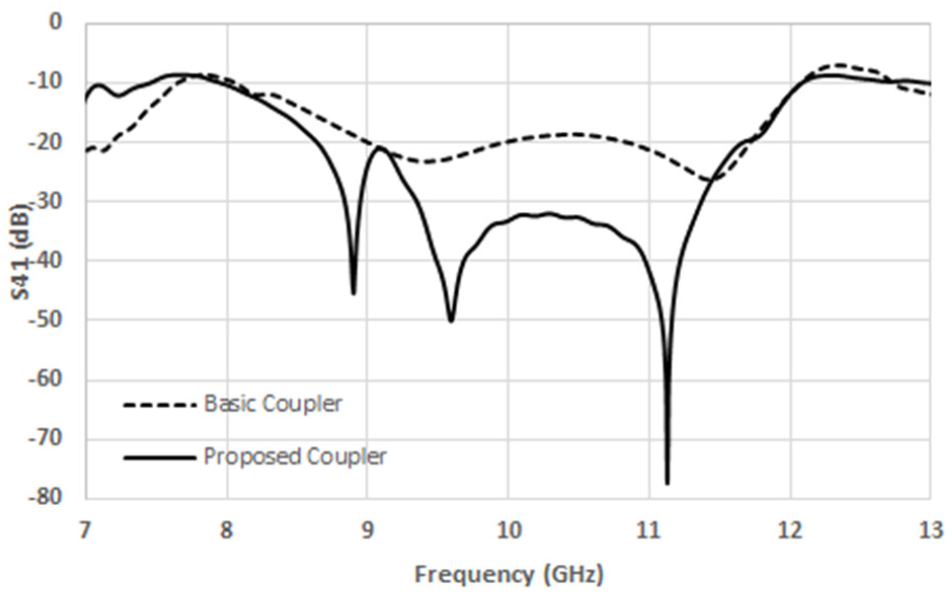
Figure 12.
The photograph of the two fabricated X-band couplers: (a) Basic SIW directional coupler; (b) The high isolation directional coupler.
Figure 12.
The photograph of the two fabricated X-band couplers: (a) Basic SIW directional coupler; (b) The high isolation directional coupler.
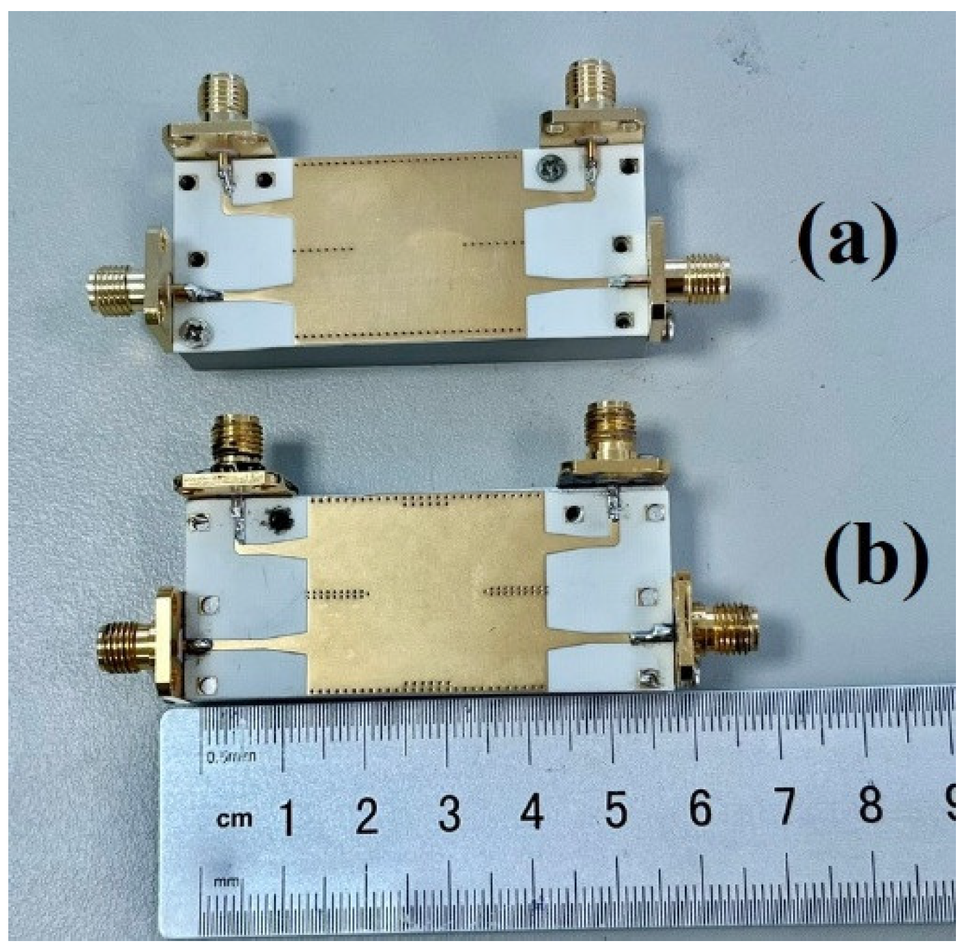
Figure 13.
Measured S-Parameters of the basic X-band coupler.
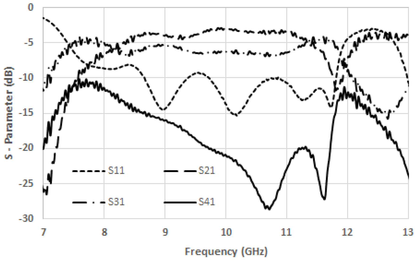
Figure 14.
Measured S-Parameters of the proposed coupler.
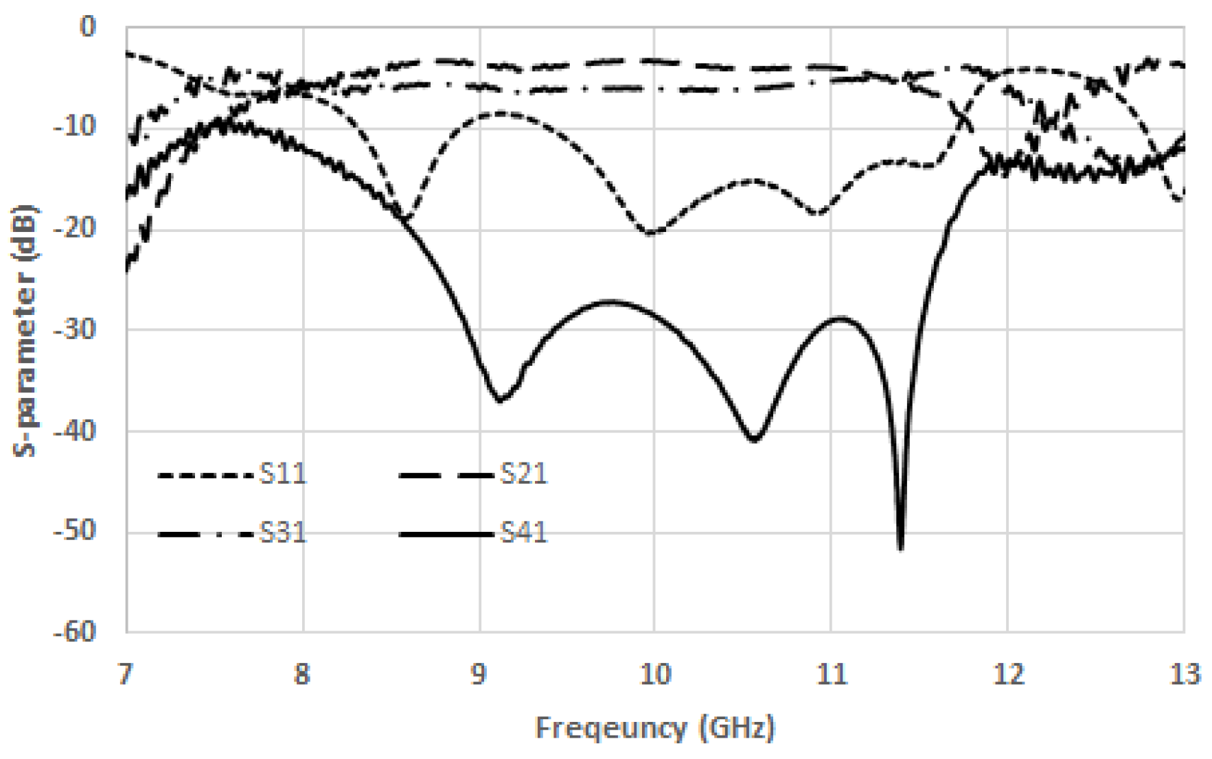
Figure 15.
Measured S41 results of the two couplers.
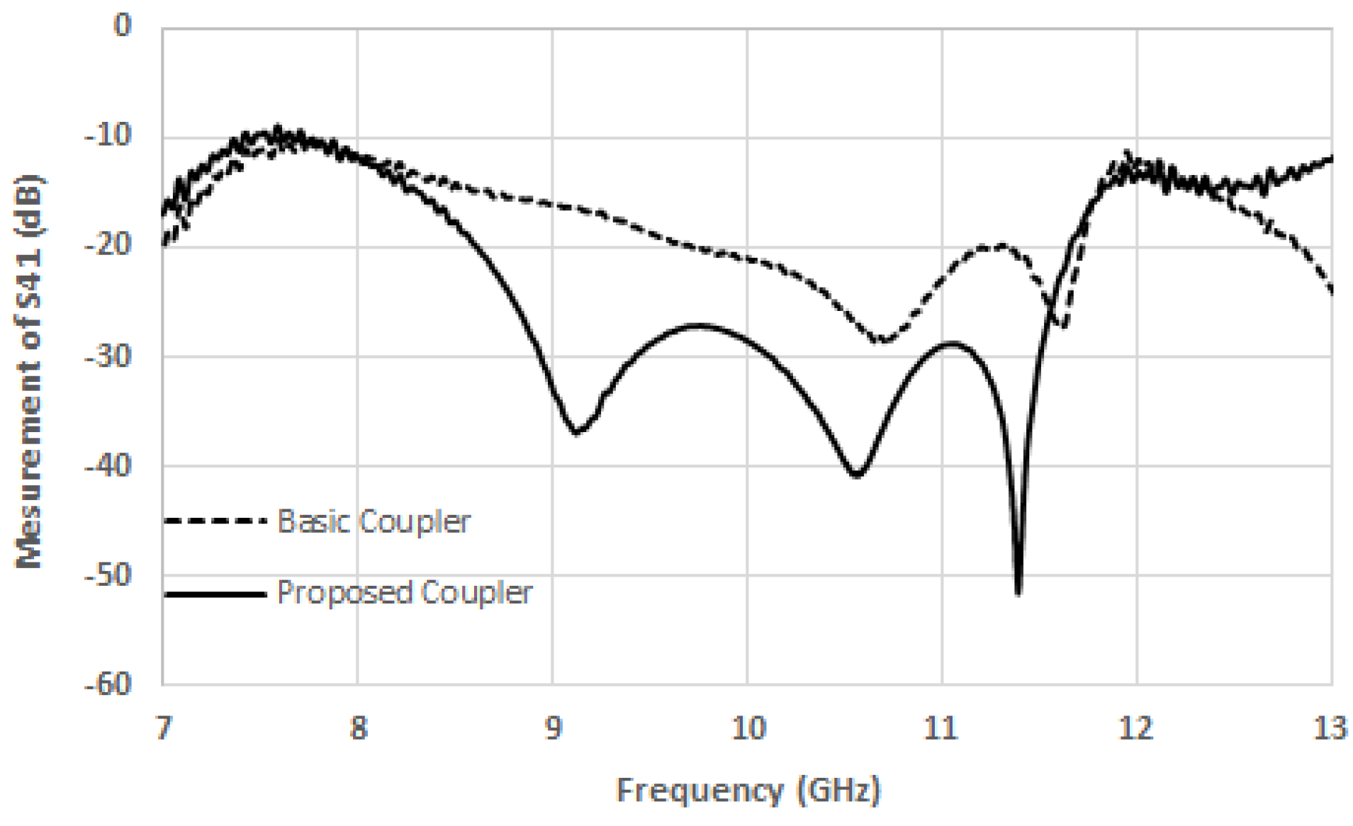

Table 1.
The parameters of single-aperture X-band coupler.
| W | L | d | p | Wa |
|---|---|---|---|---|
| 24 mm | 28.3 mm | 0.5 mm | 1 mm | 13.9 mm |
Table 2.
The parameters of the high isolation X-band coupler.
| 0.6 mm | 5 mm | 0.5 mm |
Table 3.
Comparison table.
| This Work | Ref [9] | Ref [3] | Ref [12] | ||
|---|---|---|---|---|---|
| Simulation results | -32 dB @ 10GHz | -18 dB @ 9GHz | -15 dB | <-15dB @ 35%BW | |
| -2.0 dB @ 10GHz | -3.76 dB @ 9GHz | -3.52 dB | about -4dB | ||
| -4.7 dB @ 10GHz | -3.83 dB @ 9GHz | -6.57 dB | about -4dB | ||
| -33 dB@ 10 GHz | -22 dB @ 9GHz | -26.4 dB | about -20 dB | ||
| Bandwidth | (8.5 - 11.5) GHz | (8.5 - 10.5) GHz | (8.5 - 11) GHz | (7.5-11) GHz | |
| Experimental results | -20.2 dB @ 10GHz | -23 dB @ 8.8GHz | - | <-14dB@32.3%BW | |
| -3.3 dB @ 10GHz | -2.9 dB @ 8.8GHz | - | about -5dB | ||
| -6.0 dB @ 10GHz | -3.2 dB @ 8.8GHz | - | about -5dB | ||
| -28.6 dB @ 10GHz | -27 dB @ 8.8GHz | - | <-14dB@(7.56-10.49)GHz | ||
| Bandwidth | (8.6 - 11.6) GHz | (8.5 - 10.5) GHz | - | (7.5-11) GHz | |
Disclaimer/Publisher’s Note: The statements, opinions and data contained in all publications are solely those of the individual author(s) and contributor(s) and not of MDPI and/or the editor(s). MDPI and/or the editor(s) disclaim responsibility for any injury to people or property resulting from any ideas, methods, instructions or products referred to in the content. |
© 2025 by the authors. Licensee MDPI, Basel, Switzerland. This article is an open access article distributed under the terms and conditions of the Creative Commons Attribution (CC BY) license (http://creativecommons.org/licenses/by/4.0/).
Copyright: This open access article is published under a Creative Commons CC BY 4.0 license, which permit the free download, distribution, and reuse, provided that the author and preprint are cited in any reuse.


