
Submitted:
07 January 2025
Posted:
07 January 2025
You are already at the latest version
Abstract
Energy issues, including energy generation, conversion, transmission and detection, are fundamental factors in all systems. In micro- and nanosystems, dealing with these energy issues requires novel nanostructures and precise technology. However, both concept and setup are not well established yet in the microsystems, especially for those in nanometer scale. Here we demonstrate electromagnetic nanocoils with 100 nanometers in diameter based on uniform and periodic InGaN nanoring arrays grown on patterned GaN surfaces by Nanoscale Selective Area Epitaxy (NSAE). We observed stronger photoluminescence from the periodic InGaN nanoring arrays compared to nonuniform InGaN nanorings, which indicates a good crystal quality of the InGaN nanostructure by the NSAE. Based on this kind of nanostructure, electromagnetic induction from the nanorings is detected from the movement of refractive high-energy electron diffraction patterns in a modulated external magnetic field. Our results clearly show the generation of inductive current and internal magnetic field in the nanorings. We anticipate this kind of nanostructure to be a potential key element for energy conversion, transfer and detection in nanosystems. For example, it could be used to fabricate microtransformers and micro- & nanosensors for electromagnetic signals.
Keywords:
InGaN
; NSAE
; nanoring
; electromagnetic nanocoils
1. Introduction
Low dimensional semiconductor structures such as quantum dots, nanorings and nanowires give rise to new physical phenomena that have been applied in optoelectronic and electronic devices with novel functionalities, such as quantum dot (QD) laser diodes (LDs) [1] and single-electron transistors [2]. In particular, semiconductor nanorings are more complex quantum systems. On the one hand, the inner hole in the semiconductor nanorings provides a capability of trapping a single magnetic flux and offers the exciting opportunity to observe electronic wave-function phases in magneto-optical experiments. Thus, this unique nanostructure has attracted intense interest on quantum interference phenomenon and excitonic Aharonov–Bohm (AB) effect [3,4] in transport and optical properties recently [5,6,7,8,9,10,11,12,13,14,15]. On the other hand, this structure also provides a current path in nanoscale systems, in which a current can be induced, and furthermore, a magnetic field can be generated only in the inner hole. This kind of semiconductor nanocoil is significant for electromagnetic signal generation, detection and energy conversion in integrated nanosystems for optoelectronic and biological applications.
To date, the formation of semiconductor nanorings is often through self-organized processes, mostly controlled by the Stranski-Krastanow (S-K) growth mode [16]. By this method, semiconductor nanorings were fabricated [5,17,18,19,20,21,22]. Some researchers control structure morphology to form nanorings by modulating adatom migration rate, controlling surface free energy balance [23] or using lithographic techniques [7]. However, the random distribution of the ring sizes and locations usually occurred. Besides the S-K mode, some researchers developed a few unique methods to create nanorings. By using polar surface–induced spontaneous self-coiling process, freestanding single-crystal complete nanorings of zinc oxide were formed [24]. Hollow nanocrystals can be synthesized through a mechanism analogous to the Kirkendall Effect, in which pores form because of the difference in diffusion rates between two components in a diffusion couple [25].
In order to achieve uniform and periodic structure arrays, many different surface processing methods were carried out to promote nucleation at expected sites, including surface states control [26,27,28], shallow modulated substrate surfaces [29,30] and nanoscale selective area epitaxy (NSAE) on patterned surfaces [31,32,33,34]. By using the NSAE, we have produced uniform and periodic nanodot/ nanoring/nanowire arrays, which have a mean lateral size less than 100 nm with a standard deviation of only 2.94% for the nanodots/nanorings [35].
Here, we present the work on electromagnetic induction from the long-range ordered InGaN nanoring arrays on the patterned GaN surface. The nanopatterns were defined by electron-beam lithography (EBL). The InGaN nanoring arrays were grown by the NSAE in metalorganic chemical vapour deposition (MOCVD). The electromagnetic induction from the nanorings was detected by the movement of refractive high-energy electron diffraction (RHEED) in a modulated external magnetic field.
2. Materials and Methods
To fabricate the nanostructures, first a semi-insulating GaN film was grown on a c-plane sapphire up to a thickness of 2 μm. Next 80 nm SiO2 was deposited onto the GaN film, and then processed by EBL to create nanopatterns in the SiO2. The fabrication details have been described elsewhere [34,35], Supporting Online Material: Figure S1. InGaN was then grown on the patterned SiO2/GaN in the MOCVD reactor at 750 ℃, resulting in the formation of nanodots or nanorings, depending on the pattern sizes and growth durations. The nominal thickness of the InGaN is about 10 nm. On top of the InGaN, another 10 nm GaN cap layer was grown. Finally, the samples were dipped in diluted hydrofluoric acid to remove all SiO2 to assess the sample morphology. The samples were investigated by means of scanning electron microscopy (SEM), continues wave (CW) photoluminescence (PL) at low temperature and RHEED at 200 ℃.
A typical SEM image of the InGaN nanoring arrays grown on the patterned GaN surface is shown (Figure 1). The nanorings are about 100 nm in diameter and spaced by 200 nm. The inset is a three-dimensional view of a few nanorings. In this sample, the InGaN nanorings are well developed. The InGaN nanorings have very uniform size and regular symmetry. The standard deviation of the nanorings in diameter is around 3%.
3. Results
PL spectra from the 100 nm InGaN nanoring arrays were obtained (Figure 2) under different excitation levels of 0.1I0, 0.8I0 and I0, where I0 is the highest excitation power. The excitation source is a 325 nm He-Cd CW laser. It is seen that the emission from the nanorings is broad. The fringes in the spectra are caused by light interference in the epilayer. Clearly, the broadening is not due to the size non-uniformity, but due to the nonuniform indium composition across the ring. The ring-shape profile indicates the different growth rates between the edge area and centre area in those patterned holes. Furthermore, the indium composition is influenced by the growth rate. A higher growth rate induced higher indium incorporation efficiency in this experiment. As shown in Figure 2, by increasing the excitation power, the emission at the shorter wavelength part (around 460 nm) was enhanced more than the part in longer wavelength range (around 500 nm), which indicates more excitons recombining at higher energy levels under higher excitation power. Due to the large photo-energy difference between 460 nm (2.70 eV) and 500 nm (2.48 eV), this photo energy increment cannot be fully explained by band filling effect. So, it means that the indium composition is not uniform in a nanoring. According to the growth rate difference in a nanohole, it is deemed that a higher growth rate at the edge area results in a higher indium composition. The indium accumulation effect at the edge area can be directly observed in the growth with a larger selective area (Supporting Online Material: Figure S2). Thus, these InGaN structures not only have ring-shape profile in geometry image, but also a ring-shape potential in energy picture. From the PL results, the largest potential is about 820 meV deep with reference to the semi-insulating GaN layer.
It is well known that normal InGaN by epitaxy is unintentionally n-type semiconductor. The InGaN nanorings also are not exceptional and have free electrons with a concentration of 1018 ~ 1019/cm3 estimated from InGaN epilayers at room temperature. Namely, there should be a few hundred free electrons in a single InGaN nanoring. Once these electrons flow along the ring, there will be an additional magnetic field generated by the ring current. To observe electromagnetic induction from the nanorings, we plan to create the ring current by modulating the external magnetic field.
The electromagnetic induction from the InGaN nanorings is measured by RHEED in a high vacuum chamber (~ 10-9 Torr). The movement of the RHEED patterns is recorded by RHEED monitoring software. The sample is mounted on a Molybdenum holder equipped with a heater at the backside. Because the heater is a wreathed filament, it can provide a modulated external magnetic field by flowing a DC current. To confirm the environment is clean for the RHEED measurement, i.e. without any other source to generate a magnetic field, a bare GaN/sapphire sample is used for reference.
After desorption of all impurities by keeping the sample in the high vacuum chamber for 24 hours, the samples were heated to 200 ℃ for RHEED. The RHEED patterns from the InGaN nanoring surface and the bare GaN surface were obtained respectively (Figure 3, a and b) without external magnetic field. As expected, spotty patterns were observed on the InGaN nanoring surface (Figure 3a), while streaky patterns were observed on the bare GaN surface (Figure 3b). When an external magnetic field is exerted, these patterns will shift in the direction as indicated by the white arrows in Figure 3. Obviously, the shifting of the patterns is decided by how the external magnetic field alters. In order to record how the patterns shift, we choose to record the time-dependent light intensity of a pattern in the selected area, as indicated by the white box in Figure 3. When the pattern moves away, the light intensity drops. However, if there is any undulation during the movement of the pattern, so is the intensity recorded. In this experiment, the external magnetic field is modulated by the heater current switched between 0 A and 17 A.
The intensity change in the presence of the external magnetic field has been recorded (Figure 4). For the bare GaN reference sample, the intensity dropped monotonously till to the background value, which indicates that the bare GaN does not generate any induced magnetic field. This can be easily understood, since the GaN is semi-insulating and does not have any ring-shape potential to confine the movement of electrons. However, the intensity evolvement is different for the InGaN nanoring surface - there are several rebounds during the intensity drop, as marked by the stars in Figure 4. These rebounds indicate that the patterns were not monotonously shifting in direction; instead, the patterns have been pulled back a little during the shift. This indicates the existence of an additional magnetic field generated during the process. The only source for the new magnetic field is the InGaN nanoring arrays. A ring current is first induced in the InGaN nanorings during the increase/decrease of the external magnetic field. In turn, the ring current produces the new magnetic field. Because the increase/decrease of the external magnetic field is not linear, the ring current density and the induced magnetic field intensity were varying during the process. The direction of the induced magnetic field can be the same or opposite to the external magnetic field. Indeed, we observed several rebounds during one shift, which indicates the variation of the induced magnetic field. For whole process of the shift, please refer to the video clips attached in the Supporting Online Material. This phenomenon proves the electromagnetic induction from the InGaN nanorings, acting as electromagnetic nanocoils.
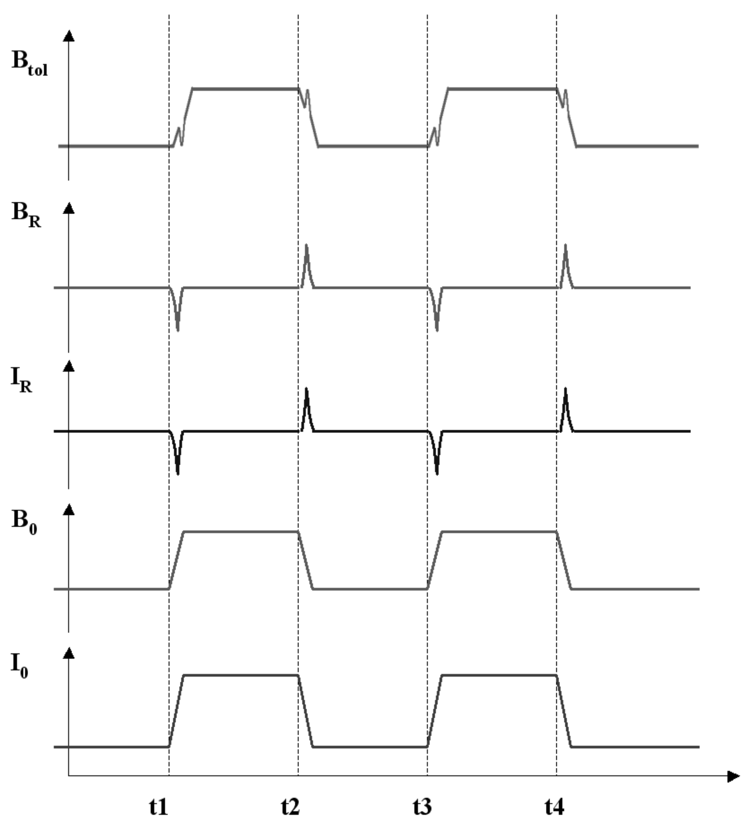
The detailed process is schematically described (Figure 5). The external magnetic field (B0) is modulated by turning on and off the DC current (I0) of 17 A through the heater. A linear variation of B0 is assumed. Due to the ring-shape InGaN nanostructure existing in the magnetic field, an inductive ring current (IR) will be induced in the nanorings during the appearance and disappearance of B0. Furthermore, the inductive ring current, IR, generates an additional magnetic field (BR) that can be the same or opposite to B0. Thus, in this system, the total magnetic field (Btol) is the vector sum of B0 and BR (Figure 5). The movement of the RHEED patterns embodies the behaviour of the total magnetic field in this system. Appearing and disappearing of the B0 cause the major shift of the RHEED patterns. When there is no other magnetic field source, B0 is the only factor to cause the shift of RHEED patterns, as in the case of the bare GaN sample. However, IR and BR will be induced on the InGaN nanoring surface, and BR will also contribute to Btol. Thus, in this case, the movement of the RHEED patterns also presents the influence from BR.
4. Conclusions
In this study, the InGaN nanorings show the capability of generating ring current and magnetic field in the nanoscale. Based on this nanostructure and phenomenon, a variety of nanodevices and nanosystems can be built, which can work under either active or passive mode serving various functionalities. In the active mode, i. e. when the ring current is artificially injected, the nanorings can produce magnetic field that is concentrated in the ring. In this case, the nanorings could work as a nanotransmitter, which can transfer energy over a space to a receiver through its magnetic field. If the receiver consists of multiple-ring structures, then the whole nanosystem can work as a nanotransformer. In the passive mode, i.e. when the ring current is induced by an external magnetic field, the nanoring arrays could be used as nanoscale sensors, transducers and resonators.6. Patents
The demonstration of uniform and periodic InGaN nanoring arrays by NSAE presented here should be universal and transferable to other materials and structures [35]. The successful demonstration of electromagnetic induction based on the nanorings may not only benefit fundamental study on quantum effects, but also open a way for energy conversion, transfer and detection in nanosystems.
Supplementary Materials
The following supporting information can be downloaded at the website of this paper posted on Preprints.org, Figure S1: Formation of InGaN nanorings; Figure S2: The sample structure, cathode luminescence (CL) experiment and CL results for the investigation of indium accumulation effect; Video S1: The RHEED pattern movements on the bare GaN surface when the external magnetic field is applied. The patterns monotonously move to another position; Video S2: The RHEED pattern movements on the InGaN nanoring surface when the external magnetic field IS APPLIED. There are several rebounds during the patterns shift; Video S3: The RHEED pattern movements on the InGaN nanoring surface when the external magnetic field IS REMOVED. There also are several rebounds during the patterns shift.
Author Contributions
Conceptualization, P.C.; formal analysis, Z.Y.; methodology, Z.Y., X.Z, Z.X., D.C.,X.X and H.Z ; software, Z.Y., and; investigation, P.C.; resources, P.C.; data curation, P.C.; writing—original draft preparation, P.C.; writing—review and editing, P.C.; supervision, Y.S.,R.Z. and Y.Z; project administration, P.C.; funding acquisition, P.C. All authors have read and agreed to the published version of the manuscript.
Funding
This work is supported by National Nature Science Foundation of China, grant number 12074182, Collaborative Innovation Center of Solid-State Lighting and Energy-saving Electronics and Open Fund of the State Key Laboratory on Integrated Optoelectronics, grant number IOSKL2017KF03.
Data Availability Statement
All data, theory detail, simulation detail that support the findings of this study are available from the corresponding authors upon reasonable request.
Acknowledgments
The authors acknowledge Nanjing University and Jiangsu Provincial Key Laboratory of Advanced Photonic and Electronic Materials for their support in advanced micro technology and clean room facilities.
Conflicts of Interest
The authors declare no conflict of interest.
References
- Fafard, S.; Hinzer, K.; Raymond, S.; Dion, M.; McCaffrey, J.; Feng, Y.; Charbonneau, S. Red-Emitting Semiconductor Quantum Dot Lasers. Science 1996, 274, 1350–1353. [Google Scholar] [CrossRef]
- Devoret, M.H.; Schoelkopf, R.J. Amplifying quantum signals with the single-electron transistor. Nature 2000, 406, 1039–1046. [Google Scholar] [CrossRef]
- Chaplik, A.V. Magnetoexcitons in quantum rings and in antidots. 1995, 62, 900.
- Aharonov, Y.; Bohm, D. Significance of Electromagnetic Potentials in the Quantum Theory. Physical Review 1959, 115, 485–491. [Google Scholar] [CrossRef]
- Lorke, A.; Luyken, R.J.; Govorov, A.O.; Kotthaus, J.P.; Garcia, J.M.; Petroff, P.M. Spectroscopy of Nanoscopic Semiconductor Rings. Physical Review Letters 2000, 84, 2223–2226. [Google Scholar] [CrossRef]
- Warburton, R.J.; Schaflein, C.; Haft, D.; Bickel, F.; Lorke, A.; Karrai, K.; Garcia, J.M.; Schoenfeld, W.; Petroff, P.M. Optical emission from a charge-tunable quantum ring. Nature 2000, 405, 926–929. [Google Scholar] [CrossRef]
- Bayer, M.; Korkusinski, M.; Hawrylak, P.; Gutbrod, T.; Michel, M.; Forchel, A. Optical Detection of the Aharonov-Bohm Effect on a Charged Particle in a Nanoscale Quantum Ring. Physical Review Letters 2003, 90, 186801. [Google Scholar] [CrossRef]
- Römer, R.A.; Raikh, M.E. Aharonov-Bohm effect for an exciton. Physical Review B 2000, 62, 7045–7049. [Google Scholar] [CrossRef]
- Moulopoulos, K.; Constantinou, M.J.P.R.B. Two interacting charged particles in an Aharonov-Bohm ring : Bound state transitions, symmetry breaking, persistent currents, and Berry's phase. 2004, 70.
- Song, J.; Ulloa, S.E. Magnetic field effects on quantum ring excitons. Physical Review B 2001, 63, 125302. [Google Scholar] [CrossRef]
- Maslov, A.V.; Citrin, D.S. Enhancement of the Aharonov-Bohm effect of neutral excitons in semiconductor nanorings with an electric field. Physical Review B 2003, 67, 121304. [Google Scholar] [CrossRef]
- Hu, H.; Zhu, J.-L.; Li, D.-J.; Xiong, J.-J. Aharonov-Bohm effect of excitons in nanorings. Physical Review B 2001, 63, 195307. [Google Scholar] [CrossRef]
- Govorov, A.O.; Ulloa, S.E.; Karrai, K.; Warburton, R.J. Polarized excitons in nanorings and the optical Aharonov-Bohm effect. Physical Review B 2002, 66, 081309. [Google Scholar] [CrossRef]
- Barticevic, Z.; Fuster, G.; Pacheco, M. Effect of an electric field on the Bohm-Aharonov oscillations in the electronic spectrum of a quantum ring. Physical Review B 2002, 65, 193307. [Google Scholar] [CrossRef]
- da Silva, L.G.G.V.D.; Ulloa, S.E.; Govorov, A.O. Impurity effects on the Aharonov-Bohm optical signatures of neutral quantum-ring magnetoexcitons. Physical Review B 2004, 70, 155318. [Google Scholar] [CrossRef]
- Eaglesham, D.J.; Cerullo, M. Dislocation-free Stranski-Krastanow growth of Ge on Si(100). Physical Review Letters 1990, 64, 1943–1946. [Google Scholar] [CrossRef] [PubMed]
- Garcı, J.M.; Medeiros-Ribeiro, G.; Schmidt, K.; Ngo, T.; Feng, J.L.; Lorke, A.; Kotthaus, J.; Petroff, P.M. Intermixing and shape changes during the formation of InAs self-assembled quantum dots. Applied Physics Letters 1997, 71, 2014–2016. [Google Scholar] [CrossRef]
- Garcı, J.M.; Silveira, J.P.; Briones, F. Strain relaxation and segregation effects during self-assembled InAs quantum dots formation on GaAs(001). Applied Physics Letters 2000, 77, 409–411. [Google Scholar] [CrossRef]
- Warburton, R.J.; Schäflein, C.; Haft, D.; Bickel, F.; Lorke, A.; Karrai, K.; Garcia, J.M.; Schoenfeld, W.; Petroff, P.M. Optical emission from single, charge-tunable quantum rings. Physica E: Low-dimensional Systems and Nanostructures, 2001; 9, 124–130. [Google Scholar]
- Luyken, A.L.J.; Garcia, J.M.; Petroff, P.M. Growth and Electronic Properties of Self-Organized Quantum Rings. Japanese Journal of Applied Physics 2001, 40, 1857. [Google Scholar] [CrossRef]
- Blossey, R.; Lorke, A. Wetting droplet instability and quantum ring formation. Physical Review E 2002, 65, 021603. [Google Scholar] [CrossRef] [PubMed]
- Granados, D.; Garcı, J.M. In(Ga)As self-assembled quantum ring formation by molecular beam epitaxy. Applied Physics Letters 2003, 82, 2401–2403. [Google Scholar] [CrossRef]
- Raz, T.; Ritter, D.; Bahir, G. Formation of InAs self-assembled quantum rings on InP. Applied Physics Letters 2003, 82, 1706–1708. [Google Scholar] [CrossRef]
- Kong, X.Y.; Ding, Y.; Yang, R.; Wang, Z.L. Single-Crystal Nanorings Formed by Epitaxial Self-Coiling of Polar Nanobelts. Science 2004, 303, 1348–1351. [Google Scholar] [CrossRef] [PubMed]
- Yin, Y.; Rioux, R.M.; Erdonmez, C.K.; Hughes, S.; Somorjai, G.A.; Alivisatos, A.P. Formation of Hollow Nanocrystals Through the Nanoscale Kirkendall Effect. Science 2004, 304, 711–714. [Google Scholar] [CrossRef]
- Mano, T.; Nötzel, R.; Hamhuis, G.J.; Eijkemans, T.J.; Wolter, J.H. Formation of InAs quantum dot arrays on GaAs (100) by self-organized anisotropic strain engineering of a (In,Ga)As superlattice template. Applied Physics Letters 2002, 81, 1705–1707. [Google Scholar] [CrossRef]
- Brune, H.; Giovannini, M.; Bromann, K.; Kern, K. Self-organized growth of nanostructure arrays on strain-relief patterns. Nature 1998, 394, 451–453. [Google Scholar] [CrossRef]
- Facsko, S.; Dekorsy, T.; Koerdt, C.; Trappe, C.; Kurz, H.; Vogt, A.; Hartnagel, H.L. Formation of Ordered Nanoscale Semiconductor Dots by Ion Sputtering. Science 1999, 285, 1551–1553. [Google Scholar] [CrossRef]
- Schmidt, O.G.; Jin-Phillipp, N.Y.; Lange, C.; Denker, U.; Eberl, K.; Schreiner, R.; Gräbeldinger, H.; Schweizer, H. Long-range ordered lines of self-assembled Ge islands on a flat Si (001) surface. Applied Physics Letters 2000, 77, 4139–4141. [Google Scholar] [CrossRef]
- Kiravittaya, S.; Heidemeyer, H.; Schmidt, O.G. Growth of three-dimensional quantum dot crystals on patterned GaAs (001) substrates. Physica E: Low-dimensional Systems and Nanostructures, 2004; 23, 253–259. [Google Scholar]
- Kiravittaya, S.; Schmidt, O.G. ; Comment on “A growth pathway for highly ordered quantum dot arrays” [Appl. Phys. Lett. 85, 5974 (2004)]. Applied Physics Letters, 2005; 86, 206101. [Google Scholar]
- Kim, S.-W.; Ueda, M.; Funato, M.; Fujita, S.; Fujita, S. Artificial control of ZnO nanodots by ion-beam nanopatterning. Journal of Applied Physics 2005, 97, 104316. [Google Scholar] [CrossRef]
- Ishikawa, T.; Kohmoto, S.; Nishimura, T.; Asakawa, K. In situ electron-beam processing for III–V semiconductor nanostructure fabrication. Thin Solid Films 2000, 373, 170–175. [Google Scholar] [CrossRef]
- Chen, P.; Chua, S.J.; Wang, Y.D.; Sander, M.D.; Fonstad, C.G. InGaN nanorings and nanodots by selective area epitaxy. Applied Physics Letters 2005, 87, 143111. [Google Scholar] [CrossRef]
- Chen, A.; Chua, S.J.; Chen, P.; Chen, X.Y.; Jian, L.K. Fabrication of sub-100 nm patterns in SiO2 templates by electron-beam lithography for the growth of periodic III–V semiconductor nanostructures. Nanotechnology 2006, 17, 3903. [Google Scholar] [CrossRef]
Figure 1.
SEM image of the InGaN nanoring arrays grown on the patterned GaN surface. The nanorings are around 100 nm in diameter and spaced by 200 nm. The inset is a three-dimensional view of a few nanorings.
Figure 1.
SEM image of the InGaN nanoring arrays grown on the patterned GaN surface. The nanorings are around 100 nm in diameter and spaced by 200 nm. The inset is a three-dimensional view of a few nanorings.
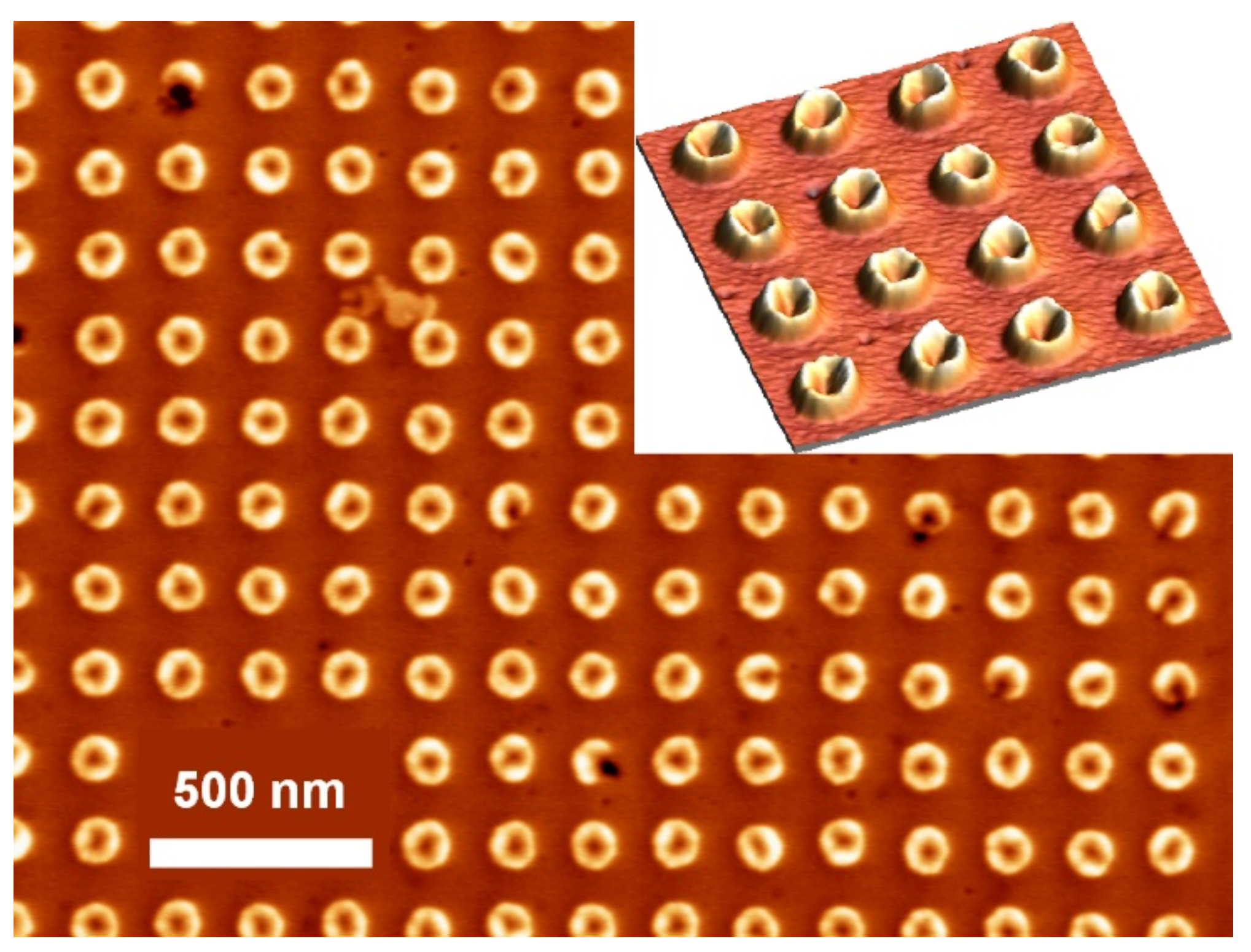
Figure 2.
Low-temperature (77 K) PL spectra from the InGaN nanoring arrays with 100 nm diameter under different excitation levels of 0.1I0, 0.8I0 and I0, where I0 is the highest excitation power.
Figure 2.
Low-temperature (77 K) PL spectra from the InGaN nanoring arrays with 100 nm diameter under different excitation levels of 0.1I0, 0.8I0 and I0, where I0 is the highest excitation power.
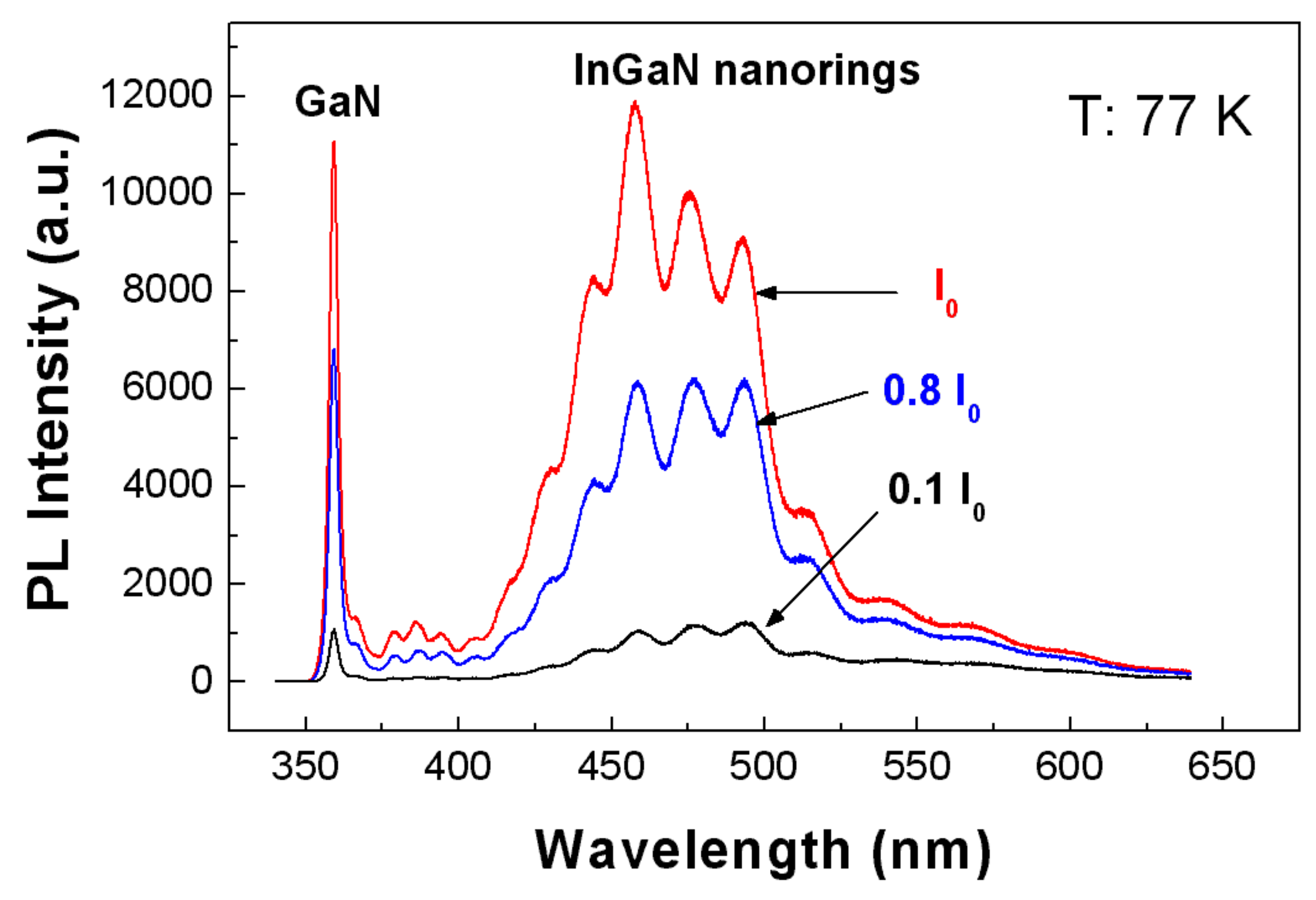
Figure 3.
RHEED patterns from (a) InGaN nanoring surface and (b) bare GaN surface without external magnetic field. Spotty patterns were observed on the InGaN nanoring surface and streaky patterns were observed on the bare GaN surface. The white arrows indicate the movement of these patterns under a magnetic field. The white boxes indicate the areas in which the time-dependent intensity is recorded when the magnetic field is applied. .
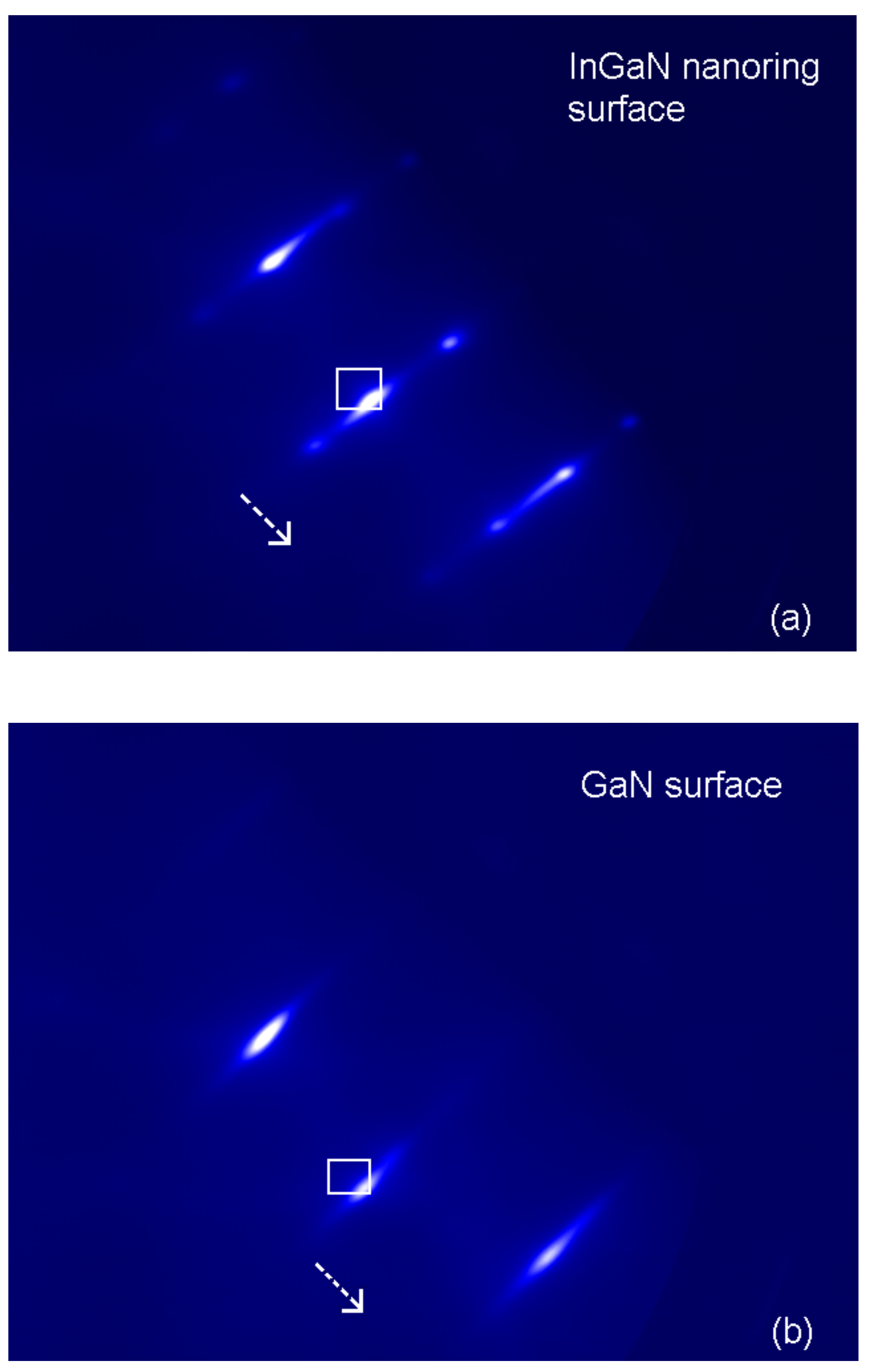
Figure 4.
Intensity change of the monitored areas shown in Figure 3. when the external magnetic field is applied. On the bare GaN surface, the intensity drops monotonously to the background value, which indicates a straightforward shift of the pattern. On the nanoring surface, the intensity shows small rebounds during its decrease process, which indicates the return movement of the pattern.
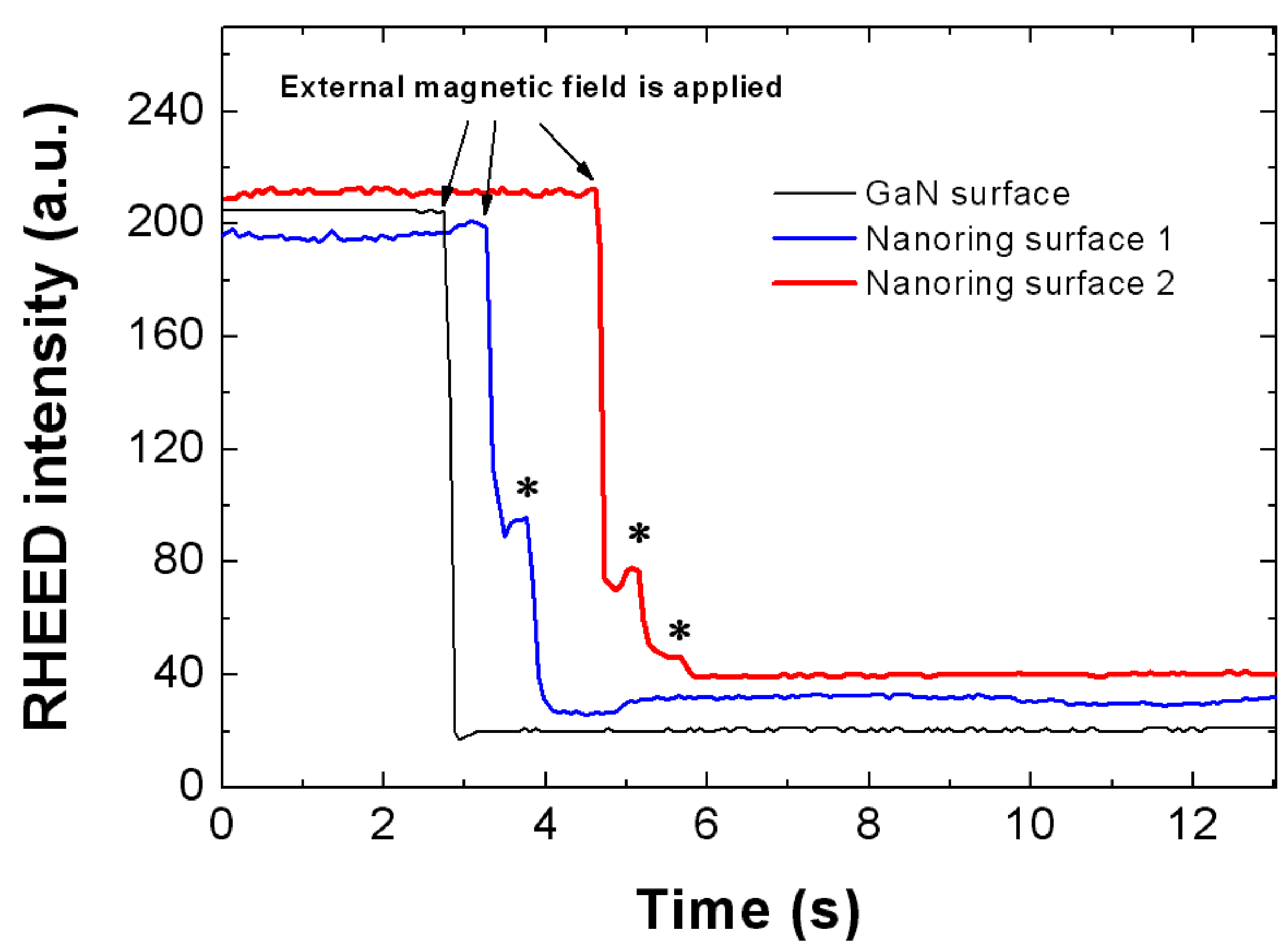
Figure 5.
Schematic description of the electromagnetic induction process. I0 is the DC current through the heater. B0 is the external magnetic field, which is modulated by “on” and “off” the I0. IR is the inductive ring current in the InGaN nanorings during the B0 changing. BR is the inductive magnetic field generated by the IR. Btol is the total magnetic field, which is the vector sum of B0 and BR.
Disclaimer/Publisher’s Note: The statements, opinions and data contained in all publications are solely those of the individual author(s) and contributor(s) and not of MDPI and/or the editor(s). MDPI and/or the editor(s) disclaim responsibility for any injury to people or property resulting from any ideas, methods, instructions or products referred to in the content. |
© 2025 by the authors. Licensee MDPI, Basel, Switzerland. This article is an open access article distributed under the terms and conditions of the Creative Commons Attribution (CC BY) license (http://creativecommons.org/licenses/by/4.0/).
Copyright: This open access article is published under a Creative Commons CC BY 4.0 license, which permit the free download, distribution, and reuse, provided that the author and preprint are cited in any reuse.


