Submitted:
16 December 2024
Posted:
18 December 2024
You are already at the latest version
Abstract
The current mirror (CM) is a fundamental building block in analog circuit design, primarily used to replicate a reference current at the output terminal, ensuring that the output current closely matches the input current. CMs are crucial in integrated circuits, performing tasks such as current steering, biasing, and active load implementation. In an ideal scenario, the output current should precisely mirror the input current, while the output impedance should be infinite to prevent any loading effects. Thisstudy presents a novel CM circuit design that achieves ultra-low output currents in the picoampere (pA) range, while maintaining an exceptionally high output impedance of around 20 gigaohm (GΩ) range, making it highly suitable for precision applications. The proposed circuit uses 2N7002 N-channel MOSFETs (NMOS), which provide significant advantages in Very Large-Scale Integration (VLSI) due to their low power consumption, compact size, and faster switching speed compared to traditional BJTs. Simulation and verification of the results were carried out using Cadence OrCAD X Capture, demonstrating that the proposed CM circuit effectively delivers pA-range output currents with a high degree of accuracy relative to the input current, while maintaining GΩ-level output impedance. These characteristics make it highly effective for applications requiring precise current replication and high resistance, such as analog signal processing and low-power devices.
Keywords:
Current mirror
; high output impedance
; low output current
; low input impedance
1. Introduction
Current mirrors (CMs) are crucial components in analog and mixed-signal circuits, serving as current amplifiers, active loads, and biasing sources across a range of applications. However, achieving a balance between ultra-low current generation and high output impedance has been a persistent challenge in CM design [1]. Many existing designs compromise one key parameter in favour of the other, limiting their performance in precision circuits. For instance, Al-Absi et al. developed a CM capable of producing picoampere (pA)-range output currents, a crucial requirement for bioelectronics and ultra-low power systems. However, their design suffered from a very low output impedance, which restricts its usefulness in high-precision applications that require high impedance to prevent loading effects [2]. In contrast, Atmakuri et al. focused on maximizing output impedance, achieving an impressive 112 gigaohms (GΩ), but their circuit’s output current was limited to the microampere (µA) range, specifically around 0-1000µA, which is too high for applications that require precise control over very small currents [3]. This inability to simultaneously achieve both pA-range currents and high output impedance has constrained the effectiveness of CMs in sensitive, high-precision applications such as analog signal processing, implantable biomedical devices, and scientific instrumentation.
The challenge is further complicated by the issue of voltage compliance [4]. Many existing CMs that achieve either high impedance or low current output require relatively high supply voltages for proper operation [5]. This limits their application in low-power, low-voltage devices, which are becoming increasingly important as modern electronics demand energy-efficient, portable solutions [6]. Devices like wearable biosensors, implantable medical devices, and portable signal processing units operate at very low supply voltages, often in the range of 1 to 3V, necessitating CM designs that can function efficiently within these constraints [7]. The need for CMs with high output impedance and ultra-low current at reduced supply voltages is also evident in VLSI design, where CMs are crucial for providing stable current sources without consuming significant power [8]. Applications in photodiodes, electrometers, and radiation detectors depend on the ability of CMs to generate and maintain extremely low currents—often in the pA range—without being impacted by variations in the output voltage or load [9]. This calls for innovative solutions that address both high output impedance and low current generation simultaneously, without increasing the voltage compliance to impractical levels [10].
In response to these challenges, we have developed a novel CM design that bridges the gap between high output impedance and pA-range currents while operating at a significantly lower voltage compliance than existing models. Our CM not only achieves output currents in the pA range, crucial for applications in bio-amplifiers, data acquisition systems, and precision measurement instruments, but also provides output impedance in the GΩ range, ensuring minimal loading effects and enhanced circuit performance. This high output impedance is essential for improving critical performance metrics like the common-mode rejection ratio (CMRR) and power supply rejection ratio (PSRR) in differential pair configurations, making our CM design particularly well-suited for advanced analog circuits. Furthermore, the reduced voltage compliance of our design makes it an ideal solution for modern low-power applications, ensuring that it can be easily integrated into systems with stringent power and space constraints, such as portable medical devices and compact sensor systems. Unlike previous designs that either required higher supply voltages or failed to achieve both pA-range current and high impedance, our current mirror provides a comprehensive solution that meets all these demanding requirements. Its ability to operate effectively in such a broad range of applications—from bioelectronics to radiation detection—demonstrates the versatility and importance of this novel CM architecture in modern electronics. This novel CM design sets a new benchmark in the field by addressing long-standing trade-offs in CM performance, delivering ultra-low current generation alongside high output impedance at reduced voltage compliance. By achieving this unique combination, our design not only enhances the precision and efficiency of analog and mixed-signal circuits but also opens up new possibilities for its application in emerging technologies like nanoscale sensors, ultra-low power IoT devices, and advanced biomedical instrumentation. This innovative solution demonstrates a significant leap forward, addressing critical limitations in existing designs while aligning with the growing demand for compact, energy-efficient electronic systems.
2. Device Simulation Data
The proposed circuit model was simulated using Cadence OrCAD Capture, a highly regarded electronic design tool developed by Cadence Design Systems, Inc., based in San Jose, California. OrCAD Capture, first introduced in the early 1990s, has since become an industry standard for schematic design and PCB layout, offering a robust platform for creating, simulating, and validating electronic circuits [11]. The software is widely utilized across various industries for tasks such as schematic capture, circuit simulation, PCB design, and design verification [12]. OrCAD Capture provides an extensive library of components, including transistors, resistors, capacitors, diodes, and integrated circuits, which facilitates the design process. Its flexibility supports a range of simulation tasks, such as gain calculations, frequency response analysis, and small-signal simulations, making it an indispensable tool for engineers and researchers alike. The software’s comprehensive design and analysis capabilities allow for efficient workflows, streamlining the process of developing complex electronic circuits with accuracy and reliability [13].
In our proposed current mirror (CM) circuit model, we utilized three 2N7002 MOSFETs (NMOS) with a transconductance (gm) of 5.75 mS. Built on a p-type substrate, NMOS transistors have n-type materials forming the source and drain terminals. The current flows from the source to the drain and is regulated by the voltage applied to the gate, providing precise control over the current flow. The use of 2N7002 NMOS transistors in our CM design offers significant advantages, including faster switching speeds, reduced power consumption, and compact size, which are critical in very-large-scale integration (VLSI) designs [14]. The simulation results from OrCAD Capture verify that our CM circuit achieves a highly stable output current in the picoampere (pA) range while maintaining an exceptionally high output impedance in the gigaohm (GΩ) range, making it well-suited for precision applications requiring low power consumption and high accuracy [15].
3. Theoritical Analysis of Proposed Current Mirror
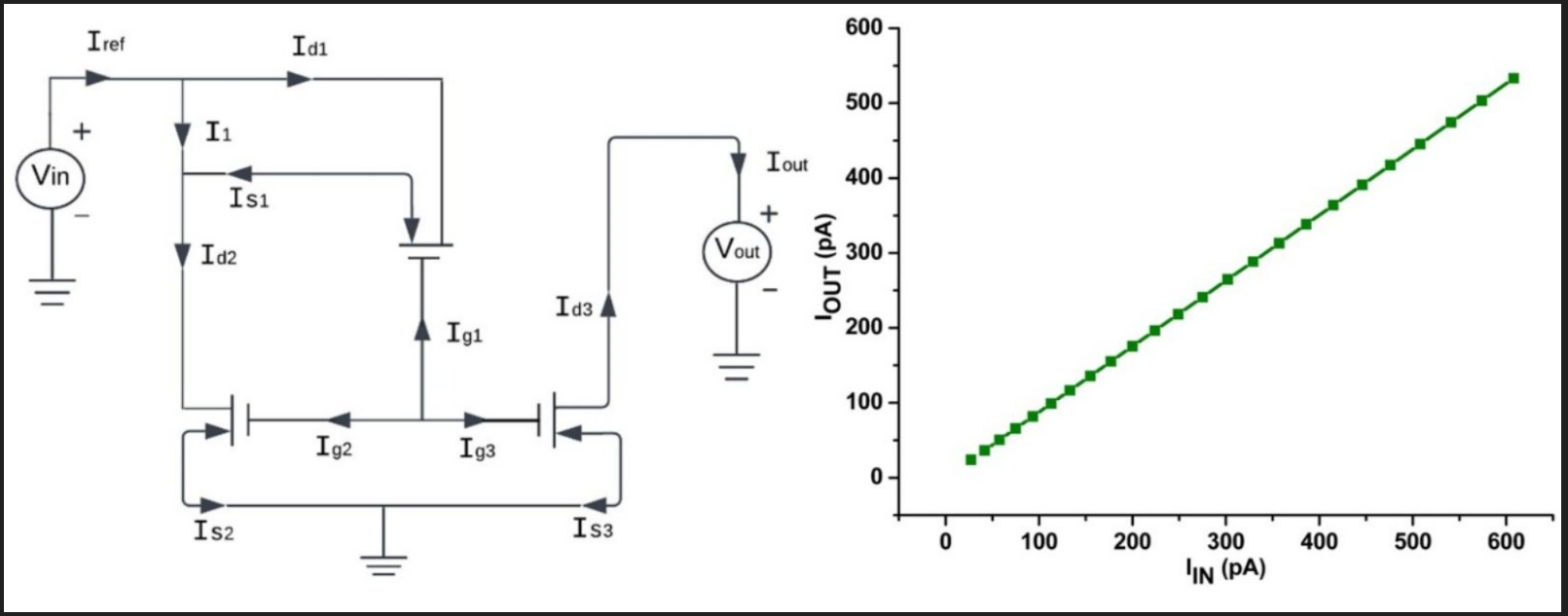
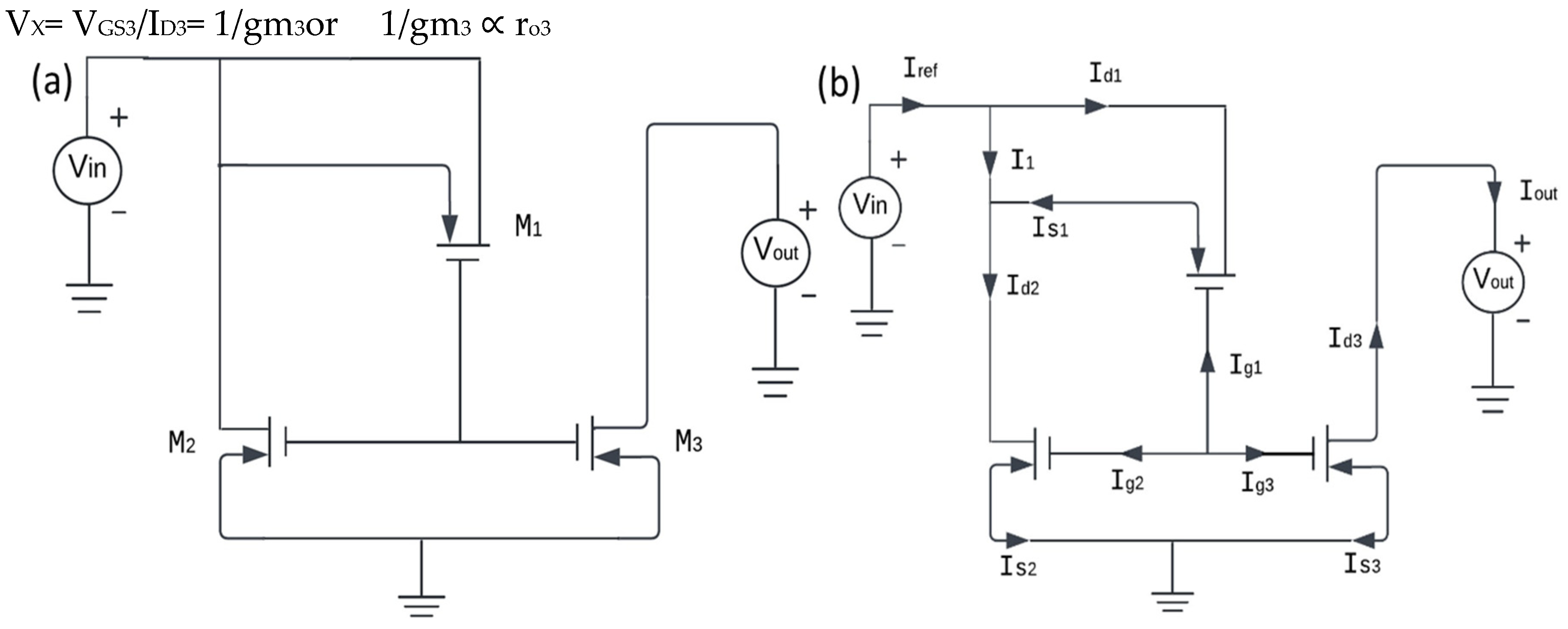
In this study, we present a novel current mirror (CM) circuit design. The circuit was designed to ensure precise current mirroring by applying the same voltage at both the input and output terminals, which is crucial for eliminating any voltage differentials that could potentially disrupt the accuracy of the mirroring process. By maintaining equal voltage levels across these terminals, the current replication at the output closely follows the reference current at the input, ensuring stable and consistent performance. This design choice not only optimizes current mirroring but also helps in achieving ultra-low current levels, crucial for high-precision applications. The configuration of the circuit is shown in Figure 1a, highlighting the placement and interaction of components that facilitate efficient operation. Through this arrangement, our CM circuit demonstrates high output impedance in the gigaohm (GΩ) range, low input impedance in the kiloohm (KΩ) range and stable output currents in the picoampere (pA) range, making it ideal for applications requiring ultra-low power consumption and high accuracy in current replication.
In this section, we explore the theoretical validation of the current mirroring effect and the output impedance of our proposed current mirror (CM) circuit. To verify the current mirroring effect, we aim to show that the output current matches the input current. Let the gate currents of MOSFETs M1, M2, and M3 be denoted as IG1, IG2, and IG3, and the drain currents as ID1, ID2, and ID3, while the source currents are represented as IS1, IS2, and IS3, respectively. Due to the high input impedance of MOSFET gates, negligible current (0.1 pA) flows into them (IG1 = IG2 = IG3 ≈ 0A) [16]. The input current, also known as the reference current, is denoted by IREF, and the output current by IOUT. Ideally, the output current in a CM should be equal to the reference current, and we aim to verify it in our design.
For this circuit, we also expect the output impedance to be extremely high, ideally infinite, to ensure that variations in output voltage do not affect the output current. To demonstrate this, consider that the output voltage at the drain of MOSFET M3 is VX. The transconductance of each MOSFET is denoted as gm. We define the output current IOUT= IS3, while Vg represents the common gate voltage for all the three MOSFETs.
In Figure 1b, the direction of the currents in the circuit is illustrated, showing how the reference current IREF is mirrored across MOSFET M3, resulting in an output current IOUT that closely matches the reference (Eq.1). This configuration ensures minimal voltage differential at the gate terminals, allowing precise current replication. After considering the channel effects and the transconductance, we confirm that the output impedance remains high, aligning with the theoretical expectations for an ideal current mirror (Eq.2). This analysis supports the practical results observed during simulations, validating both the accuracy of current mirroring and the high output impedance of our CM circuit design. To calculate the output current in terms of input current we assume that IG1 = IG2 = IG3 ≈ 0A [16].
Now to calculate the output impedance
IREF= I1 + ID1
ID3 = IS3
IS2 + IS3 = 0
IS3 = - IS2
ID3 = IOUT = - IS2 = - ID2
ID2 = IS1 + I1
ID2 = ID1 + I1 = IREF
IOUT = - IREF
ID3 = IS3
IS2 + IS3 = 0
IS3 = - IS2
ID3 = IOUT = - IS2 = - ID2
ID2 = IS1 + I1
ID2 = ID1 + I1 = IREF
IOUT = - IREF
VX = IX (1/gm3 + ro3)
Vx= Ix/gm3
Output Impedance = 1/gm3 = 1/ (ID3/VGS3)
Vx= Ix/gm3
Output Impedance = 1/gm3 = 1/ (ID3/VGS3)
Figure 1.
Circuit diagram of proposed current mirror: (a) without directions of current, (b) with directions of current.
Figure 1.
Circuit diagram of proposed current mirror: (a) without directions of current, (b) with directions of current.
4. Result and Discussion
We will now proceed to simulate our circuit using Cadence OrCAD X Capture software, focusing on the output and input voltages. Initially, we set a DC sweep of both the input and output voltages from 0 to 2V. As illustrated in Figure 2a, the graph clearly indicates a linear relationship between the output current and the input current, suggesting a consistent and predictable interaction between the two variables. This linear correlation is indicative of stable device performance within the analysed parameters, confirming the effectiveness of our current mirror design. The stability of the current mirror is crucial for various applications, particularly in integrated circuits, where accurate current mirroring is essential for maintaining performance and reducing power consumption. Moreover, this behaviour reinforces the design’s suitability for use in analog signal processing and precision measurement instruments, where even slight variations in current can lead to significant errors in system functionality [17].
To determine the output impedance of the circuit, the input terminal was provided with an input current half of the current range of the proposed device (500 pA), that is 250 pA in order to provide biasing to circuit while a DC voltage sweep from 0 to 2 V was applied to the output terminal. The output impedance, Rout, is calculated via ROUT = VOUT/IOUT. Figure 1b presents a graph depicting the relationship between output current and output voltage values, ranging from 0V to 2 V. From this analysis, we conclude that the stable output impedance of the device is approximately 20 GΩ, which is significantly high and ensures minimal loading effects when driving subsequent circuit stages [18]. Additionally, we found the output compliance voltage to be low as 0.9V, demonstrating the circuit’s capability to maintain a constant output current across varying load conditions with minimum input voltage. This performance is essential for applications that require stable current sources, especially in high-performance electronic systems, where fluctuations could lead to inaccurate readings and degraded performance. The high output impedance not only supports current mirroring but also enhances the device’s overall robustness in practical implementations, making it suitable for various scenarios requiring precision and reliability.
Now, to determine the input impedance of the circuit, the output terminal was grounded while a DC voltage sweep varies from 0 to 2V at the input terminal. The DC input impedance, RIN, is calculated via RIN = VIN/IIN. Figure 1c presents a graph depicting the relationship between input current and input voltage values, ranging from 0 to 2 V. From this analysis, we conclude that the stable input impedance of the device is approximately 2.735 kΩ, which is important for ensuring that the input stage does not significantly load the preceding circuit. The graph also illustrates a distinct behaviour of the device, defining an input compliance voltage of 0.8 V. Prior to this threshold, the device exhibits negligible change in input current with changes in input voltage. Once the compliance voltage of 0.8 V is reached, the device transitions into saturation mode, marking a departure from linear behaviour. Furthermore, we have plotted the error in current gain ((IOUT – IIN)/IIN) * 100 (in %) versus DC input voltage values ranging from 0 to 2 V, which can be observed in Figure 1d. The curve demonstrates a decreasing error rate as the input current increases, indicating that at higher input currents, the error diminishes significantly. Notably, after reaching an input current of 450 pA, the error stabilizes at 0.27438%, signifying that the input current has reached a saturation point. This performance highlights the effectiveness of our proposed current mirror circuit in accurately mirroring low currents while maintaining high impedance, making it essential for advanced applications in low-power and precision electronic systems. Ultimately, the results reinforce the viability of our circuit design for applications that demand both accuracy and reliability, setting a benchmark for future developments in current mirror technologies.
Figure 3a demonstrates the total power dissipation of the circuit, which stabilizes after 1.06 ns at a value of 8.39 µW. This stabilization after short period of time reflects the circuit’s efficiency in managing power consumption during operation. The low power dissipation is a critical aspect for applications requiring energy-efficient designs, especially in low-power electronics, where minimizing heat and energy loss is essential for maintaining device longevity and reducing operational costs [19]. Furthermore, the rapid stabilization of power dissipation ensures that the circuit reaches a steady state quickly, making it suitable for high-speed applications where transient power fluctuations could otherwise disrupt system performance. Figure 3b illustrates the AC current gain, which stabilizes at a value of 0.877 after reaching a frequency of 0.125 kHz. This stability in current gain ensures consistent amplification across the circuit’s operational bandwidth, highlighting the design’s robustness for analog signal processing tasks that require precise current control [20]. Figure 3c complements this by showing that the input impedance stabilizes at 3.643 kΩ after 93.75 kHz, indicating that the circuit maintains a predictable impedance across a wide frequency range, which is vital for minimizing signal distortion. Lastly, Figure 3d shows the relationship between input and output currents, both in pA, emphasizing the circuit’s capability to handle ultra-low current levels with high accuracy, making it well-suited for precision measurement applications in many advanced electronic systems. Also, the various performance parameters of the current mirrors reported in the previous research papers, along with the proposed current mirror, have been compiled and compared in Table 1.
5. Conclusion
In this paper, we have successfully demonstrated the design and performance of a current mirror using Cadence OrCAD X Capture software. Our simulations have confirmed a strong linear relationship between the input and output currents, indicative of stable and predictable operation, which is essential for precision applications. The high output impedance and low compliance voltage ensure minimal loading and stable current mirroring across varying conditions, making this design highly suitable for analog signal processing and precision measurement tasks. Furthermore, the analysis of power dissipation and current gain stability underscores the circuit’s efficiency and robustness, even in high-speed and low-power environments. The circuit’s ability to maintain consistent performance across different parameters, including low error rates and rapid stabilization of power dissipation, highlights its potential for use in advanced electronic systems requiring accuracy, reliability, and energy efficiency. Overall, our results validate the current mirror’s applicability in various high-performance scenarios, setting a strong foundation for future improvements and applications in low-power, precision electronics.
Notes
The authors declare no competing financial interest.
References
- Li, Y.; Wang, H.; Trik, M. Design and simulation of a new current mirror circuit with low power consumption and high performance and output impedance. Analog Integr Circuits Signal Process 2024, 119, 29–41. [Google Scholar] [CrossRef]
- Al-Absi, M.A. A novel highly accurate current mirror. International Journal of Electronics 2009, 96. [Google Scholar] [CrossRef]
- M. K. ; K. C. K. ; N. K. ; Atmakuri, C.M. Performance enhancement of flipped voltage follower current mirror in nanoscale technology. International Journal of Nano Dimension 2024, 15. [Google Scholar]
- Monfaredi, K.; Baghtash, H.F. An Extremely Low-Voltage and High-Compliance Current Mirror. Circuits Syst Signal Process 2020, 39, 30–53. [Google Scholar] [CrossRef]
- Tang, L.-S.; Huang, M.-H.; Kuo, P.-Y.; Yang, P.-H. Design of A Low Dropout Voltage Regulator Using Nested-Current-Mirror Rail-to-Rail-Output Single-Stage Amplifier. In Proceedings of the 2024 International Conference on Consumer Electronics - Taiwan (ICCE-Taiwan), Jul. 2024; IEEE; pp. 369–370. [Google Scholar] [CrossRef]
- Marani, R.; Perri, A.G. A Simulation Study of Noise Behavior in Basic Current Mirror using CNTFET and MOSFET. International Journal of Emerging Technology and Advanced Engineering 2021, 11, 13–18. [Google Scholar] [CrossRef] [PubMed]
- Pritty; Jhamb, M. A 0.8-Volt 29.52-μW Current Mirror-Based OTA Design for Biomedical Applications. Journal of Circuits, Systems and Computers 2023, 32. [Google Scholar] [CrossRef]
- Domala, N.; Sasikala, G. Low Power Low Voltage Current Mirror for Analog & Mixed Signal Applications. In Proceedings of the 2020 4th International Conference on Electronics, Communication and Aerospace Technology (ICECA), Nov. 2020; IEEE; pp. 465–470. [Google Scholar] [CrossRef]
- Domala, N.; Sasikala, G. Low Power Low Voltage Current Mirror for Analog & Mixed Signal Applications. In Proceedings of the 2020 4th International Conference on Electronics, Communication and Aerospace Technology (ICECA), Nov. 2020; IEEE; pp. 465–470. [Google Scholar] [CrossRef]
- Aggarwal, B.; Gupta, M.; Gupta, A.K. A comparative study of various current mirror configurations: Topologies and characteristics. Microelectronics J 2016, 53, 134–155. [Google Scholar] [CrossRef]
- Guran, I.-C.; Florescu, A.; Perisoara, L.A. A Novel Frequency Measurement Methodology for Clock Synchronization in SPICE-Based Simulators. IEEE Access 2023, 11, 117030–117039. [Google Scholar] [CrossRef]
- Guran, I.-C.; Florescu, A.; Perisoara, L.-A.; Vasile, A.; Oancea, C.-D. Fully Analog Clock Signal Generator for SPICE based simulators. In Proceedings of the 2022 14th International Conference on Electronics, Computers and Artificial Intelligence (ECAI), Jun. 2022; IEEE; p. 1. [Google Scholar] [CrossRef]
- Viman, L.; Chindris, G.; Pop, O. A new methodology for using OrCAD applications on a network. In Proceedings of the 24th International Spring Seminar on Electronics Technology. Concurrent Engineering in Electronic Packaging. ISSE 2001. Conference Proceedings (Cat. No.01EX492); IEEE; pp. 238–242. [CrossRef]
- Matousek, D.; Rejfek, L. Practical aspects of realisation of negative charge pumps. In Proceedings of the 2017 International Conference on Applied Electronics (AE), Sep. 2017; IEEE; p. 1. [Google Scholar] [CrossRef]
- Monfaredi, K.; Baghtash, H.F. An Extremely Low-Voltage and High-Compliance Current Mirror. Circuits Syst Signal Process 2020, 39, 30–53. [Google Scholar] [CrossRef]
- Chan, T.Y.; Chen, J.; Ko, P.K.; Hu, C. The impact of gate-induced drain leakage current on MOSFET scaling. In Proceedings of the 1987 International Electron Devices Meeting; IRE, 1987; pp. 718–721. [Google Scholar] [CrossRef]
- Yang, B.-D.; Shin, Y.-K.; Lee, J.-S.; Lee, Y.-K.; Ryu, K.-C. An accurate current reference using temperature and process compensation current mirror. In Proceedings of the 2009 IEEE Asian Solid-State Circuits Conference, Nov. 2009; IEEE; pp. 241–244. [Google Scholar] [CrossRef]
- Raguvaran, E.; Prasath, N.D.; Alexander, J.; Prithiviraj, N.; Santhanalakshmi, M. A very-high impedance current mirror for bio-medical applications. In Proceedings of the 2011 IEEE Recent Advances in Intelligent Computational Systems, Sep. 2011; IEEE; pp. 828–830. [Google Scholar] [CrossRef]
- Pritty; Jhamb, M. Ultra low power current mirror design with enhanced bandwidth. Microelectronics J 2021, 113, 105063. [Google Scholar] [CrossRef]
- Kawahito, S.; Tadokoro, Y. CMOS class-AB current mirrors for precision current-mode analog-signal-processing elements. IEEE Transactions on Circuits and Systems II: Analog and Digital Signal Processing 1996, 43, 843–845. [Google Scholar] [CrossRef]
- Chen, C.; Wu, X.; Yuan, X.; Zheng, X. A New Technique for the Subdomain Method in Predicting Electromagnetic Performance of Surface-Mounted Permanent Magnet Motors With Shaped Magnets and a Quasi-Regular Polygon Rotor Core. IEEE Transactions on Energy Conversion 2023, 38, 1396–1409. [Google Scholar] [CrossRef]
- Safari, L.; Minaei, S. A Low-Voltage Low-Power Resistor-Based Current Mirror and Its Applications. Journal of Circuits, Systems and Computers 2017, 26, 1750180. [Google Scholar] [CrossRef]
- Wang, G.; Wu, J.; Trik, M. A Novel Approach to Reduce Video Traffic Based on Understanding User Demand and D2D Communication in 5G Networks. IETE J Res 2024, 70, 5649–5665. [Google Scholar] [CrossRef]
- Yu, J.; et al. Synergistic piezoelectricity enhanced BaTiO3/polyacrylonitrile elastomer-based highly sensitive pressure sensor for intelligent sensing and posture recognition applications. Nano Res 2023, 16, 5490–5502. [Google Scholar] [CrossRef]
- Jindal, C.; Pandey, R. A high output resistance, wide bandwidth, and low input resistance current mirror using flipped voltage follower cell. International Journal of Circuit Theory and Applications 2021, 49, 3286–3301. [Google Scholar] [CrossRef]
Figure 2.
D.C. characteristics of proposed current mirror: (a) relationship between input current (IIN) and output current (IOUT), (b) relationship between output voltage (VOUT) and output current (IOUT), (c) relationship between input voltage (VIN) and input current (IIN) and (d) relationship between input current (IIN) and error (%).
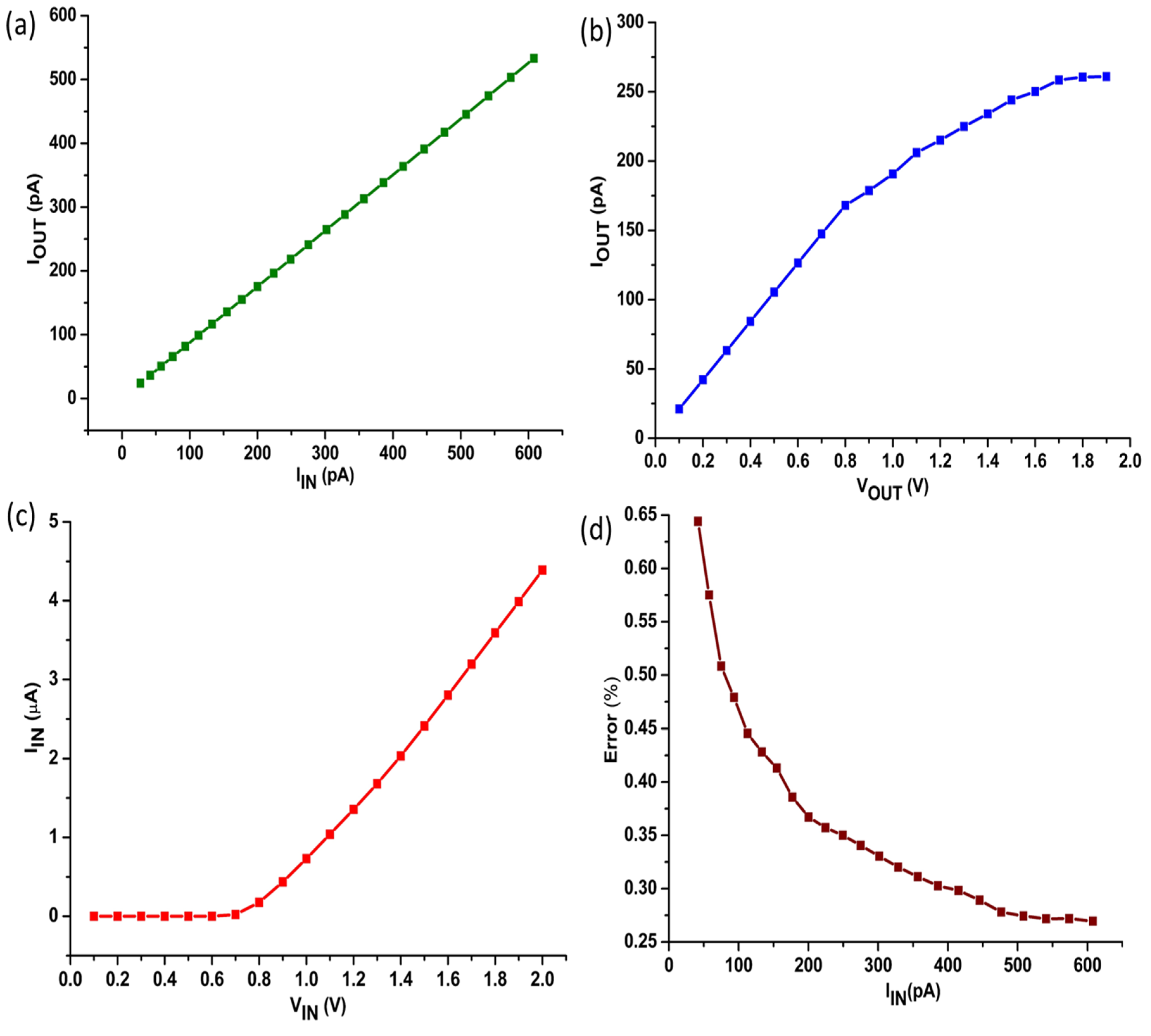
Figure 3.
A.C. characteristics of proposed current mirror: (a) relationship between time (ns) and power dissipation (µW), (b) relationship between frequency (Ghz) and A.C. current gain, (c) relationship between frequency (Ghz) and input impedance (kΩ) and (d) relationship between input current (IIN) and output current (IOUT).
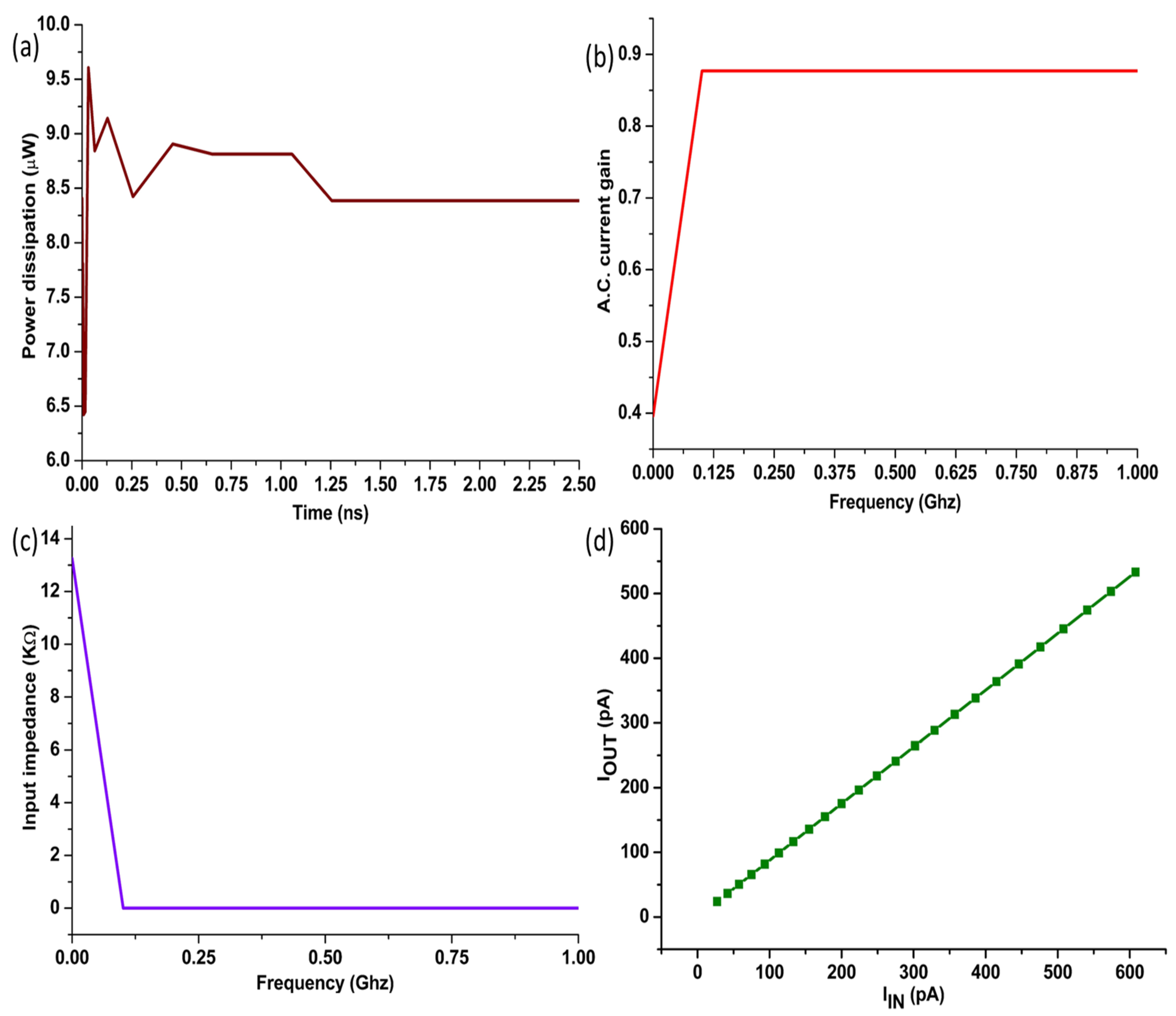

Table 1.
Comparison of different performance parameters of the proposed current mirror and current mirrors reported in the previous research papers.
Table 1.
Comparison of different performance parameters of the proposed current mirror and current mirrors reported in the previous research papers.
| Parameters | C. Chen et al. [21] | L. Safari et al. [22] | G. Wang et al. [23] | J. Yu et al. [24] | C. Jindal et al. [25] | This work |
| Current range (A) | 1 | 100 µ | NA | 0.7 | 300 µ | 500 p |
| Minimum input voltage (V) | 1.8 | 0.04 | 0.7 | 1.2 | 0.34 | 0.8 |
| Minimum output voltage (V) | 1.8 | 0.1 | NA | 91 m | 0.83 | 1.2 |
| Input resistance (Ω) | 6.4 | 496 | NA | 500 | 161.34 | 3.643 K |
| Output resistance (Ω) | 0.362 M | 1 M | NA | 1980 M | 19.83 G | 20 G |
| Power dissipation (μW) | 0.35 | 154 | 3.1 | 1.56 | 94 | 8.39 |
| Current transfer error (%) | 4 | 0.6 | 3 | 5 | 0.52 | 0.2743 |
Disclaimer/Publisher’s Note: The statements, opinions and data contained in all publications are solely those of the individual author(s) and contributor(s) and not of MDPI and/or the editor(s). MDPI and/or the editor(s) disclaim responsibility for any injury to people or property resulting from any ideas, methods, instructions or products referred to in the content. |
© 2024 by the authors. Licensee MDPI, Basel, Switzerland. This article is an open access article distributed under the terms and conditions of the Creative Commons Attribution (CC BY) license (http://creativecommons.org/licenses/by/4.0/).
Copyright: This open access article is published under a Creative Commons CC BY 4.0 license, which permit the free download, distribution, and reuse, provided that the author and preprint are cited in any reuse.


