Preprint
Article

This version is not peer-reviewed.

Performance Analysis of Scandium-Doped Aluminum Nitride-Based PMUTs Under High-Temperature Conditions

A peer-reviewed article of this preprint also exists.

Submitted:

09 December 2024

Posted:

10 December 2024

You are already at the latest version

Abstract

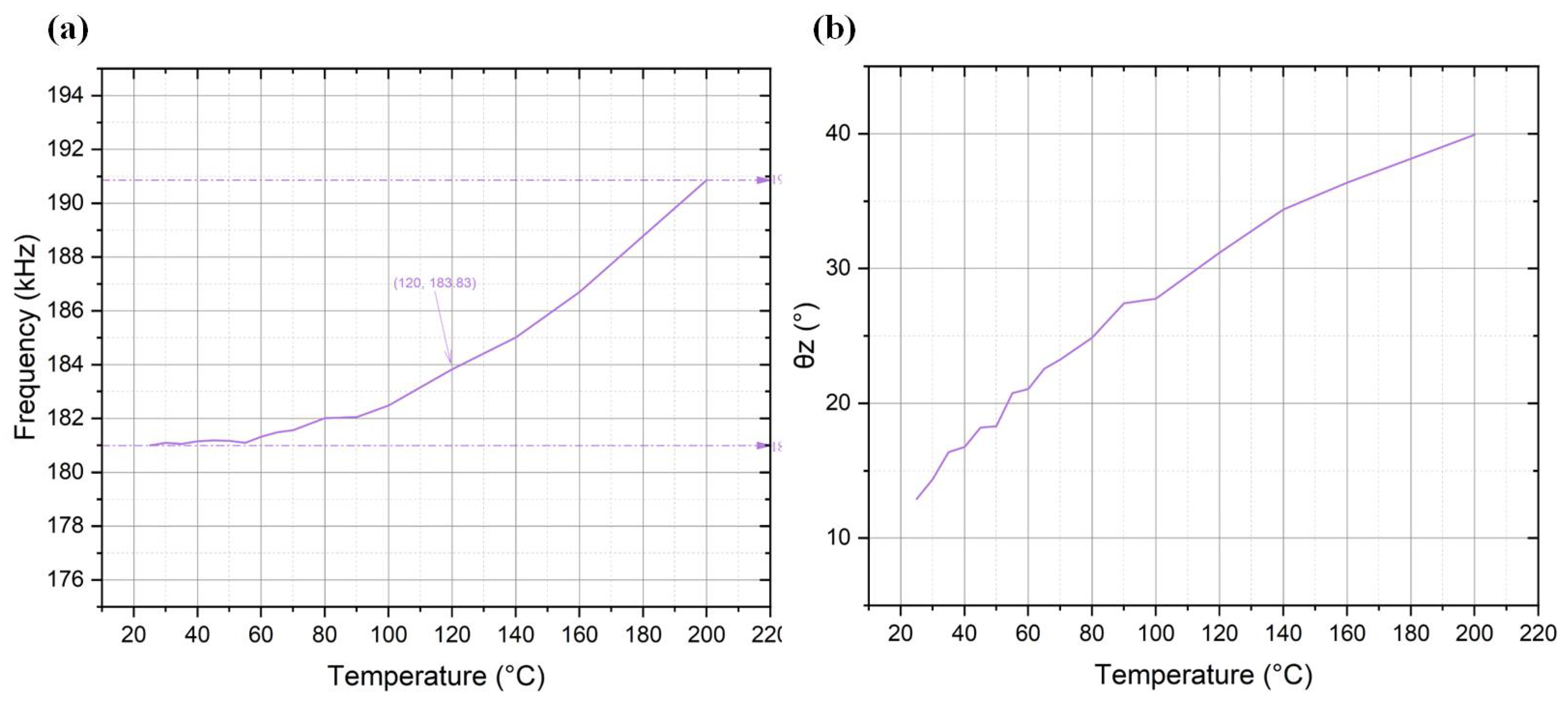
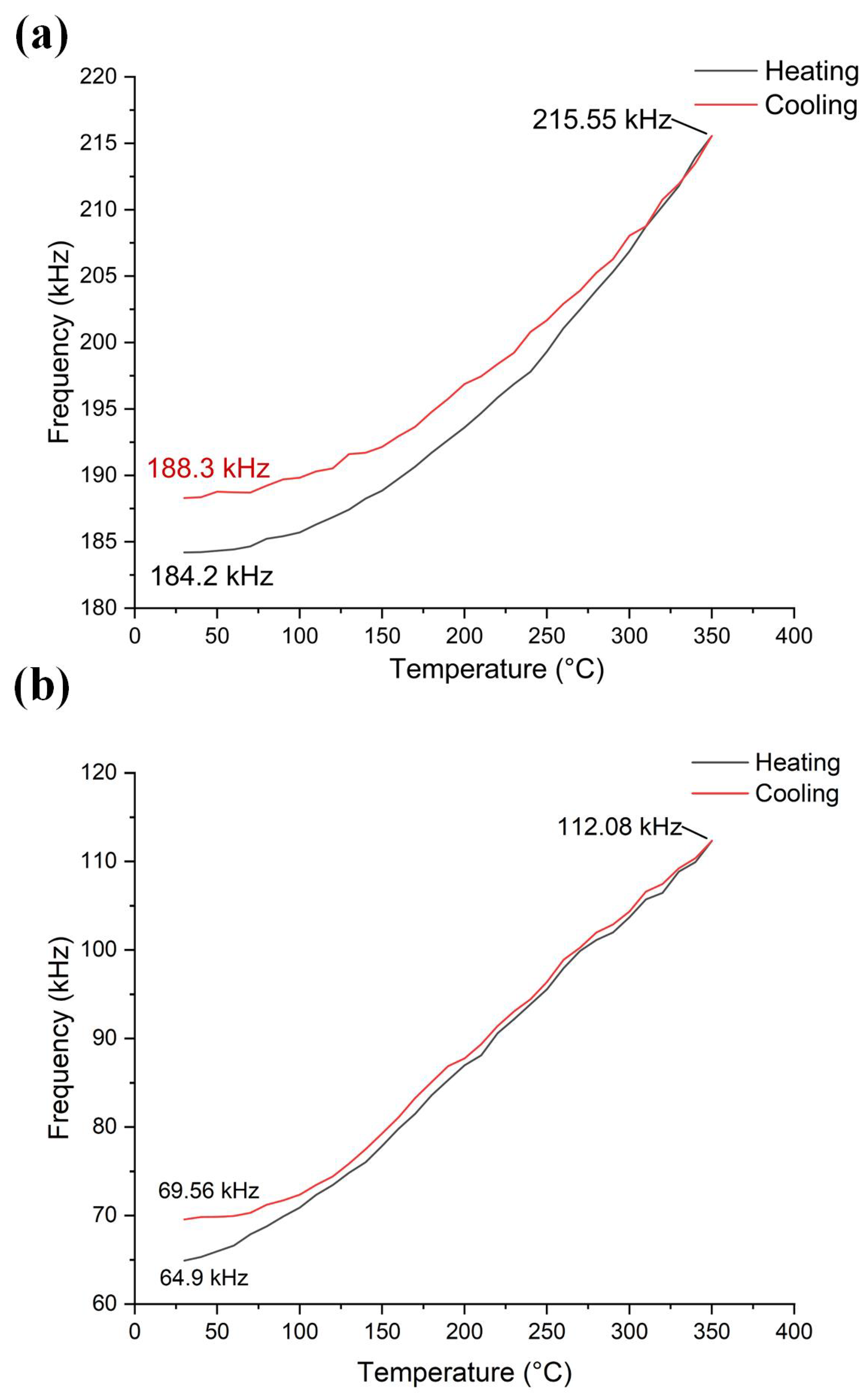
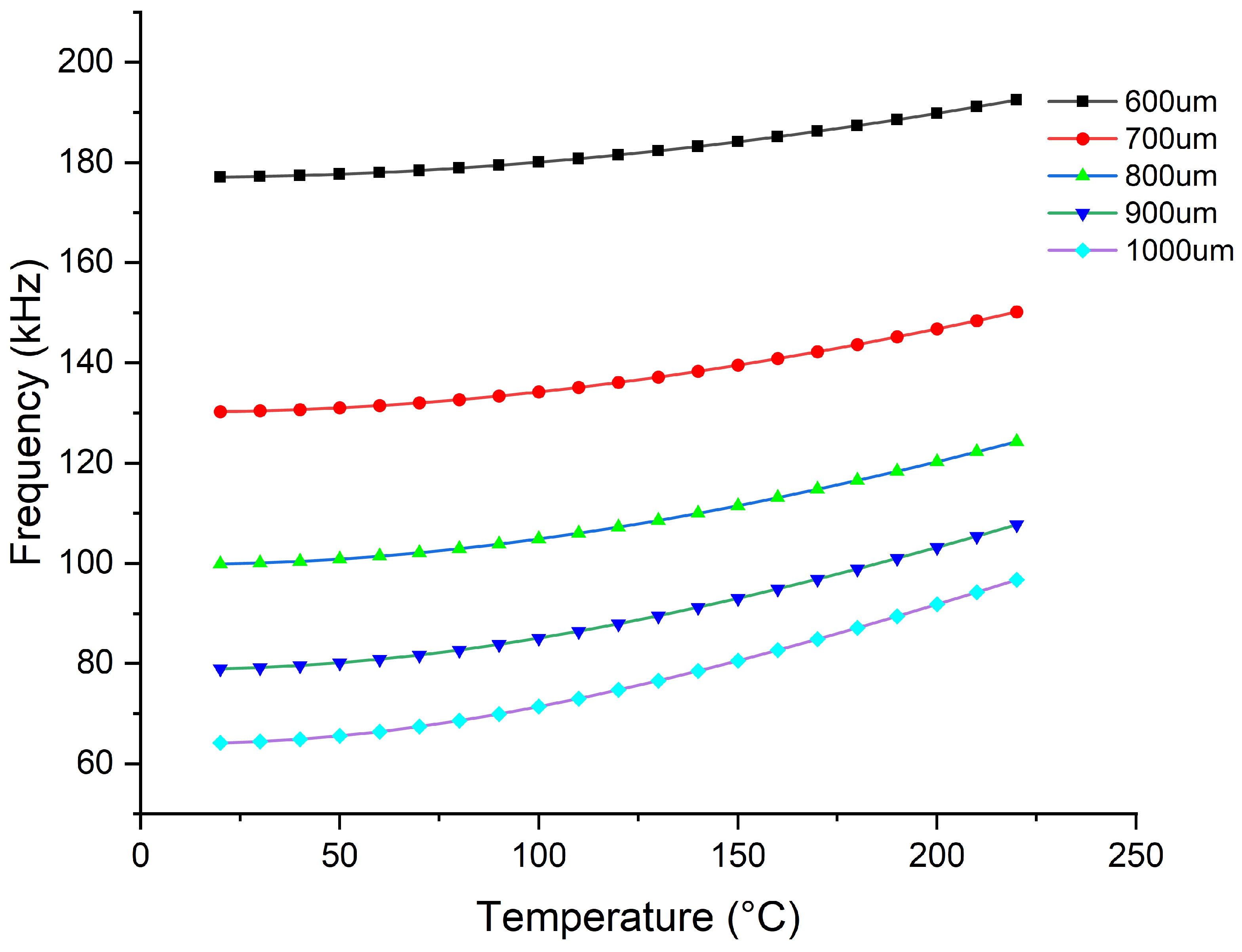
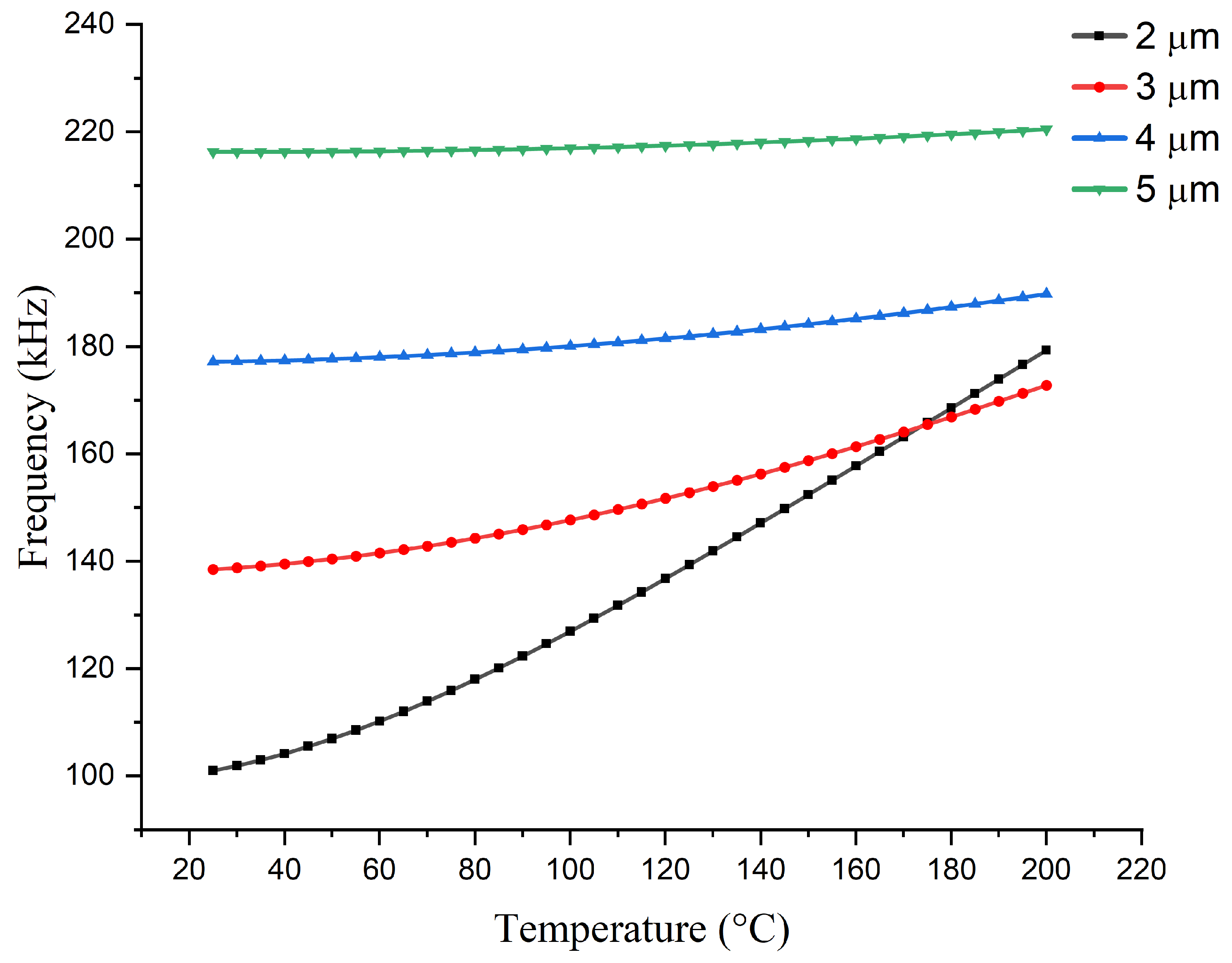
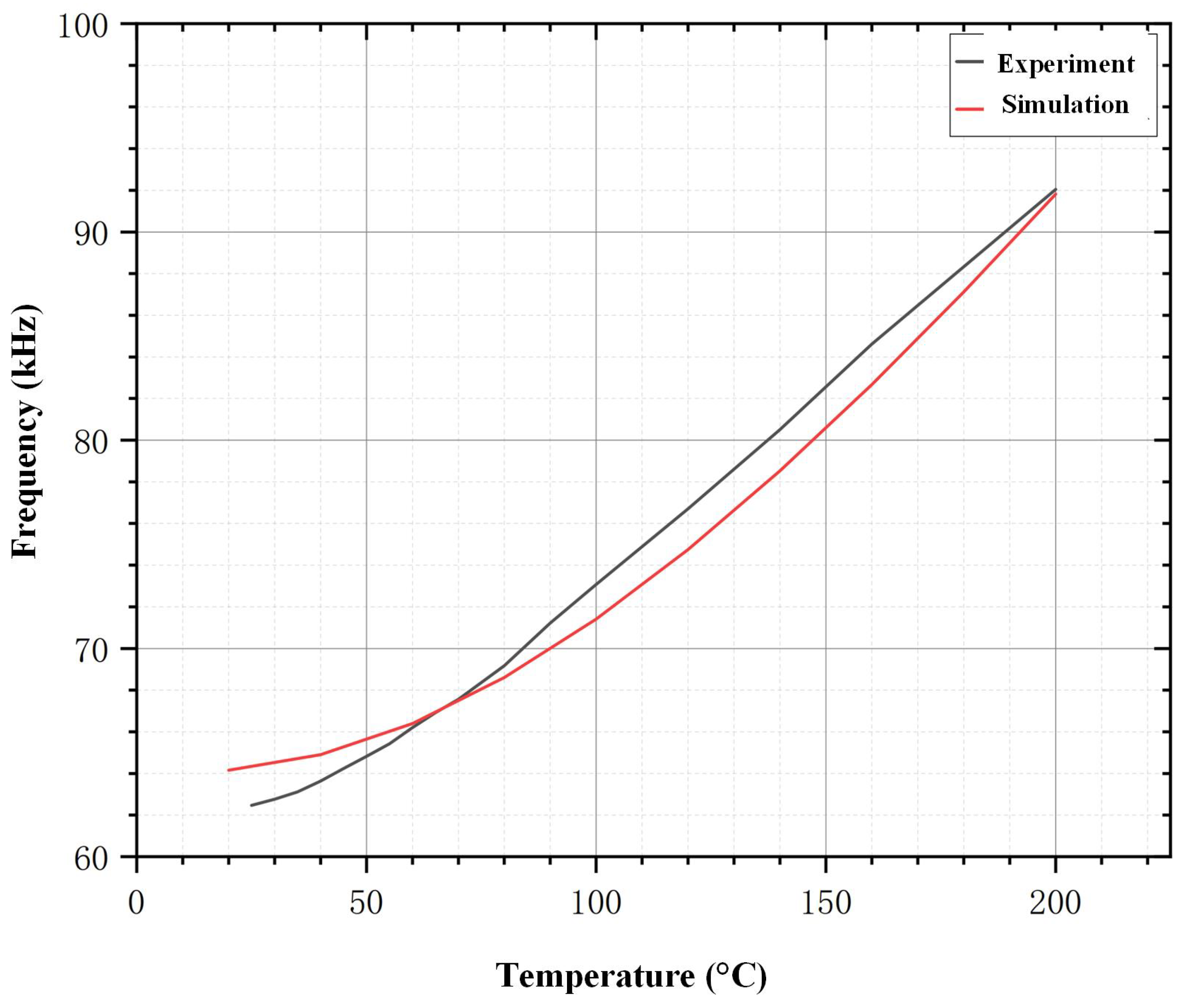
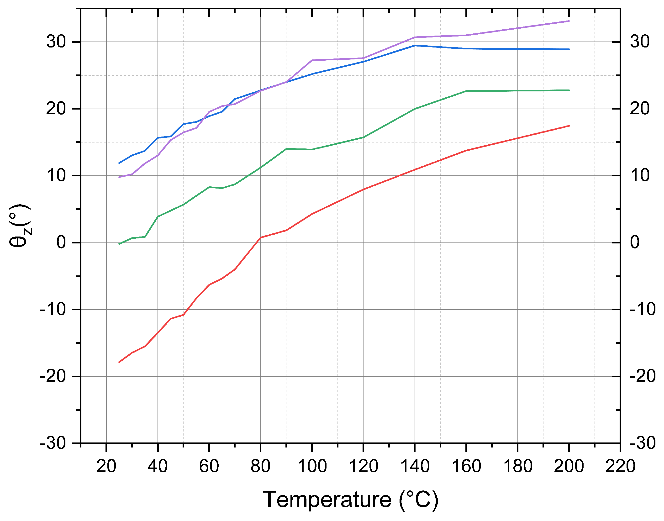
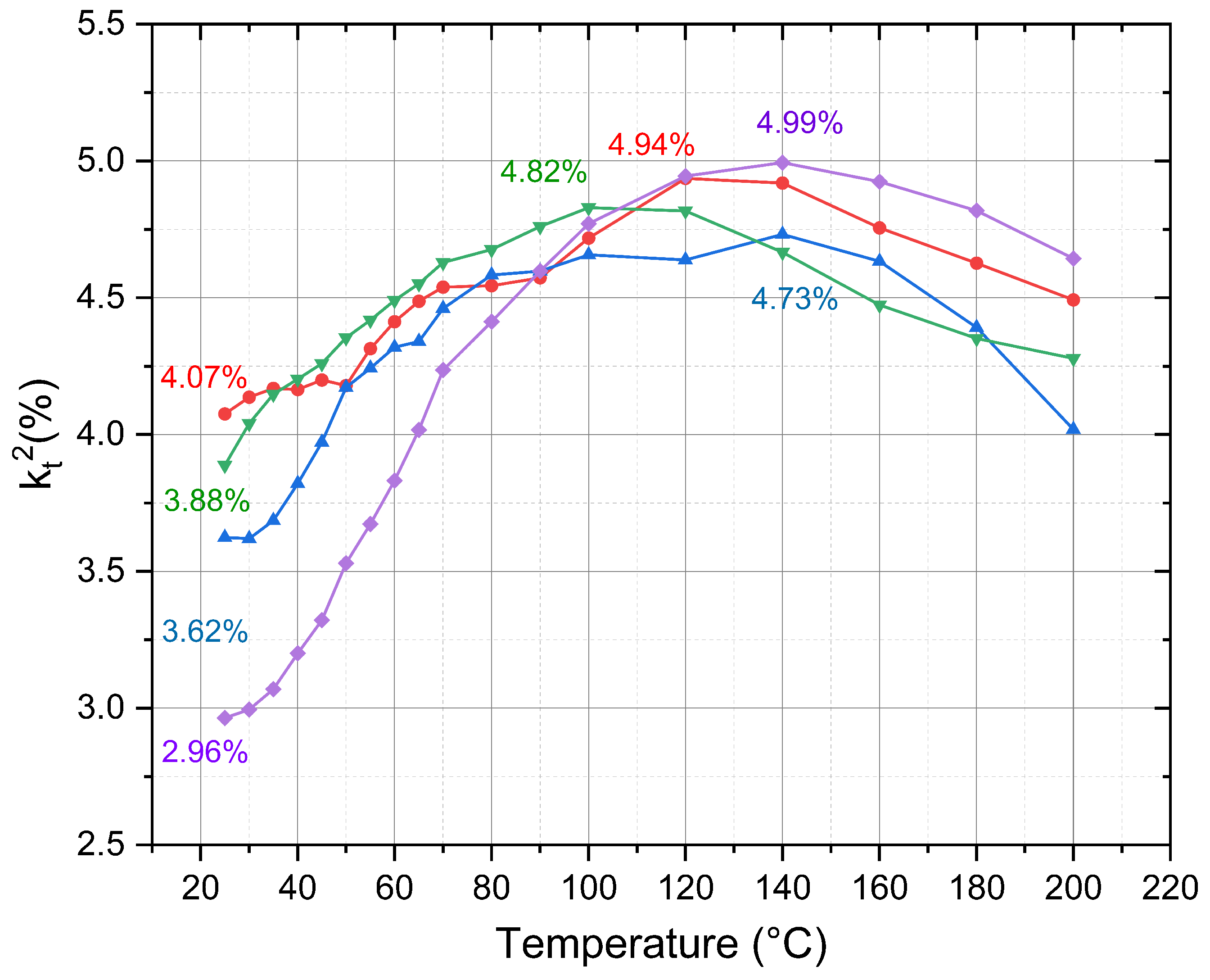
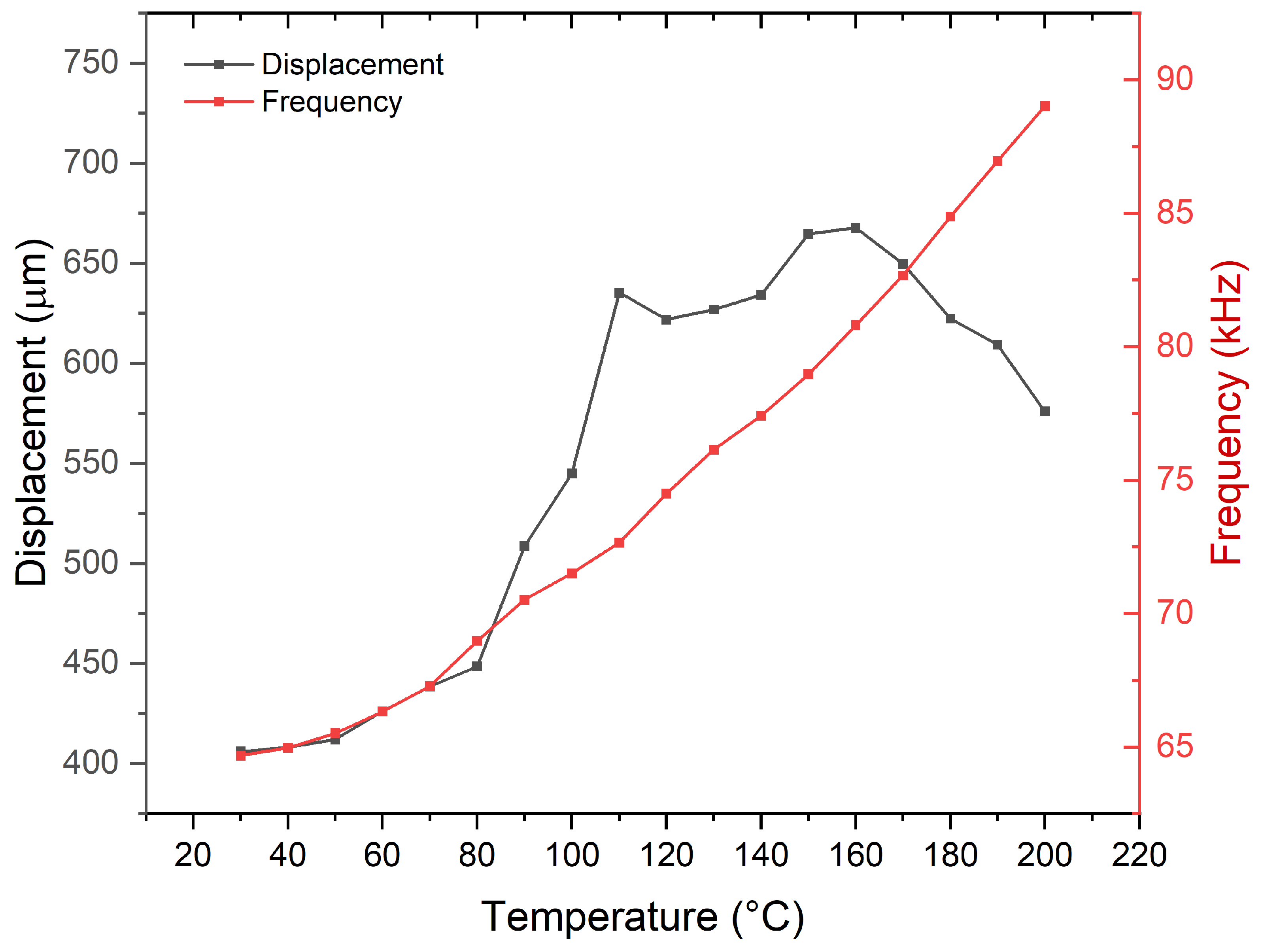
This paper investigates the performance of scandium-doped aluminum nitride (AlScN) piezoelectric micromachined ultrasonic transducers (PMUTs) under extreme high-temperature conditions. Key findings include significant warpage due to thermal expansion, increasing from 0.306 µm at room temperature to 1.823 µm at 150°C. Resonant frequency showed a linear drift, with frequency shifts reaching 44\% at 200°C. The impedance phase increased from -41.56° at room temperature to +2.45° at 200°C, and the electromechanical coupling coefficient rose to between 21.4\% and 68.6\% in the temperature range of 100°C to 140°C. High-temperature cycling also revealed irreversible frequency shifts, indicating lasting thermal effects on device integrity. These results provide crucial insights into the behavior of AlScN-based PMUTs in harsh environments, guiding their design and reliability evaluation for high-temperature applications.

Keywords: 
;  ;  

1. Introduction

Sensors are at the heart of modern scientific and technological progress, driving advancements in information technology beyond computation and communication, and enabling "perception" and "intelligence." The increasing demand for intelligent sensors is reflected in the proliferation of smart applications, including autonomous vehicles, smart homes, and smart cities.
Micro-Electro-Mechanical Systems (MEMS) technology plays a key role in enabling intelligent sensors by integrating sensing and actuation at the microscale through semiconductor micro- and nanofabrication processes. MEMS sensors achieve conversion between various physical quantities, mechanical vibrations, and electrical signals through structural design. Their small size, low power consumption, high reliability, and ease of integration make MEMS sensors particularly advantageous for applications requiring miniaturization and intelligent functionality [1].
Among piezoelectric materials used for MEMS sensors, aluminum nitride (AlN) and scandium-doped AlN (AlScN) have attracted considerable attention due to their compatibility with CMOS processes. AlN-based sensors have found rapid industrial development in RF MEMS [2,3], optical MEMS [4,5], and acoustic MEMS applications [6,7]. Acoustic MEMS, specifically micromachined ultrasonic transducers (MUTs), have become a major area of focus due to their potential for smart and portable applications [8,9].
Traditional bulk ceramic ultrasonic transducers, primarily made from sintered PZT-based piezoelectric ceramics, have significant drawbacks. Their relatively large size, high power consumption, and manufacturing inconsistencies make them unsuitable for modern smart applications [10,11,12]. Compared to these traditional transducers, MEMS-based ultrasonic sensors, such as AlN piezoelectric micromachined ultrasonic transducers (PMUTs), offer substantial advantages, including smaller size, lower power consumption, and improved integrability with CMOS technology. These benefits make PMUTs particularly suitable for portable devices, medical ultrasound imaging, and gesture recognition applications [13,14,15,16,17].
A major advantage of AlN-based MEMS sensors is their ability to operate under high-temperature conditions. Traditional PZT-based piezoelectric sensors exhibit reduced piezoelectric performance at elevated temperatures, due to thermal effects that affect electric dipole alignment [18]. In contrast, AlN, with its stable wurtzite crystal structure and lack of a Curie temperature, maintains good piezoelectric performance even at high temperatures, making it suitable for use in harsh environments [19].
Despite the advantages of AlN-based PMUTs, research on their performance under high-temperature environments remains limited [20]. Although AlN has demonstrated good high-temperature stability as a piezoelectric material, a systematic study on the performance of AlN PMUTs, particularly concerning resonant frequency, electromechanical coupling, and stress variations under high-temperature conditions, is lacking. This gap in the literature presents a significant opportunity for understanding the reliability and optimization of PMUTs in harsh environments.
In this work, we address this gap by investigating the high-temperature performance of AlN PMUTs fabricated using standard SOI processes. This study aims to evaluate the changes in performance parameters such as resonance frequency and electromechanical coupling under elevated temperatures, thereby contributing to the understanding of PMUT reliability and optimization for applications in harsh environments.

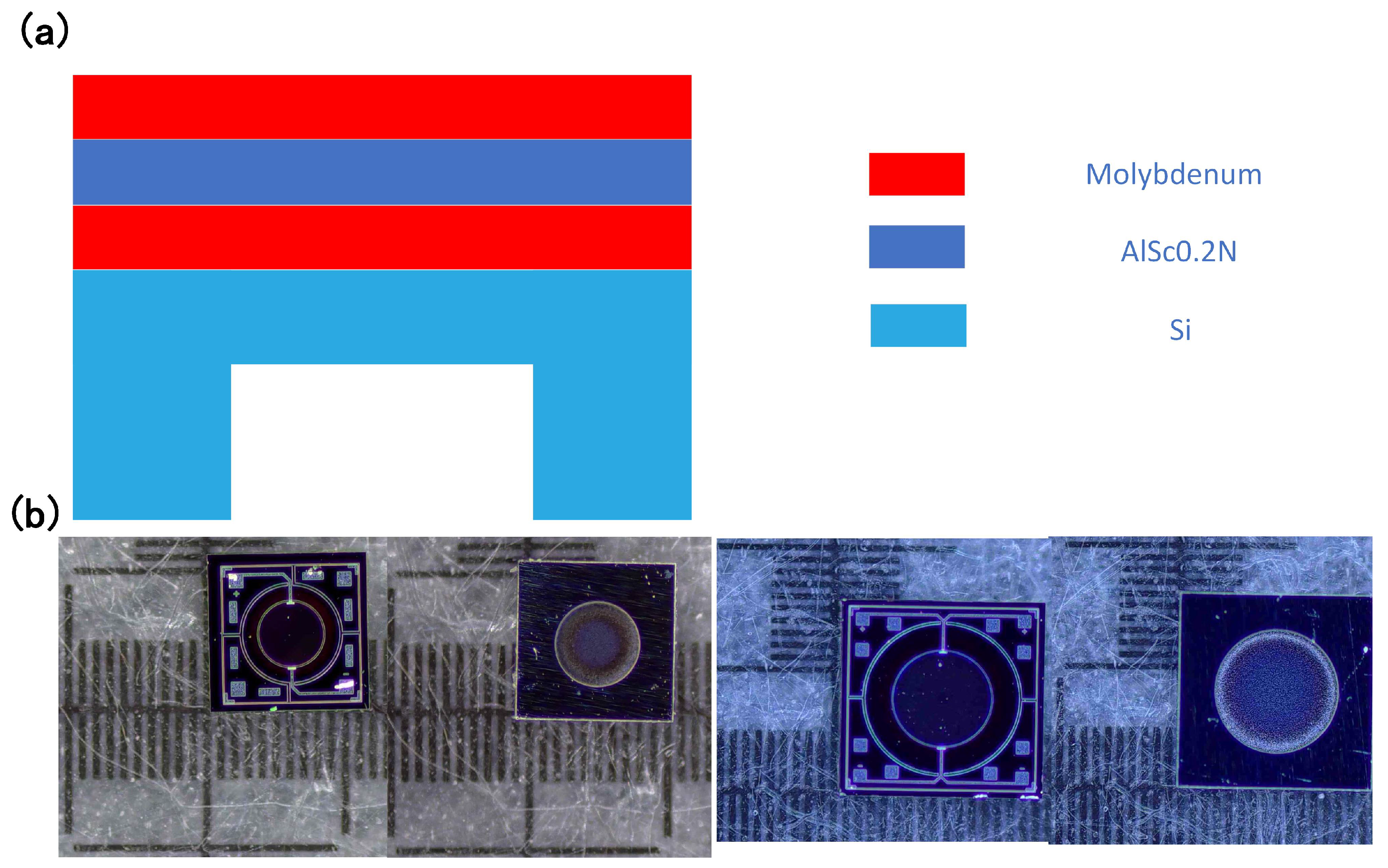
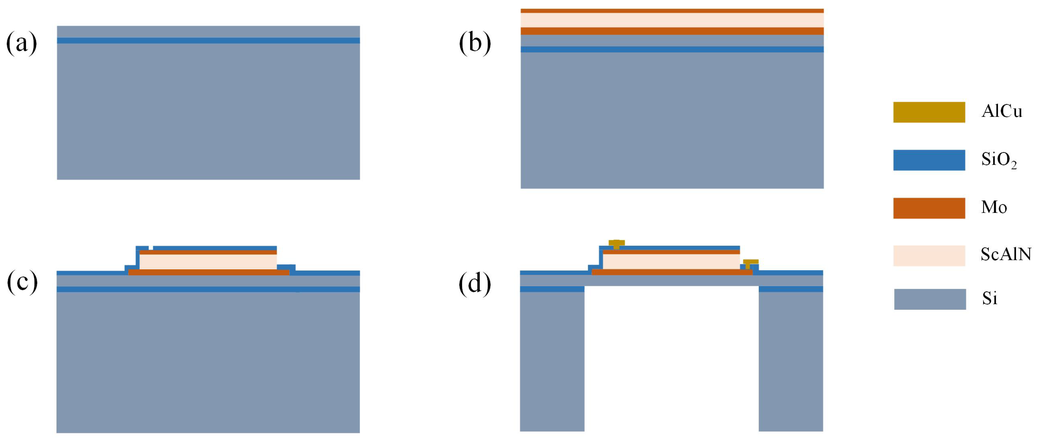
2. Device and Methodology

The devices used in this study are shown in Figure 1. Figure 1a illustrates the schematic structure of the device. The piezoelectric layer is aluminum nitride (AlN) doped with 20% scandium, with a thickness of 1 μ m. Mo electrodes are placed on both sides of the piezoelectric layer, and the bottom structural layer is silicon 4 μ m. The diameters of the back cavity of the PMUTs used in this study are 600 μ m and 1000 μ m, respectively. Physical images of the front and back sides of these two sizes are shown in Figure 1b. The diameter of the piezoelectric layer is designed as 78% of the diameter of the back cavity, following previous work [21] .
The PMUT fabrication process in this paper follows the standard SOI (Silicon-On-Insulator) manufacturing process, as shown in Figure 2. On an SOI box wafer with a top silicon layer thickness of 4 μ m, the bottom Mo electrode, scandium-doped aluminum nitride, and top Mo electrode are sequentially deposited. Subsequently, the aforementioned three-layer structure is patterned to form vias, followed by AlCu deposition for metallization. Finally, the back cavity is etched, forming the structure shown in Figure 2d. The device dimensions and core material parameters used in this study are shwon in Table 1. [22].
The impact of varying structural parameters on the temperature characteristics of SOI-based PMUTs was analyzed using finite element analysis (FEA). The FEA focused on three key parameters: the diameter of the back cavity and the thickness of the top silicon layer. These parameters are also critical to determine the final resonant frequency of the device. The material properties used in the FEA are listed in Table 2, including the mechanical and electrical properties of the Molybdenum electrodes, piezoelectric layer, and silicon.
Figure 1. (a) Schematic diagram of the device structure (b) Front and back images of two PMUTs with different back cavity sizes
Preprints 142399 g001
Table 1. Dimensions of the proposed PMUTs
Parameter Dimension
Top Mo electrode diameter 468/780
Membrane diameter 600/1000
Top Mo electrode thickness 0.1
ScAlN piezoelectric layer thickness 1
Bottom Mo electrode thickness 0.2
Seed layer thickness 0.05
Si structural layer thickness 4
Figure 2. Process flow of the device
Preprints 142399 g002
Table 2. Properties of the Materials for PMUT FEM
Property Mo ScAlN Si
Dielectric permittivity 13.7
Density (kg/m³) 10200 3560 2320
Young’s Modulus (GPa) 312 230 130
C 11 = C 12 (GPa) 325
C 33 (GPa) 279
C 13 (GPa) 131
C 44 = C 55 (GPa) 99
C 66 (GPa) 94
d 31 (pm/V) -4
d 33 (pm/V) 9.9
The FEA results of the effect of temperature on the frequency of the device under varying diameters of the back cavity are presented in Figure 3. When the diameter of the back cavity diameter is 600 μ m, the resonant frequency of the device changes from 177.08 kHz at room temperature to 189.79 kHz, corresponding to a variation of 7. 17%. As the diameter of the back cavity increases, the frequency shift rate increases, reaching 12.6% at 700 μ m, 20.4% at 800 μ m, 30.6% at 900 μ m, and ultimately 43.1% at 1000 μ m. The back cavity primarily affects the stiffness of the device, influencing its temperature stability. To mitigate frequency shifts as a result of temperature variation, the reduction of the back cavity size should be considered to enhance the device’s temperature stability.
The effect of varying the thickness of the top silicon layer on the temperature stability of the device is shown in Figure 4. As the thickness of the silicon layer increases, the temperature stability changes significantly. When the thickness of silicon above is 2 μ m, the frequency change rate due to temperature reaches 77.2%, while it is only 1.9% at 5 μ m. The results indicate that, at higher temperatures, the frequency shift exhibits a nearly linear trend, and as the device stiffness decreases (i.e., with decreasing silicon thickness), this linear slope increases. Future experiments will further validate this observed trend.

3. Experiment and Result

To verify the reliability of the simulation results aforementioned, we selected a device with a silicon top thickness of 4 μ m and a back cavity diameter of 1000 μ m, whose initial resonant frequency at room temperature closely matches the simulation results. The device was placed in a cascade probe station equipped with a heating function and the positive and negative electrodes of the device were directly connected to the E4990A impedance analyzer using probes. The probe stage was heated in increments of ten degrees and the changes in the resonant frequency were recorded. The variation in resonant frequency with temperature for this design was also calculated using FEM, and both results are compared in Figure 5. The comparison shows that the experimental results agree well with the simulation in both numerical values and trends, demonstrating the reliability of the simulation for the design of devices related to temperature drift.
Four devices with a diameter of the back cavity of 1000 μ m were selected from the fabricated 8-inch wafer for further investigation. The heating and testing method for the devices is as described above.
Figure 6 shows the change in resonant frequency with temperature for the four devices. The initial frequency differences among the four devices were mainly caused by processing errors and differences in residual stress. In the figure, all devices show a similar trend of resonant frequency change with temperature, and the results are summarized in Table 3. From room temperature to 80°C, the frequency of the devices exhibited a slow upward trend, with a frequency drift ranging from 7.5% to 11% at 80 ° C. As the temperature increased further to 200 ° C, the frequency drift showed a roughly linear trend. A linear fit of the high-temperature range of the resonant frequency for the four devices revealed slopes between 0.186 and 0.19, and at 200°C, the frequency drift exceeded 44% compared to the initial frequency.
The impedance phase angles of the four devices were analyzed, and the results are shown in Figure 7. The impedance phase angles of all four devices increased with increasing temperature, with the largest change observed in a device whose impedance phase increased from -18.56° at room temperature to +17.45 ° at 200 ° C. The electromechanical coupling coefficient of the four devices was also analyzed using
k t 2 = C m C m + C 0 = π 2 4 f s f p f s f p .
for electromechanical coupling coefficient, and the results are shown in Figure 8. Figure 8 indicates that the electromechanical coupling coefficient of the four PMUTs initially increases with temperature and then decreases. Compared to room temperature, the electromechanical coupling coefficient increased by 21.4% to 68.6%, reaching its maximum around 100 ° C to 140 ° C.
To further explore the influence of temperature on PMUTs based on scandium-doped AlN SOI, the aforementioned tests were repeated with devices having a back cavity diameter of 600 μ m. The piezoelectric layer and the top silicon thickness were the same as those of the previous devices. The frequency and impedance phase changes with temperature are shown in Figure 10. The frequency change with temperature follows a similar trend, with a slow increase at lower temperatures followed by a roughly linear change at higher temperatures. At 200°C, the frequency increased from 181 kHz to 190.86 kHz, resulting in a frequency drift of 5.45%. The impedance phase also increased with temperature, changing from 12.9 at room temperature to 39.9 at 200 ° C. In addition, comparing the experimental results of the devices with back cavity sizes of 600 μ m and 1000 μ m with the simulation results mentioned above, it can be observed that the trends are generally consistent, confirming that increasing back cavity size affects the sensitivity to temperature drift of the device.
In addition, to validate the conclusion of the simulation on the effect of the top silicon thickness on the device, an experiment was carried out using devices with different top silicon thicknesses, while other structural parameters were kept the same, with a back cavity size of 600 μ m. The results are shown in Figure 9. The experimental results indicate that devices with a top silicon thickness of 3 to 5 μ m follow the trend of the simulation results, demonstrating that temperature drift is more pronounced when the top silicon is thinner. Similarly, when the top silicon thickness is smaller, the slope of the temperature drift change, appearing as a nearly linear interval at higher temperatures, is also significantly larger, which is consistent with the FEM analysis results.
Figure 9. Frequency variation with temperature for devices with a 600 μ m back cavity with different top Si thickness.
Preprints 142399 g009
Figure 10. Frequency and impedance phase variation with temperature for devices with a 600 μ m back cavity.
Preprints 142399 g010
To investigate the macroscopic morphological changes of the devices under temperature influence, heating was performed using a heating plate due to limitations of the 3D profilometer. Two devices with a back cavity of 600 μ m and two devices with a back cavity of 1000 μ m were placed on a soft bottom heating plate, and the entire setup was placed under the 3D profilometer to characterize device warpage. The heating plate was heated to 50 ° C, 100 ° C and 150 ° C, and the warpage results are shown in Table 3. The results indicate that with increasing temperature, thermal expansion caused an increase in residual stress, leading to increased warpage of the devices, which in turn contributed to frequency drift and affected other performance parameters.
Table 4. Warpage variation of the devices with temperature (room temperature, 50°C, 100°C, and 150°C).
Device Initial Wrap( μ m) Wrap at 50°C ( μ m) Wrap at 100°C ( μ m) Wrap at 150°C ( μ m)
600 μ m No. 1 0.20 0.34 0.55 0.87
600 μ m No. 2 0.21 0.36 0.57 0.93
1000 μ m No. 1 0.19 0.58 1.12 1.83
1000 μ m No. 2 0.3 0.71 1.24 2.15
To further explore the performance of the devices at high temperatures, a Polytech MSA 600 laser Doppler vibrometer (LDV) was used to characterize the mechanical vibration frequency and amplitude of the devices at different temperatures, with the results shown in Figure 11. The frequency change trend obtained from the LDV tests was consistent with that from electrical characterization, while the amplitude showed an initial increase followed by a decrease. The amplitude increased from 402.6 μ m at room temperature to 668.7 μ m at 160°C, representing an increase of 66.1%. This trend was also consistent with the change in the electromechanical coupling coefficient obtained from electrical characterization, further demonstrating that the PMUT exhibits good electromechanical coupling performance at higher temperatures.
To investigate the repeatability of the devices after they were operated at high temperatures, a heating-cooling cycling experiment was conducted, and the change in the resonant frequency of the devices was characterized. Both types of devices were slowly heated to 350 ° C and then slowly cooled to room temperature, with measurements taken every 10 ° C. The results are shown in Figure 12. The experiment revealed that both types of devices exhibited changes in the initial resonant frequency after the experiment returned to room temperature. When the resonant frequency of both devices was measured again after 24, 48, and 72 hours, it was found that the frequency had not returned to its original value, indicating that PMUTs based on scandium-doped aluminum nitride experience performance changes after operating at high temperatures, which are difficult to recover in the short term.
A 3D profilometer was used to characterize the devices in the different states. However, because of the very small frequency deviation, only slight changes were observed, making it impossible to determine whether the changes were due to the effect of the high temperature or the measurement error. Therefore, these results are not detailed in this paper.
Figure 12. Resonant frequency variation during heating and cooling cycles for devices with different back cavity sizes: (a) 600 μ m and (b) 1000 μ m.
Preprints 142399 g012

4. Conclusions

This study demonstrates that both the back cavity size and the top silicon thickness significantly affect the temperature drift characteristics of SOI-based air-coupled PMUTs. The FEM simulations and experimental results consistently show that larger back cavity sizes and thinner top silicon layers lead to increased temperature drift. The PMUT with a diameter of the back cavity of 1000 μ m and a thickness of the top silicon of 4 μ m exhibited a high temperature drift rate of 47.3% as the temperature increased from room temperature to 200 ° C. Furthermore, elevated temperatures enhanced the electromechanical coupling coefficient and mechanical amplitude, indicating improved performance metrics despite increased warpage. The findings contribute to a deeper understanding of the behavior of PMUT in high-temperature environments and provide essential theoretical insights for optimizing PMUT design for high-temperature applications.

Author Contributions

Conceptualization, H.L. methodology, H.L.; writing—original draft preparation, A.S.; writing—review and editing. All authors have read and agreed to the published version of the manuscript.

Funding

This research was funded by Gleen Hawatt Electro-Ceramic Lab.

References

  1. Algamili, A.S.; Khir, M.H.M.; Dennis, J.O.; Ahmed, A.Y.; Alabsi, S.S.; Ba Hashwan, S.S.; Junaid, M.M. A Review of Actuation and Sensing Mechanisms in MEMS-Based Sensor Devices. Nanoscale Research Letters 2021, 16, 16. [CrossRef]
  2. Mahameed, R.; Sinha, N.; Pisani, M.B.; Piazza, G. Dual-beam actuation of piezoelectric AlN RF MEMS switches monolithically integrated with AlN contour-mode resonators. Journal of Micromechanics and Microengineering 2008, 18, 105011. [CrossRef]
  3. Fernandez-Bolanos Badia, M.; Buitrago, E.; Ionescu, A.M. RF MEMS Shunt Capacitive Switches Using AlN Compared to $\hbox{Si}_{3}\hbox{N}_{4}$ Dielectric. Journal of Microelectromechanical Systems 2012, 21, 1229–1240. [CrossRef]
  4. Ruotsalainen, K.; Morits, D.; Ylivaara, O.M.E.; Kyynäräinen, J. Resonating AlN-thin film MEMS mirror with digital control. Journal of Optical Microsystems 2022, 2. [CrossRef]
  5. Lei, H.; Wen, Q.; Yu, F.; Li, D.; Shang, Z.; Huang, J.; Wen, Z. AlN film based piezoelectric large-aperture MEMS scanning micromirror integrated with angle sensors. Journal of Micromechanics and Microengineering 2018, 28, 115012. [CrossRef]
  6. Segovia-Fernandez, J.; Sonmezoglu, S.; Block, S.T.; Kusano, Y.; Tsai, J.M.; Amirtharajah, R.; Horsley, D.A. Monolithic piezoelectric Aluminum Nitride MEMS-CMOS microphone. In Proceedings of the 2017 19th International Conference on Solid-State Sensors, Actuators and Microsystems (TRANSDUCERS). IEEE, 6 2017, pp. 414–417. [CrossRef]
  7. Fei, C.; Liu, X.; Zhu, B.; Li, D.; Yang, X.; Yang, Y.; Zhou, Q. AlN piezoelectric thin films for energy harvesting and acoustic devices. Nano Energy 2018, 51, 146–161. [CrossRef]
  8. Roy, K.; Lee, J.E.Y.; Lee, C. Thin-film PMUTs: a review of over 40 years of research, 2023. [CrossRef]
  9. Akhbari, S.; Sammoura, F.; Shelton, S.; Yang, C.; Horsley, D.; Lin, L. Highly responsive curved aluminum nitride pMUT. In Proceedings of the 2014 IEEE 27th International Conference on Micro Electro Mechanical Systems (MEMS). IEEE, 1 2014, pp. 124–127. [CrossRef]
  10. Sun, S.; Wang, J.; Ning, Y.; Zhang, M. Air-coupled piezoelectric micromachined ultrasonic transducers for surface stain detection and imaging. Nanotechnology and Precision Engineering 2022, 5. [CrossRef]
  11. Karuthedath, C.B.; Sebastian, A.T.; Saarilahti, J.; Sillanpaa, T.; Pensala, T. Design and Fabrication of Aluminum Nitride Piezoelectric Micromachined Ultrasonic Transducers for Air Flow Measurements. In Proceedings of the 2019 IEEE International Ultrasonics Symposium (IUS), 2019, pp. 2489–2492. [CrossRef]
  12. Sammoura, F.; Akhbari, S.; Lin, L.; Kim, S.G. Enhanced coupling of piezoelectric micromachined ultrasonic transducers with initial static deflection. In Proceedings of the SENSORS, 2013 IEEE, 2013, pp. 1–4. [CrossRef]
  13. Akhbari, S.; Sammoura, F.; Eovino, B.; Yang, C.; Lin, L. Bimorph Piezoelectric Micromachined Ultrasonic Transducers. Journal of Microelectromechanical Systems 2016, 25, 326–336. [CrossRef]
  14. Su, J.; Fichtner, S.; Ghori, M.Z.; Wolff, N.; Islam, M.R.; Lotnyk, A.; Kaden, D.; Niekiel, F.; Kienle, L.; Wagner, B.; et al. Growth of Highly c-Axis Oriented AlScN Films on Commercial Substrates. Micromachines 2022, 13, 783. [CrossRef]
  15. Sadeghpour, S.; Joshi, S.V.; Wang, C.; Kraft, M. Novel Phased Array Piezoelectric Micromachined Ultrasound Transducers (pMUTs) for Medical Imaging. IEEE Open Journal of Ultrasonics, Ferroelectrics, and Frequency Control 2022, 2, 194–202. [CrossRef]
  16. Savoia, A.S.; Casavola, M.; Boni, E.; Ferrera, M.; Prelini, C.; Tortoli, P.; Giusti, D.; Quaglia, F. Design, Fabrication, Characterization, and System Integration of a 1-D PMUT Array for Medical Ultrasound Imaging. In Proceedings of the 2021 IEEE International Ultrasonics Symposium (IUS). IEEE, 9 2021, pp. 1–3. [CrossRef]
  17. Hardy, E.; Fain, B.; Mesquida, T.; Blard, F.; Gardien, F.; Rummens, F.; Bastien, J.; Chatroux, J.; Martin, S.; Rat, V.; et al. Spike-based Beamforming using pMUT Arrays for Ultra-Low Power Gesture Recognition. In Proceedings of the 2022 International Electron Devices Meeting (IEDM). IEEE, 12 2022, pp. 1–24. [CrossRef]
  18. Gubinyi, Z.; Batur, C.; Sayir, A.; Dynys, F. Electrical properties of PZT piezoelectric ceramic at high temperatures. Journal of Electroceramics 2008, 20, 95–105. [CrossRef]
  19. Maiwa, H.; Kim, S.H.; Ichinose, N. Temperature dependence of the electrical and electromechanical properties of lead zirconate titanate thin films. Applied Physics Letters 2003, 83, 4396–4398. [CrossRef]
  20. Esteves, G.; Habermehl, S.D.; Clews, P.J.; Fritch, C.; Griffin, B.A. AlN/SiC MEMS for High-Temperature Applications. Journal of Microelectromechanical Systems 2019, 28, 859–864. [CrossRef]
  21. Liang, Y.; Eovino, B.E.; Lin, L. Pinned Boundary Piezoelectric Micromachined Ultrasonic Transducers. In Proceedings of the 2019 IEEE 32nd International Conference on Micro Electro Mechanical Systems (MEMS). IEEE, 1 2019, pp. 791–794. [CrossRef]
  22. Lyu, H.; Xiu, X.; Zhang, S.; Yang, H.; Safari, A. Piezoelectric Micromachined Ultrasonic Transducers under Forced Vibration: Improving Acoustic Range and Reducing Blind Area. IEEE Sensors Journal 2024, pp. 1–1. [CrossRef]
Figure 3. Frequency variation with temperature for devices with different back cavity sizes (FEM).
Preprints 142399 g003
Figure 4. Frequency variation with temperature for devices with different Si thickness (FEM).
Preprints 142399 g004
Figure 5. FEA and Experiment result comparison of the PMUT with 1000 μ m back cavity
Preprints 142399 g005
Figure 6. Frequency characteristics of four devices with a back cavity size of 1000 μ m as temperature changes.
Preprints 142399 g006
Figure 7. Impedance phase variation of four devices with temperature.
Preprints 142399 g007
Figure 8. Variation of electromechanical coupling coefficient of the devices with temperature.
Preprints 142399 g008
Figure 11. Amplitude and mechanical resonant frequency variation with temperature for devices with a 1000 μ m back cavity (LDV test results).
Preprints 142399 g011
Table 3. Frequency characteristics of four devices as temperature changes.
Initial Frequency
(kHz)
Frequency Drift
80°C (kHz)
Frequency Drift percentage
80°C
Frequency Drift 200°C (kHz) Frequency Drift percentage
200°C
Linearity
62.73 69.6 0.11 92.39 0.473 0.19
62.46 69.17 0.107 92.03 0.473 0.19
61.07 65.68 0.075 88 0.441 0.186
59.55 64.25 0.079 86.86 0.459 0.188
Disclaimer/Publisher’s Note: The statements, opinions and data contained in all publications are solely those of the individual author(s) and contributor(s) and not of MDPI and/or the editor(s). MDPI and/or the editor(s) disclaim responsibility for any injury to people or property resulting from any ideas, methods, instructions or products referred to in the content.
Copyright: This open access article is published under a Creative Commons CC BY 4.0 license, which permit the free download, distribution, and reuse, provided that the author and preprint are cited in any reuse.
Prerpints.org logo

Preprints.org is a free preprint server supported by MDPI in Basel, Switzerland.

Subscribe

Disclaimer

Terms of Use

Privacy Policy

Privacy Settings

© 2025 MDPI (Basel, Switzerland) unless otherwise stated