
Submitted:
04 December 2024
Posted:
05 December 2024
You are already at the latest version
Abstract
Signal conditioning circuits, in particle energy spectrum determination systems, introduce shaping characteristics that affect pulse integrity. This study explores algorithms to compensate for these effects, focusing on a digital signal processing for pole-zero cancellation (PZC) and unfolding techniques. The PZC algorithm successfully corrects baseline shift and pulse amplitude loss, providing significant improvements in signal fidelity. An unfolding is then applied for fine-tuning the compensation, further enhancing the recovery of the signal. Implemented on FPGA, the algorithms enable real-time compensation for various signal conditioning circuits, demonstrating enhanced performance across different experimental conditions.
Keywords:
signal conditioning
; digital signal processing
; inverse problems
; FPGA implementation
; high-energy calorimetry
1. Introduction
Pulse detectors are essential measuring instruments in high-energy physics, astronomy, and nuclear physics, among others. They can interact with short-duration phenomena, such as particle interactions, and provide corresponding electrical pulses, albeit with low electrical charge. These pulses, while small in magnitude, carry crucial information about the energy of the interacting particles, contributing to the energy spectrum determination, which is key for precise analysis and understanding of the underlying physical processes.
The instrumentation of these detectors involves pulse conditioning circuits and an Analog-to-Digital Converter (ADC), as illustrated in Figure 1. The conditioning circuits shape the signal to mitigate noise and optimize it for digitization [1], while the ADC converts the conditioned signal into a digital format suitable for storage and detailed computational analysis.
These devices often employ scintillators optically coupled to photomultipliers sensors, with the Silicon PhotoMultipliers (SiPMs) being a widely adopted choices [2,3]. The emergence of SiPMs in many recent detection systems is driven by their advantages, such as compactness, low operating voltage, and high sensitivity to light. However, this widespread adoption comes with the need for careful signal processing, as their inherent noise [4]. Connected to the SiPMs, the Charge-Sensitive Preamplifiers (CSP) plays a crucial role in front-end readout system to collect the charge generated by the photodetector and convert it into a voltage signal with amplitudes suitable for the acquisition system [5]. Nonetheless, these components introduce additional noise [6].
The combined noise from these sources, along with other potential contributors, poses a significant challenge in energy spectrum measurements, where precise determination of the time-of-flight and the pulse amplitude are essential for accurately estimating the particle interaction energy. To address the noise challenges, filtering techniques by the pulse shaper circuit (PSC) are employed [3].
The typical and simplest configuration of a PSC is the CR-nRC, consisting of a high-pass filter stage followed by n low-pass filter stages [1,7]. This configuration also handles the intrinsic waveform characteristics of SiPM-based detectors, characterized by extremely short rise and fall times (on the order of a few nanoseconds). The increased dynamic range requirements of these waveforms pose significant challenges for digitization in digital processing approaches without prior analog conditioning, as they demand high sampling rates that are often technologically challenging or economically impractical, especially in multi-channel systems. However, the signal conditioning process not only enhances the signal-to-noise ratio but also stretches the pulse duration. This pulse stretching effectively reduces the required sampling rate, alleviating the technological constraints on the acquisition system.
An undesired effect that can arise from pulse stretching is signal pileup, which is also influenced by the event rate. High event rates combined with wide pulse shapes significantly increase the probability of pileup. Such pileup distorts the measured amplitude, deviating it from the true signal amplitude, as presented in Figure 2. When the event rate is known, the SC can be designed to balance the need for pulse extension to reduce noise with the requirement to minimize pileup.
Another strategy to mitigate pileup involves the use of a high-pass filter, which narrows the output pulse widths, thereby decreasing the pileup probability. However, high-pass filters force the pulse average to zero, introducing negative components into the signal. The accumulation of these negative components leads to an undershooting effect with potentially long time constants, resulting in tail pileup and causing a baseline shift, as presented in Figure 3 [8]. Inevitably, a coupling capacitor is required in the signal conditioning circuit to block the high supply voltage of the photomultiplier from reaching the readout chain, effectively functioning as a high-pass filter.
Baseline shift can be mitigated by incorporating a parallel resistor with the coupling capacitor to achieve pole-zero cancellation (PZC) [8]. Regarding pulse width, reducing it before digitization impacts the design of the digitization system. A potential approach is to maintain a wide pulse with a optimal time constant to reduce noise, while avoiding additional high-pass filtering stages. This highlights the trade-off in analog processing: it can effectively reduce noise and correct baseline shift but does not address pileup, leaving it as an untreated effect.
PSCs are traditionally implemented through analog approaches, have increasingly been adapted to digital implementations using high-speed digitizers in specific applications [9,10,11]. Digital signal processing offers several advantages, including the ability to implement advanced filtering functions that are impractical in analog circuits, ease of parameter adjustments, adaptive filtering, and efficient correction of baselineshift and pileup effects [1,12]. Consequently, a hybrid approach that leverages both analog and digital processing provides a compelling solution for balancing performance, complexity, and cost in modern detection systems.
In digital processing, deconvolution, or unfolding, algorithms as described by Jordanov [13,14], Difulvio [12], Zeng [15], Födisch [16] and Stezelberger [17], are highly efficient at canceling modal components, enabling both pulse narrowing and undershooting reduction. Consequently, the larger pulse width required for digitization is no longer a limitation, as it can be narrowed post-digitization, effectively mitigating pileup, restoring the original signal characteristics. Furthermore, the traditional analog approach, using a resistor is unnecessary, since a digitally implemented unfolding PZC algorithm performs this task efficiently while offering the advantage of online adjustment.
According to Jordanov [18], implementing a stable digital PZC algorithm requires resetting the internal states of its feedback circuitry upon the arrival of new pulses. This limitation makes PZC unsuitable for high pileup environments. One of the goals of this work is to propose an adaptive control mechanism for the internal state variables, preventing baseline divergence and enabling the use of PZC in environments with high signal pileup.
This work, therefore, proposes a hybrid approach that combines analog processing for initial adjustment of pulse amplitude and duration, as well as noise treatment, with digital processing implemented on an FPGA to enable streaming operation. This hybrid strategy addresses both undershooting and pileup, leveraging the strengths of each processing domain.
As a proof of concept, the Monte Carlo simulation by Lorenzetti [19] is employed to model a scintillator detector with approximately 10,000 channels. The system operates under varying event rates to evaluate the performance of the readout channels in simulated experimental conditions. This evaluation primarily focuses on the acquisition system’s ability to handle pileup and undershooting at high event rates. These conditions are particularly relevant for experiments such as the IceCube Neutrino Observatory [20], ATLAS [21], and CMS [22] at the HL-LHC and FCC [23]. Other notable examples include the Compressed Baryonic Matter (CBM) experiment at the Facility for Antiproton and Ion Research (FAIR)[24], Hyper-Kamiokande[25], and similar studies.
The simulated readout setup consists of a scintillator optically coupled to a SiPM, with the resulting pulses processed by a CSP and a CR-4RC shaper circuit. While effective, this configuration introduces additional challenges in pulse analysis due to the modifications imposed by the signal processing stage. These challenges have motivated the development and application of the unfolding method, which will be detailed in the subsequent sections.
2. Materials and Methods
This section describes the environment and methodology employed to generate the data sets, as well as depicts the proposed signal processing strategies used for performance evaluation.
2.1. Detector Simulation
A stand-alone tool, part of the Lorenzetti Simulator [19], was utilized to generate the energy deposits within a generic calorimeter [26]readout system. The Lorenzetti Simulator is a versatile framework designed to support novel signal reconstruction and triggering strategies, and it was specifically employed to produce the simulated samples used in this study. The Lorenzetti engine facilitates developments at the signal processing chain level, enabling the assessment of advanced signal processing approaches for modern calorimetry and triggering systems. For event generation, Lorenzetti integrates Pythia 8 [27], while event propagation is handled by Geant4 [28,29,30], a widely adopted framework in fields such as high-energy physics, nuclear physics, accelerator physics, medical science, and space science. Geant4 serves as a primary tool for simulating particle interactions with matter using Monte Carlo methods [31].
2.1.1. Data Events Generation
In this work, 2,000,000 sequential particle collisions were simulated for different event-rate conditions. The event rate, measured in events per unit time, is a critical parameter in detector systems as it reflects the frequency at which interactions or signals are generated.
The considered events rates conditions ranges from 1% to 70%, representing a wide spectrum from very low to relatively high interaction frequencies. The specific intervals were chosen to provide a comprehensive analysis of system performance across different regimes. Lower rates (1% to 10%) allow the system to be tested in conditions where pulses are well-separated, ensuring minimal pileup and baseline interference. High rates (20% to 70%) simulate high-frequency conditions where pileup and baseline shift become significant challenges, stressing the limits of the readout and signal processing system.
The event rates were selected to align with a natural logarithmic scale (1%, 2%, 3%, 5%, 7%, 10%, 20%, 30%, 50%, 70%), which is particularly useful for systems where performance spans several orders of magnitude and ensures uniform representation across the range, avoiding excessive clustering of values in one region. This approach also provides sensitivity to changes in lower rates, where small variations can have a significant impact on performance, while efficiently analyzing higher rates with fewer points. The analysis captures system behavior across the desired range without requiring an excessively dense sampling, while focusing on regions of interest, particularly those where event rates introduce significant challenges in terms of pileup and baseline stability.
2.1.2. Convolutional Model
In this work, we present the modeling of a detection system based on a scintillator detector with SiPMs, where the system input is modeled as a radiation pulse, and the equivalent electronic circuit consists of a charge-sensitive preamplifier followed by a PSC based on a CR-4RC filter. The goal is to analyze the system’s response to these signals and study the characteristics of the pulse after particle interaction with the SiPM, as well as its electronic conversion and processing.
a. Input Electrical Pulse
The pulse modeling first considers the system input as an impulse generated by the particle interaction with the scintillator material, which is converted into an electrical signal by the SiPM. Scintillator detectors produce a temporal light response when particles interact with the material. This response is characterized by a rapid rise in light intensity, followed by an exponential decay due to the scintillation process [32,33,34]. The capacitive properties of SiPMs further shape the signal through charge accumulation and discharge, which can also be described by exponential functions [35,36]. As a result, the sensor output can be accurately modeled using a multi-exponential function that captures the light pulse’s rise and decay phases along with the associated electrical processes [37]. For practical purposes, however, the electrical pulse is approximated by a bi-exponential function, presented in equation:
where is the incident intensity, is the decay time of the pulse, and is the rise time of the pulse.
Represented in Laplace domain by:
b. Charge Sensitive Preamplifier
The signal generated by the SiPM is then amplified by a CSP, presented in Figure 4, whose role is to convert the accumulated charge into a voltage , that the peak amplitude is proportional to the number of detected photons and preserving the energy information deposited in the detector [38,39]. Calculating the CSP transfer function , presented in equation 3, is essential to model the circuit’s response to an input current , enabling precise reconstruction of the output signal and ensuring accurate energy measurements.
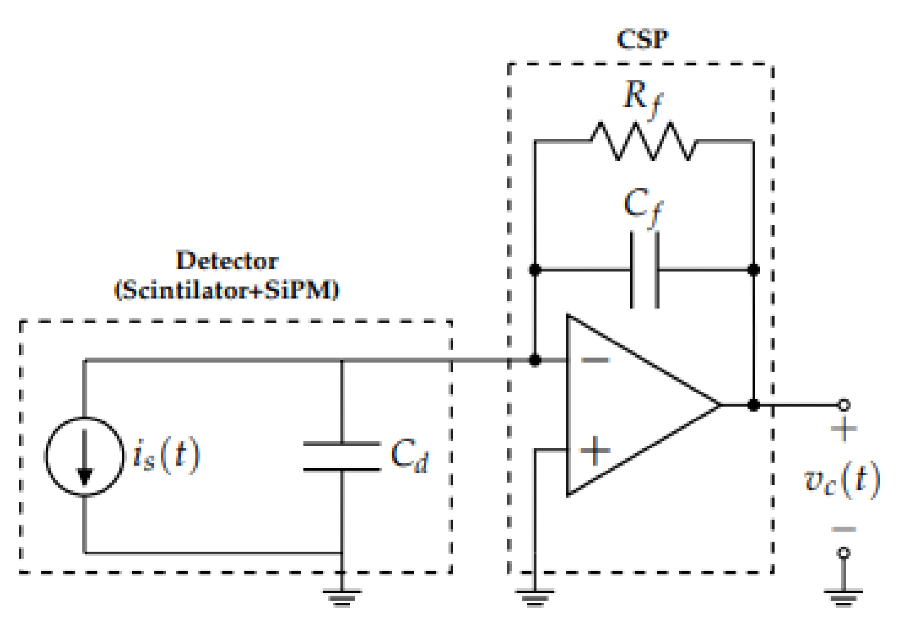 where is the SiPM terminal capacitance, is the integral capacitance, is the discharge resistance, which defines the accumulation time constant as .
Figure 4.
Charge Sensitive Preamplifier Circuit coupled to SiPM.
c. Pulse Shaper Circuit
Next, the amplified signal passes through a PSC. Regardless of the implementation, noise treatment through PSCs is a well-established topic, extensively addressed in the literature [1,6,10,40,41]. For instance, optimal pulse shaping in semiconductor detectors under various noise conditions has been widely explored, demonstrating robust methodologies in this field.
A reference study highlights the importance of understanding the purpose of pulse shaping in relation to specific measurement objectives [1]. In this context, the pulse shape refers to the mathematical function describing the waveform of the pulse, while the term "pulse" denotes the individual instance generated by the shaping system.
The semi-Gaussian shaper is a widely used design with many advantages, including simplicity in construction. It is typically implemented using CR-nRC circuits, where n commonly ranges from 1 to 4 [5,10,42,43]. However, some studies have extended this configuration to higher orders [7,11]. Active PSCs are also frequently employed, with configurations such as Sallen-Key filters providing enhanced flexibility and performance. Beyond analog implementations, digital pulse shaping circuits have garnered significant attention for their adaptability and precision, making them an attractive alternative in modern detection systems [5,6,7,10,43,44,45,46].
In this work, the PSC is modeled as a CR-4RC filter. The initial CR stage acts as a high-pass filter, removing low-frequency components and improving the temporal response by enabling faster signal transitions. The subsequent RC stages form a low-pass filter, attenuating high-frequency noise and smoothing rapid transients. The CR-4RC configuration was chosen to ensure that the pulse width is adequate for the sampling rate, as illustrated in Figure 5.
In addition to the number of integrator stages, selecting an appropriate time constant () is crucial for the proper operation of the PSC. The transfer function of the proposed circuit is presented in the following equation:
2.1.2.4. d. Noise Modeling
Noise analysis is crucial for understanding the performance of electronic circuits and sensors. In this analysis, we focus on the circuit assembled in the previous session, which includes the electronic equivalent of the detector, the CSP, and the PSC. While the physical response of the detector and SiPM is primarily measured in terms of deposited charge, electronic circuits typically use voltage and current as key quantities. Therefore, we will examine the noise contributions from the perspective of these electrical quantities and assess their impact on the impulse response of the system.
The primary type of noise to consider in this case is the thermal noise, which arises due to the random thermal agitation of charge carriers in conductors, resistors and semiconductor materials. This kind of noise is characterized by a broadband spectrum () with zero mean and a flat power spectrum density given by the following expression [38]:
where is the Boltzmann constant, T is the absolute temperature and R the resistante of the material or component. For this expression, we can consider this noise as ideal white noise, assuming that the bandwidth is sufficiently wide to encompass the noise contribution across all the relevant frequencies of our circuit. The noise power then is expressed as .
In this case, the noise originates from the internal resistances of the circuit, including those arising from the coupling between the detector and the CSP, as well as between the CSP and the PSC. These resistances encompass the sensor electrode resistance, the wiring or PCB traces, and the parasitic resistances in the amplifier transistors.
The noise power associated with these factors is represented by and , which correspond to the noise at the input of the preamplifier and shaper, respectively.
To evaluate the impact of the preamplifier noise on pulse compensation algorithms, we must pass it through the system and analyse the resulting frequency response. This requires considering the filtering effects of both the preamplifier (CSP) and the shaper (PSC) stages. The CSP exhibits a broad frequency spectrum with a low-pass characteristic, while the CR-4RC PSC acts as a band-pass filter.
At lower frequencies, the CSP shows a flat response up to its cutoff frequency, beyond which the response rolls off, attenuating higher-frequency noise components. The shaper, due to its band-pass characteristics, further shapes the system’s frequency response, suppressing both low and high frequencies while allowing a specific range of intermediate frequencies to pass.
As shown in the normalized magnitude plot (with a gain of 1 in the passband) in Figure 6, the shaper’s passband is largely contained within the preamplifier’s frequency response. Therefore, we can approximate the noise at the output of the preamplifier as white noise, with a standard deviation determined by the combined effect of the preamplifier input noise contributions.
The output noise power spectrum density at the output of the shaper can then be modeled as
In addition to the previously discussed noise sources, 1/f flicker noise (low-frequency noise) can play a significant role, especially in high-precision amplifiers commonly used in nuclear instrumentation circuits. This type of noise becomes more prominent at lower frequencies and can degrade system performance, particularly in applications requiring the detection of weak signals.
Current noise, which arises from fluctuations in current across various components and parasitic resistances, is another important factor. For example, variability in the avalanche currents of the SiPM’s photodetector pixels can introduce additional disturbances, further affecting the signal quality and measurement accuracy.
Although 1/f flicker noise and current noise are important, particularly in nuclear instrumentation circuits, they were not included in the current analysis. This choice was made to prioritize the primary noise sources that most significantly affect the system’s performance within the scope of this study.
2.2. Digital Processing
The events measured by the detector, after analog processing in the readout chain, are digitized with a sampling period , enabling the implementation of digital signal processing techniques. One such technique is the proposed deconvolution of the waveform using the unfolding method for modal components [13,47]. This approach optimizes the pulse shape and mitigates pileup effects, particularly in high-rate detection systems. The method focuses on converting the dominant exponential components of the waveform into impulses or, when this is not feasible, into step functions. This transformation preserves the amplitude of the original waveform while reducing the pulse width, thereby enhancing temporal resolution.
2.2.1. Unfolding Algorithm
The first step is to apply the unfolding algorithm to exponential components of the waveform. By deconvolving the exponential decay, the resulting signal is converted into a digital impulse, as proposed by Jordanov [14], and applied by Zeng [15], if all dominant component was removed, maintaining the original amplitude but with a reduced temporal width. This process significantly mitigates the pileup effects in high-rate environments.
Mathematically, this is achieved by considering that a discrete exponential signal, with a sampling period and a decay rate , can be represented in the recursive form:
where n is the sample number that is renationalized with the time and the parameter .
By subtracting the estimated sample from the actual sample, as shown in the equation, all terms for are canceled, while for the sample at , the resulting value is . This effectively recovers the unit impulse function [48].
where represents the input signal and the output signal with component remotion.
2.2.2. Pole Zero Cancellation
In the presence of a zero in the circuit’s dynamic response, the unfolding method becomes ineffective at removing one of the PSC poles due to the system being non-minimum phase. Consequently, an undershoot appears in the poles influenced by the zero, indicating the effect of a zero near the pole.
The distortion is introduced by the CR high-pass filter stage [47] when the parallel resistor is omitted. During a detector event, this causes a shift in the signal’s average level. Due to the capacitive coupling in the CR stage, which discharges slowly, this shift results in a displacement of the signal baseline, manifested as a negative component in the output. This negative component compensates for the increase in the signal’s average level caused by the event. When the detector’s signal undergoes a sudden change, such as during an event, the capacitors in the coupling network attempt to preserve the original voltage difference by generating a reverse polarity signal.
As the event rate increases, the cumulative effect of these shifts becomes more pronounced, resulting in a growing (falling) average signal level. This leads to an increase (decrease) in the baseline shift, which can have a significant impact on both the detection accuracy and the estimation of subsequent signal amplitudes. If left uncorrected, this distortion can lead to erroneous signal measurements, especially when the event rate is high.
Applying the unfolding method to these poles results in a train of unit impulses with oscillatory responses, specifically two impulses of opposite polarities. This behavior arises from the incomplete causality of the filter and follows the unitary impulse response as presented in Figure 8.
To mitigate this issue, the proposed solution integrates the response pulse of the unfolding algorithm using an accumulator. This results in a step-like function in the system’s output [16], with an amplitude gain of , which is lower than the original baseline shift, as presented in Figure 9. The compensation is achieved by applying the recursive formula:
here, represents the input signal (with distortion), is the output signal after compensation, and is a constant that depends on the exponential decay .
It is important to note that the baseline shift component is typically negative, which represents the ideal case to minimize confusion between the signal and the baseline. When this is not the case, modifications should be made to achieve this ideal condition.
Another procedure is necessary to compensate for the accumulation of step effects. A constant removal of the step influence is proposed in the implementation, as will be discussed in Section 2.3.2.
2.3. Hardware Implementation
The digital filter requires a hardware fast enough to process the data at the determined frequency rate. The Field Programmable Gate Array (FPGA) was chosen because it has the possibility to run the filtering process in real-time, with high frequencies, and it is largely used at online signal processing enviroments.
Most of FPGA chips works with fixed point, which means that the hardware does not do floating points operations natively. Two strategies can be traced to avoid this issue: first one is the floating point operations via emulation; the second is using quantization of the float point numbers. Both has their own pro and cons, for example, the first tends to use the more logic elements but it the operations are more precise, while the second approach normally uses less resource but it can insert approximation errors.
The development of the filtering and amplitude estimation for a real-time processing is described below and it was used the quantization technique.
2.3.1. PZC Implementation
The PZC for the hardware processing is done using the Equations 10 and 11. The two following equations are equivalent to the Equation 9, but here, for hardware implementation, the output signal is not normalized [47].
where v is the input signal of the PZC, M is the factor defined by . is the clock period of the system and is the time constant of the exponential decay. The factor M usually is a fixed number much greater than 10, which avoid the quantization of this number. The a factor and the M factor relation is , and the output signal has the original input amplitude multiplied by .
The Equation 10 describes an accumulator that is incrementing its value with the actual input reading. At FPGA, this is a register receiving, at each clock border, the adding result of its own value with the actual input signal. This work proposes to include a subtracting signal to the accumulator, here knows as Accumulator Correction (AC), to prevent some diverging results after long processing time. This step are detailed in the next subsection.
The PZC signal is the product between the M factor and the previous accumulator. This operation can be done with a continuos assignment approach, since the input data and the register are synchronized with the clock system. This M factor can be expressed as a parameter inside the block and is different for every pulse shape application that wishes to filter.
It is important to remember that the input data of PZC should be quantized if the fractional part influences at the result. The input signal bit size has to be defined correctly, as well as the register and output signal numbers of bits.
The Figure 10 is a block diagram that describes the PZC operations at the FPGA.
2.3.2. Accumulator Correction (AC)
The unfolding filter, when applied to an exponential undershooting component, produces a bipolar response that compromises the filtering process. This issue is addressed by combining the unfolding filter with an accumulator, which defines the PZC algorithm. The result is a step response with an amplitude lower than the original exponential component of the undershooting. The proposed approach prevents baseline divergence and ensures that residual processed information is effectively removed.
The chosen strategy involves analyzing a defined number of PZC output samples, calculating the mean of the negative values within this window, and subtracting it from the PZC accumulator. This compensation is applied at specific intervals, corresponding to the defined window size. Once the subtraction process is completed, the next correction is only performed after processing the next set of new samples. In other words, the compensation is not applied at every clock cycle. The process is detailed in Equation 12.
where r is the output signal of the PZC, p is the PZC accumulator and W is the window size for analysis.
For the FPGA implementation, three additional registers are utilized. The first register counts the total number of processed samples, the second counts the number of negative values within the window, and the third stores the sum of these negative values. The first counter increments at every clock cycle. Meanwhile, the logic checks whether the PZC output is negative. If the condition is met, the second counter is incremented, and the sample value is added to the third register.
When the first counter reaches the defined window size, the PZC accumulator is adjusted by subtracting the ratio of the sum of negative values (stored in the third register) to the second counter. After this operation, all counters and the register holding the sum of negative values are reset, allowing the process to restart for the next set of samples.
2.3.3. Unfolding Filter
The unfolding filter represents the next step in the implementation. It uses the PZC output to identify the impulse response that reflects the particle’s energy, focusing solely on canceling stable poles. This approach effectively isolates zeros in the transfer function, allowing the filter to operate as a finite impulse response (FIR) difference filter [49].
The FIR filter performs the deconvolution process and it is a simple method to be implemented in an online environment, specially at FPGA. First, the weights are defined according the filter order and the values are predefined to match with the application. Again, as the filter weights might be a float point number, its common to quantify theses values. This paper uses the quantization that less affect the final results, reaching a similar results when compared to the exactly weights float point values.
After defining the weights, the input samples are delayed following the filter order to match the related weight of that sample. The final result of the FIR filter is given by the sum of multiplication products between the delayed samples and the corresponding weight.
In the proposed application, there is two consecutive FIR filters, one for each signal component filtering. The structure of both are the same, with order two, same quantization but their weights are different. With the FIR filter processes done, the output expected is the impulsive energy that wants to be reconstructed. The Figure 13 represents the block diagram of the FIR filter implementation.
3. Results
To evaluate the performance of the proposed signal processing approach, the system parameters were carefully defined, and simulations were conducted under realistic operating conditions. The system’s time constants were used to calculate the filter coefficients, aligning the processing stages with the pulse dynamics of the readout chain. The dominant poles of the system, responsible for shaping the waveform, were addressed using the unfolding algorithm. Meanwhile, poles near marginal stability were handled with the PZC approach to ensure proper baseline correction.
The results include the waveforms generated by MATLAB simulations at different stages of the readout chain, , along with metrics such as baseline shift () and pileup level (), both before and after applying the proposed algorithms. The performance of the algorithms is verified through FPGA implementations to validate the effectiveness of the proposed methods.
3.1. Readout Waveform
The desing performance of the CSP and the PSC is directly influenced by their design parameters, particularly the time constants chosen for each stage. These time constants are critical for balancing pulse width, noise reduction, and temporal resolution, ensuring that the output signal meets the requirements of high-rate detection systems.
The response obtained from the CSP combines the contributions from the scintillator, SiPM, and preamplifier. The time constants chosen for the scintillator and SiPM were based on values from previous studies [3,34], where the rise time is , and the decay time is and the SiPM capacitance was define as . The time constant for the CSP was set to [5,44].
Similarly, the time constant for the PSC was also defined, being the same for the differentiator stage and the integrator stages (), with a value .
It is worth noting that the chosen digitization period was , which was one of the primary factors influencing the definition of the time constants in the shaper circuit, ensuring proper digitization.
Figure 14 illustrates the impulse response of the CSP and PSC stages separately, highlighting the contribution of each component according to the selected time constants. In the bottom plot, the broadening effect induced by the semi-Gaussian shaper is evident. This broadening results from the low-pass filtering characteristics of the shaper, which attenuates high-frequency noise while widening the pulse. This pulse widening enhances the signal-to-noise ratio (SNR) and ensures that the full charge is collected and accurately measured.
Finally, Figure 15 presents the effect of the combined CSP and PSC system on the overall pulse. The plot clearly reveals a significant long-tail component in the pulse’s response, with a decay time that is approximately three orders of magnitude longer than both the rise and decay times of the initial signal.
The poles and zeros of the acquisition system, along with their associated time constants, are shown in Figure 16. The inset highlights the dominant poles and a pole nearing instability.
The proposed approach involves canceling the two dominant poles using the unfolding method and addressing the marginally stable pole with the PZC algorithm.
3.2. Evaluation Metrics
The pileup level quantification is an important metric to evaluate the performance of detectors. Pileup is a random effect where events follow a Poisson time distribution, influenced by the event rate () and the pulse width (). According to Campbell’s theorem [50], the probability of N pulses occurring within a time interval equal to the pulse width is given by the equation:
However, to define a pileup level () metric that is independent of the number of overlapping events, the complement of the probabilities of exactly one event and zero events occurring within the interval is calculated. This approach quantifies the probability of pileup involving two or more events within the same interval. Consequently, the is given by:
Similarly, it is necessary to quantify the baseline shift of the pulse. In this case, the proposed approach is to calculate the average of the negative signal, as given by the equation, since in the context of energy detection from particle interactions, only non-negative values are expected. Therefore, any baseline shift or other alterations to the signal result in negative values [51].
where, is a representation of is the time constant from the negative component that generates the undershooting.
3.3. Algorithm Verification in Hardware Implementation
The verification of the algorithms was carried out on their hardware implementation on an FPGA. The primary focus of this step is to validate the effectiveness of the unfolding and PZC algorithms under streaming processing conditions.
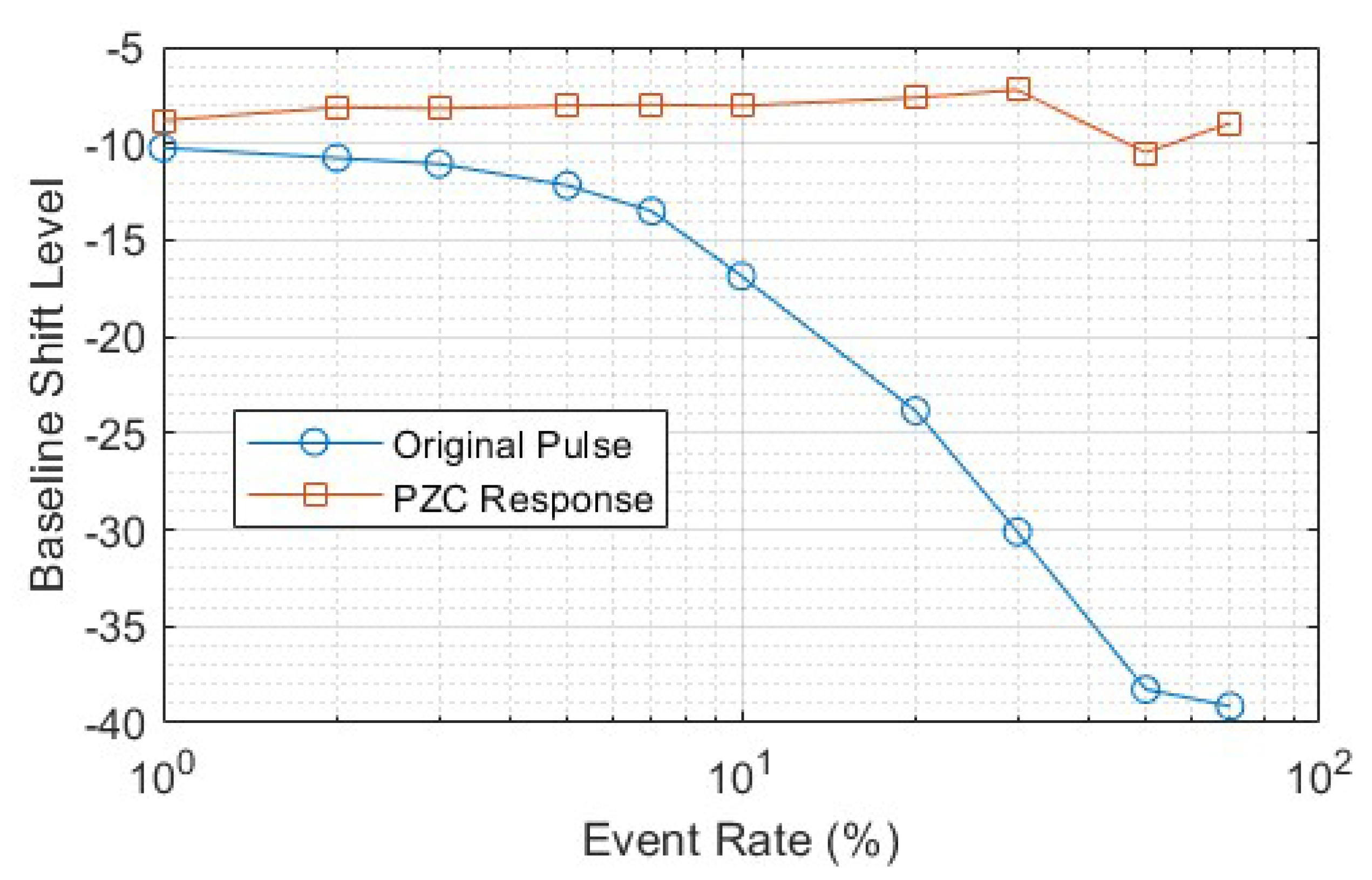
The baseline shift, measured by the BL, introduced by the capacitive coupling in the readout chain was initially quantified for the simulated signal. After applying the PZC algorithm, the baseline was effectively restored, as indicated by a significant reduction in the BL metric, approaching the ideal baseline level, when compared to the BL befor the PZC, as presented in Figure 17.
The unfolding algorithm’s performance is assessed by comparing the PL before and after processing, demonstrating its ability to mitigate pulse overlap.
Figure 18.
Pileup level as a function of event rate.
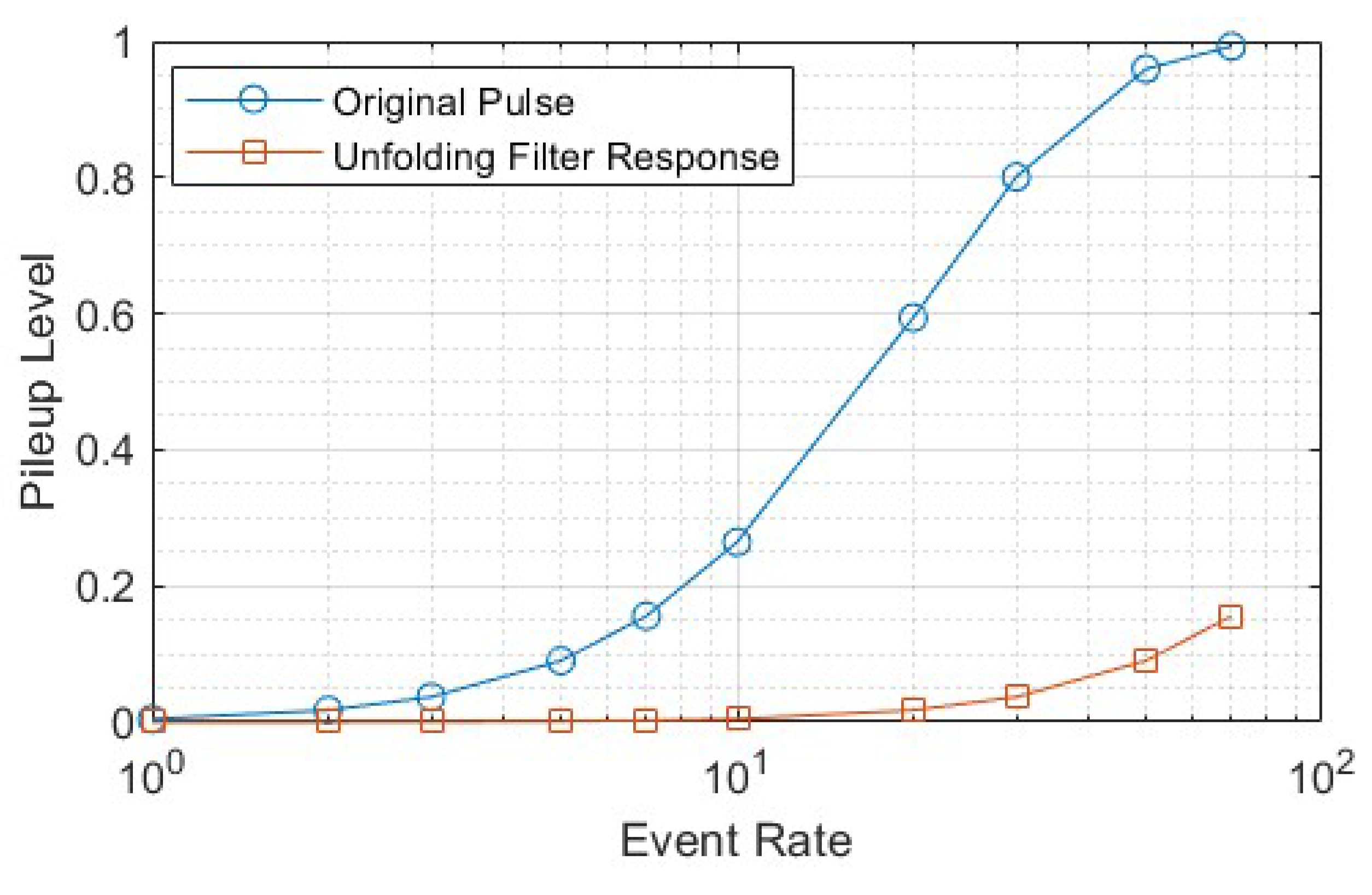
Pileup and baseline shift become more pronounced at higher event rates. Nevertheless, the unfolding algorithm effectively mitigated pileup, while the PZC algorithm efficiently compensated for baseline shift.
4. Discussion
The implementation of the PZC algorithm significantly reduced baseline shift, lowering it from -40 ADC units at high event rate levels to approximately -10 ADC units. This residual shift closely approaches the baseline observed lower than 10% event rate and remains only slightly above the noise standard deviation of 5 ADC units. This demonstrates the algorithm’s effectiveness in mitigating baseline shift across the full range of event rates (1% to 70% event rate). Moreover, the PZC algorithm enhanced the system’s performance by improving the signal-to-noise ratio, thereby increasing detection accuracy and refining charge collection resolution.
Furthermore, the application of the unfolding filter effectively addressed pileup artifacts. For event rates up to 10–20%, the filter reduced the pileup probability to nearly 0%, compared to an unprocessed pulse that exhibited a pileup probability of approximately 30%. Even at higher event rates, up to 30% event rate, while the pileup probability for unfiltered pulses approached 100%, the unfolding filter maintained the pileup probability below 20%. This performance underscores the robustness of the unfolding filter in preserving signal integrity across a broad spectrum of operational conditions.
Author Contributions
Conceptualization, T.M.Q., T.C.A.P., P.H.B.L. and L.M.A.F.; methodology, T.M.Q., T.C.A.P. and P.H.B.L.; software, T.M.Q., T.C.A.P and G.I.G.; validation, T.M.Q., T.C.A.P. and G.I.G; formal analysis, T.M.Q., T.C.A.P. and L.M.A.F.; data curation, B.S.P. and G.I.G.; writing—original draft preparation, T.M.Q and T.C.A.P.; writing—review and editing, T.M.Q., T.C.A.P., L.M.A.F. and B.S.P.; visualization, X.X.; supervision, L.M.A.F. and B.S.P.; All authors have read and agreed to the published version of the manuscript.
Funding
This research was funded by Fundação Carlos Chagas Filho de Amparo à Pesquisa do Estado do Rio de Janeiro (FAPERJ) grant number E-26/201.304/2022.
Data Availability Statement
The original data presented in the study are openly available at https://cernbox.cern.ch/s/pcP0kY5VxB4gsZ5.
Acknowledgments
The authors are thankful to CAPES, CNPq, FAPERJ, FAPEMIG and RENAFAE for the support. This study was financed in part by the Coordenação de Aperfeiçoamento de Pessoal de Nível Superior – Brasil (CAPES) – Finance Code 001.
Conflicts of Interest
The authors declare no conflicts of interest.
References
- Spieler, H. Pulse processing and analysis. IEEE Nuclear Science Symposium Short Course; IEEE: San Francisco, 2002; pp. 52–90.
- Conti, M.; Bendriem, B. The new opportunities for high time resolution clinical TOF PET. Clinical and Translational Imaging 2019, 7, 139–147. [CrossRef]
- Park, H.; Yi, M.; Lee, J.S. Silicon photomultiplier signal readout and multiplexing techniques for positron emission tomography: a review. Biomedical engineering letters 2022, 12, 263–283. [CrossRef]
- Spieler, H. Semiconductor detector systems; Vol. 12, Oxford university press, 2005.
- Aimaier, N.; Sidek, R.M.; Hamidon, M.N.; Sulaiman, N. Transistor sizing methodology for low noise charge sensitive amplifier with input transistor working in moderate inversion. 2014 IEEE International Conference on Semiconductor Electronics (ICSE2014), 2014, pp. 189–192. [CrossRef]
- Noulis, T.; Fikos, G.; Sarrabayrouse, G.; Siskos, S. Noise analysis of radiation detector charge sensitive amplifier architectures 2008.
- Gallin-Martel, L.; Pouxe, J.; Rossetto, O.; Yamouni, A. A 16 channel analog integrated circuit for PMT pulses processing. IEEE Nuclear Science Symposium; IEEE: San Diego, 2001; pp. 742–745.
- Knoll, G.F. Radiation detection and measurement; John Wiley & Sons, 2010.
- Beckhoff, B.; Kanngießer, B.; Langhoff, N.; Wedell, R.; Wolff, H. Handbook of practical X-ray fluorescence analysis; Springer Science & Business Media: Berlin, 2007; pp. 251–255, 260–261.
- Nakhostin, M. Recursive algorithms for real-time digital CR-RCn pulse shaping. IEEE Transactions on Nuclear Science 2011, 58, 2378–2381. [CrossRef]
- Sosa, C.; Flaska, M.; Pozzi, S. Comparison of analog and digital pulse-shape-discrimination systems. Nuc. Instrum. Methods in Phys. Res. A 2016, 826, 72–79. [CrossRef]
- Di Fulvio, A.; Shin, T.; Hamel, M.; Pozzi, S. Digital pulse processing for NaI (Tl) detectors. Nuc. Instrum. Methods in Phys. Res. A 2016, 806, 169–174. [CrossRef]
- Jordanov, V.T. Deconvolution of pulses from a detector-amplifier configuration. Nuc. Instrum. Methods in Phys. Res. A 1994, 351, 592–594. [CrossRef]
- Jordanov, V.T. Unfolding-synthesis technique for digital pulse processing. Part 1: Unfolding. Nuclear Instruments and Methods in Physics Research Section A: Accelerators, Spectrometers, Detectors and Associated Equipment 2016, 805, 63–71. [CrossRef]
- Zeng, G.Q.; Yang, J.; Yu, M.F.; Zhang, K.Q.; Ge, Q.; Ge, L.Q. Digital pulse deconvolution method for current tails of NaI (Tl) detectors. Chin. Phys. C 2017, 41, 016102. [CrossRef]
- Födisch, P.; Wohsmann, J.; Lange, B.; Schönherr, J.; Enghardt, W.; Kaever, P. Digital high-pass filter deconvolution by means of an infinite impulse response filter. Nuc. Instrum. Methods in Phys. Res. A 2016, 830, 484–496. [CrossRef]
- Stezelberger, T.; Zimmermann, S. One and Two Poles Compensation of Charge Sensitive Amplifiers with Resistive Feedback to Improve the Energy Resolution in GRETA. IEEE Transactions on Nuclear Science 2023. [CrossRef]
- Jordanov, V.T. Exponential signal synthesis in digital pulse processing. Nuclear Instruments and Methods in Physics Research Section A: Accelerators, Spectrometers, Detectors and Associated Equipment 2012, 670, 18–24. [CrossRef]
- da Fonseca Pinto, J.V.; Marin, J.L.; Freund, W.; Milan, G.G.; de Araújo, M.V.; Gonçalves, G. lorenzetti-hep/lorenzetti: 2.0.0, 2022. [CrossRef]
- Collaboration*, I. Evidence for high-energy extraterrestrial neutrinos at the IceCube detector. Science 2013, 342, 1242856. [CrossRef]
- Campana, S.; Wenaus, T. The ATLAS computing challenge for HL-LHC. Technical report, CERN, 2016.
- Moon, C.S. A level-1 pixel based track trigger for the CMS HL-LHC upgrade. Technical report, CERN, 2016.
- Benedikt, M.; Blondel, A.; Janot, P.; Mangano, M.; Zimmermann, F. Future circular colliders succeeding the LHC. Nature Physics 2020, 16, 402–407. [CrossRef]
- Klochkov, V.; Collaboration, C.; others. The compressed baryonic matter experiment at fair. Nuclear Physics A 2021, 1005, 121945. [CrossRef]
- Smy, M.B. Hyper-Kamiokande. Physical Sciences Forum. MDPI, 2023, Vol. 8, p. 41. [CrossRef]
- Wigmans, R. Calorimetry: Energy measurement in particle physics; Oxford University Press, 2000.
- Bierlich, C.; Chakraborty, S.; Desai, N.; Gellersen, L.; Helenius, I.; Ilten, P.; Lönnblad, L.; Mrenna, S.; Prestel, S.; Preuss, C.T.; Sjöstrand, T.; Skands, P.; Utheim, M.; Verheyen, R. A comprehensive guide to the physics and usage of PYTHIA 8.3. SciPost Phys. Codebases 2022, p. 8. [CrossRef]
- Agostinelli, S.; Allison, J.; Amako, K.; Apostolakis, J.; Araujo, H.; Arce, P.; Asai, M.; Axen, D.; Banerjee, S.; Barrand, G.; Behner, F.; Bellagamba, L.; Boudreau, J.; Broglia, L.; Brunengo, A.; Burkhardt, H.; Chauvie, S.; Chuma, J.; Chytracek, R.; Cooperman, G.; Cosmo, G.; Degtyarenko, P.; Dell’Acqua, A.; Depaola, G.; Dietrich, D.; Enami, R.; Feliciello, A.; Ferguson, C.; Fesefeldt, H.; Folger, G.; Foppiano, F.; Forti, A.; Garelli, S.; Giani, S.; Giannitrapani, R.; Gibin, D.; Gómez Cadenas, J.; González, I.; Gracia Abril, G.; Greeniaus, G.; Greiner, W.; Grichine, V.; Grossheim, A.; Guatelli, S.; Gumplinger, P.; Hamatsu, R.; Hashimoto, K.; Hasui, H.; Heikkinen, A.; Howard, A.; Ivanchenko, V.; Johnson, A.; Jones, F.; Kallenbach, J.; Kanaya, N.; Kawabata, M.; Kawabata, Y.; Kawaguti, M.; Kelner, S.; Kent, P.; Kimura, A.; Kodama, T.; Kokoulin, R.; Kossov, M.; Kurashige, H.; Lamanna, E.; Lampén, T.; Lara, V.; Lefebure, V.; Lei, F.; Liendl, M.; Lockman, W.; Longo, F.; Magni, S.; Maire, M.; Medernach, E.; Minamimoto, K.; Mora de Freitas, P.; Morita, Y.; Murakami, K.; Nagamatu, M.; Nartallo, R.; Nieminen, P.; Nishimura, T.; Ohtsubo, K.; Okamura, M.; O’Neale, S.; Oohata, Y.; Paech, K.; Perl, J.; Pfeiffer, A.; Pia, M.; Ranjard, F.; Rybin, A.; Sadilov, S.; Di Salvo, E.; Santin, G.; Sasaki, T.; Savvas, N.; Sawada, Y.; Scherer, S.; Sei, S.; Sirotenko, V.; Smith, D.; Starkov, N.; Stoecker, H.; Sulkimo, J.; Takahata, M.; Tanaka, S.; Tcherniaev, E.; Safai Tehrani, E.; Tropeano, M.; Truscott, P.; Uno, H.; Urban, L.; Urban, P.; Verderi, M.; Walkden, A.; Wander, W.; Weber, H.; Wellisch, J.; Wenaus, T.; Williams, D.; Wright, D.; Yamada, T.; Yoshida, H.; Zschiesche, D. Geant4—a simulation toolkit. Nuclear Instruments and Methods in Physics Research Section A: Accelerators, Spectrometers, Detectors and Associated Equipment 2003, 506, 250–303. [CrossRef]
- Allison, J.; Amako, K.; Apostolakis, J.; Araujo, H.; Arce Dubois, P.; Asai, M.; Barrand, G.; Capra, R.; Chauvie, S.; Chytracek, R.; Cirrone, G.; Cooperman, G.; Cosmo, G.; Cuttone, G.; Daquino, G.; Donszelmann, M.; Dressel, M.; Folger, G.; Foppiano, F.; Generowicz, J.; Grichine, V.; Guatelli, S.; Gumplinger, P.; Heikkinen, A.; Hrivnacova, I.; Howard, A.; Incerti, S.; Ivanchenko, V.; Johnson, T.; Jones, F.; Koi, T.; Kokoulin, R.; Kossov, M.; Kurashige, H.; Lara, V.; Larsson, S.; Lei, F.; Link, O.; Longo, F.; Maire, M.; Mantero, A.; Mascialino, B.; McLaren, I.; Mendez Lorenzo, P.; Minamimoto, K.; Murakami, K.; Nieminen, P.; Pandola, L.; Parlati, S.; Peralta, L.; Perl, J.; Pfeiffer, A.; Pia, M.; Ribon, A.; Rodrigues, P.; Russo, G.; Sadilov, S.; Santin, G.; Sasaki, T.; Smith, D.; Starkov, N.; Tanaka, S.; Tcherniaev, E.; Tome, B.; Trindade, A.; Truscott, P.; Urban, L.; Verderi, M.; Walkden, A.; Wellisch, J.; Williams, D.; Wright, D.; Yoshida, H. Geant4 developments and applications. IEEE Transactions on Nuclear Science 2006, 53, 270–278. [CrossRef]
- Araújo, M.; Begalli, M.; Freund, W.; Gonçalves, G.; Khandoga, M.; Laforge, B.; Leopold, A.; Marin, J.; Peralva, B.M.; Pinto, J.; Santos, M.; Seixas, J.; Simas Filho, E.; Souza, E. Lorenzetti Showers - A general-purpose framework for supporting signal reconstruction and triggering with calorimeters. Computer Physics Communications 2023, 286, 108671. [CrossRef]
- Araújo, M.; Begalli, M.; Freund, W.; Gonçalves, G.; Khandoga, M.; Laforge, B.; Leopold, A.; Marin, J.; Peralva, B.M.; Pinto, J.; Santos, M.; Seixas, J.; Simas Filho, E.; Souza, E. Lorenzetti Showers - A general-purpose framework for supporting signal reconstruction and triggering with calorimeters. Computer Physics Communications 2023, 286, 108671. [CrossRef]
- Wright, A. The photomultiplier handbook; Oxford University Press: Oxford, 2017; p. 553.
- Li, Y.; Chen, L.; Gao, R.; Liu, B.; Zheng, W.; Zhu, Y.; Ruan, J.; Ouyang, X.; Xu, Q. Nanosecond and highly sensitive scintillator based on all-inorganic perovskite single crystals. ACS Applied Materials & Interfaces 2021, 14, 1489–1495. [CrossRef]
- Hu, C.; Zhang, L.; Zhu, R.Y. Fast and Radiation Hard Inorganic Scintillators for Future HEP Experiments. Journal of Physics: Conference Series. IOP Publishing, 2022, Vol. 2374, p. 012110. [CrossRef]
- Sánchez, D.; Gómez, S.; Fernández-Tenllado, J.M.; Ballabriga, R.; Campbell, M.; Gascón, D. Multimodal simulation of large area silicon photomultipliers for time resolution optimization. Nuclear Instruments and Methods in Physics Research Section A: Accelerators, Spectrometers, Detectors and Associated Equipment 2021, 1001, 165247. [CrossRef]
- Garutti, E.; Klanner, R.; Rolph, J.; Schwandt, J. Simulation of the response of SiPMs; Part I: Without saturation effects. Nuclear Instruments and Methods in Physics Research Section A: Accelerators, Spectrometers, Detectors and Associated Equipment 2021, 1019, 165853. [CrossRef]
- Bolic, M.; Drndarevic, V.; Gueaieb, W. Pileup correction algorithms for very-high-count-rate gamma-ray spectrometry with NaI (Tl) detectors. IEEE Transactions on Instrumentation and Measurement 2009, 59, 122–130. [CrossRef]
- Polushkin, V. Nuclear Electronics: Superconducting Detectors and Processing Techniques; John Wiley & Sons, 2004.
- Ching-Roa, V.D.; Olson, E.M.; Ibrahim, S.F.; Torres, R.; Giacomelli, M.G. Ultrahigh-speed point scanning two-photon microscopy using high dynamic range silicon photomultipliers. Scientific Reports 2021, 11, 5248. [CrossRef]
- Gatti, E.; Geraci, A.; Ripamonti, G. Optimum time-limited filters for input signals of arbitrary shape. Nuclear Instruments and Methods in Physics Research Section A: Accelerators, Spectrometers, Detectors and Associated Equipment 1997, 395, 226–230. [CrossRef]
- Zhang, Y.; Zhang, Q.; Zhang, Y.; Pei, J.; Huang, Y.; Yang, J. Fast split bregman based deconvolution algorithm for airborne radar imaging. Remote Sensing 2020, 12, 1747. [CrossRef]
- Grybos, P.; Maj, P.; Ramello, L.; Swientek, K. Measurements of matching and high count rate performance of multichannel ASIC for digital X-ray imaging systems. IEEE Transactions on Nuclear Science 2007, 54, 1207–1215. [CrossRef]
- Liu, K.; Zhou, R.; Zhang, W.; Tang, Z.; Yan, J.; Lv, M.; Li, X.; Lu, Y.; Zeng, X. Interference correction for laser-induced breakdown spectroscopy using a deconvolution algorithm. Journal of Analytical Atomic Spectrometry 2020, 35, 762–766. [CrossRef]
- Lin, M.C.; Syrzycki, M. Current source transistor optimization methodology for noise optimized charge sensitive amplifier with fast shaper. 2011 24th Canadian Conference on Electrical and Computer Engineering (CCECE). IEEE, 2011, pp. 000735–000738.
- Zhang, H.Q.; Qian, Y.c.; Chen, H.; Shi, H.t. Design and characterization of third-order Sallen–Key digital filter in nuclear signal processing. Applied Radiation and Isotopes 2022, 186, 110277. [CrossRef]
- Liu, G.; Lai, W.; Jiang, Y.; Shi, J. Design of Experimental Circuit Board of Spectrometer Amplifier in Nuclear Electronics. Journal of Physics: Conference Series. IOP Publishing, 2023, Vol. 2440, p. 012008. [CrossRef]
- Jordanov, V.T.; Knoll, G.F.; Huber, A.C.; Pantazis, J.A. Digital techniques for real-time pulse shaping in radiation measurements. Nuc. Instrum. Methods Phys. Res. A 1994, 353, 261–264. [CrossRef]
- Liu, Y.; Wang, M.; Wan, W.; Zhou, J.; Hong, X.; Liu, F.; Yu, J. Counting-loss correction method based on dual-exponential impulse shaping. Journal of Synchrotron Radiation 2020, 27, 1609–1613. [CrossRef]
- Meyer-Baese, U.; Meyer-Baese, U. Digital signal processing with field programmable gate arrays; Vol. 65, Springer, 2007.
- Du, Z.; Chen, X.; Zhang, H. Convolutional sparse learning for blind deconvolution and application on impulsive feature detection. IEEE Transactions on Instrumentation and Measurement 2018, 67, 338–349. [CrossRef]
- Khilkevitch, E.; Shevelev, A.; Chugunov, I.; Iliasova, M.; Doinikov, D.; Gin, D.; Naidenov, V.; Polunovsky, I. Advanced algorithms for signal processing scintillation gamma ray detectors at high counting rates. Nuclear Instruments and Methods in Physics Research Section A: Accelerators, Spectrometers, Detectors and Associated Equipment 2020, 977, 164309. [CrossRef]
Figure 1.
Block diagram of detector’s readout chain.
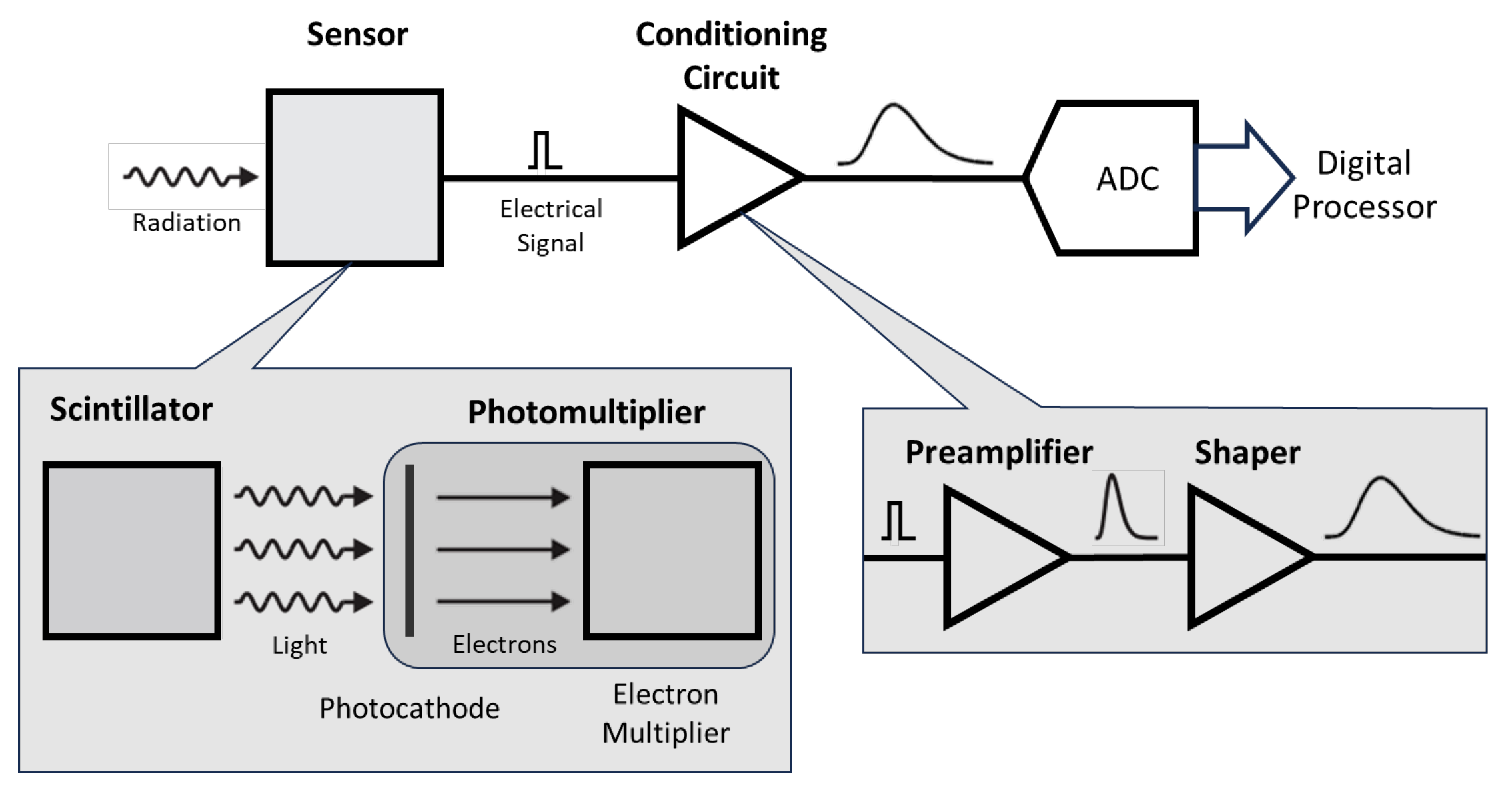
Figure 2.
Pileup effect.
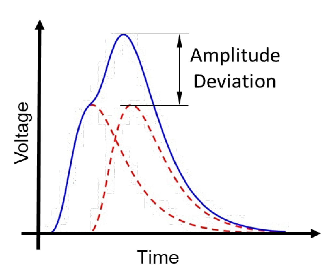
Figure 3.
Baseline Shift effect.
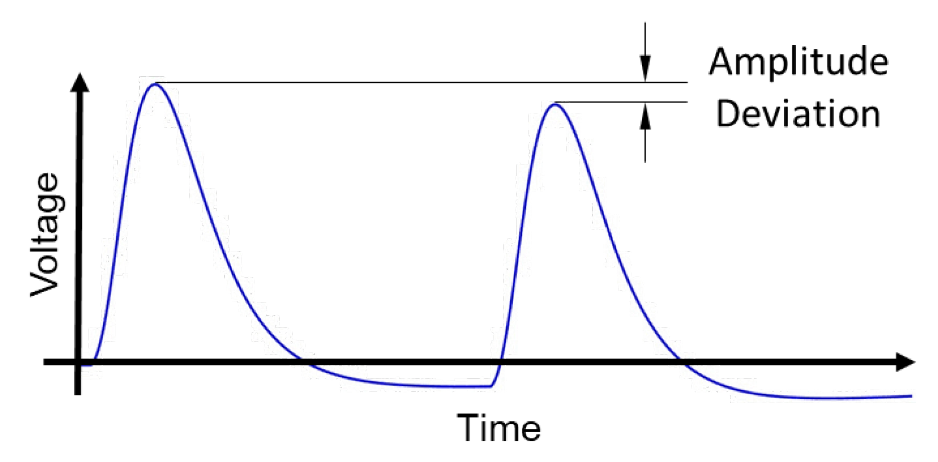
Figure 5.
Pulse Shaper circuit.
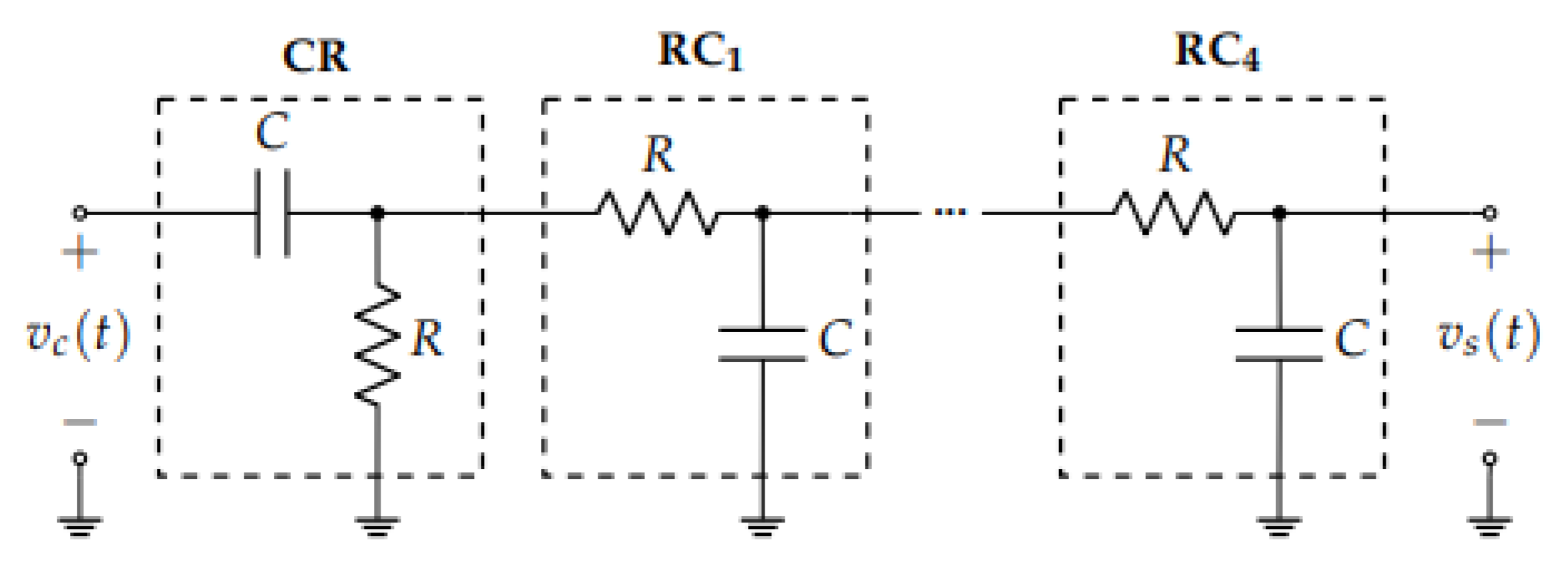
Figure 6.
Normalized Frequency Response of the CSP and Shaper circuits.
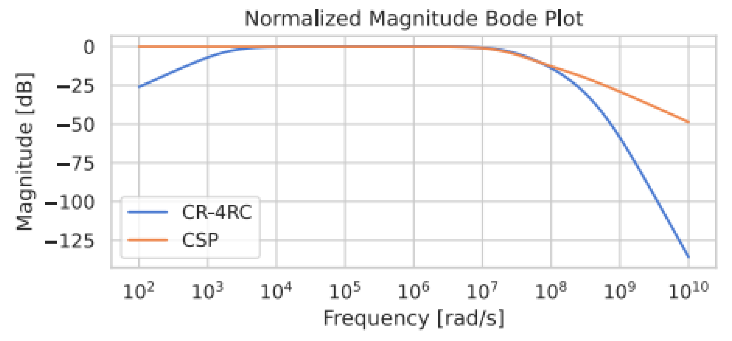
Figure 7.
Unfolding Algorithm.
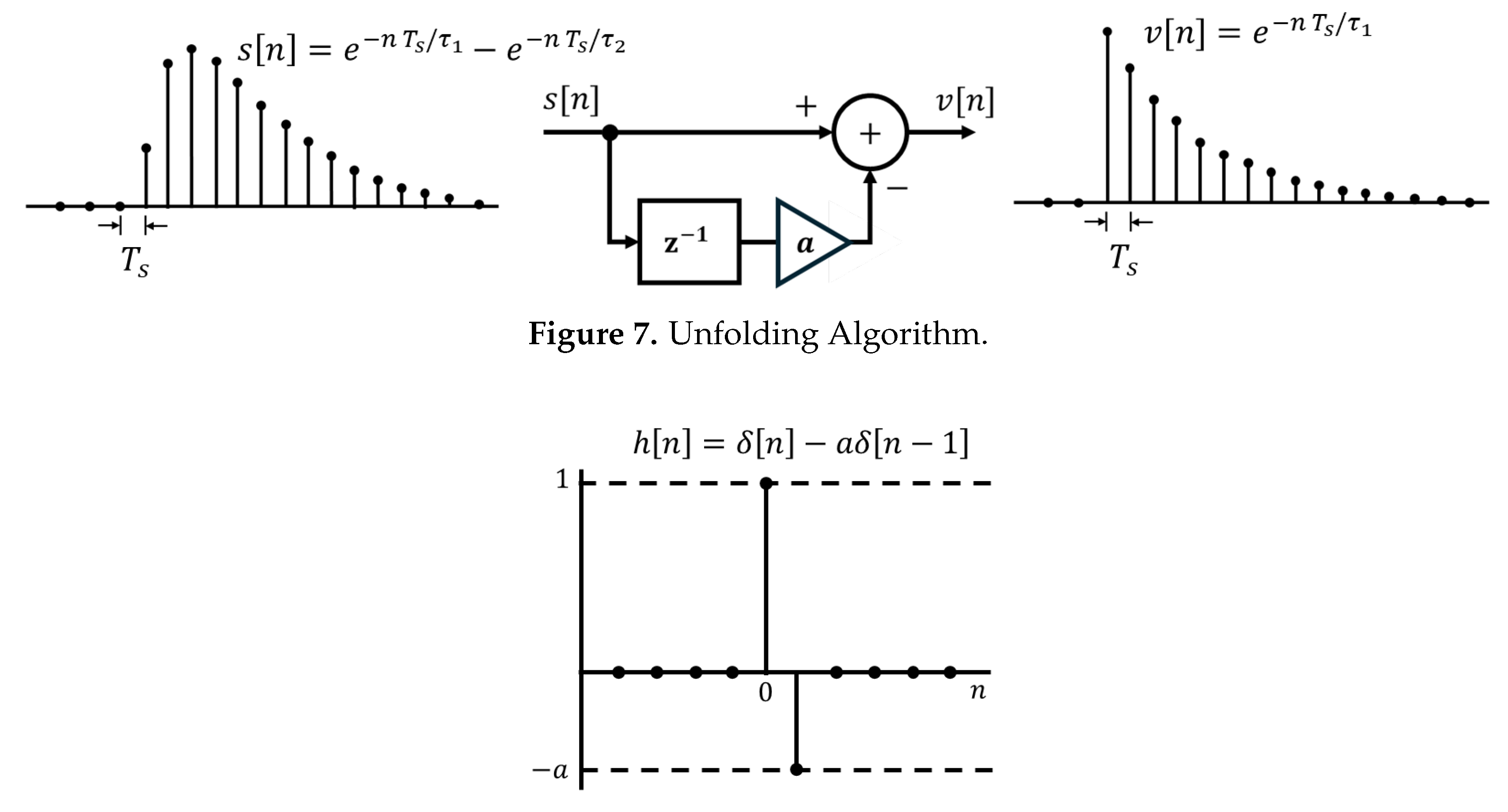
Figure 8.
Unfolding Impulse Response.
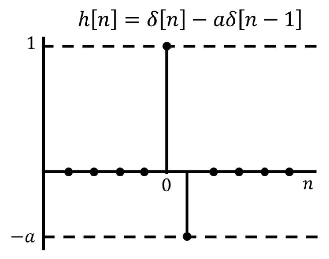
Figure 9.
Accumulated Unfolding Impulse Response.
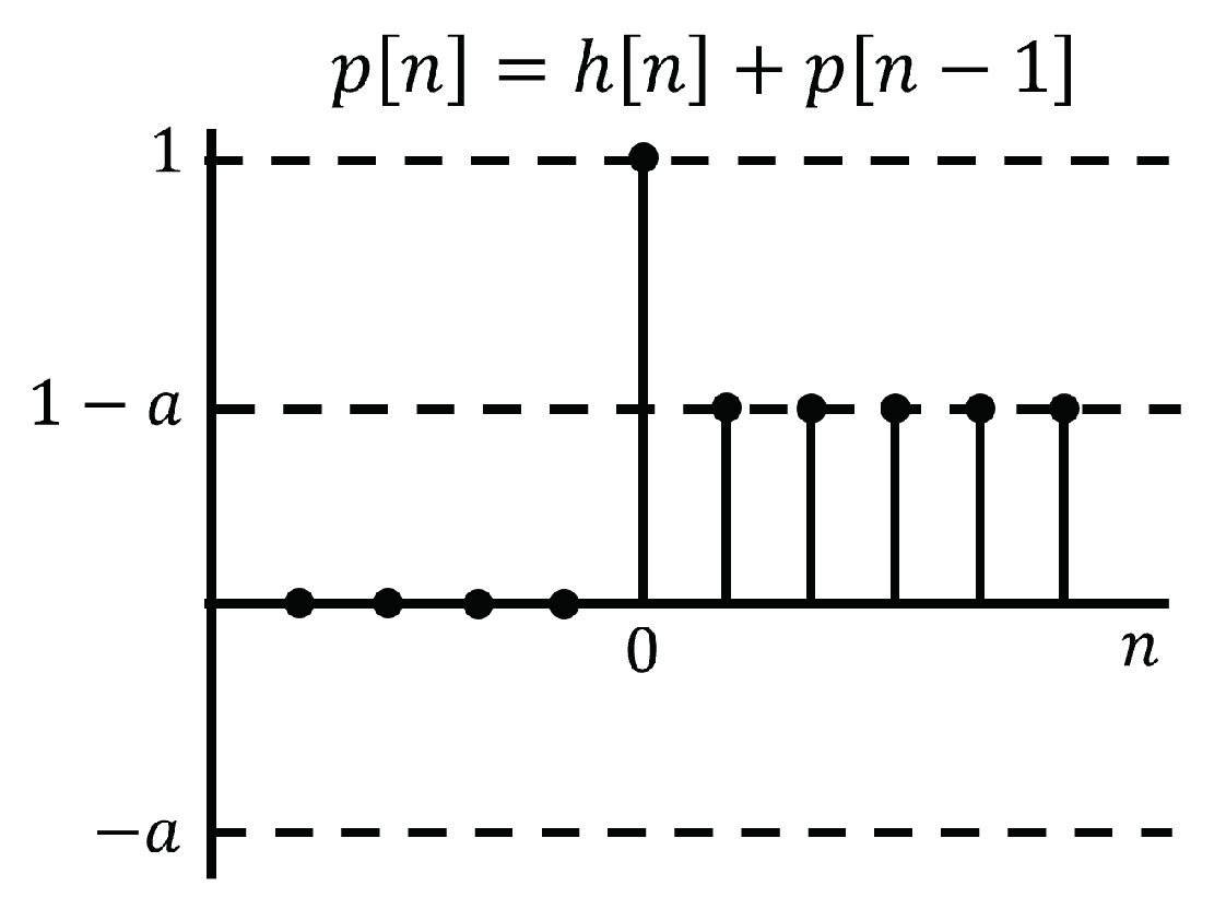
Figure 10.
Block Diagram of the PZC at FPGA.
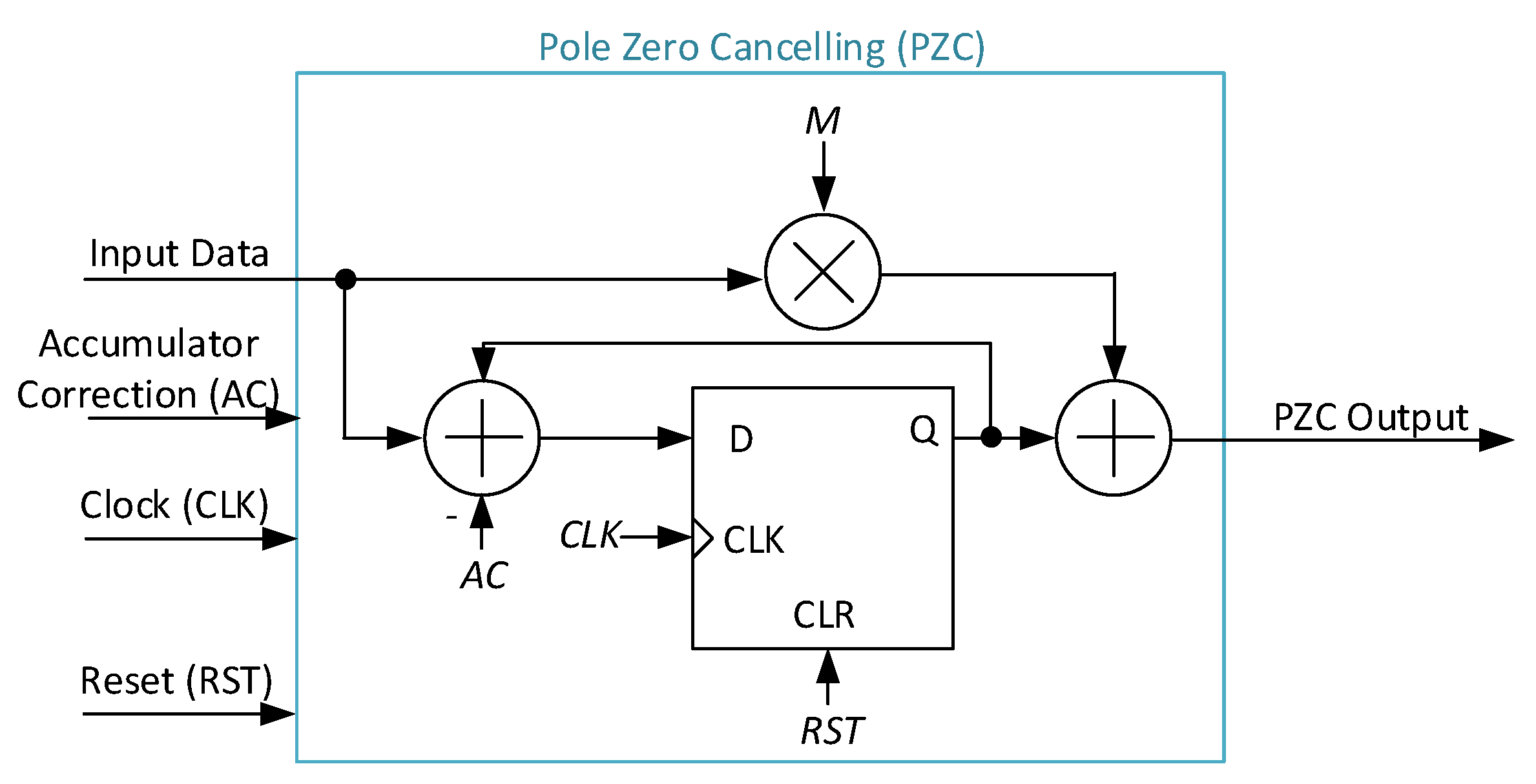
Figure 11.
Block Diagram of the AC at FPGA.
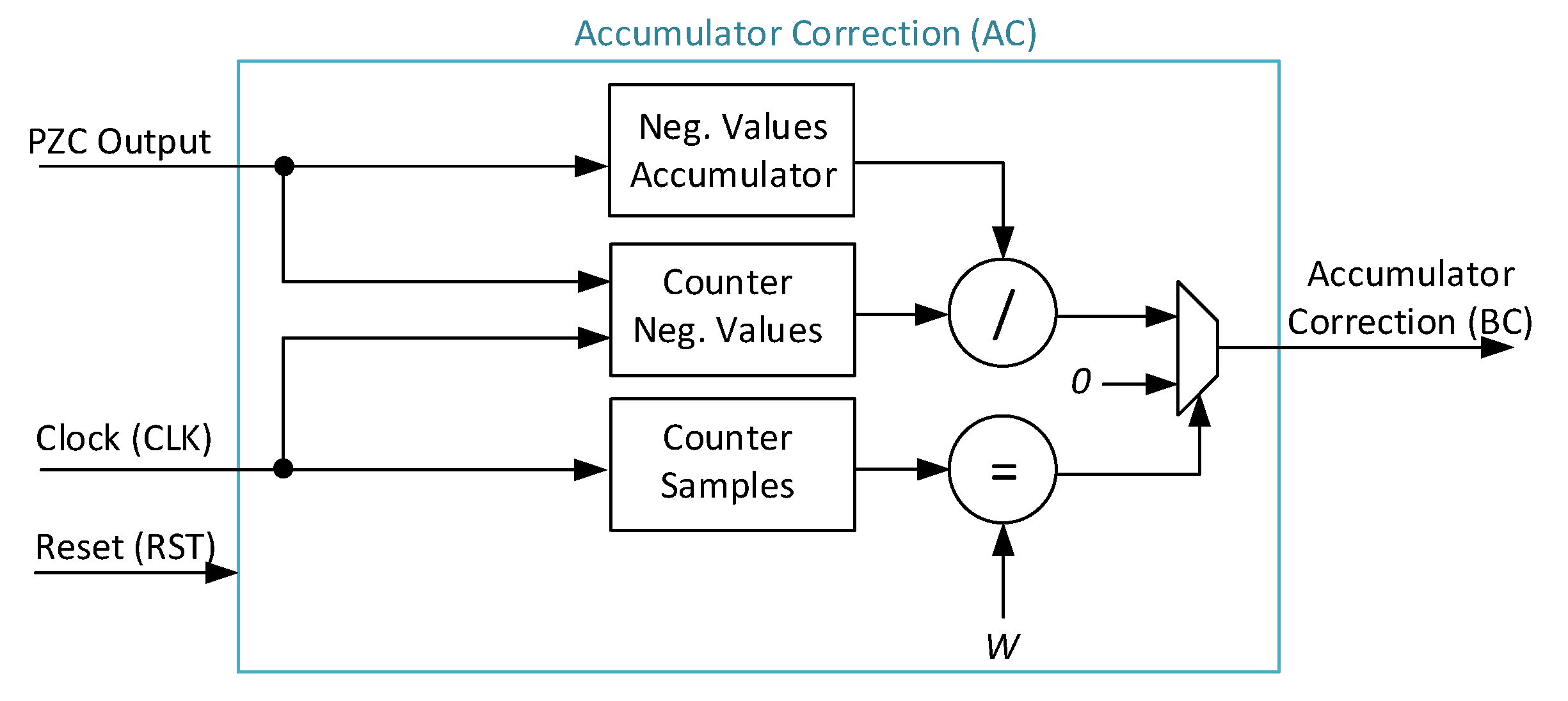
Figure 12.
Relation between AC and PZC at FPGA.
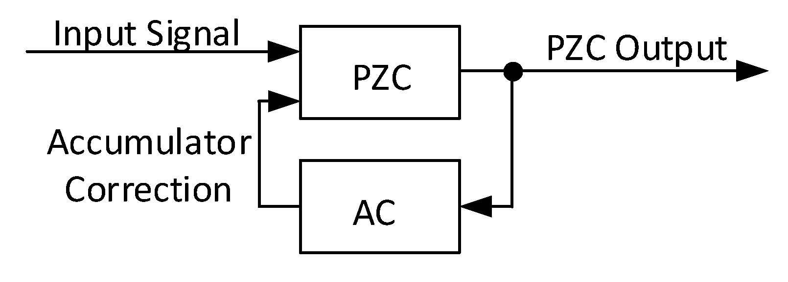
Figure 13.
Block Diagram of the FIR filter at FPGA.
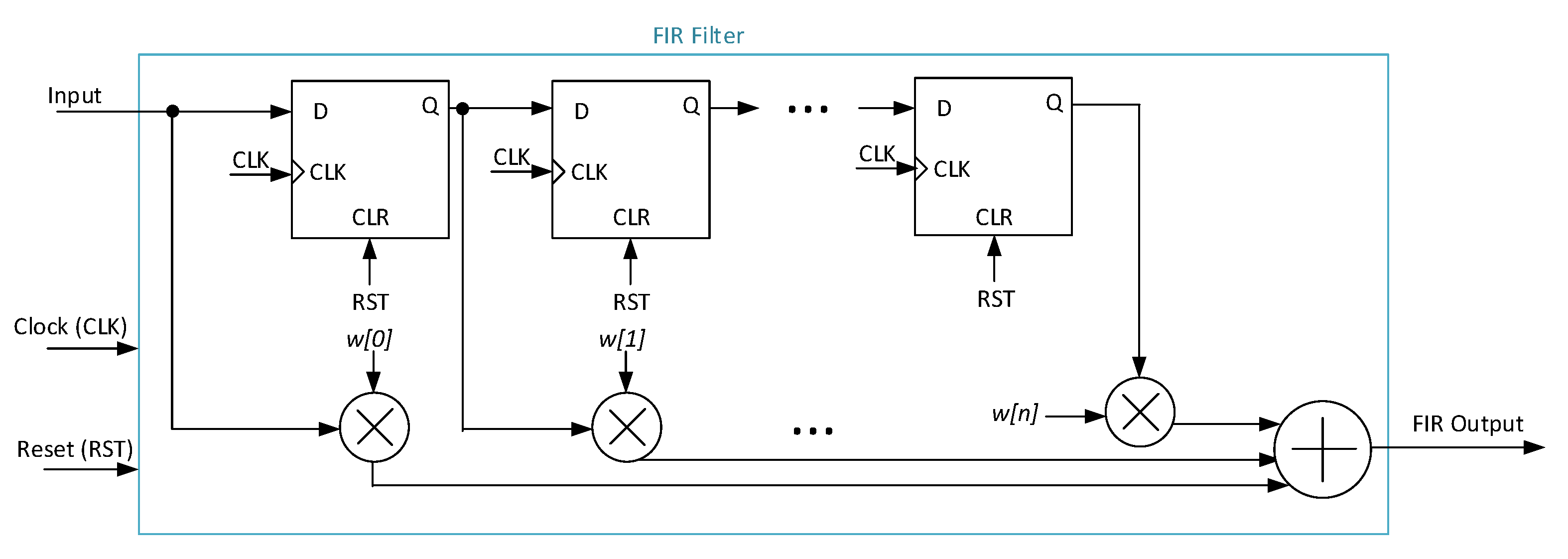
Figure 14.
Impulse Responses for CSP and PSC stages.
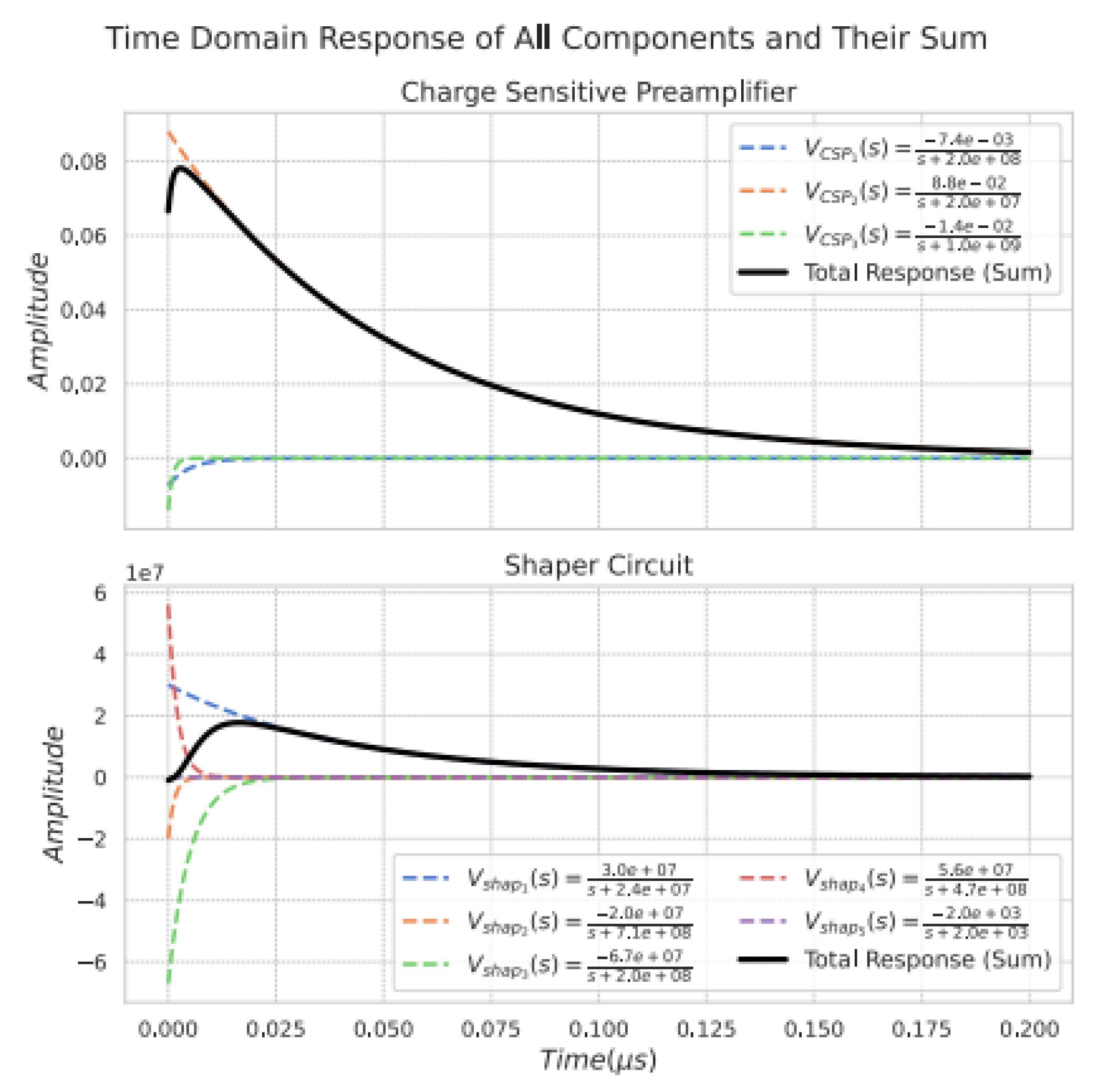
Figure 15.
Impulse Response of CSP and PSC stages combined.
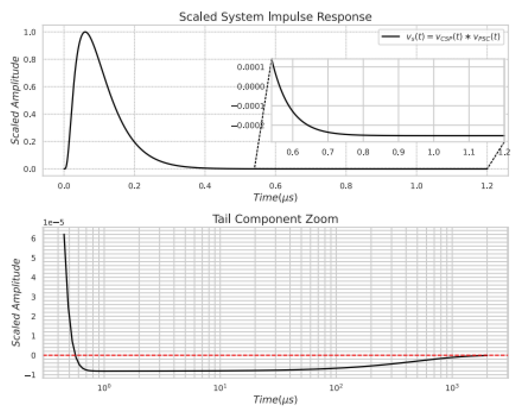
Figure 16.
Pole Zero Map.
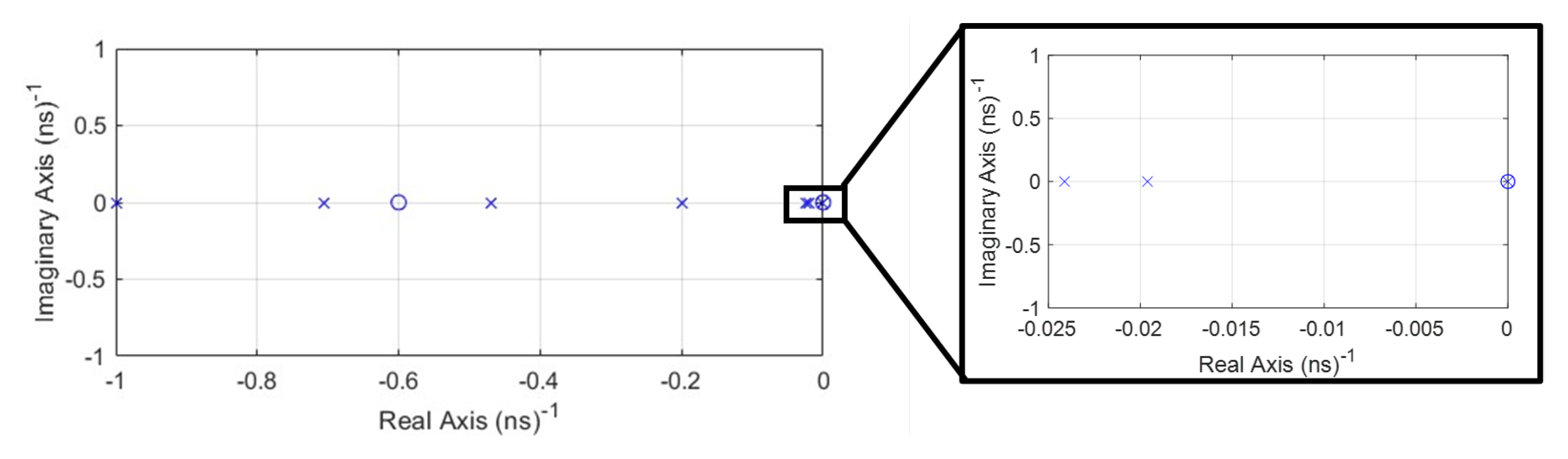
Figure 17.
Baseline shift level as a function of event rate.
Disclaimer/Publisher’s Note: The statements, opinions and data contained in all publications are solely those of the individual author(s) and contributor(s) and not of MDPI and/or the editor(s). MDPI and/or the editor(s) disclaim responsibility for any injury to people or property resulting from any ideas, methods, instructions or products referred to in the content. |
© 2024 by the authors. Licensee MDPI, Basel, Switzerland. This article is an open access article distributed under the terms and conditions of the Creative Commons Attribution (CC BY) license (http://creativecommons.org/licenses/by/4.0/).
Copyright: This open access article is published under a Creative Commons CC BY 4.0 license, which permit the free download, distribution, and reuse, provided that the author and preprint are cited in any reuse.


