Submitted:
03 December 2024
Posted:
04 December 2024
You are already at the latest version
Abstract
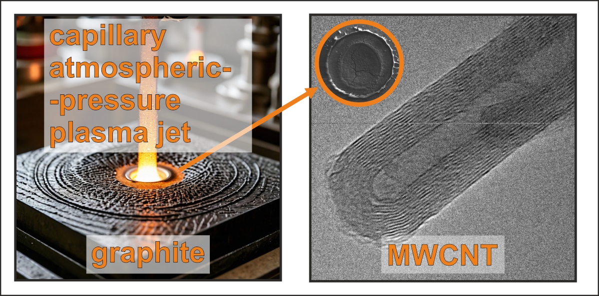
We report the formation of multi-walled carbon nanotubes (MWCNTs) through the interaction of an atmospheric-pressure plasma jet, generated via a capillary discharge, with a graphite surface. This surface-modifying discharge was established in a brief air gap between the cathode and ignition electrode, manipulated across varying discharge power levels. Notably, the structural properties of MWCNTs on the graphite anodes demonstrated a clear dependence on discharge power. Utilizing scanning electron microscopy, transmission electron microscopy, and Raman spectroscopy, we observed a progression toward disordering in the nanotubes alongside the emergence of graphitized clusters with increasing discharge energy. The formation of relatively defect-free MWCNTs at minimal discharge energy presents an opportunity for their synthesis with low energy consumption of 4.7 kJ/cm2. The suggested energy-efficient, rapid and straightforward technique for tailoring MWCNT formation significantly reduces the reliance on complex and expensive instrumentation, presenting a promising pathway for effective surface modification with potential applications in electronics, gas sensors, and water treatment.
Keywords:
plasma surface modification
; carbon nanotubes vibrational spectroscopy
; carbon nanotubes disordering
; precursor-free carbon nanotube synthesis
; precursor-free MWCNT
1. Introduction
The quest for versatile nanomaterials has accelerated interest in carbon-based structures, particularly multi-walled carbon nanotubes (MWCNTs), due to their exceptional mechanical, electrical, and thermo-physical properties [1,2,3]. The unique properties of MWCNTs make them candidate materials for a myriad of applications, including but not limited to nanoscale electronics, biomedical devices, sensors, energy storage and environmental remediation technologies [4,5,6,7,8]. Hence, the development of efficient synthesis methods that can produce high-quality MWCNTs is a critical endeavor in materials science.
Traditional methods for synthesizing MWCNTs, such as catalytic chemical vapor deposition (CVD) [9], arc discharge [10], and pyrolysis [11], often involve complex operating conditions, high material costs, and specialized equipment. These limitations have prompted researchers to seek alternative methods that leverage more accessible and cost-effective techniques. Among these, the use of atmospheric pressure plasma jets (APPJs) has emerged as a promising avenue for MWCNT synthesis [12,13,14].
The capillary discharge setup involves a short air gap between electrodes, enabling the generation of a plasma jet under atmospheric conditions without the need for vacuum environments. This innovative approach offers the potential for real-time surface modification and material synthesis, making it a viable alternative to conventional methods [12]. However, previously-reported approaches either used prefabricated MWCNT paste to be sintered via APPJ [12] or utilized hydrocarbon precursor gases to initiate CVD process [13,14]. In contrast, MWCNT synthesis technique reported in the current study doesn’t require any gas inlet, employing the graphite substrate as a carbon source for MWCNT production.
Thus, we investigate the formation of MWCNTs through the interaction of capillary discharge-based plasma jets in the ambient atmosphere with the surface of graphite substrates. By varying discharge power levels, we explore the influence of plasma treatment on nanotube structure and surface morphology. Our findings indicate a clear relationship between discharge energy and the characteristics of the synthesized MWCNTs, evidenced by morphological transitions and structural disordering as characterized through a combination of scanning electron microscopy (SEM), transmission electron microscopy (TEM), and Raman spectroscopy. By establishing a rapid, efficient, and cost-effective method for the synthesis of MWCNTs, we contribute to the ongoing quest for scalable nanomaterial production techniques. The plasma treatment method described herein opens new avenues for the development of multifunctional nanomaterials suitable for a wide array of technological applications. Thus, this work lays the groundwork for future explorations into atmospheric-pressure plasma techniques in nanotechnology and materials science.
2. Materials and Methods
2.1. Samples Preparation
For this study, cylindrical MPG-6 graphite plates (JSC “Graphi”, Moscow, Russia) with a diameter of 6 mm and a thickness of 2 mm were employed as initial samples to investigate the effects of the capillary discharge jet. These plates were positioned as the lower electrode within the plasmatron, with the capillary applied from above. Consequently, circular regions with a diameter of 2 mm — corresponding to the capillary’s diameter — were subjected to the plasma generated by the capillary discharge. The plasma generator operated at three distinct energy levels: 150, 900, and 4500 J. In subsequent discussions, untreated samples will be referred to as “MPG-6,” while those exposed to the variable-energy atmospheric-pressure plasma jet (AAPJ) will be designated as “150 J,” “900 J,” and “4500 J,” respectively. The discharge power was adjusted by changing the C1 capacity from 3200 μF to 100,000 μF.
A capillary plasmatron setup was utilized for the generation of the plasma jet [15,16]. The schematic representation of the plasma jet generation is illustrated in Figure 1(a). This configuration comprises an ignition capacitor, a switch, a capacitor bank with a discharge device, and electrodes separated by a dielectric, along with a capillary tube.
A discharge was generated using a capillary made of organic glass (polymethyl methacrylate, PMMA) with a diameter of 2 mm and a length of 4 mm. The lower electrode was constructed from MPG-6 graphite, while the upper electrode was made of steel; the other components of the plasmatron were also fabricated from PMMA. The plasmatron was initiated using a G5-15 pulse generator. Initially, the storage capacitor was charged from a power supply to 300 V, a voltage at which self-breakdown of the capillary was not observed. At a designated moment, a high-voltage triggering pulse was delivered via the synchronization system, leading to the breakdown of the capillary. This breakdown allowed the storage capacitor to discharge through the capillary, thereby generating a plasma channel. The increase in current resulted in the heating of the plasma within the capillary, which could lead to the vaporization of the capillary walls as well as the material of the lower electrode. The vaporized substance then entered the discharge volume, where it was heated and ionized. Consequently, the pressure within the capillary rose, resulting in the formation of a plasma jet at the exit of the capillary. The APPJ operation was carried out in ambient conditions, relative humidity was 20%, and no gas inlet was employed.
The duration of the capillary plasmatron pulse was 7 ms, with the voltage across the discharge gap reaching 300 V. The energy varied within the range of 150 - 4500 J, while the peak current during the pulse was 60 - 100 A.
An assessment of the temperature and electron density distribution in the plasma jet generated by the plasmatron using an organic glass capillary is presented in reference [17]. This study demonstrated that the electron density varied along the discharge axis within the range of (1016 - 1018 cm-3), while in the radial direction, it ranged from (1015 - 1017 cm-3). In [17], the axial temperature distribution in the plasma jet was observed to be between 5000 and 6000 K, whereas the radial temperature distribution (at a radius of 6 mm) was found to be in the range of 4000 to 6000 K. Thus, in the plasmatron applied in current study, the plasma temperature changes only slightly, in contrast to the electron density. Typical dynamics of the voltage and current throughout the pulse are presented in Fig. 2(b).
2.2. Sample Characterization
Scanning electron microscopy (SEM) studies were carried out by LEO 1455 VP microscope (Carl Zeiss, Jena, Germany). The accelerating voltage was 10 kV. Detection of secondary electrons was carried out via Everhart–Thornley detector. The setup was equipped with a detector allowing us to perform energy-dispersive X-ray spectroscopy (EDX) studies.
Transmission electron microscopy (TEM) studies were carried out via JEM-2100 200 kV transmission electron microscope (JEOL, Akishima, Japan) equipped with an Orius camera (Gatan, Pleasanton, CA, USA) setup. The electron microscopy grids employed in this study featured copper frames with a cell dimension of 40 μm, onto which a thin polymer film (approximately 5 nm in thickness) was deposited on the upper surface. In order to facilitate the transfer of the structures, modified surfaces of graphite substrates were subjected to mechanical pressing against the polymer-coated side of the grids. This interaction was maintained for a duration of 5 to 10 seconds before the samples were removed, ensuring effective adherence of the structures to the grid substrate.
Raman spectra were obtained via Sunshine GE-Raman spectrometer (Changchun New Industries Optoelectronics Tech. Co., Ltd. (CNI), China, Changchun) coupled to a Leitz Wetzlar microscope (Ernst Leitz GmbH, Germany, Wetzlar). The excitation wavelength was 532 nm, and the power was 1 mW. ×50 objective lens (N.A. = 0.85) was used for the spectra acquisition.
3. Results
3.1. Microscopy
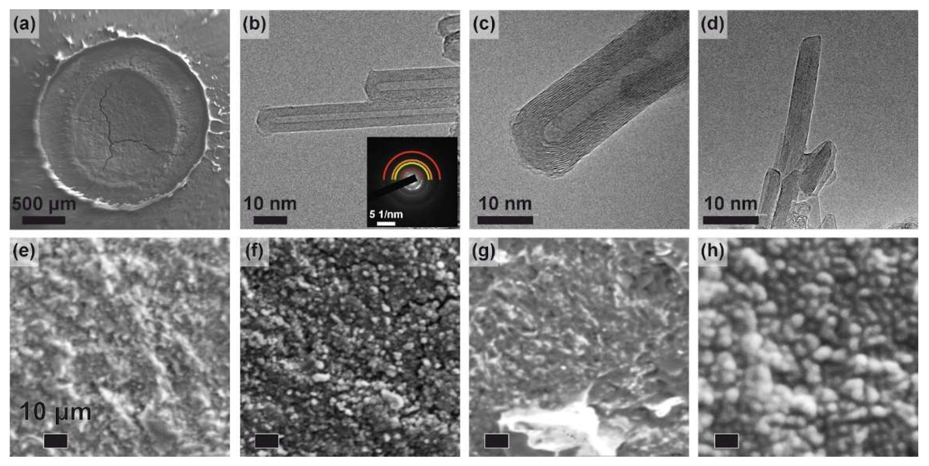
Figure 2(a) displays a survey microphotograph of the surface of the sample before and after exposure to the atmospheric pressure plasma jet. This pattern is characteristic of all studied samples, exhibiting a circular modified area. It consists of a central region where surface-plasma interaction is manifested intensely, surrounded by a ring with an outer diameter corresponding to that of the capillary.
The transmission electron microscopy (TEM) image of the 150 J sample (Fig. 2(b)) illustrates the formation of multi-walled carbon nanotubes (MWCNTs) ranging from 10 to 100 nm in length following atmospheric pressure plasma jet (APPJ) treatment. For 150 J, the radius of the inner core of MWCNT varied within the 2-4 nm range, while the thickness of the CNT layer was within 2.6-5.0 nm, corresponding to 7-14 graphite layers. Nanotube length varied within the 0.1-1 μm range. For 150 J and 900 J samples, similar in shape multi-walled nanotubes were observed, whose length ranged from a few 100 nm to 1 μm (see Fig. 2(b-c)). For samples fabricated at a discharge power of 4500 J, MWCNT shrinking to 100 nm accompanied by its thickness decrease were observed (see Fig. 2(d)).
Selected area electron diffraction (SAED) analysis of the 150 J sample reveals interplanar spacings of 1.2, 1.7, 2.1, and 3.5 Å (see the inset of fig. 2(b)). These diffraction patterns align closely with the established diffraction patterns of MWCNTs, where the identified peaks correspond to the (112), (004), (101), and (002) reflections [18]. Notably, the observed 3.5 Å spacing between graphite layers deviates slightly from the typical value of 3.335 Å. This discrepancy may be attributed to an increase in interlayer distance associated with curved graphitic structures [19]. In the current structures, the widening of the interplanar spacing can be ascribed to both the curvature of the nanotube cappings and distortions within the nanotubes themselves.
To evaluate the morphological changes induced by plasma treatment on the carbon surface, close-up SEM images were analyzed (Fig. 2(e-h)). For the non-irradiated MPG-6 samples, the surface exhibited a relatively coarse texture, with protruding morphological features typically ranging from 10 to 100 μm in size, as displayed in Fig. 2(e). Treatment with a 150 J APPJ reduced the density of larger protruding features and facilitated the formation of small globular grains, measuring 1-5 μm in diameter, as indicated in Fig. 1(f). Increasing the energy input to 900 J led to the emergence of larger faceted grains, sized between 10 and 100 μm, alongside a coarsening of the surface, as shown in Fig. 2(g). A high-energy treatment at 4500 J resulted in a complete reconfiguration of the surface, culminating in the agglomeration of globular features (fig. 2(h)). This observed trend bears some resemblance to findings from arc plasma treatments of graphite [20]. In the referenced study, an increase in treatment time facilitated the transition from small globular nanotube clusters to irregular agglomerated “lumps”; however, further increases in irradiation dose resulted in the formation of larger globules. While arc plasma treatment of graphite enables the production of MWCNTs on a 2 cm x 2 cm disc, compared to the 0.2 cm x 0.2 cm under-capillary area modified in the present study, it necessitates a complex setup, including an arc plasma reactor with an argon inlet. Moreover, the arc energy required to process the graphite sample exceeds 5.5 MJ, surpassing the energy consumption of the atmospheric pressure plasma jet (APPJ) by 3 to 4 orders of magnitude. Consequently, we regard APPJ treatment as a more straightforward and energy-efficient method for MWCNT formation whose energy consumption is as low as 4.7 kJ/cm2. These results corroborate with previous studies of carbon nanotubes synthesis via APPJ revealing the energy requirement of 500 J/cm2 [12]. However, unlike [12], our technique doesn’t require a complicated deposition setup including gas inlet and surface pre-treatment.
3.2. EDX
The elemental analysis of all samples revealed carbon and oxygen compositions of 93.8 ± 1 at.% and 6.2 ± 0.6 at.%, respectively. Notably, during exposure to capillary discharge plasma at varying power levels, the elemental composition of the irradiated samples exhibited negligible alterations from untreated MPG-6 graphite, remaining invariant within a margin of 1%.
3.3. Raman Spectroscopy
In Fig. 2(a), we present the background-subtracted Raman spectra. Spectra were normalized to similar intensity, and vertical offset is applied to distinguish the lines. Untreated MPG-6 shows the four-component spectrum which is typical for hard graphitic carbon [21]. In this spectrum, 1360 cm-1 band is assigned to D-line, which is attributed to the breathing mode of graphitic rings active in the presence of disorder; 1596 cm-1 is ascribed to G-line, which is assigned to the stretching vibrations of C=C bonds [22]. Less intensive 1231 cm-1 and 1480 cm-1 lines are ascribed to the stretching vibrations of polyene-like C-C and C=C bonds [23,24]. Manifestation of these lines is supposedly caused by the vibrations of conjugated polymer fragments-based contaminations.
Figure 3.
Energy-dependent variation of the vibrational signature and structure. (a) Background-subtracted Raman spectra. Numbers indicate the line positions. Black line indicates experimental data, colored lines indicate fitted spectra components and their sum (envelope). (b) Illustration of the energy-dependent structural changes.
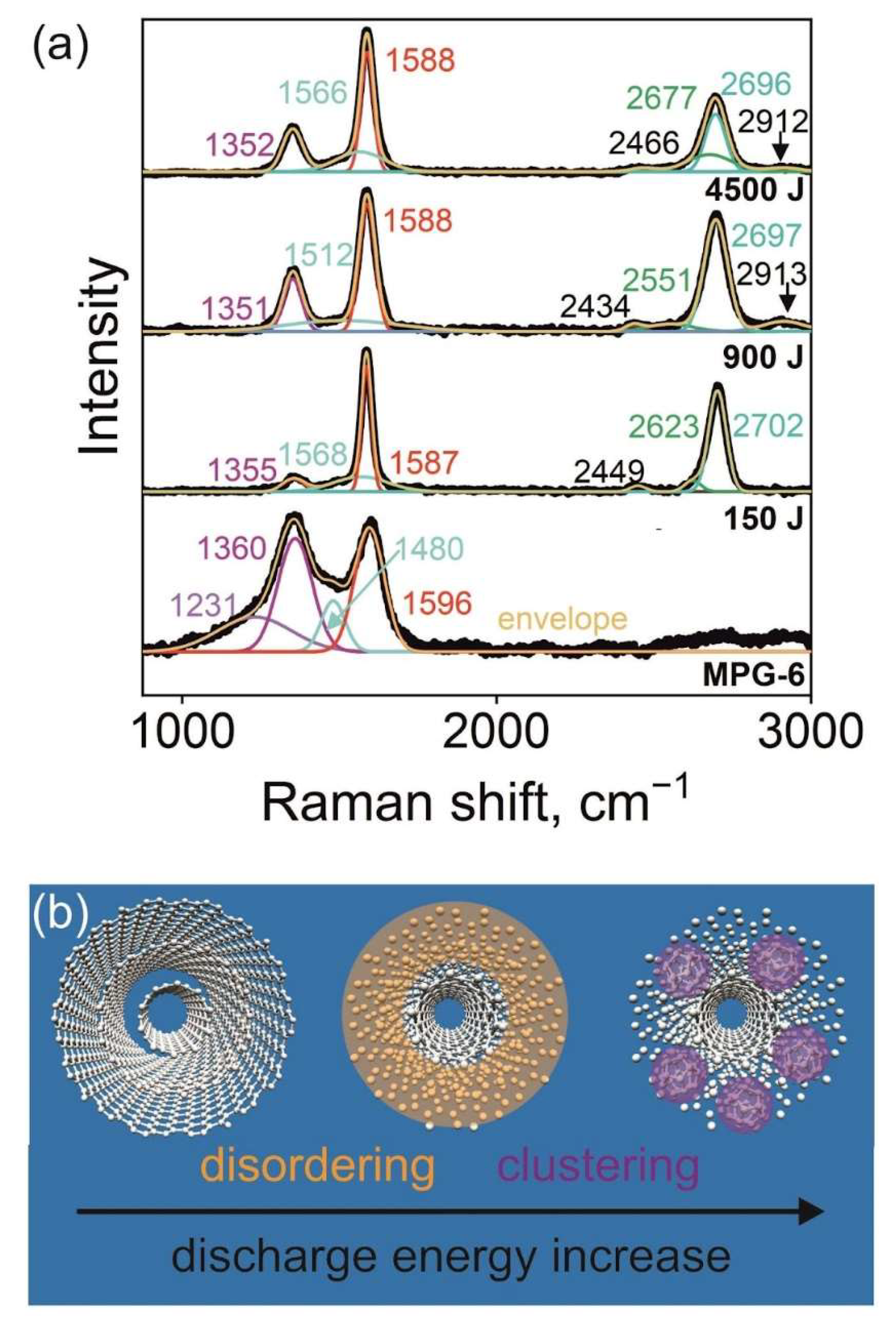
Spectra of APPJ-treated samples show lines at 1351-1355 cm-1 (peak 1, violet-colored line in Fig.2(a)), 1512-1568 cm-1 (peak 2, turquoise line), 1587-1588 cm-1 (peak 3, red line), 2434-2466 cm-1 (peak 4, black line), 2551-2677 cm-1 (peak 5, green line), 2696-2702 cm-1 (peak 6, turquoise line), and 2912-2913 cm-1 (peak 7, black line). Peaks 1 and 3 are attributed to D- and G-lines of nanotubes, while significant width of peak 2 is ascribed to C=C vibrations of amorphous carbon (a-C) component. Somewhat similar splitting of the G-line to “structure-related” and “disorder-related” component was previously observed for ion-irradiated polyene-polyyne materials [22]. Low-intensity peak 4 originates from the two-phonon double resonance process mode taking place in carbon nanotubes and graphene [25]. Intensive peak 6 is a G’ band also caused by two-phonon resonance, i.e. overtone of D mode manifesting in carbon nanotubes and graphene. Peak 5 -- a shoulder of G’ band -- is also ascribed to D mode overtone -- but its position is rather typical for single-wall carbon nanotubes [26,27]. Its manifestation indicates that some small fraction of nanotubes present in the samples is atomically thin. Peak 7 is assigned to D+G peak [28].
Overall spectra are typical for MWCNT [29], however, a considerable change of line positions and shapes is observed with discharge energy variation. APPJ-induced MWCNT disordering and amorphization should be considered to address the changes in the vibrational signature of the MWCNT-based samples. Increase of the discharge energy from 150 to 900 J led to the increase of the width of G-band from 37 to 60 cm-1 (line 3) and simultaneous rise of the ID/IG parameter (D-band to G-band intensity ratio) from 0.23 to 0.46, which indicates the material disordering [30]. However, subsequent energy increase from 900 J to 4500 J didn’t result in further amorphization, which is indicated by 4500 J G-line width of 47 cm-1 and ID/IG of 0.56 differing only slightly from the parameters of 900 J sample. However, for this sample we observe the rise of the relative intensity of the line 2 indicative of the disordered carbon component. Its emergence indicates that high discharge energy led to the formation of graphitic clusters from irradiated nanotube phase, i.e. amorphisation of the MWCNTs. Gradual decrease of the D’-band intensity (ID’/IG = 1.43 for 150 J, 1.27 for 900 J, 0.77 for 4500 J) confirms the suggested MWCNT degradation model. As D’ is sensitive to defects [31] and amorphous carbon content does not contribute to its intensity, both disordering and amorphisation lead to its suppression with energy. Structural modifications derived from the vibrational signature of the material are schematically represented in Fig. 3b.
4. Discussion
4.1. APPJ Effect on the Structure
On the surface of all APPJ-treated samples, SEM examination revealed a circular pattern consisting of a central area where plasma-substrate interaction was most intensive, surrounded by a ring with an outer diameter equal to that of the capillary. According to data from TEM and Raman spectroscopy, MWCNTs were formed across all reported discharge regimes. Notably, at a discharge energy of 150 J, the formation of relatively defect-free nanotubes was observed. The nanotube formation is primarily attributed to the harsh conditions of capillary discharge, characterized by intense heating (up to 5000–6000 K) and high concentrations of ionized particles. The dense flow of capillary discharge predominantly impacts the surface of the graphite substrate, thereby inducing structural and morphological transformations. Previous studies indicated that carbon nanotube formation in plasma occurred under discharge pressures exceeding 20 kPa, as reported in Ref. [32], which is corroborated by the current study.
Upon increasing the pulse energy to 900 J, the average parameters and shapes of the nanotubes remained unchanged; however, SEM analysis indicated modifications in surface morphology associated with grain agglomeration, indicating a prominent discharge-induced surface diffusion. The Raman spectra showed an increase in the intensity of the D-line, suggesting an enhancement in the disorder degree of the nanotubes, likely related to the formation of a greater number of defects due to the dense flow of charged particles (1015–1018 cm-3) in higher power plasma. Further increasing the power (up to 4500 J) led to additional surface restructuring, resulting in the formation of globular particles. Overall, the observed changes in the morphological characteristics of the sample surfaces with varying discharge power may be attributed to both the influence of high-density plasma and the effects of high-temperature exposure, leading to textural and structural alterations in the samples.
4.2. Potential Applications of APPJ-Produced Nanotubes
The atmospheric-pressure plasma jet (APPJ) technique developed in this study for synthesizing multi-walled carbon nanotubes (MWCNTs) presents a promising platform for novel applications across various fields, including field-emission displays, energy storage, water treatment, electronic components and sensing elements. The inherent advantages of MWCNTs — particularly, their high surface area, electrical and heat conductance — make them suitable candidates for enhancing performance in these domains.
Delving deeper into the realm of nanotube applications, we denote that MWCNT are increasingly recognized for their role in field-emission devices, attributed to their low threshold voltage, extended lifespan, high brightness, and coherent electron emission characteristics [33]. These attributes render MWCNTs particularly promising candidates for components in field-emission displays [34]. Despite the slowdown in developing nanotube-based displays in light of the rapid evolution of LED and OLED technologies, ongoing research into the utility of nanotubes as cathodes remains robust [34,35,36].
Additionally, the growing demand for efficient energy storage systems drives research into advanced materials for battery electrodes. MWCNTs, with their high aspect ratio and excellent electrical conductivity, can significantly improve the performance of electrochemical cells [37,38]. In lithium-ion batteries, for example, the incorporation of MWCNTs into anodes can lead to enhanced cycling stability and capacity retention, thus addressing one of the main drawbacks of conventional graphite electrodes.
Besides, the enlistment of MWCNTs in water treatment technologies, particularly desalination processes, presents an exciting frontier. Given their high surface area and porous nature, MWCNTs have the potential to function as efficient adsorbents for contaminants found in saline water and wastewater [39,40,41,42].
Moreover, the versatility of APPJ-synthesized MWCNTs also extends into the realm of electronics, where local modifications of electrophysical and thermal properties can be achieved. Tunable electrical and heat conductivity of MWCNTs enables targeted enhancements in electronic circuits, where specific regions can be selectively modified to optimize performance. In addition, MWCNT can be used to obtain effective gas sensors [43]. The sensitivity and selectivity of resistive vapor sensors is paramount for the detection of volatile organic compounds (VOCs) and hazardous gases. MWCNTs, with their high surface area and affinity for electron-donor molecules, such as ammonia [22], can enhance the response characteristics of resistive sensors.
5. Conclusions
This study demonstrates a novel and energy-efficient method for synthesizing MWCNTs via atmospheric-pressure plasma jets generated by capillary discharge. Our findings indicate that the structural properties of MWCNTs formed on graphite substrates are significantly influenced by the discharge energy, leading to variations in morphology and disorder of nanotubes. At lower discharge power level, we successfully synthesized relatively defect-free MWCNTs, which allowed for the surface modification with an energy consumption of just 4.7 kJ/cm2. As discharge energy increased, we observed a rise in structural disorder and the formation of graphitized clusters, suggesting a transition from well-ordered to disordered structure.
The energy-effective possibility to obtain MWCNT via APPJ technique facilitates real-time surface modifications for various applications across electronics, environmental technology, and energy storage systems. The simplicity and cost-effectiveness of the proposed methodology make it a compelling alternative to more complex synthesis techniques, such as catalytic chemical vapor deposition, arc discharge, and pyrolysis.
Our work lays the groundwork for future research in the area of atmospheric-pressure plasma applications in nanotechnology, offering pathways for designing multifunctional nanomaterials tailored for specific technological needs. The ability to control MWCNT properties through plasma parameters opens new horizons for material research and industrial applications, addressing the growing demand for high-performance, low-cost nanomaterials.
Author Contributions
Conceptualization, Vladimir Bychkov and Oleg Streletskiy; Data curation, Ilya Zavidovskiy; Formal analysis, Ilya Zavidovskiy; Funding acquisition, Ilya Zavidovskiy; Investigation, Vladimir Baidak and Andrey Tatarintsev; Methodology, Oleg Streletskiy; Project administration, Oleg Streletskiy; Resources, Andrey Tatarintsev and Oleg Streletskiy; Supervision, Vladimir Bychkov; Validation, Vladimir Baidak; Visualization, Ilya Zavidovskiy; Writing – original draft, Ilya Zavidovskiy; Writing – review & editing, Oleg Streletskiy.
Funding
The research was funded by the Russian Science Foundation (project № 24-22-00152, https://rscf.ru/project/24-22-00152/).
Conflicts of Interest
The authors declare no conflicts of interest.
References
- Mechanical Properties of Carbon Nanotubes (CNTs): A Review. EAJSE 2022, 8. [CrossRef]
- Lee, J.; Lim, H.; Ha, J.; Lee, S.; Lee, H. Structural Analysis and Electrical Property of Acid-Treated MWCNT. Surface & Interface Analysis 2024, 56, 851–857. [Google Scholar] [CrossRef]
- Bobenko, N.; Egorushkin, V.; Ponomarev, A. Hysteresis in Heat Capacity of MWCNTs Caused by Interface Behavior. Nanomaterials 2022, 12, 3139. [Google Scholar] [CrossRef] [PubMed]
- Jindal, P.K.; Sandha, K.S. Influence of Variable Temperature on Performance of Mixed-MWCNT, MWCNT and SWCNT Nanostructures as Interconnects for High-Performance VLSI-IC Design. J Mater Sci: Mater Electron 2020, 31, 1828–1838. [Google Scholar] [CrossRef]
- Kotzabasaki, M.; Sotiropoulos, I.; Charitidis, C.; Sarimveis, H. Machine Learning Methods for Multi-Walled Carbon Nanotubes (MWCNT) Genotoxicity Prediction. Nanoscale Adv. 2021, 3, 3167–3176. [Google Scholar] [CrossRef] [PubMed]
- Karimi-Maleh, H.; Cellat, K.; Arıkan, K.; Savk, A.; Karimi, F.; Şen, F. Palladium–Nickel Nanoparticles Decorated on Functionalized-MWCNT for High Precision Non-Enzymatic Glucose Sensing. Materials Chemistry and Physics 2020, 250, 123042. [Google Scholar] [CrossRef]
- Briceño, J.; Rosas, D.; Lemus, I.L.A.-; Barbosa, R.; Escobar, B. Green Synthesis of N-Doped MWCNTs via Simple Modification of CVD Technique and Evaluation of Its Viability as an Electrode in AEMFC. Journal of Analytical and Applied Pyrolysis 2023, 174, 106082. [Google Scholar] [CrossRef]
- Moses, H.; Odigure, J.O.; Otaru, A.J.; Oduoza, C.F. A Potential Remediation of Total Petroleum Hydrocarbon from Contaminated Soils Using Surfactant Suspended Multiwall Carbon Nanotubes. Results in Engineering 2023, 19, 101371. [Google Scholar] [CrossRef]
- Skudin, V.; Andreeva, T.; Myachina, M.; Gavrilova, N. CVD-Synthesis of N-CNT Using Propane and Ammonia. Materials 2022, 15, 2241. [Google Scholar] [CrossRef]
- Zain Mehdi, S.M.; Shin, T.H.; Abbas, S.Z.; Kwon, H.; Seo, Y.; Kim, D.; Hong, S.J.; Goak, J.C.; Lee, N. Superior Field Emission Characteristics of Highly Crystalline and Thermally Stable Carbon Nanotubes Grown in N2 and O2 by Arc Discharge. Ceramics International 2023, 49, 4668–4676. [Google Scholar] [CrossRef]
- Veksha, A.; Lu, J.; Tsakadze, Z.; Lisak, G. Carbon Dioxide Capture from Biomass Pyrolysis Gas as an Enabling Step of Biogenic Carbon Nanotube Synthesis and Hydrogen Recovery. ChemSusChem 2023, 16, e202300143. [Google Scholar] [CrossRef] [PubMed]
- Chen, J.-Z.; Wang, C.; Hsu, C.-C.; Cheng, I.-C. Ultrafast Synthesis of Carbon-Nanotube Counter Electrodes for Dye-Sensitized Solar Cells Using an Atmospheric-Pressure Plasma Jet. Carbon 2016, 98, 34–40. [Google Scholar] [CrossRef]
- Nozaki, T.; Yoshida, S.; Karatsu, T.; Okazaki, K. Atmospheric-Pressure Plasma Synthesis of Carbon Nanotubes. J. Phys. D: Appl. Phys. 2011, 44, 174007. [Google Scholar] [CrossRef]
- Lee, K.H.; Jang, H.-S.; Eom, G.-Y.; Lee, B.-J.; Burk, D.; Overzet, L.; Lee, G.S. The Enhanced Growth of Multi-Walled Carbon Nanotubes Using an Atmospheric Pressure Plasma Jet. Materials Letters 2008, 62, 3849–3851. [Google Scholar] [CrossRef]
- Bychkov, V.L.; Chernikov, V.A.; Osokin, A.S.; Stepanov, A.I.; Stepanov, I.G. Modeling of Artificial Ball Lightning With a Help of Capillary Discharge. IEEE Trans. Plasma Sci. 2015, 43, 4043–4047. [Google Scholar] [CrossRef]
- Bychkov, V.L. Ball Lightning With a Cover Filled by a Vapor. IEEE Trans. Plasma Sci. 2014, 42, 3912–3915. [Google Scholar] [CrossRef]
- Ершoв, А.П.; Рoзанoв, В.В.; Сысoев, Н.Н.; Тимoфеев, И.Б.; Чувашев, С.Н.; Шибкoв, В.М. ИСТЕКАЮЩИЕ В АМТОСФЕРУ ДОЗВУКОВЫЕ ПЛАЗМЕННЫЕ СТРУИ, ОБРАЗУЕМЫЕ КАПИЛЛЯРНЫМ РАЗРЯДОМ. 1995, 36–51.
- Corrias, A.; Mountjoy, G.; Gozzi, D.; Latini, A. Multi-Walled Carbon Nanotubes Decorated with Titanium Nanoparticles: Synthesis and Characterization. Nanotechnology 2007, 18, 485610. [Google Scholar] [CrossRef]
- Dai, D.; Li, Y.; Fan, J. Room-Temperature Synthesis of Various Allotropes of Carbon Nanostructures (Graphene, Graphene Polyhedra, Carbon Nanotubes and Nano-Onions, n-Diamond Nanocrystals) with Aid of Ultrasonic Shock Using Ethanol and Potassium Hydroxide. Carbon 2021, 179, 133–141. [Google Scholar] [CrossRef]
- Nayak, B.B.; Sahu, R.K.; Dash, T.; Pradhan, S. Growth of Carbon Nanotubes in Arc Plasma Treated Graphite Disc: Microstructural Characterization and Electrical Conductivity Study. Appl. Phys. A 2018, 124, 220. [Google Scholar] [CrossRef]
- Wu, Q.; Shu, K.; Zhao, L.; Zhang, J. Pomegranate Peel-Derived Hard Carbons as Anode Materials for Sodium-Ion Batteries. Molecules 2024, 29, 4639. [Google Scholar] [CrossRef]
- Zavidovskiy, I.A.; Streletskiy, O.A.; Nuriahmetov, I.F.; Nishchak, O.Y.; Savchenko, N.F.; Tatarintsev, A.A.; Pavlikov, A.V. Highly Selective Polyene-Polyyne Resistive Gas Sensors: Response Tuning by Low-Energy Ion Irradiation. Journal of Composites Science 2023, 7, 156. [Google Scholar] [CrossRef]
- Streletskiy, O.A.; Zavidovskiy, I.A.; Nishchak, O.Yu.; Khaidarov, A.A.; Savchenko, N.F.; Pavlikov, A.V. Low-Threshold Field Emission Cathode Based on Heat-Treated Dehydrofluorinated Polyvinylidene Fluoride. J. Exp. Theor. Phys. 2022, 135, 844–852. [Google Scholar] [CrossRef]
- Zavidovskiy, I.A.; Streletskiy, O.A.; Nishchak, O.Yu.; Haidarov, A.A.; Pavlikov, A.V. The Influence of Ion Assistance Energy on Structural and Optical Properties of Carbon-Silver Nanocomposites. Thin Solid Films 2021, 738, 138966. [Google Scholar] [CrossRef]
- Shimada, T.; Sugai, T.; Fantini, C.; Souza, M.; Cançado, L.G.; Jorio, A.; Pimenta, M.A.; Saito, R.; Grüneis, A.; Dresselhaus, G.; et al. Origin of the 2450cm−1 Raman Bands in HOPG, Single-Wall and Double-Wall Carbon Nanotubes. Carbon 2005, 43, 1049–1054. [Google Scholar] [CrossRef]
- Heise, H.M.; Kuckuk, R.; Srivastava, A.; Asthana, B.P. Characterization of Carbon Nanotube Filters and Other Carbonaceous Materials by Raman Spectroscopy—II: Study on Dispersion and Disorder Parameters. J Raman Spectroscopy 2011, 42, 294–302. [Google Scholar] [CrossRef]
- Mussi, V.; Biale, C.; Visentin, S.; Barbero, N.; Rocchia, M.; Valbusa, U. Raman Analysis and Mapping for the Determination of COOH Groups on Oxidized Single Walled Carbon Nanotubes. Carbon 2010, 48, 3391–3398. [Google Scholar] [CrossRef]
- Vollebregt, S.; Ishihara, R.; Tichelaar, F.D.; Hou, Y.; Beenakker, C.I.M. Influence of the Growth Temperature on the First and Second-Order Raman Band Ratios and Widths of Carbon Nanotubes and Fibers. Carbon 2012, 50, 3542–3554. [Google Scholar] [CrossRef]
- Heise, H.M.; Kuckuk, R.; Ojha, A.K.; Srivastava, A.; Srivastava, V.; Asthana, B.P. Characterisation of Carbonaceous Materials Using Raman Spectroscopy: A Comparison of Carbon Nanotube Filters, Single- and Multi-walled Nanotubes, Graphitised Porous Carbon and Graphite. J Raman Spectroscopy 2009, 40, 344–353. [Google Scholar] [CrossRef]
- Keshtmand, R.; Khanlary, M.-R.; Keshtmand, Z. Radiation Damage to Multi-Walled Carbon Nanotubes and Their Raman Vibrational Modes. Bull Mater Sci 2015, 38, 1771–1775. [Google Scholar] [CrossRef]
- Bobenko, N.G.; Bolotov, V.V.; Egorushkin, V.E.; Korusenko, P.M.; Melnikova, N.V.; Nesov, S.N.; Ponomarev, A.N.; Povoroznyuk, S.N. Experimental and Theoretical Study of Electronic Structure of Disordered MWCNTs. Carbon 2019, 153, 40–51. [Google Scholar] [CrossRef]
- Nozaki, T.; Okazaki, K. Carbon Nanotube Synthesis in Atmospheric Pressure Glow Discharge: A Review. Plasma Processes & Polymers 2008, 5, 300–321. [Google Scholar] [CrossRef]
- Laszczyk, K.U. Field Emission Cathodes to Form an Electron Beam Prepared from Carbon Nanotube Suspensions. Micromachines 2020, 11, 260. [Google Scholar] [CrossRef] [PubMed]
- Kuznetzov, A.A.; Lee, S.B.; Zhang, M.; Baughman, R.H.; Zakhidov, A.A. Electron Field Emission from Transparent Multiwalled Carbon Nanotube Sheets for Inverted Field Emission Displays. Carbon 2010, 48, 41–46. [Google Scholar] [CrossRef]
- Kleshch, V.I.; Eremina, V.A.; Serbun, P.; Orekhov, A.S.; Lützenkirchen-Hecht, D.; Obraztsova, E.D.; Obraztsov, A.N. A Comparative Study of Field Emission From Semiconducting and Metallic Single-Walled Carbon Nanotube Planar Emitters. Physica Status Solidi (b) 2018, 255, 1700268. [Google Scholar] [CrossRef]
- Tang, H.; Liu, R.; Huang, W.; Zhu, W.; Qian, W.; Dong, C. Field Emission of Multi-Walled Carbon Nanotubes from Pt-Assisted Chemical Vapor Deposition. Nanomaterials 2022, 12, 575. [Google Scholar] [CrossRef]
- Chen, Y.; Li, F.; Tang, D.-M.; Jian, Z.; Liu, C.; Golberg, D.; Yamada, A.; Zhou, H. Multi-Walled Carbon Nanotube Papers as Binder-Free Cathodes for Large Capacity and Reversible Non-Aqueous Li–O2 Batteries. J. Mater. Chem. A 2013, 1, 13076. [Google Scholar] [CrossRef]
- Landi, B.J.; Dileo, R.A.; Schauerman, C.M.; Cress, C.D.; Ganter, M.J.; Raffaelle, R.P. Multi-Walled Carbon Nanotube Paper Anodes for Lithium Ion Batteries. J. Nanosci. Nanotech. 2009, 9, 3406–3410. [Google Scholar] [CrossRef]
- Ceroni, L.; Benazzato, S.; Pressi, S.; Calvillo, L.; Marotta, E.; Menna, E. Enhanced Adsorption of Methylene Blue Dye on Functionalized Multi-Walled Carbon Nanotubes. Nanomaterials 2024, 14, 522. [Google Scholar] [CrossRef]
- Kuśmierek, K.; Świątkowski, A.; Skrzypczyńska, K.; Dąbek, L. Adsorptive and Electrochemical Properties of Carbon Nanotubes, Activated Carbon, and Graphene Oxide with Relatively Similar Specific Surface Area. Materials 2021, 14, 496. [Google Scholar] [CrossRef]
- Liu, S.; Wang, L.; Xia, J.; Wang, R.; Tang, C.; Wang, C. Competition between Hydration Shell and Ordered Water Chain Induces Thickness-Dependent Desalination Performance in Carbon Nanotube Membrane. Membranes 2023, 13, 525. [Google Scholar] [CrossRef]
- Zhou, Y.; He, Y.; Wang, R.; Mao, Y.; Bai, J.; Dou, Y. Modification of Multiwalled Carbon Nanotubes and Their Mechanism of Demanganization. Molecules 2023, 28, 1870. [Google Scholar] [CrossRef] [PubMed]
- Grabarczyk, M.; Wardak, C.; Piech, R.; Wawruch, A. An Electrochemical Sensor for the Determination of Trace Concentrations of Cadmium, Based on Spherical Glassy Carbon and Nanotubes. Materials 2023, 16, 3252. [Google Scholar] [CrossRef] [PubMed]
Figure 1.
APPJ discharge: schematics and parameters. (a) The electrical circuit of the capillary plasmatron: 1 marks the discharge unit of the capillary plasmatron; 2 -- graphite cathode and 3 -- ignition electrode, 4 indicates the switch; R1 and R2 are the resistances of the voltage divider; R3 serves as the shunt resistance for discharge current measurement; L is a circuit inductance, C1 denotes the capacitor bank; C2 represents the ignition capacitor. (b) Characteristic discharge dynamics of voltage (black line, left axis) and current (red line, right axis).
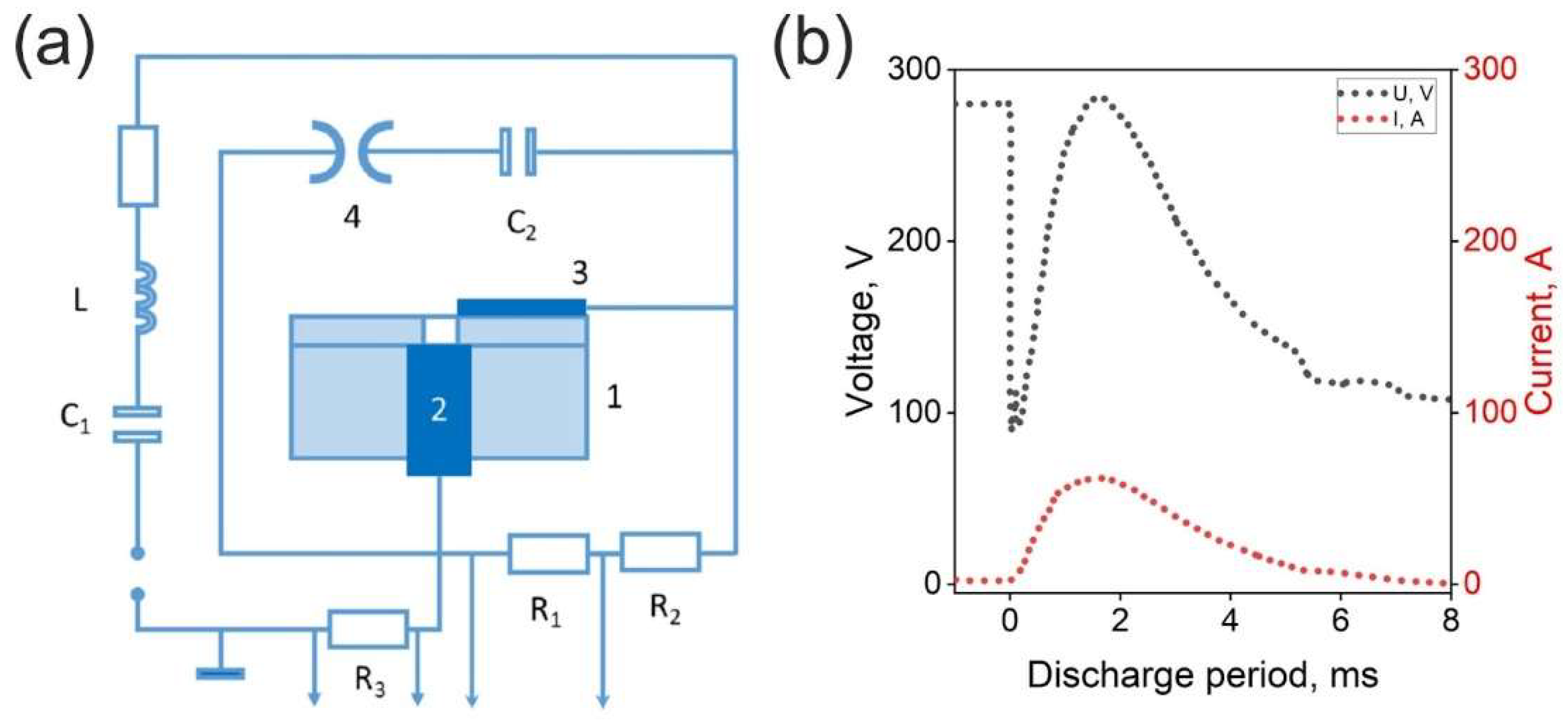
Figure 2.
Morphological characterization. (a) Typical survey SEM image of the graphite area after interaction with APPJ. (b-d) TEM images of 150 J (b), 900 J (c) and 4500 J (d) samples. In the inset of Fig. 2b, SAED pattern of 150 J sample is shown. In the inset, red, orange, yellow and brown arcs denote (112), (004), (101), and (002) reflections, respectively. (e-h) Close-up SEM images: (e) MPG-6; (f) 150 J; (g) 900 J; (h) 4500 J. In (e-h), the scale bar length is 10 μm.
Disclaimer/Publisher’s Note: The statements, opinions and data contained in all publications are solely those of the individual author(s) and contributor(s) and not of MDPI and/or the editor(s). MDPI and/or the editor(s) disclaim responsibility for any injury to people or property resulting from any ideas, methods, instructions or products referred to in the content. |
© 2024 by the authors. Licensee MDPI, Basel, Switzerland. This article is an open access article distributed under the terms and conditions of the Creative Commons Attribution (CC BY) license (http://creativecommons.org/licenses/by/4.0/).
Copyright: This open access article is published under a Creative Commons CC BY 4.0 license, which permit the free download, distribution, and reuse, provided that the author and preprint are cited in any reuse.


