
Submitted:
18 November 2024
Posted:
19 November 2024
You are already at the latest version
Abstract
In the present work, the growth specificity of Cd1−xMnxTe layers by the molecular beam epitaxy and results of experimental studies of several Cd1−xMnxTe layers grown on GaAs(100) hybrid substrates with CdTe buffers are presented. Our efforts were concentrated on creating structures with high crystallographic quality, specifically aiming to reduce the number of defects. Experimental results for the selected structures demonstrated that the Cd1−xMnxTe layers, with varying x, exhibit high crystallographic and surface morphology quality. Specifically, high-resolution X-ray diffraction measurements and their analysis revealed that the intensity distribution does not reflect the effects of mosaicity or dislocation density. The aim of the work was to characterize the Mn dopant depending on the x-value. The magnetic properties were studied as a function of manganese concentration by using electron paramagnetic resonance. By applying continuous wave electron paramagnetic resonance in the wide temperature range, we observed two groups of lines: from manganese and from so-called low field magnetic absorption.
Keywords:
CdMnTe
; MBE
; EPR
; magnetic properties
1. Introduction
Cadmium manganese telluride (Cd1-xMnxTe, or in short CdMnTe) belongs to the group of compounds currently being studied for room temperature nuclear detectors. It is also a dilute magnetic semiconductor (DMS), caused by the addition of the ferromagnetic element manganese to CdTe. Due to the presence of the magnetic manganese distributed randomly through the lattice, CdMnTe exhibits some other potentially useful properties, such as giant Faraday rotation, magnetic-field-induced metal-insulator transition and the formation of bound magnetic polarons which have been extensively investigated in the literature [1,2]. These properties of CdMnTe have led to its investigation for a wide variety of applications, including Faraday optical isolators, ultrafast Faraday rotators, infrared detectors, tunable solid state lasers, as well as X- and γ-ray detectors [3,4]. However, there are still a number of unknown factors affecting CdMnTe for use as a radiation detector due to its relative immaturity as a material compared to CdTe and CdZnTe [3,5,6,7]. With the promising properties of CdMnTe for use as a single crystal semiconductor radiation detector, it is of great interest to understand the fundamental properties and limiting factors in the material in order to progress its development as a detector material. There is a great depth of knowledge of the magnetic properties already in existence, but more information is needed on fundamental charge transport and the limiting impurities and compensation schemes appropriate for this specific material [6]. The magnetic properties of Cd1-xMnxTe, which exhibit spontaneous magnetization, were not fully understood. Néel referred to them as non-compensated antiferromagnets, or “ferrimagnets" [11].
In this work at first we describe the structural characterization of Cd1-xMnxTe grown by molecular beam epitaxy method (MBE) using a high resolution X-ray diffractometry (HRXRD) and optical, and confocal microscopy. Although molecular-beam-epitaxy-grown Cd1-xMnxTe crystals have been extensively studied using various experimental techniques, there is still a relative scarcity of electron paramagnetic resonance (EPR) spectroscopy data for this material. Thus, we examined magnetic properties, using a powerful tool which is EPR spectroscopy, which gives a unique possibility to investigate the properties of paramagnetic centres.
2. Results
2.1. Structural Characterization
The structures of CdMnTe were characterized by X-ray diffraction analysis, Nomarski contrast photography, and atomic force microscopy imaging. Cross-sectional schematic views are presented on Figure 1. The crystal quality of the grown CdMnTe films is assessed from 2θ-ω scans as well as the full-width at half maximum (FWHM) of the x-ray double-crystal rocking curve (DCRC). For this purpose, all five structures discussed here were examined by HRXRD - see Figure 2. The same measurement parameters were kept, i.e., step size and counting time equal to 0.0002°/s and 0.3s for 2θ-ω scans and 0.0002°/s and 0.1s for ω-RC scans, respectively. High resolution X-ray diffraction was used to perform a comprehensive crystallographic quality analysis. Measurements were performed in both symmetric reflection 004 and asymmetric reflection 115, with the highest precision due to a resolution of 0.0002°/s. The scope of the study was focused on the CdTe buffer and the CdMnTe layer, allowing a detailed evaluation of their properties. In addition, the X-ray measurements were extended to include an inverse space map (RSM) to obtain more detailed data. These procedures were carried out using symmetric reflection 004 and asymmetric reflection 115, as shown on Figure 3 and Figure 4. By using these advanced mapping techniques, a comprehensive picture of the structure of the materials under study was obtained, allowing a precise assessment of their crystallographic quality.
The dominant diffraction reflection in the analyzed pattern is the peak originating from the CdTe buffer, while a lower intensity peak is attributed to the CdMnTe layer. The angular positions of the points made it possible to determine the lattice mismatch of the structures studied. The values obtained were -17883 ppm, -24028 ppm, -5870 ppm, -12462 ppm, -21841 ppm for Structures from 1 to 5, respectively. These results suggest that tensile stresses are present in all structures. Reciprocal lattice points mapping revealed that the CdMnTe layers in the two structures (Structure 1 and 2) are 98.21% and 85.66% relaxed to the CdTe buffer, respectively. The precise determination of the degree of relaxation of the layers allowed a more precise identification of the composition of the CdMnTe layers for each structure, as detailed in Table 1. In addition, the reciprocal space maps clearly show the mosaicity of all the structures studied. From the measured data, such as dislocation density and mosaicity of the CdMnTe layers were determined (Table 1).
The data for manganese structures include information on Mn content, lattice mismatch, dislocation density and mosaicity. In general, higher Mn content is associated with greater lattice mismatch. An increase in Mn content usually results in greater lattice mismatch. No clear correlations were found between Mn content and dislocation density and mosaicity. Mosaicity appears to be independent of the other parameters examined.
The images of the layer surfaces show defects that are not the same for each sample. In the case of the Nomarski contrast optical microscope images, with a total magnification of x 1.250, the greatest difference can be seen on Structure 5. A hatching pattern is very clearly visible on its surface, which depends on the crystallographic directions and lattice mismatch. Such surface characteristics are not noticeable on other surfaces that are comparable with each other. The details Nomarski contrast micrography are on Figure 5. The RMS roughness parameter was determined by atomic force microscopy (AFM). The smallest roughness value was obtained for Structure 3 and 4, are 0.79 nm and 1.62 nm, respectively. Structures 1 and 2 have larger roughness parameters of 16.24 and 16.73 nm, respectively. Structure 5 has a slightly lower roughness value of 12.33 nm (see Figure 6e).
2.2. EPR Measurements
Electron paramagnetic resonance experiments were performed for a wide temperature range in X-band (≈9.5GHz), to envisage the location of Mn at different possible sites and the EPR hyperfine splitting acts as a sensitive probe for the local environment of manganese [8]. The EPR spectra are illustrated on Figure 7 for the different amounts of dopant. We observed two groups of lines: from manganese (≈150 mT, ≈330 mT and ≈600 mT) and low-field magnetic absorption (LFMA). In certain materials, microwave absorption can be adjusted using a very low magnetic field, a phenomenon known as low-field microwave absorption. This effect is dependent on the magnetic ordering and is observed only in the ferromagnetic state, where long-range magnetic interactions are predominant. The zero-field peak in ferromagnetic materials has been attributed to various causes in the literature, with some researchers suggesting a non-resonant origin for this peak [12,13]. Additionally, low-field microwave absorption is seen in superconductors, referred to as non-resonant microwave absorption, and serves as an indicator of the superconducting state [14,15,16]. The magnetic properties of manganese ions in the crystallographic lattice of the mixed CdMnTe crystal are due to the strongly localized electrons in the half-filled 3d shell of manganese. The 3d5 level is situated 3.5 eV below the top of the valence band [17]. According to Hund’s rules, the spins of the five 3d electrons align parallel, resulting in a total spin moment of S = 5/2. The first excited state of this system is approximately 2 eV higher in energy than the ground state [18]. Furthermore, two electrons from the 4s shell of manganese participate in covalent bonding with adjacent atoms. Thus, in the CdTe crystal lattice, manganese exists as ions with a +2 charge state and a strongly localized spin moment of 5/2. Our analysis focuses on the lines originating from manganese and how it varies with concentration. All investigated structures doped with manganese ions exhibited two resonance signals at g≈2.04 and g≈4.3 (see Figure 7. For low doping, the spectrum exhibits the expected sextuplet: six-line EPR spectra arise due to the hyperfine interaction from the 55Mn nucleus (I=5/2) and correspond to the allowed transition (δ ms = ±1, δ mI = 0), where ms and mI are the electron spin and nuclear spin quantum numbers, respectively [9], while for higher doping, the interactions between the spins lead to a broad resonance which overlaps the sextuplet [10], which we observed for our structures. Figure 7 shows the EPR spectra for the different concentrations of manganese were at 0.011, 0.023, 0.042, 0.073, and 0.088 x values. The sextet of hyperfine lines disappeared due to high Mn concentration. For all the samples, the gyromagnetic value found is typical of Mn2+ species (g0=2). Dependence of the g-factor for structures 1-5 are shown on Figure 8. The EPR studies allow us to conclude that for all samples, the dopant is present in the +2 oxidation state in a tetrahedral environment in the zinc blende lattice of CdTe [10].
Referring again to Figure 8, which displays the EPR spectra for different manganese concentrations (x = 0.011, 0.023, 0.042, 0.073, and 0.088), it is observed that the sextet of hyperfine lines disappears at high Mn2+ concentrations. Conversely, the intensity of the broad resonance at (g≈2.0) increases linearly with manganese concentration. The disappearance of the sextet of lines suggests a decrease in Mn2+ ions at both higher and lower manganese concentrations [22].
The position of the group of hyperfine lines at g≈2.04 occurred due to the effect of the site of the Mn2+ ion, which was expected to replace the cadmium substitution sites in an environment that is close to octahedral symmetry [19]. It is known that it arises from the transition between the energy levels of the lower doublet, |±1/2〉, while the resonance at g≈4.3 is attributed to the rhombic surroundings of the Mn2+ ions and arises from the transitions between the energy levels of the middle Kramer’s doublet, |±3/2〉 [20]. In addition to the lines originating from Mn2+ ions, Figure 7 shows a line from manganese present in the +3 oxidation state with oxygen vacancy (Mn3+-VO) ions in a magnetic field of ≈ 600 mT, in agreement with literature data [23,24].
In this study, we examined how temperature affects the intensity and peak to peak width of the EPR spectrum. Temperature-induced changes in the EPR spectrum can be seen on Figure 8. Near room temperature, there is a single broad line. However, as the temperature decreases, the spectrum’s structure becomes more defined. Besides the line from Mn2+ ions in the octahedral position, we also detect a signal from manganese in the orthorhombic environment, as well as an EPR signal from Mn3+ ions with oxygen vacancies. Additionally, we successfully recorded the fine structure (FS) of the manganese ions spectrum [25].
The Curie-Weiss law was applied to analyze the temperature dependence of the total intensity, which is directly proportional to the magnetic susceptibility (χ). The linear increase of (χ-1(T)) at higher temperatures can be fitted to the Curie-Weiss law: ((χ-χ0)-1 (T)=(T-QCW/C), where QCW is Curie paramagnetic temperature, χ0 is temperature-independent coefficient for calculating magnetic permeability and the Pauli term for paramagnetism [21]. Using the above theory, we presented the dependence of the inverse intensity (1/Int) on temperature for Cd1-xMnxTe structures. We performed calculations for the width and intensity of the EPR line originating from manganese ions (line in magnetic field ≈330 mT). The Curie temperature was theoretically determined based on this dependence, which follows a linear function of the form (y=ax+b). The obtained values of Curie temperatures and Curie constants for all samples are shown on Figure 9 and Table 2.
The first term describes the asymptotic high temperature behavior, with C being the asymptotic Curie temperature and Curie constant, respectively. The magnitude measures the antiferromagnetic coupling strength between the two sublattices, while C is the sum of the sublattice Curie-Weiss constants, that is, C = CT+CO [11]. In this context, the sublattice (C) can be decomposed into contributions from different components, such as (CT) (thermal contribution) and (CO) (other contributions, possibly including orbital or electronic effects) [26]. The Curie-Weiss model is a mean-field theory that approximates the behavior of magnetic systems. It simplifies the interactions in a magnetic material by assuming that each magnetic moment interacts with an average field created by its neighbors, rather than considering all individual interactions [27]. Figure 10 shows the Curie-Weiss constant of various Mn mol fraction x values. The g-factor as a function of Mn content for various values of x is shown on Figure 11. The measurement of g-factor is based on the point Bres, where the first derivative curve of the EPR absorption crosses the horizontal line (axis of magnetic field). The g-factors of the samples with x = 0.088, x = 0.073 and x = 0.042 are almost constant, but the g-factor of the sample with x = 0.088, x = 0.073 and x = 0.042 are almost constant is larger, but all the values are almost constant with respect to temperature.
3. Materials and Methods
CdMnTe structures were grown in a Riber Compact 21 MBE system equipped with CdTe, ZnTe, CdI2, Cd, Te and Mn effusion cells, liquid Hg source and reflection high-energy electron diffraction (RHEED) system. The growth was performed on hybrid structures obtained due to collaboration with International Research Centre MagTop. For this purpose, a high quality CdTe buffers were fabricated on (100) low symmetry GaAs surface of a substrate in a GENxplor MBE system (from VEECO). The buffer layer needs to be sufficiently thick to accommodate and relax the lattice mismatch between CdMnTe and the GaAs substrate.
To prepare high quality CdMnTe layers, before loading into the Riber Compact 21 MBE system, each hybrid substrate must be chemically cleaned to remove dust and residual contamination and then etched to remove polishing damage. Chemical etching is performed with 0.12% bromine methanol solution for 7 seconds to expose a fresh CdTe surface. The etched wafer is dried in a stream of ultrapure N2 gas and then attached to the molybdenum holder.
The procedure for growing CdMnTe epilayers involves the following steps. First, the Mo holder with the substrate is moved from the loading chamber to the preparation chamber. There, it is heated to 150°C under vacuum conditions for 60 minutes to eliminate any H2O present on the surface. Next, the holder is moved to the growth chamber through the analysis chamber, where the temperature is increased to approximately 417°C. This high temperature thermally cleans the substrate of any native oxides and excess Te, which remains after Br/methanol etching because Br preferentially etches Cd, leaving a Te-rich surface. The thermal cleaning process is periodically monitored using the RHEED screen. Initially, spots on the screen indicate the presence of excess Te on the substrate surface. Typically, the RHEED pattern clarifies around 320°C, and Te is released at 360°C. As thermal cleaning continues, a sharp, streaky pattern gradually develops until all spots disappear, leaving light, long streaks. The substrate temperature is then reduced to the growth temperature, allowing it to stabilize around the optimal growth temperature, along with the cell temperatures. At this point, the shutters can be opened to initiate the growth nucleation process. Once the substrate temperature stabilized at 417°C, a fresh CdTe layer was deposited from a binary source of CdTe and elemental Cd from about 20-30 minutes at the 17% of Cd/CdTe flux ratio. After the refresh CdTe layer, Cd1-xMnxTe growth was started under about the 30% of Mn/CdTe flux ratio. Cross-sectional schematic views are presented on Figure 1.
Maintaining precise control over the growth temperature is essential for achieving high-quality CdMnTe epitaxial films. The thermocouple was carefully calibrated using the melting points of indium and tin. The quality of the produced structures was evaluated through several post-growth characterization techniques, such as high-resolution X-ray diffractometry, atomic force microscopy, and both optical and confocal microscopy.
5. Conclusions
CdMnTe crystal is a promising semiconductor radiation detector material. In this paper, CdMnTe structure were prepared by molecular beam epitaxy method. Structures were analyzed by HRXRD, AFM and Nomarski microscopy to reveal the effects of different experimental conditions, including Mn/CdTe and Cd/CdTe ratios. In our case, the optimal parameters of Mn/CdTe and Cd/CdTe ratios were 18 and 11.5, respectively. The crystal quality of the grown CdMnTe films is evaluated using 2θ-ω scans and the full-width at half maximum of the x-ray double-crystal rocking curve. To achieve this, all five structures discussed were analyzed with high-resolution X-ray diffraction. Additionally, the X-ray measurements were expanded to include an inverse space map for more comprehensive data. The reciprocal space maps clearly reveal the mosaicity of all the structures examined. The data for manganese structures encompass details on Mn content, lattice mismatch, dislocation density, and mosaicity. Generally, a higher Mn content correlates with increased lattice mismatch. An increase in Mn content typically leads to greater lattice mismatch. The lowest dislocation density is characterized by Structure 3 and Structure 4, which oscillate at the level 1.12 x 105 cm-2 and 2.63 x 105 cm-2, respectively. The situation is similar for the atomic force microscopy results. The lowest roughness value was also obtained for Structure 3 and 4, which were 0.79 nm and 1.62 nm, respectively. In the Nomarski contrast optical microscope images, the most significant difference is observed in Structure 5. A distinct hatching pattern is clearly visible on its surface, influenced by the crystallographic directions and lattice mismatch. These surface characteristics are not noticeable on other comparable surfaces. All the CdMnTe structures investigated using EPR exhibited two resonance signals from the Mn2+ ions at g≈2.0 and g≈4.3 in octahedral and orthorhombic positions, respectively.
The precise identification of manganese impurity substitution is based on the fingerprint-like characteristics of the 55Mn hyperfine structure constant. In our situation, the hyperfine structure lines are almost undetectable because of their substantial width. Consequently, the overlapping components result in a single broad line. This is typically due to the high concentration of manganese ions, which significantly enhances the natural fine structure line. The primary factor influencing individual line width is the hyperfine interaction with the nuclear spins of manganese ions. However, the additional broadening of the satellite FS lines is attributed to variations in local strain and additionally, the line shift caused by the fine structure of the spectrum must be considered. Consequently, with varying orientations of the local environment relative to the magnetic field, we observe a resultant line width. This width is influenced by defects and mismatches in lattice constants, which also impact the fine structure of the spectrum. In the EPR spectra for different manganese concentrations (0.011, 0.023, 0.042, 0.073, and 0.088 mol fraction), it is observed that the sextet of hyperfine lines disappears at high Mn2+ concentrations. Conversely, the intensity of the broad resonance at g≈2.0 increases linearly with manganese concentration. The disappearance of the sextet of lines suggests a decrease in Mn. The statements mentioned above are consistent with the findings of several other studies, for example: [19,22,23,24]. The overlap of hyperfine structure lines at low concentrations is primarily caused by alterations in the local environment, which affect the fine structure of the spectrum.
Paramagnetic resonance studies allow us to distinguish paramagnetic, ferromagnetic and antiferromagnetic phases in molecular beam epitaxy grown CdMnTe. In Structure 3, which has the lowest composition (x=0.011), the strongest antiferromagnetic properties were observed. As the manganese content increased, these properties became slightly weaker in Structures 4 and 5 (x=0.023 and 0.042, respectively). At x=0.073 (Structure 1), weak ferromagnetic properties were observed. With a further increase in manganese content to x=0.088, the material transitioned to a paramagnetic phase.
Author Contributions
Conceptualization, I.R. and I.S.; methodology, I.R. and I.S.; formal analysis, I.S., I.R. and B.C.; investigation, I.R., J.G., B.C., M.P. and A.J.; resources, I.R. and I.S.; data curation, I.R. and M.P.; writing—original draft preparation, I.R., M.P. and B.C.; writing—review and editing, I.R. and B.C..; visualization, I.R., and B.C.; supervision, I.S. All authors have read and agreed to the published version of the manuscript.
Funding
This research received no external funding.
Data Availability Statement
The raw data supporting the conclusions of this article will be made available by the authors on request.
Acknowledgments
Author’s thank Msc. Piotr Krzemiński from Centre for Microelectronics and Nanotechnology for SEM measurements. This research was partially supported by the Foundation for Polish Science project "MagTop" no. FENG.02.01- IP.05-0028/23 co-financed by the European 273Union from the funds of Priority 2 of the European Funds for a Smart Economy Program 2021–2027 (FENG).
Conflicts of Interest
The authors declare no conflicts of interest.
References
- Furdyna, J.K. Diluted Magnetic Semiconductors. Journal of Applied Physics 1988, 64, R29–R64. [Google Scholar] [CrossRef]
- Furdyna, J.K. Diluted magnetic semiconductors: An interface of semiconductor physics and magnetism. Journal of Applied Physics 1982, 53, 7637–7643. [Google Scholar] [CrossRef]
- Burger, A.; Chattopadhyay, C.; Chen, H.; Ndap, J.O.; Ma, X.; Trivedi, S.; Kutcher, S.W.; Chen, R.; Rosemeier, R.D. Crystal growth, fabrication and evaluation of cadmium manganese telluride gamma ray detectors. Journal of Crystal Growth 1999, 198-199, 872–876. [Google Scholar] [CrossRef]
- Mycielski, A.; Kowalczyk, L.; Galazka, R.R.; Sobolewski, L.; Wand, D.; Burger, A.; Sowinska, M.; Groza, M.; Siffert, P.; Szadkowski, A.; Witkowska, B.; Kaliszek, W. Applications of II-VI semimagnetic semiconductors. Journal of Alloys and Compounds 2006, 423, 163–168. [Google Scholar] [CrossRef]
- Mycielski, A.; Burger,A.; Sowinska, M.; Groza, M.; Szadkowski, A.; Wojnar, P.; Witkowska, B.; Kaliszek, W.; Siffert, P. Is the CdMnTe crystal a prospective material for X-ray and γ-ray detectors? Physica Status Solidi C 2005, 2, 1578–1585.
- Owens, A.; Peacock, A. Compound semiconductor radiation detectors. Nuclear Instruments and Methods in Physics Research Section A: Accelerators, Spectrometers, Detectors and Associated Equipment 2004, 531, 18–37. [Google Scholar] [CrossRef]
- Owens, A.; Peacock, A. α Particle response of undoped CdMnTe. Nuclear Instruments and Methods in Physics Research Section A: Accelerators, Spectrometers, Detectors and Associated Equipment 2007, 573, 220–223. [Google Scholar]
- Bhattacharyya, S.; Zitoun, D.; Gedanken, A. One-Pot Synthesis and Characterization of Mn2+-Doped Wurtzite CdSe Nanocrystals Encapsulated with Carbon. The Journal of Physical Chemistry C 2008, 112, 7624–7630. [Google Scholar] [CrossRef]
- Erwin, S. C.; Zu, L.; Haftel, M. I.; Efros, A. L.; Kennedy, T. A.; Norris, D. J. Doping semiconductor nanocrystals. Nature 2005, 436, 91–94. [Google Scholar] [CrossRef]
- Bhattacharyya, S.; Zitoun, D.; Gedanken, A. Magnetic properties of Cd1−xMnxTe/C nanocrystals. Nanotechnology 2011, 22, 1–7. [Google Scholar] [CrossRef]
- Bernard, B. Louis N\'eel: His multifaceted seminal work in magnetism. Comptes Rendus. Physique 2019, 20, 631–649. [Google Scholar]
- Montiel, H.; Alvarez, G.; Gutiérrez, M.P.; Zamorano, R.; Valenzuela, R. Microwave absorption in Ni–Zn ferrites through the Curie transition. Journal of Alloys and Compounds 2004, 369, 141–143. [Google Scholar] [CrossRef]
- Valenzuela, R.; Alvarez, G.; Montiel, H.; Gutiérrez, M.P.; Mata-Zamora, M.E.; Barrón, F.; Sánchez, A.Y.; Betancourt, I.; Zamorano, R. Characterization of magnetic materials by low-field microwave absorption techniques. Journal of Magnetism and Magnetic Materials 2008, 320, 1961–1965. [Google Scholar] [CrossRef]
- Bhat, S.V.; Ganguly, P.; Ramakrishnan, T.V.; Rao, C.N.R. Absorption of electromagnetic radiation by superconducting YBa2Cu3O7: an oxygen-induced phenomenon. Journal of Physics C: Solid State Physics 1987, 20, L559. [Google Scholar] [CrossRef]
- Veinger, A.I.; Zabrodskii, A.G.; Tisnek, T.V. Use of magnetosensitive microwave absorption in a search for new superconducting phases. Superconductor Science and Technology 1995, 8, 368. [Google Scholar] [CrossRef]
- Padam, G.K.; Arora, N.K.; Ekbote, S.N. Anomalous hysteresis studies in Bi-2223/Bi-2212 superconductors by non-resonant microwave absorption (NRMA) with special reference to energy stabilized Josephson (ESJ) fluxons. Materials Chemistry and Physics 2010, 123, 752–755. [Google Scholar] [CrossRef]
- Kenneth C. Hass. Band Structure and Theory of Magnetic Interactions in Diluted Magnetic Semiconductors. ChemInform 1991, 23, 59–82.
- Lee, Y. R.; Ramdas, A. K.; Aggarwal, R. L. Energy gap, excitonic, and ``internal'' Mn2+ optical transition in Mn-based II-VI diluted magnetic semiconductors. Phys. Rev. B 1988, 38, 10600–10610. [Google Scholar] [CrossRef]
- Wojtowicz, T.; Dietl, T.; Sawicki, M.; Plesiewicz, W.; Jaroszyński, J. Metal-Insulator Transition in Semimagnetic Semiconductors. Phys. Rev. Lett. 1986, 56, 2419–2422. [Google Scholar] [CrossRef]
- Sreekanth Chakradhar, RP.; Sivaramaiah, G.; Rao, J.L.; Gopal, N.O. EPR and optical investigations of manganese ions in alkali lead tetraborate glasses. Spectrochim Acta A, Molecular and biomolecular spectroscopy 2005, 62, 761–768. [Google Scholar] [CrossRef]
- Kambe, K. On the Paramagnetic Susceptibilities of Some Polynuclear Complex Salts. Journal of the Physical Society of Japan 1950, 5, 48–51. [Google Scholar] [CrossRef]
- Srisittipokakun, N.; KedKaew, Ch.; Kaewkhao, J.; Kittiauchawal, T.; Thamaphat, K.; Limsuwan, P. Electron Spin Resonance (ESR) and Optical Absorption Spectra of a Manganese Doped Soda-Lime-Silicate Glass System. Agr. Nat. Resour. 2009, 43, 360–364. [Google Scholar]
- Raghavendra Rao, T.; Venkata Reddy, Ch.; Rama Krishna, Ch.; Sathish, D.V.; Sambasiva Rao, P.; Ravikumar, R.V.S.S.N. Spectroscopic investigations and physical properties of Mn2+ doped mixed alkali zinc borate glasses. Materials Research Bulletin 2011, 46, 2222–2229. [Google Scholar] [CrossRef]
- Azamat, D. V.; Badalyan, A. G.; Baranov, P. G.; Trepakov, V. A.; Hrabovsky, M.; Jastrabik, L.; Dejneka, A. EPR and ENDOR in manganese doped SrTiO3: Electric quadrupole interaction and local disorder. Journal of Applied Physics 2018, 124, 124101. [Google Scholar] [CrossRef]
- Savchenko, D.V.; Riasna, M.K.; Chursanova, M.V.; Matveeva, T.V.; Popenko, N.A.; Ivanchenko, I.V.; Kalabukhova, E.N. Continuous wave and pulsed EPR study of Cd1-xMnxTe crystals with different Mn content. Semiconductor Physics, Quantum Electronics and Optoelectronics 2022, 25, 275–281. [Google Scholar] [CrossRef]
- Johnston, D.C. Unified molecular field theory for collinear and noncollinear Heisenberg antiferromagnets. Phys. Rev. B 2015, 91, 064427. [Google Scholar] [CrossRef]
- Friedli, S.; Velenik, Y. The Curie–Weiss Model. Statistical Mechanics of Lattice Systems: A Concrete Mathematical Introduction. Cambridge University Press, Cambridge, 2017; pp. 60–81.
Figure 1.
Cross-sectional schematic of the Cd1-xMnxTe structures.
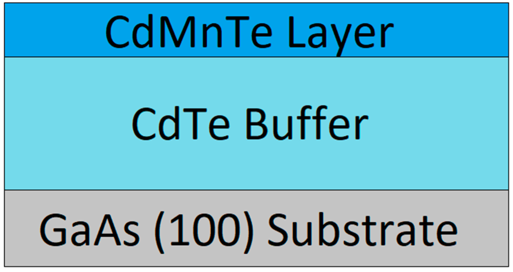
Figure 2.
X-ray diffraction 2θ-ω for all Structures.
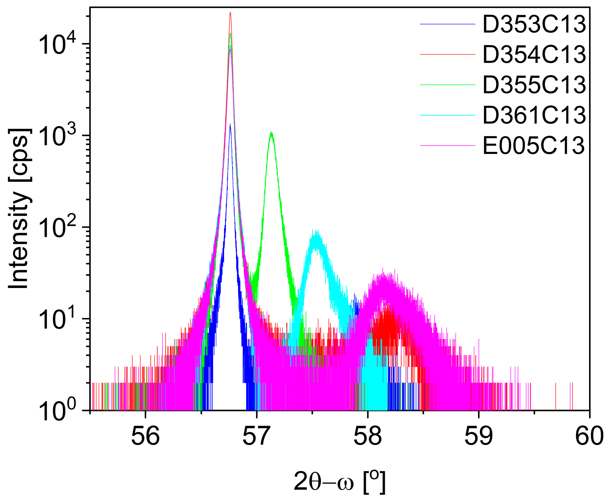
Figure 3.
The reciprocal space map obtained by using symmetric 422 reflection for Structures 1 to 5, a) to e).
Figure 3.
The reciprocal space map obtained by using symmetric 422 reflection for Structures 1 to 5, a) to e).

Figure 4.
The reciprocal space map obtained by using asymmetric 115 reflections for Structures 1 to 5, a) to e).
Figure 4.
The reciprocal space map obtained by using asymmetric 115 reflections for Structures 1 to 5, a) to e).
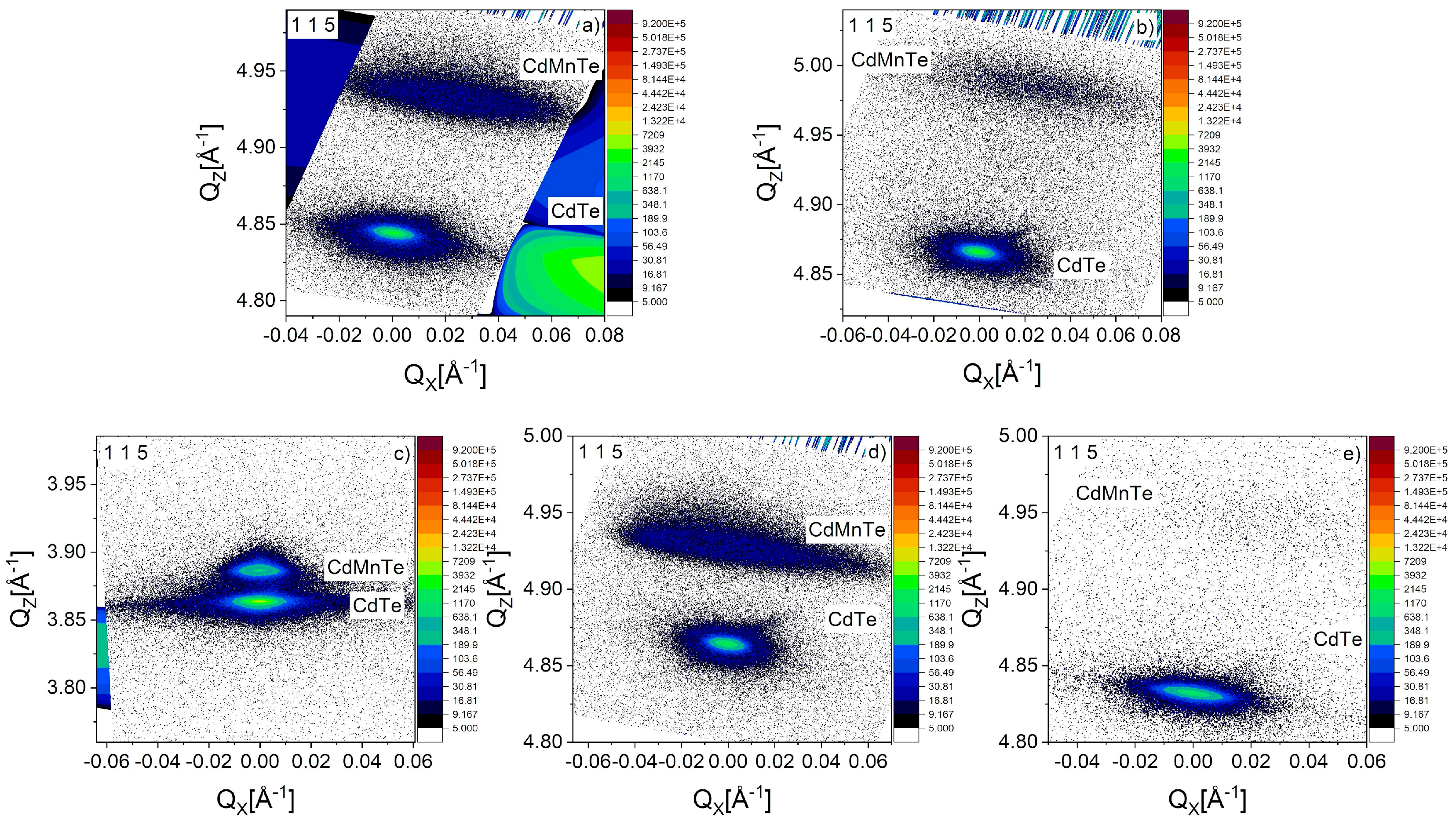
Figure 5.
Nomarski optical micrographs of the surface morphology of CdMnTe films for the Structures 1 to 5, a) to e).
Figure 5.
Nomarski optical micrographs of the surface morphology of CdMnTe films for the Structures 1 to 5, a) to e).
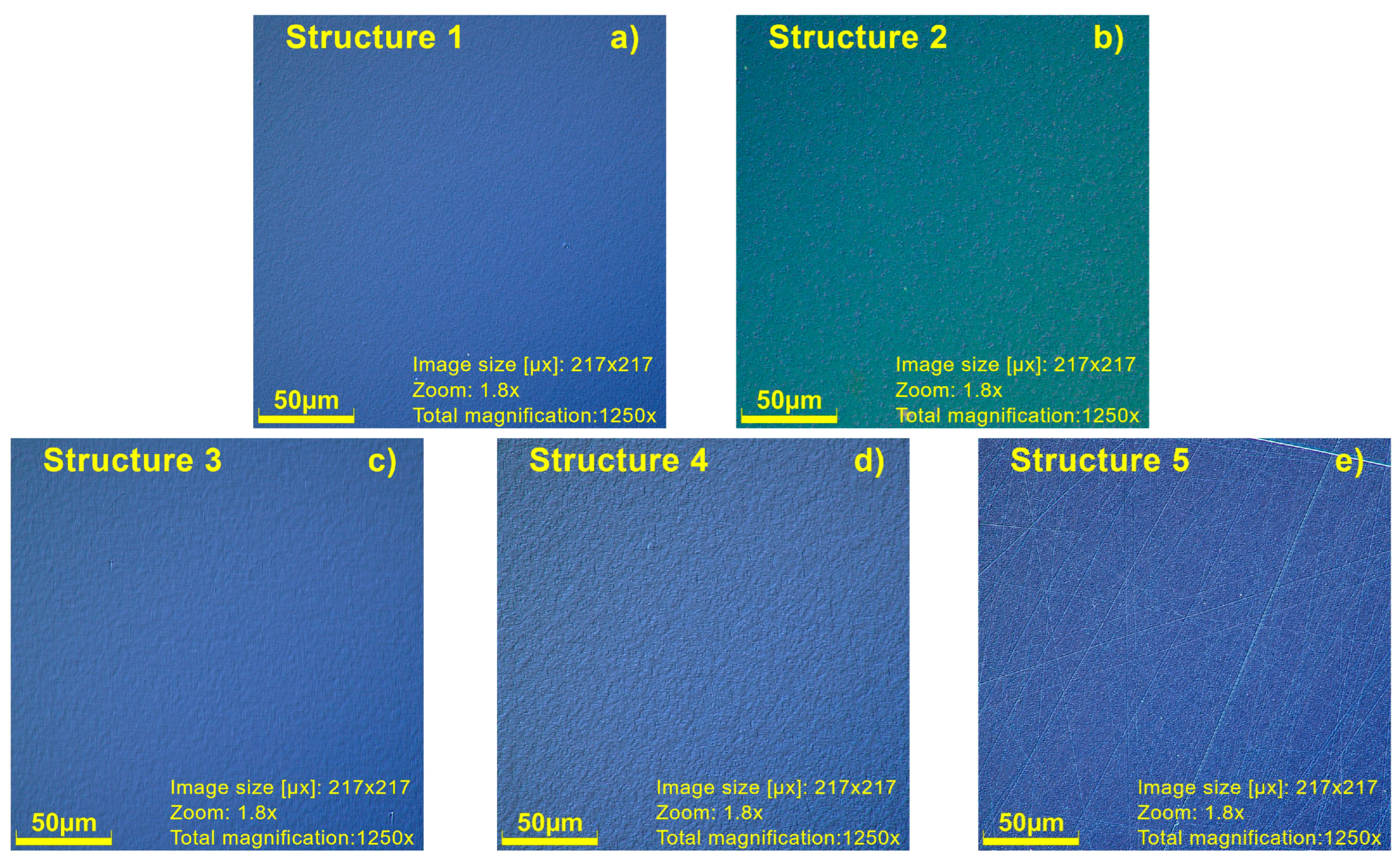
Figure 6.
AFM image of the surface morphology of CdMnTe films for all investigated structures respectively.
Figure 6.
AFM image of the surface morphology of CdMnTe films for all investigated structures respectively.
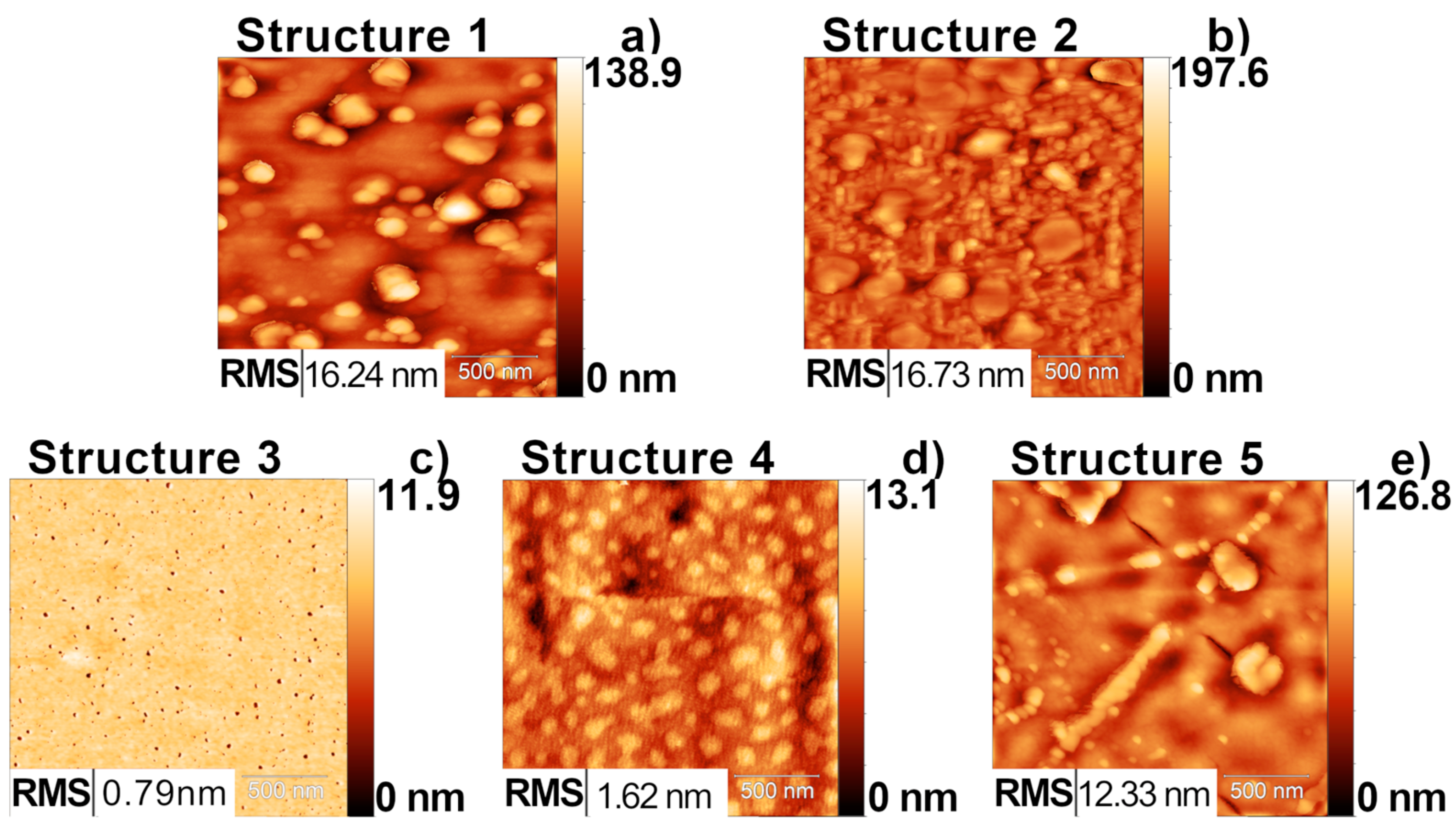
Figure 7.
EPR spectra of manganese in Cd1-xMnxTe with x = 0.073.
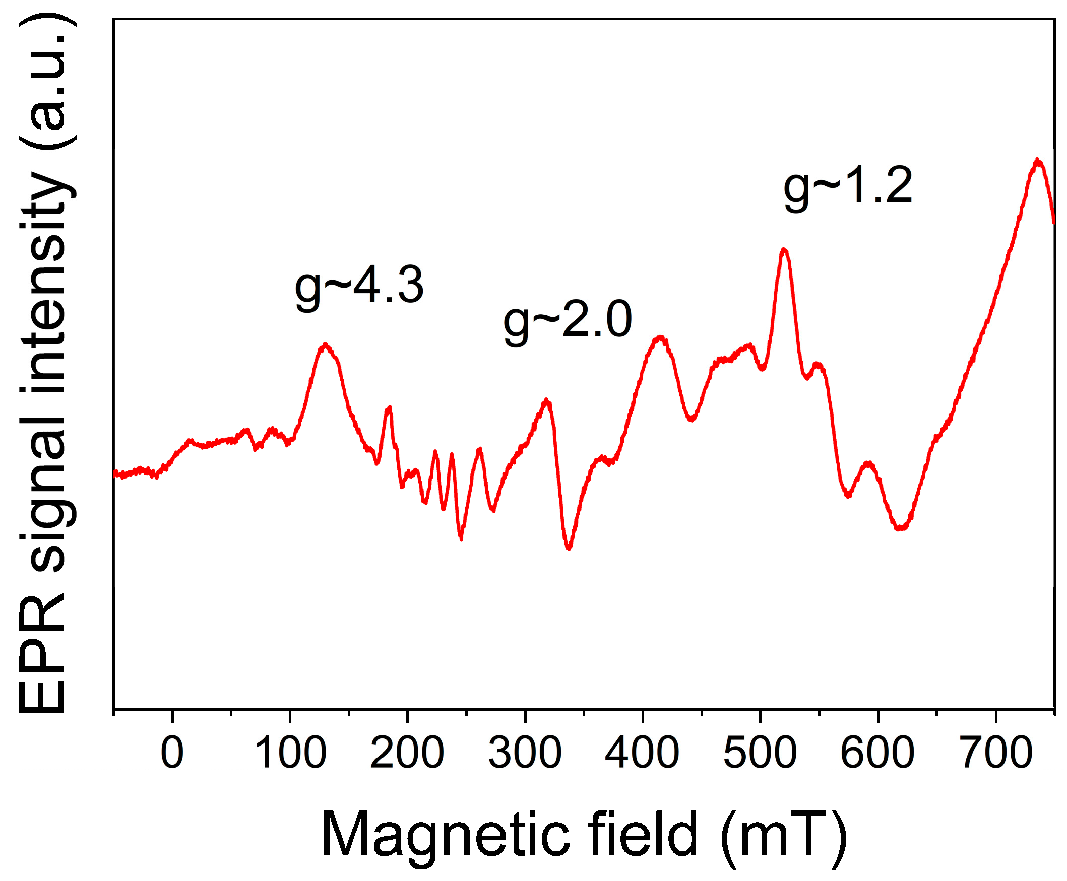
Figure 8.
Temperature dependence of EPR spectra of Cd1-xMnxTe for Structures 1 to 5, a) to e).
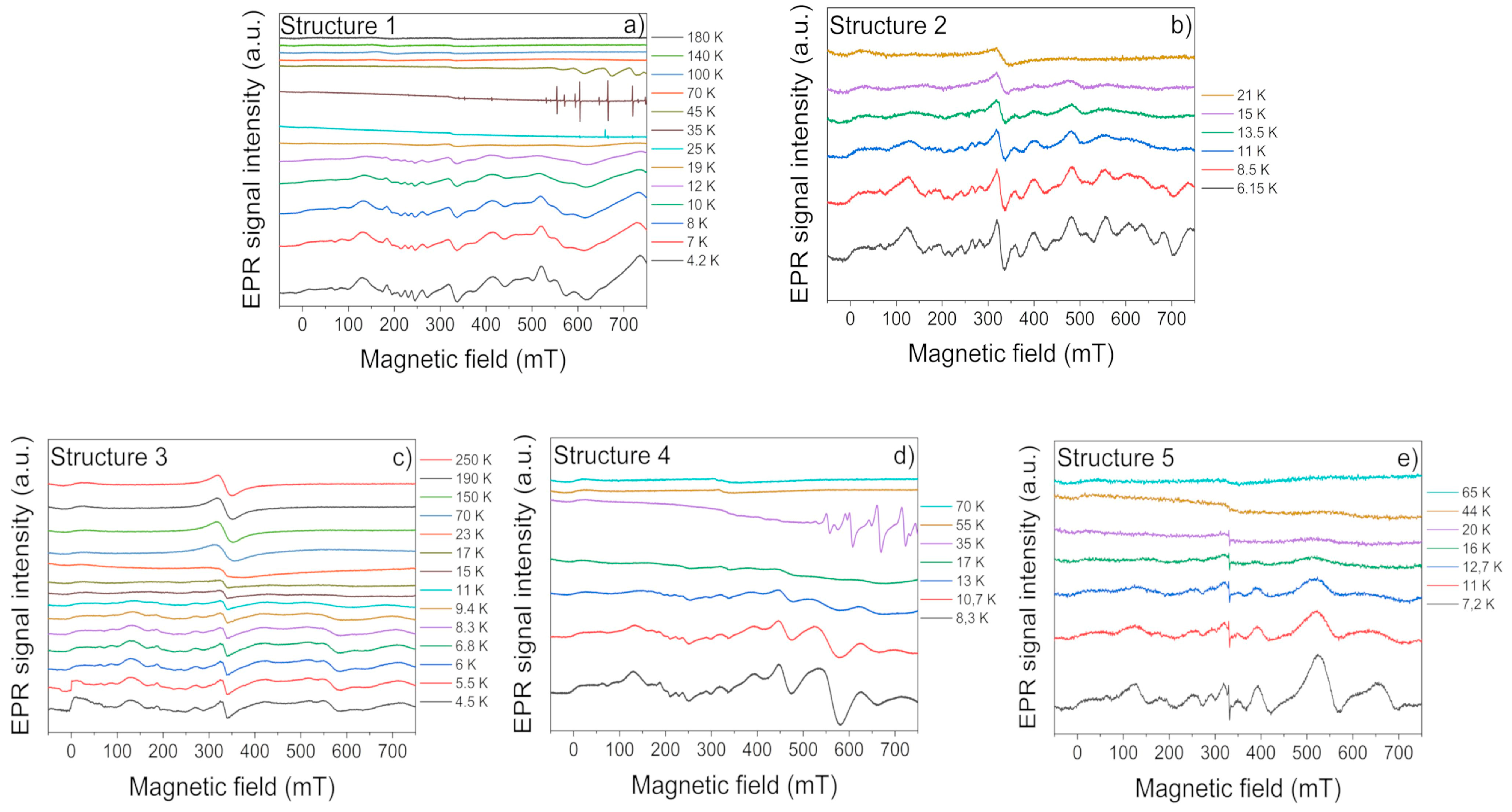
Figure 9.
Inverse of integral intensity versus temperature for Cd1-xMnxTe structures of various Mn x values.
Figure 9.
Inverse of integral intensity versus temperature for Cd1-xMnxTe structures of various Mn x values.
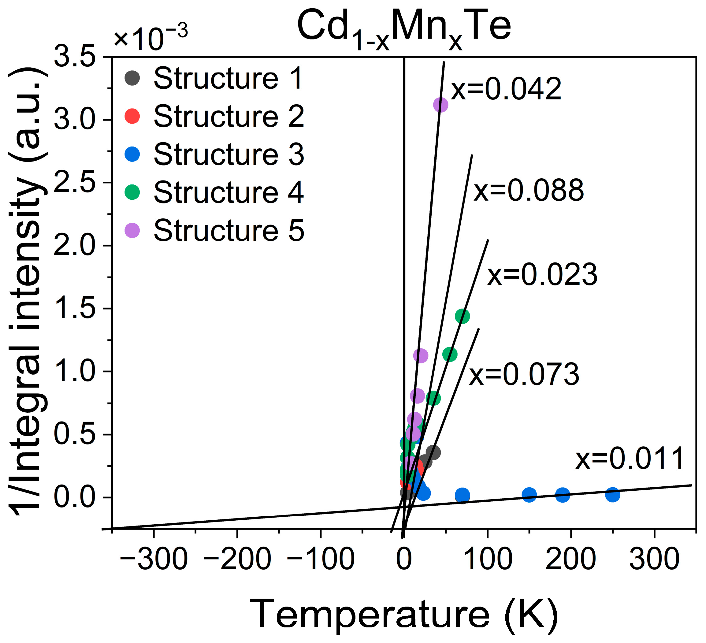
Figure 10.
Curie-Weiss constant for Cd1-xMnxTe structures of various Mn x values.
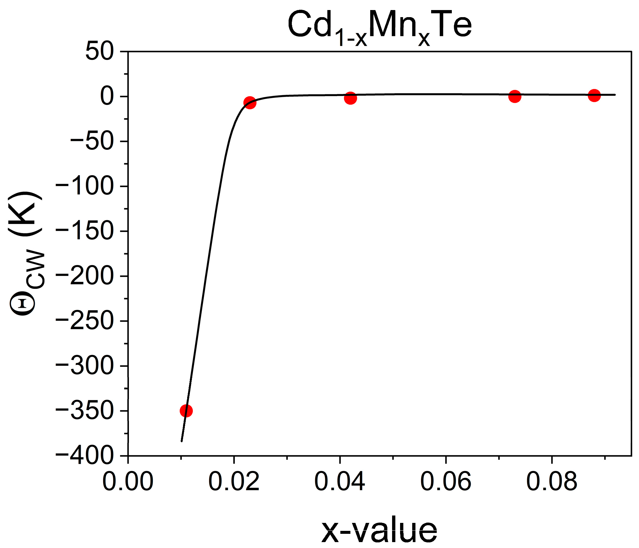
Figure 11.
Effective g-factor for Cd1-xMnxTe structures of various Mn x values.
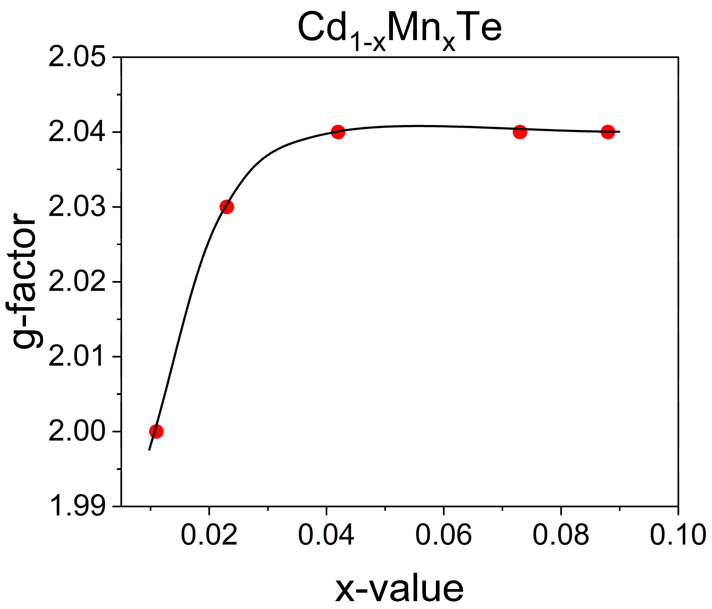

Table 1.
Quantitative comparison of epitaxially grown Cd1-xMnxTe on GaAs (100) substrates.
| Structure name | Epilayer x-value |
Thickness of epilayer SEM (μm) |
Lattice mismatch (ppm) |
Dislocation density (cm-2)×105 |
Mosaicity (×10-6) |
|---|---|---|---|---|---|
| Structure 1 (D353C13) | 0.073 | 0.43 | -17883 | 2.69 | 9.20 |
| Structure 2 (D354C13) | 0.088 | 0.41 | -24028 | 4.51 | 1.88 |
| Structure 3 (D355C13) | 0.011 | 0.40 | -5870 | 1.12 | 13.33 |
| Structure 4 (D361C13) | 0.023 | 0.42 | -1246 | 2.63 | 66.47 |
| Structure 5 (E005C13) | 0.042 | 0.61 | -2184 | 4.79 | --- |
Table 2.
The EPR parameters and Curie-Weiss constant of Cd1-xMnxTe structures (line in magnetic field ≈330 mT).
Table 2.
The EPR parameters and Curie-Weiss constant of Cd1-xMnxTe structures (line in magnetic field ≈330 mT).
| Structure name |
Effective g-factor |
Bpp (mT) | θCW (K) | C (×104) |
|---|---|---|---|---|
| Structure 1 (D353C13) | 2.04 | 28.30 | 0 | 10 |
| Structure 2 (D354C13) | 2.04 | 22.21 | 1 | 5 |
| Structure 3 (D355C13) | 2.00 | 27.56 | -350 | 5000 |
| Structure 4 (D361C13) | 2.03 | 25.98 | -7 | 12.5 |
| Structure 5 (E005C13) | 2.04 | 17.30 | -2 | 5 |
Disclaimer/Publisher’s Note: The statements, opinions and data contained in all publications are solely those of the individual author(s) and contributor(s) and not of MDPI and/or the editor(s). MDPI and/or the editor(s) disclaim responsibility for any injury to people or property resulting from any ideas, methods, instructions or products referred to in the content. |
© 2024 by the authors. Licensee MDPI, Basel, Switzerland. This article is an open access article distributed under the terms and conditions of the Creative Commons Attribution (CC BY) license (http://creativecommons.org/licenses/by/4.0/).
Copyright: This open access article is published under a Creative Commons CC BY 4.0 license, which permit the free download, distribution, and reuse, provided that the author and preprint are cited in any reuse.


