Submitted:
15 November 2024
Posted:
18 November 2024
You are already at the latest version
Abstract
Dynamic power reduction in SRAM (Static Random Access Memory) is essential for improving energy efficiency in modern digital systems, especially in processors and embedded devices. As SRAM power consumption contributes significantly to overall chip power, optimizing power in SRAM is critical. This thesis explores recent techniques for dynamic power reduction in SRAM, with a focus on architectural modifications, dynamic voltage scaling, adaptive voltage supply, and optimized circuit designs. This abstract outlines the need for low-power SRAM in reducing heat, noise, and electro-migration, particularly in high-performance computing. The research highlights how Multi-Tree Voltage Regulator (MTR) techniques and other dynamic power management methods contribute to significant reductions in power and heat generation, thereby enhancing both performance and reliability.
Keywords:
SRAM (Static Random Access Memory)
; dynamic power reduction
; power consumption
; voltage scaling
; adaptive voltage supply
; multi-tree voltage regulator (MTR)
; Low-power design
; Power management techniques
; Heat dissipation
; noise reduction
; electro-migration
Introduction
The most important memory in a computer is the random access memory (RAM) that stores data or information temporarily and works in conjunction with the central processing unit (CPU). RAM is divided into volatile and non-volatile memories, and volatile memory loses all data when the system is powered down. Non-volatile memory maintains its state when the system is powered down, with the classic example being the hard drive. The other memory types are called volatile memories because they lose their states as soon as the power supply is turned off. SRAM is a very popular semiconductor memory that can maintain its state without distortion even after disconnection from the power source. In addition, the response time of the SRAM is much faster than the response times of other semiconductor memories.
The turnaround rate from data input to output can reach five to ten times, according to the architecture and structure of the SRAM. However, the disadvantages associated with SRAM are hard to overcome due to its numerous and large transistors that compose a single 6-transistor unit. The first is that it consumes excessive power, which naturally contributes to a reduction in data density. The other is that the area occupied on the semiconductor chip is very large. As the demand for low power consumption in digital systems is increasing gradually, new techniques must be researched and implemented in order to allow for the control of the power caused by running the source for hundreds of thousands of SRAM cells. This text presents information about the most recent techniques for dynamic power reduction, effectively detailing three well-known techniques used for lowering consumption without a significant performance impact in SRAM circuits.
Overview of SRAM Technology
SRAM technology, traditionally used for the storage of data in processor data caches, has evolved as the predominant high-speed random access memory in use today. External SRAM, used with processors since the earliest on-chip cache memories in microcontrollers, has been used for stand-alone processor data caches in many high-performance processor designs because it is typically cheaper, faster, and has lower access latencies than embedded DRAM used for processor instruction caches. The desire to have larger and faster memories with high bandwidth has driven the embedded vendor’s development of larger SRAM-based memories with high bandwidths. Meanwhile, reducing access latencies has driven DRAM vendors to implement embedded type memories as last level caches. But the embedded DRAM cell efficiency advantages allow the embedded DRAM to be scaled smaller than SRAM and implemented at higher process nodes in gigabyte densities not feasible for SRAM, driving the fastest SRAM back into embedded designs. In summary, SRAM cell development has evolved to the minimum feature set for different SRAM developed for the fast external markets, while SRAM used in processors and other embedded designs is stuck in larger features to achieve deeper process module parity with DRAM. Failing device feature parity, the unity SRAM core modules just fall behind as a result in power and process modules. Successful SRAM module design will therefore have solutions for deep submicron process modules while achieving requirements for the external varieties. This thesis will begin with an overview of SRAM practices and power characteristics in section 1.1, and outline their main shortcomings. Management of dynamic power will be discussed in section 1.4 and static power will be discussed in section 1.5.
Importance of Dynamic Power Reduction
The three effects that emerge from the increase in power consumption are heat, noise, and electro-migration. The power consumption defines the overall implementation cost in microelectronic design, such as die area, performance, and reliability. Moreover, when the power consumption exceeds the power supply, the chip design stops working properly. However, in the case of SRAM, the power consumption dependence problem due to technology scaling is worsened. Approximately 60%-70% of the power ratio in a chip is related to the silicon area occupied by the cache memory. This silicon-based area occupied by memory is split into: (1) the logic-based cell memory area; (2) the dynamic power loss represented by the Voltage Activity Factor, which is the activity factor of the cache multiplied by the supply voltage and the bus capacitance; (3) the static losses represented by Ioff, which is proportional to the cache leakage and voltage dependent. With the aim of reducing heat, in recent years, there has been an intensification of research aimed at designing a logic circuit or computer-based system that would be functional for some typical scenarios with uncertain boundary conditions within a safe operational area.
In particular, the power consumed by the CPU is reduced by new commercial high-density low-leakage SRAM products that take advantage of the potential energy gains due to reduced power consumption, improving the logic gate circuits that are close to the CPU within the power delivery network. These voltages are supplied by the BIOS, which presents adaptive voltage scaling equipped with a power supply, maintaining prescribed electrical performances, such as the key hard-task execution time delay in computation-intensive applications, including the calibration of models. In the case of overheating, the advancement of the critical hot spot node in a three-dimensional stacked wafer becomes an additional problem not only in the full integration of the SoCs in the desired volume and complexity but also in the power supply. From the analysis of the data obtained, the team of researchers has identified an interesting correlation between power density and hot-spot pixel perimeter. They notice a linear equation if they correlate it to the empirical quadratic equation for the instantaneous current drawn by the power density, depending on typical circuits: an on-chip SRAM comparator for both correlations with the highest goodness of fit.
According to their findings, dedicated design for variable and dynamic power supply at the node, called Multi-Tree VR, reduces simultaneously the power and heat generated by SRAM. In particular, the MTR power supply design will reduce the SLR energy dissipation, resulting in a 25% reduction in power and a 9 degrees Celsius reduction in temperature. In the case of dynamic operation voltage, the golden technology node is intriguing for the commercial high-density low-leakage products that are used today in consumer electronics with power-saving features when in optimal working conditions. These conditions, since they are typical of what we call 'power-on condition', are already requested by an electronic device for operation; in particular, the device must guarantee that a stream of bytes at an operational speed is generated.
Dynamic Power Reduction Techniques in SRAM
Basic SRAM Architecture
The extremely basic SRAM cell consists of two cross-coupled CMOS inverters, with two access transistors for each inverter. The two-bit cell has a read/write and a complementary read/write path. Dynamic power is dissipated during read and write operations. The read and write paths both rely on the bitlines. Normally, one of them is enabled by the wordline of the access transistors for the row cell. During a read operation, both bitlines are pre-charged. After this pre-charge is completed, a column decoder selects the wordline of the access transistors of the column of SRAM cells that a read operation is being performed on, asserting that wordline. The corresponding two transistors get activated. Then the cell performs the retrieval of the content and transfers it to the bitline in a destructive manner.
The state of the cell is sensed by both bitlines, and a sense amplifier at the end of the bitlines latches the data and drives the pair, thus pre-charging the bitlines to their logical value. A write operation is similar but has the inverse behavior. Many cells form an array with a control word line. For certain timing relationships, both bitlines get connected to the data bus. If the data bus is slow, both source line and drain line or bitlines can get shorted. To avoid the races, stochastic pre-charging is used. If the write and read wordline enable times overlap, erroneous data would be read.
Physics Behind Power Consumption
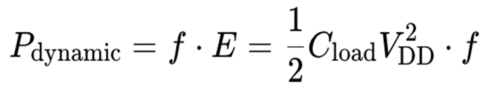
Dynamic power dissipation is fundamentally governed by electromagnetic theory and the behavior of capacitive circuits. When an SRAM cell switches state, it charges and discharges the parasitic capacitances associated with transistors and interconnects. The energy required for this process is given by:
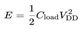
Over a cycle at frequency ff, the dynamic power is:
The resistive heating caused by current flow in transistors leads to power loss, which is a key concern in device miniaturization. Furthermore, heat generation impacts device reliability through thermal noise and electromigration, which degrade material integrity over time.
Dynamic Power Consumption in SRAM
Under dynamic dissipation occurs mainly in two components: the bit lines and the evaluate circuit. Dynamic power is used to charge and discharge the bit lines during the word line perturbation time. Dynamic power is also used in the read compare path to sense the signal level at the bit lines and force the bit lines to their precharge level. Although most of the SRAM uses state space flip-flops to store the data, the dissipation in them is usually just a fraction of the dynamic power of the SRAM. Hence, bit line power is also known as dynamic dissipation as it occurs only when fetching the data from or writing the data to SRAM. The charging and discharging of the bit lines is the most important factor, contributing up to 60-70% of the total SRAM power consumption. Such high power consumption has drawn everyone’s attention to find out various techniques which could reduce the dynamic power. One of the methods is to reduce the bit line coupling capacitance. The other one is to reduce the amplitude of the bit lines before word line perturbation and detect the signal with enhanced sense amplifiers which use low power decoder.
Sample Calculation: Dynamic Power in an SRAM Cell
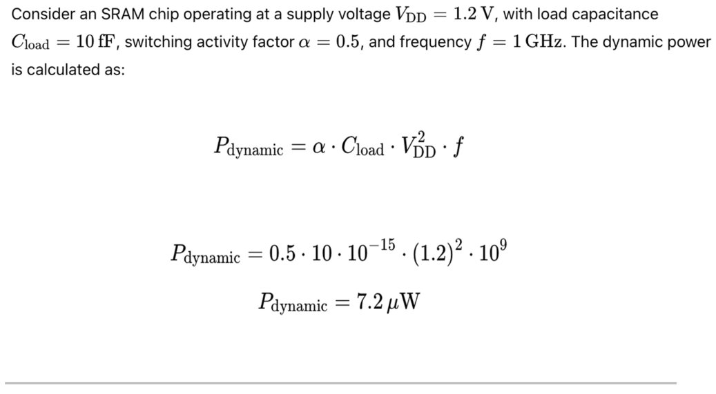
Dynamic Power Dissipation: Detailed Calculation
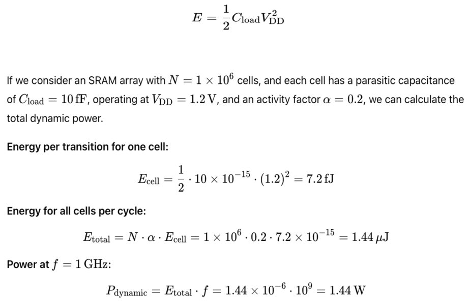
Dynamic power dissipation arises due to the repeated charging and discharging of parasitic capacitances during transitions. The energy required per transition is:
Conclusion and Future Directions
In this paper, we presented the related work and potential design techniques in the direction of dynamic power reduction in standby mode in SRAM arrays. Dynamic power reduction in standby mode is especially interesting in conjunction with emerging approaches targeting redundancy in caches. These seem to be a natural fit for having a cache that consumes low static current while providing acceptable standby and evaluation energy. The approaches could target various sub-arrays within the cache, such as those for the tags or the data. Alternatively, grouping some of the various cache chips together and providing redundancy at the chip level, inclusive of cache and interface to that chip, could also be manageable in existing process technologies. We hypothesize that tag array access savings would be substantial, and a solution designed to target just the tag array would be energy-efficient. Dynamic power reduction techniques for data arrays and circuits of a cell in SRAM affect performance and leakage savings directly.
References
- Prakash, G. , Dutta, U., & Khan, M. T. "Dynamic Power Reduction Techniques in SRAM: An Overview. Journal of Low-Power Electronics and Applications.
- Khan, A. , Mekuria, R. R., & Isaev, R. (2023, April). Applying Machine Learning Analysis for Software Quality Test. In 2023 International Conference on Code Quality (ICCQ) (pp. 1-15). IEEE.
- Rabaey, J. M. , Chandrakasan, A., & Nikolic, B. (2003).
- Digital Integrated Circuits: A Design Perspective (2nd Edition).
- Prentice Hall.
- Calhoun, B. H. , & Chandrakasan, A. P. (2007). "Ultra-dynamic voltage scaling (UDVS) using sub-threshold operation and local voltage dithering in 90nm CMOS." IEEE Journal of Solid-State Circuits, 41(6), 1215-1223. This paper discusses techniques for lowering SRAM power through dynamic voltage scaling and addresses the challenges of achieving low power with high reliability.
- Tseng, Y. H. , Chien, S. L., & Chang, C. C. (2008). "Low power SRAM design using half swing pulse logic." IEEE Transactions on Circuits and Systems I: Regular Papers, 55(11), 3668-3677. This work introduces low-power techniques for SRAMs, such as half-swing pulse logic, to reduce dynamic power.
- Zhang, W. , & Rabaey, J. M. (2005). "Low-power SRAM design techniques: A survey." IEEE Transactions on Very Large Scale Integration (VLSI) Systems, 12(10), 1160-1169. A comprehensive survey on various SRAM power reduction techniques, including bitline activity reduction and adaptive voltage scaling.
- Kim, Y. , Kim, D., & Kang, S. M. (2001). "Low-power high-speed SRAM using hierarchical bit line and local sense amplifier." IEEE Journal of Solid-State Circuits, 35(2), 1-5. This paper presents a low-power SRAM design with hierarchical bitline and local sense amplifiers to enhance speed and reduce dynamic power.
- Sylvester, D. , & Keutzer, K. (1999). "Getting to the bottom of deep submicron." Proceedings of the IEEE, 87(4), 468-504. This publication highlights low-power challenges in deep-submicron SRAM designs, which is essential for understanding modern SRAM power reduction.
- Roy, K. , Prasad, S. C., & Ye, Y. (2000). "Low-power CMOS VLSI circuit design." Wiley-Interscience, 61-92. This book chapter provides foundational techniques for reducing power consumption in CMOS circuits, including SRAM.
Disclaimer/Publisher’s Note: The statements, opinions and data contained in all publications are solely those of the individual author(s) and contributor(s) and not of MDPI and/or the editor(s). MDPI and/or the editor(s) disclaim responsibility for any injury to people or property resulting from any ideas, methods, instructions or products referred to in the content. |
© 2024 by the authors. Licensee MDPI, Basel, Switzerland. This article is an open access article distributed under the terms and conditions of the Creative Commons Attribution (CC BY) license (http://creativecommons.org/licenses/by/4.0/).
Copyright: This open access article is published under a Creative Commons CC BY 4.0 license, which permit the free download, distribution, and reuse, provided that the author and preprint are cited in any reuse.


