
Submitted:
13 November 2024
Posted:
14 November 2024
You are already at the latest version
Abstract
Single molecule fluorescence spectroscopy offers unique capabilities of low concentration sensing or probing molecular dynamics. However, employment of such methodology for versatile sensing and diagnostics under point-of-care demands device miniaturization down to lab-on-a-chip sizes. Here, we numerically design metalenses with high NA of 1.1 that are composed of silicon nitride nanostructures deposited on a waveguide and may selectively focus guided light into an aqueous solution at two wavelengths of interest in a spectral range between 500 and 780 nm. Despite the chromatic focal shift in lateral directions owing to the wavelength-dependent propagation constant in a waveguide, a segmented metalens provides perfectly overlapped focal volumes which meets the requirements for epi-fluorescence light collection. We demonstrate that the molecule detection efficiencies for metalenses designed for excitation and emission wavelengths of fluorophores ATTO 490LS, Alexa 555, APC-Cy7 tandem are sufficient to collect several thousand of photons per second per molecule at modest excitation rate constants. Such sensitivity provides a reliable diffusion fluorescence correlation spectroscopy analysis of single molecules on chip to ex-tract their concentration and diffusion properties in the nanomolar range. Altogether, an achromatic integrated metalens opens new avenues for development of ultracompact and sensitive devices for precision medicine and environmental monitoring.
Keywords:
Achromatic metalens
; biosensors
; photonic integrated circuits
; waveguide
; fluorescence correlation spectroscopy
; single molecules sensing
1. Introduction
Single molecule fluorescence is of paramount importance for investigation of molecular biophysics process hidden from ensemble measurements [1]. Extreme sensitivity and access to temporal dynamics monitoring make it an appealing methodology for sensing of biomolecules and nanoparticles and diagnostics [2,3,4]. Nevertheless, optical single molecule sensing platforms require bulky and costly elements that hinder sensing and diagnostics outside a laboratory. Several miniaturized single molecules platforms have been shown based on 3D printed microscopes or nanoantenna systems with smartphones [5,6]. However, integrating of single molecule sensing units with photonics integrated circuits would result in ultimate sensor miniaturization and portability [7]. The development of optical components has undergone a transformative shift with the advent of metasurfaces [8,9,10], leading to the rise of metalenses—flat, ultra-thin lenses that manipulate light through engineered nanostructures. Unlike refractive lenses that rely on curved surfaces to refract light, metalenses modulate phase at a designed manner to result in a desired output field. Metasurfaces modulating output light phase at will represent compact optical devices for imaging, holography, spectrometry and more [11,12,13]. Thanks to the abundance of low-loss high-refractive index materials metalenses can be designed in a broad range of wavelengths from ultraviolet and visible [14,15,16] to infrared and terahertz frequencies [17,18]. This versatility opens up new possibilities for miniaturized optical systems in various applications ranging from telecommunications to biomedical imaging and sensing [19,20,21]. Low footprint and complementary metal-oxide semiconductor compatibility make them appealing for creating on-chip optical devices via integration into photonic circuits to manipulate light propagation in the free space. To control the scattering of light off-chip the meta-atom modes can be coupled to a guided photonic waveguide inducing modulation of phase and intensity [22,23]. That enables controlled light emission into free space, such as out-of-plane beam deflection, focusing, and holographic projection [24,25,26,27,28]. This optical device integration unlocks diverse practical applications for data storage, 3D display, and quantum computing [28,29,30].
Regardless of the rising interest in integrated metasurface photonics, studies of on-chip metasurface for fluorescence sensing applications have remained scarce. In order to yield single molecule sensitivity under epi-fluorescence conditions with state-of-the art detectors, one requires a high numerical aperture lens with well-overlapped excitation and detection volumes for the wavelengths of interest [31]. Free-space metalenses can focus light without chromatic aberrations via phase profile compensation at multiple wavelengths [32,33]. Multi-layer stacked transmissive metalenses unlock additional degrees of freedom for control of phase and amplitude and produce multi-wavelength focusing [16,34]. However, multilayer structures on chip would require incredibly delicate nanofabrication processes. The segmentation of the metalens zones represents an efficient way of making multifocal or achromatic transmissive metalenses via modulation of focusing properties of each selected zone [35,36,37]. Recently, single molecule fluorescence detection has been experimentally shown with a free-space transmissive metalens [38]. Unlike transmissive lens optics, the chromatic focal shift produced by an integrated metalens occurs in both axial and lateral dimensions making the focal volume overlap challenging to achieve. In this work, we demonstrate first, to the best of our knowledge, numerical designs of dual-wavelength metalenses on a planar waveguide of high numerical aperture (NA=1.1) that provide perfect focal volume overlap for sets of two separated wavelengths in a large spectral range in the visible and IR. The metalens is composed of cylindrical silicon nitride nanoposts on top of a silicon nitride planar waveguide, and segmented into even rectangular zones that are designated to vertical focusing one of the two wavelengths at a defined focal length. High NA metalens provides sufficiently tight focusing to efficiently excite single point emitters and collect light from them at design wavelengths. By selecting metalens design wavelengths according to favorable excitation and emission wavelengths of three model fluorophores ATTO 490LS, Alexa555, APC-Cy7, we determine the molecule detection efficiencies around the focal volume under epi-fluorescence excitation. Given the sufficient number of collected photons, we simulate fluorescence correlation spectroscopy (FCS) data of molecules diffusing through the metalens detection volume. The possibility of running FCS represents a unique platform for single molecule fluorescence monitoring on chip. Altogether, the epi-fluorescence achromatic metalenses on waveguide pave the way for devices with ultimate miniaturization and sensitivity for portable diagnostics settings and precision medicine.
2. Materials and Methods
Numerical simulations of optical performance of the metalens on waveguide were performed via finite difference time domain (FDTD) method. The planar waveguide and meta-atoms are composed of silicon nitride [39]. We select silicon nitride as a material for the waveguide and meta-atoms as this material exhibits low losses compatible with visible photonic integrated circuitry and rather elevated refractive index for effective light coupling. The metalens of 20 µm size is placed on a tapered waveguide. The point spread functions (PSF) are acquired for three metalens designs which provided achromatic focusing at NA=1.1 at excitation and emission wavelengths of selected model molecules. The fundamental mode TE0 is injected into the waveguide. The simulation region boundary conditions are set to perfectly matched layers (PML). The maximum collection efficiency of the metalens is estimated via placing an isotropic source into the focal volume of the metalens and monitoring the fraction of power collected inside the single mode waveguide. The model fluorescent molecules are ATTO 490LS, Alexa Fluor 555, APC-Cy7 that absorb light in the visible and infrared light. The molecule property data are retrieved from https://www.aatbio.com/. The fluorescent label ATTO 490LS has a large Stokes shift of 165 nm, with a maximum absorption peak at 496 nm and a maximum fluorescence peak at 661 nm. APC (Allophycocyanin)-Cy7 is a fluorescent compound with an excitation peak at 651 nm and an emission peak at 779 nm. Alexa Fluor 555 is a fluorescent compound with excitation peaks at 520 and 553 nm, while its emission peak locates at 568 nm. Fluorescence correlation spectroscopy data are simulated via Monte-Carlo simulations (SimFCS3 https://www.lfd.uci.edu/globals/) with 300 molecules diffusing inside a box of 2.4×2.4×2.4 µm3 that is constituent of cubic unit cells of 50 nm. The molecules stochastically move from one unit cell to another resembling isotropic 3D diffusion. The autocorrelation functions are reconstructed based on the single molecule brightness and diffusing time.
3. Results
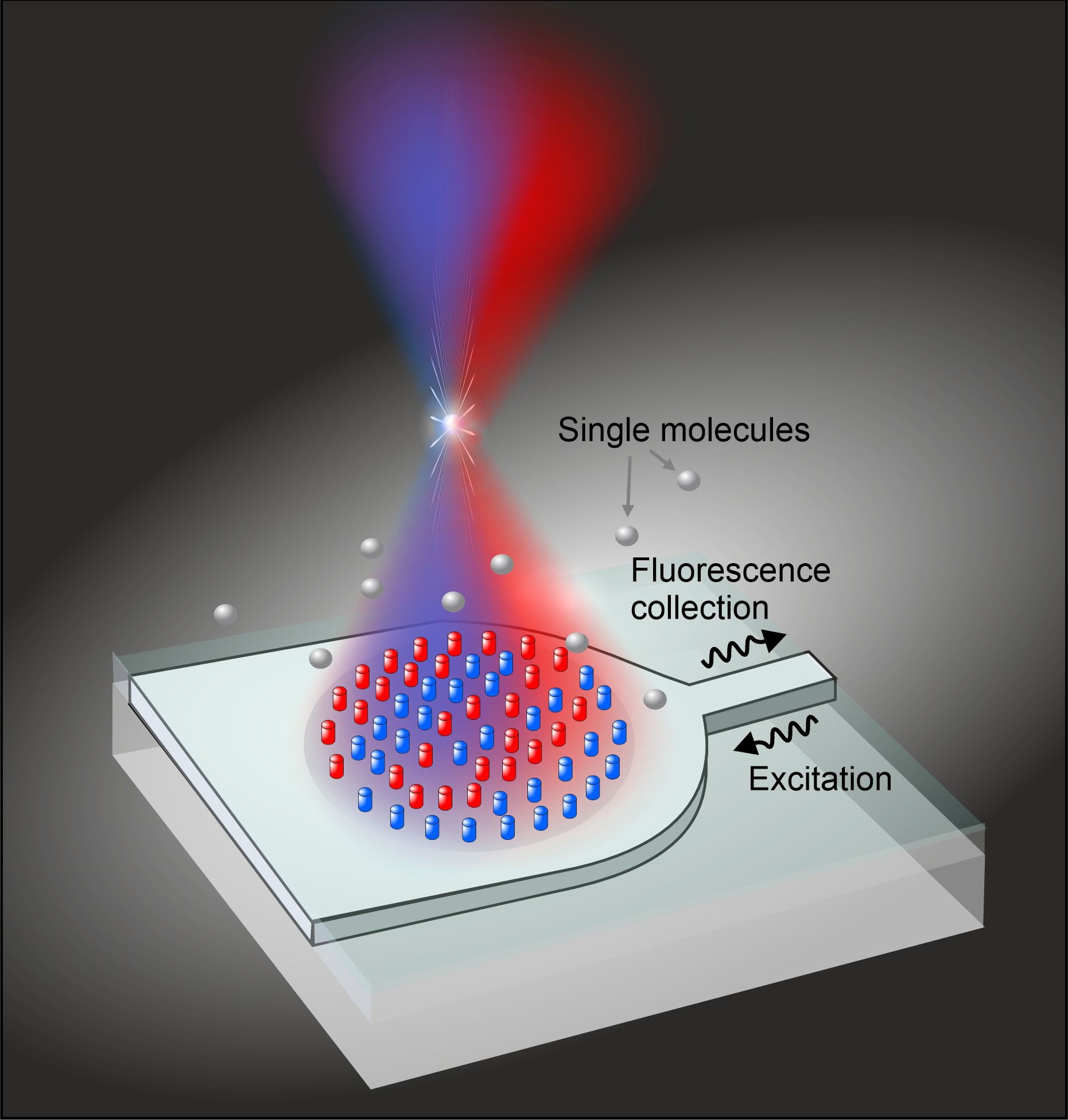
Figure 1 represents the design concept and operation of the dual-wavelength metalenses on a planar waveguide for single molecule sensing. The light of the excitation wavelengths is focused by the metalens inside water medium with a high NA to provide an efficient excitation of freely diffusing molecules and large collection efficiency (Figure 1 a). However, in order to support substantial fluorescence collection, the emission light around the maximum of fluorophores has to be collected exactly from the excitation focal volume [31,38]. To provide the detection only from the focal volume we add a cladding layer of silica-on-glass (SOG) layer of a few µm thick to prevent evanescent waves of the guided mode reach the water medium. We segment a metalens into equal alternating rectangular zones of two types, where one type is designed to produce a focal volume at the excitation wavelength (λ1), and the other type generates a focal volume at the same place at substantially different emission wavelength (λ2). In order to mimic the phase pattern of the outcoupled light in the free space we assess phase accumulation inside the waveguide. We numerically simulate a periodic diffraction grating of cylinder nanoposts on top of a waveguide. By monitoring the diffraction angle in the far field, we could deduce the propagation constant (β) according to the following relation: with n being the refractive index of the top cladding, θ the angle of the outcoupled radiation, Λ is the grating period. By setting Λ at 365 nm, the grating supports close to vertical light propagation at a large frequency band in the visible. Then, we set the meta-atoms in the intersection positions of the waveguide accumulating phase () and the lens phase equation (). Moreover, to correct the curved wavefront in the taper we compensate the input phase passing by first meta-atoms. Thus, the meta-atom positions (x,y) satisfy the condition (Figure 1 b). These two functions can be expressed as follows:
Here, equals 0 for y values outside the i-th segment and 1 for y values inside the i-th segment (Figure 1 c), F is the focal distance of the metalens on waveguide in the cladding medium.
We select F according to the design numerical aperture as: . The focal distance for such a metalens size exceeds ten wavelengths for selected excitation wavelengths making it a purely far-field-based detection system. Equation (1) for is valid as long as the coupling strength between a meta-atom and waveguide remains weak, so that the coupling strength is significantly lower than the imaginary part of the eigenfrequency of the hybrid cylinder-waveguide mode. Coupling strength defined via coupled modes theory with the integral over the base of the cylinder (being the scattering port) of the fields and of the quasi-normal mode of the cylinder, and fields and of the guided wave [40]. To avoid difficulties of normalization of radiative quasi-normal modes one can consider ratio of coupling strength to (Figure 1 d). Our calculations show that this ratio does not exceed , proving that waveguide and cylinder modes are indeed weakly coupled. The coupling strength rises with the fill factor of the junction area of the meta-atom and waveguide. We fix the meta-atom diameter at 200 nm to provide sufficiently high coupling strength without perturbing the phase accumulation process in the waveguide. Increase of the diameter leads to perturbed focusing into free space and low inter-cylinder distance which would complicate a fabrication process of the device. The near-field transmission is reduced at low meta-atom heights (Figure 1 e), therefore the selected height of 500 nm yields transmission about 90 % in a broad wavelength range.
To consolidate the potential of the methodology for single molecule sensing on chip, we select 3 fluorophores as model analytes with large and modest Stokes shifts: ATTO 490 LS, Alexa Fluor 555, APC-Cy7 tandem molecule. The models are relying on the datasets of the molecule spectrum, quantum yield, and fluorescence lifetime. Thus, three dual-wavelength metalens designs are modeled to efficiently excite the molecules and collect fluorescence around the emission maximum as follows: 500 nm and 660 nm for ATTO 490LS, 520 nm and 570 nm for Alexa 555, and 650 nm and 780 nm for APC-Cy7. The light propagation from the single mode waveguide toward the metalens on top of a taper and coupling to free-space radiation is simulated with FDTD. We retrieve point spread functions (PSF) for three designs at the wavelengths of interest. The dual-wavelength metalenses on chip produce well-defined focal spots in water medium with well overlapped contours along axial and lateral directions (Figure 2 a, c, e). For the sake of comparison, we additionally simulate a one-segment metalens on chip for excitation wavelength only (Figure 2 b, d, f). The focal spots at the emission wavelengths are formed at highly deviated position in both the axial and lateral directions. Although, the axial position shift arising from the wavelength-dependent lens phase profile, the propagation constant difference produces propagation angle change that leads to drastic lateral focal position shift and focal volume distortion. The significant focal volume mismatch makes the epi-fluorescence sensing with a chromatic integrated metalens elusive. In the case of dual-wavelength metalenses, the large wavelength separation enhances nearly completely avoids a second focus residual intensity in the PSF (Figure 2 a, e). However, even for Stokes shifts of 50 nm (Figure 2 c), the residual intensity from the second focus remains minor as the light propagation along the vertical direction from the metalens remains more favorable. The focusing efficiency of the metalens varies from 8 to 10 % for each wavelength which competes well with independent designs of single-wavelength integrated metalenses [41]. Owing to the symmetry of the scattering matrix of the system metalens-waveguide-environment, the dynamics of such a system is reciprocal [42]. Therefore, the problem of the light outcoupling from the waveguide and the incident light collection by the waveguide from free space can be considered equivalent.
In the context of FCS produced with epi-fluorescence configuration, the diffusing molecule emission can be detected only if the excitation and detection focal volumes are overlapped. The metalens focal spots at molecule excitation and emission wavelengths exhibit perfect spatial match in the lateral dimensions, proving that the difference of φwg at two wavelengths is totally compensated for producing focusing with high NA (Figure 3 a, d, g). The beam diameters (FWHMx/y) approach the diffraction limit of conventional high NA objective lenses. The metalenses designed for Alexa 490 LS, Alexa 555, and APC-Cy7 tandem molecule have beam diameters of 220 nm, 250 nm, and 276 nm at corresponding excitation wavelengths (Figure 3 b, e, h). The beam diameters well approach the diffraction limited performance of analogue free-space lenses. Similarly, the axial chromatic shift is corrected for all three designs, whereas the focal distance mismatch is inferior 50 nm (Figure 3 3 c, f, i).
In this case, molecule detection efficiency (MDE) under epi-fluorescence configuration is represented as [43,44]:
with Iexc being the excitation intensity profile and CEF the collection efficiency of emission within a detection frequency band. The molecule dipole rotation processes occur several orders of magnitude faster than the diffusion time through a microscopic focal spot, therefore, diffusing molecules are normally considered as isotropic point sources in the context of 3D diffusion FCS. The collection efficiency of the isotropic diffusion source in the focal volume is expressed as:
with Pmax being the fraction of coupled emitted photons into the waveguide from an isotropic light source located in the focal volume at the emission maximum, Idet point spread functions at the detection band around the emission wavelength, F(λ) denoting fluorescence intensity spectra of the molecules of interest (Figure 4 a, b, c). As the metalens design operates for TE0 modes, only 1/3 of photons emitted by the isotropic source can be collected. The proposed metalens designs yield MDE values of 0.015 to 0.05 % for ATTO 490LS, Alexa 555, APC-Cy7 (Figure 4 d, e, f). Regardless of this low value, it’s worth noting that even objective lenses of high transmission and aberration correction quality often yield MDE between 0.1 and 1 % [45]. In contrast, the miniaturized on-chip metalens has extremely small thickness of 500 nm and lateral size of 20 µm with potential possibility to massively produce them within photonic integrated circuits.
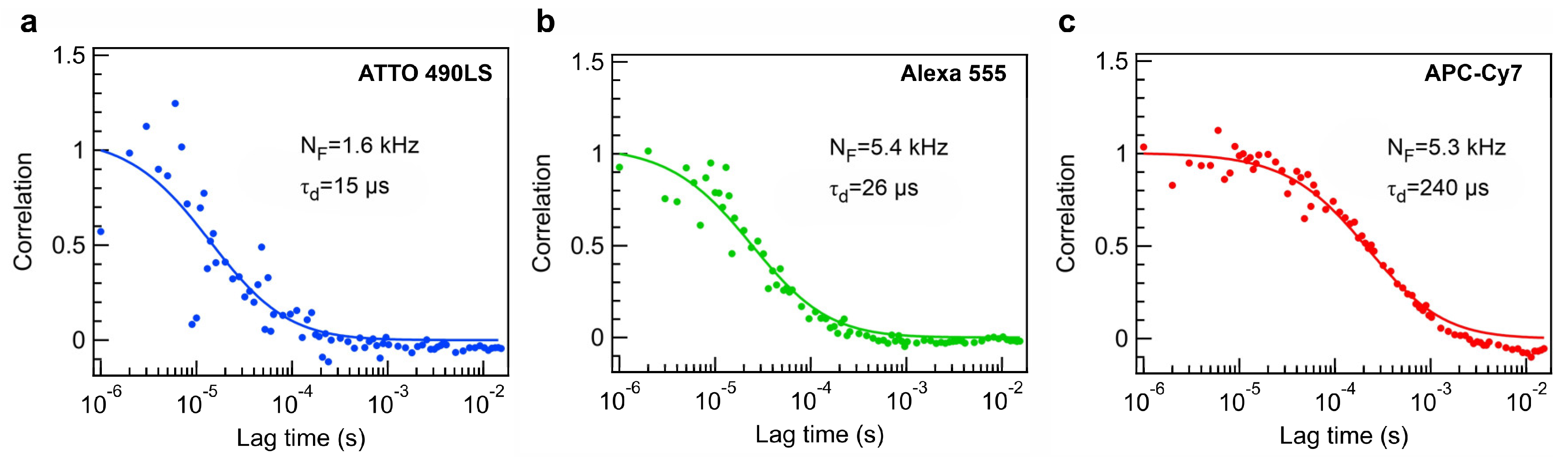
To numerically assess possibility to collect sufficient number of photons from single diffusing molecules, we utilize the formalism of molecule emission based the two-level system with low excitation intensity. The number of collected photons from the molecules in the absence of photobleaching is determined as [46,47], where ψ is the quantum yield of the molecule, denotes time independent average population of the singlet excited state and amounts to with being the fluorescence rate constant and kex the excitation rate constant. By exploiting available datasets of quantum yields, fluorescence spectra, and fluorescence lifetimes () for the molecules of interest we compute number of collected photons per molecule under condition of , which would support negligible photobleaching probability condition in real experimental applications. We estimate that our metalens designs enable single molecule count rate of 1.6 kcounts/s, 5.4 kcounts/s, and 5.3 kcounts/s for ATTO 490LS, Alexa 555, and APC-Cy7 molecule. These single molecule brightness levels exceed the requirements to run diffusion fluorescence correlation spectroscopy, that allow directly probing the number of molecules and their size thanks to the fluorescence intensity fluctuations (Figure 5 a, b, c). The possibility to observe auto-correlation functions within a reasonable acquisition time would serve as robust proof of single molecule sensitivity [48] and a read-out of the biomolecule size and concentration. The acquisition time set in the experiments amounts to 30s which complies with common FCS sensing measurement settings. The fluorescence correlation functions are reconstructed with high signal to noise ratio, while the latter rises with higher NF and MDE as expected from theory. The autocorrelation function noise reduces linearly with increasing NF. Although, in a real experimental conditions other loss channel may lead to reduction of NF they can be partly compensated by kex or accumulation time increase. The detection volume of the metalens in the far field is around 0.17 fl which is applicable to study molecular dynamics at nM concentrations.
4. Discussion
We numerically demonstrated, to the best of our knowledge, first dual-wavelength metalens on a planar waveguide with high numerical aperture. Photonic integrated circuits represent ultimate miniaturization scheme of optical sensing devices [7] making the methodology valuable for truly portable sensors. The proposed metalens design relies on spatial segmentation of the meta-atom regions, where each segment is devoted to produce a vertical focusing of light at one or the other wavelength. The design can be easily tuned depending on the choice of two wavelengths in a broad spectral range. By selecting wavelengths for favorable molecule excitation and collection we model epi-fluorescence sensing of diffusing single molecules ATTO 490 LS, Alexa 555, and APC-Cy7. Owing to extreme focal shift in lateral and axial direction for substantial wavelength separations, the proposed method appears to excite and collect single molecule fluorescence on a chip for molecules with a large Stokes shift. Thanks to the perfect overlap of the focal volumes and high NA of the metalens, the count rate per single molecule reaches a few thousands of photons per second. This sensitivity level is sufficient to run fluorescence correlation spectroscopy analysis to probe the concentration, size and molecular interactions or binding of a labeled biomarker at nanomolar concentrations on a chip. Although, the proposed methodology requires state-of-the-art fabrication facilities and complex optical setups for the experimental concept demonstration, the geometry of silicon nitride nanoposts and a tapered waveguide can be treated with state-of-the-art nanofabrication technologies. Similar to near-field metasurfaces allowing sensitive biomarker detection, the far-field on-chip metalenses can sense low concentrations of analytes [49,50,51] while additionally probing exact concentration, molecule size and possible intermolecule interaction. We believe that this platform would open prospective routes toward broad applications of miniaturized integrated metalens as portable single molecule sensors for diagnostics, precision medicine, and environmental monitoring.
Author Contributions
Conceptualization, A.B., E.B., F.S., I.K., A.C.; methodology, A.B., M.P., D.D.N.; formal analysis, E.B., D.D.N.; investigation, F.S., S.N.; resources, A.B., A.C., S.N., I.K.; data curation, A.B., E.B., D.D.N.; writing—original draft preparation, all co-authors; writing—review and editing, A.B., E.B., M.P., D.D.N., F.S.; visualization, A.B., E.B.; supervision, A.B., I.K., A. C.; project administration, A.B., I.K. All authors have read and agreed to the published version of the manuscript.
Funding
The metalens design conceptualization and molecule detection efficiency analysis was funded by Ministry of Science and Higher Education of the Russian Federation (Agreement No. 075-15-2024-622). Fluorescence correlation spectroscopy simulations were financially supported funded by Ministry of Science and Higher Education of the Russian Federation (Agreement No 075-15-2024-200). I.K. acknowledges the NRF grant (RS-2023-00266110, 2023M3K5A109482011, and RS-2024-00462912) funded by the Ministry of Science and ICT (MSIT) of the Korean government.
Institutional Review Board Statement
Not applicable.
Informed Consent Statement
Not applicable.
Data Availability Statement
Data are contained within the article.
Conflicts of Interest
The authors declare no conflict of interest.
References
- Barkai, E.; Jung, Y.; Silbey, R. THEORY OF SINGLE-MOLECULE SPECTROSCOPY: Beyond the Ensemble Average. Annu. Rev. Phys. Chem. 2004, 55, 457–507. [Google Scholar] [CrossRef]
- Macchia, E.; Torricelli, F.; Caputo, M.; Sarcina, L.; Scandurra, C.; Bollella, P.; Catacchio, M.; Piscitelli, M.; Di Franco, C.; Scamarcio, G.; et al. Point-Of-Care Ultra-Portable Single-Molecule Bioassays for One-Health. Advanced Materials 2024, 36, 2309705. [Google Scholar] [CrossRef]
- Sun, Y.; Wu, Z.; Shang, Y.; Kang, S.H.; Lin, J.-M. Single-Molecule Detection-Based Super-Resolution Imaging in Single-Cell Analysis: Inspiring Progress and Future Prospects. TrAC Trends in Analytical Chemistry 2023, 117255. [Google Scholar] [CrossRef]
- Olson, E.; Torres, R.; Levene, M.J. Integrated Fluorescence Correlation Spectroscopy Device for Point-of-Care Clinical Applications. Biomedical Optics Express 2013, 4, 1074–1082. [Google Scholar] [CrossRef]
- Brown, J.W.; Bauer, A.; Polinkovsky, M.E.; Bhumkar, A.; Hunter, D.J.; Gaus, K.; Sierecki, E.; Gambin, Y. Single-Molecule Detection on a Portable 3D-Printed Microscope. Nature communications 2019, 10, 5662. [Google Scholar] [CrossRef]
- Trofymchuk, K.; Glembockyte, V.; Grabenhorst, L.; Steiner, F.; Vietz, C.; Close, C.; Pfeiffer, M.; Richter, L.; Schütte, M.L.; Selbach, F.; et al. Addressable Nanoantennas with Cleared Hotspots for Single-Molecule Detection on a Portable Smartphone Microscope. Nature Communications 2021, 12, 950. [Google Scholar] [CrossRef]
- Dey, S.; Dolci, M.; Zijlstra, P. Single-Molecule Optical Biosensing: Recent Advances and Future Challenges. ACS Phys. Chem Au 2023, 3, 143–156. [Google Scholar] [CrossRef]
- Yu, N.; Capasso, F. Flat Optics with Designer Metasurfaces. Nature materials 2014, 13, 139–150. [Google Scholar] [CrossRef]
- Jahani, S.; Jacob, Z. All-Dielectric Metamaterials. Nature nanotechnology 2016, 11, 23–36. [Google Scholar] [CrossRef]
- Genevet, P.; Capasso, F.; Aieta, F.; Khorasaninejad, M.; Devlin, R. Recent Advances in Planar Optics: From Plasmonic to Dielectric Metasurfaces. Optica 2017, 4, 139–152. [Google Scholar] [CrossRef]
- Khorasaninejad, M.; Chen, W.T.; Devlin, R.C.; Oh, J.; Zhu, A.Y.; Capasso, F. Metalenses at Visible Wavelengths: Diffraction-Limited Focusing and Subwavelength Resolution Imaging. Science 2016, 352, 1190–1194. [Google Scholar] [CrossRef] [PubMed]
- Khorasaninejad, M.; Capasso, F. Metalenses: Versatile Multifunctional Photonic Components. Science 2017, 358, eaam8100. [Google Scholar] [CrossRef]
- Zhu, A.Y.; Chen, W.-T.; Khorasaninejad, M.; Oh, J.; Zaidi, A.; Mishra, I.; Devlin, R.C.; Capasso, F. Ultra-Compact Visible Chiral Spectrometer with Meta-Lenses. Apl Photonics 2017, 2. [Google Scholar] [CrossRef]
- Zhang, C.; Divitt, S.; Fan, Q.; Zhu, W.; Agrawal, A.; Lu, Y.; Xu, T.; Lezec, H.J. Low-Loss Metasurface Optics down to the Deep Ultraviolet Region. Light: Science & Applications 2020, 9, 55. [Google Scholar]
- Ossiander, M.; Meretska, M.L.; Hampel, H.K.; Lim, S.W.D.; Knefz, N.; Jauk, T.; Capasso, F.; Schultze, M. Extreme Ultraviolet Metalens by Vacuum Guiding. Science 2023, 380, 59–63. [Google Scholar] [CrossRef]
- Zhou, Y.; Kravchenko, I.I.; Wang, H.; Nolen, J.R.; Gu, G.; Valentine, J. Multilayer Noninteracting Dielectric Metasurfaces for Multiwavelength Metaoptics. Nano Lett. 2018, 18, 7529–7537. [Google Scholar] [CrossRef]
- Jia, D.; Tian, Y.; Ma, W.; Gong, X.; Yu, J.; Zhao, G.; Yu, X. Transmissive Terahertz Metalens with Full Phase Control Based on a Dielectric Metasurface. Optics letters 2017, 42, 4494–4497. [Google Scholar] [CrossRef]
- Tang, F.; Ye, X.; Li, Q.; Wang, Y.; Yu, H.; Wu, W.; Li, B.; Zheng, W. Dielectric Metalenses at Long-Wave Infrared Wavelengths: Multiplexing and Spectroscope. Results in Physics 2020, 18, 103215. [Google Scholar] [CrossRef]
- Jo, Y.; Park, H.; Yoon, H.; Kim, I. Advanced Biological Imaging Techniques Based on Metasurfaces. Opto-Electronic Advances, 2024; 240122–1. [Google Scholar]
- Yesilkoy, F. Optical Interrogation Techniques for Nanophotonic Biochemical Sensors. Sensors 2019, 19, 4287. [Google Scholar] [CrossRef]
- Kim, S.-J.; Kim, C.; Kim, Y.; Jeong, J.; Choi, S.; Han, W.; Kim, J.; Lee, B. Dielectric Metalens: Properties and Three-Dimensional Imaging Applications. Sensors 2021, 21, 4584. [Google Scholar] [CrossRef]
- Hsieh, P.-Y.; Fang, S.-L.; Lin, Y.-S.; Huang, W.-H.; Shieh, J.-M.; Yu, P.; Chang, Y.-C. Integrated Metasurfaces on Silicon Photonics for Emission Shaping and Holographic Projection. 2022, 11, 4687–4695. [CrossRef]
- Huang, H.; Overvig, A.C.; Xu, Y.; Malek, S.C.; Tsai, C.-C.; Alù, A.; Yu, N. Leaky-Wave Metasurfaces for Integrated Photonics. Nature Nanotechnology 2023, 18, 580–588. [Google Scholar] [CrossRef]
- Guo, X.; Ding, Y.; Chen, X.; Duan, Y.; Ni, X. Molding Free-Space Light with Guided Wave–Driven Metasurfaces. Science Advances, 6, eabb4142. [CrossRef]
- Yang, R.; Wan, S.; Shi, Y.; Wang, Z.; Tang, J.; Li, Z. Immersive Tuning the Guided Waves for Multifunctional On-Chip Metaoptics. Laser & Photonics Reviews 2022, 16, 2200127. [Google Scholar] [CrossRef]
- Fang, B.; Wang, Z.; Gao, S.; Zhu, S.; Li, T. Manipulating Guided Wave Radiation with Integrated Geometric Metasurface. Nanophotonics 2022, 11, 1923–1930. [Google Scholar] [CrossRef]
- Ding, Y.; Chen, X.; Duan, Y.; Huang, H.; Zhang, L.; Chang, S.; Guo, X.; Ni, X. Metasurface-Dressed Two-Dimensional on-Chip Waveguide for Free-Space Light Field Manipulation. ACS Photonics 2022, 9, 398–404. [Google Scholar] [CrossRef]
- Li, Z.; Liu, Y.; Zhang, C.; Qiao, Y.; Deng, R.; Shi, Y.; Li, Z. On-Chip Direction-Multiplexed Meta-Optics for High-Capacity 3D Holography. Adv Funct Materials 2024, 34, 2312705. [Google Scholar] [CrossRef]
- Mehta, K.K.; Bruzewicz, C.D.; McConnell, R.; Ram, R.J.; Sage, J.M.; Chiaverini, J. Integrated Optical Addressing of an Ion Qubit. Nature Nanotechnology 2016, 11, 1066–1070. [Google Scholar] [CrossRef]
- Sauer, S.; Sorokina, A.; Grimpe, C.-F.; Du, G.; Gehrmann, P.; Jordan, E.; Mehlstäubler, T.; Kroker, S. Chip Integrated Photonics for Ion Based Quantum Computing. In Proceedings of the EPJ Web of Conferences; EDP Sciences, 2022; Vol. 266; p. 13032. [Google Scholar]
- Sonehara, T.; Anazawa, T.; Uchida, K. Improvement of Biomolecule Quantification Precision and Use of a Single-Element Aspheric Objective Lens in Fluorescence Correlation Spectroscopy. Analytical chemistry 2006, 78, 8395–8405. [Google Scholar] [CrossRef]
- Chen, W.T.; Zhu, A.Y.; Sanjeev, V.; Khorasaninejad, M.; Shi, Z.; Lee, E.; Capasso, F. A Broadband Achromatic Metalens for Focusing and Imaging in the Visible. Nature Nanotechnology 2018, 13, 220–226. [Google Scholar] [CrossRef]
- Lin, R.J.; Su, V.-C.; Wang, S.; Chen, M.K.; Chung, T.L.; Chen, Y.H.; Kuo, H.Y.; Chen, J.-W.; Chen, J.; Huang, Y.-T.; et al. Achromatic Metalens Array for Full-Colour Light-Field Imaging. Nature Nanotechnology 2019, 14, 227–231. [Google Scholar] [CrossRef]
- Feng, W.; Zhang, J.; Wu, Q.; Martins, A.; Sun, Q.; Liu, Z.; Long, Y.; Martins, E.R.; Li, J.; Liang, H. RGB Achromatic Metalens Doublet for Digital Imaging. Nano Lett. 2022, 22, 3969–3975. [Google Scholar] [CrossRef]
- Wang, H.; Hao, C.; Lin, H.; Wang, Y.; Lan, T.; Qiu, C.-W.; Jia, B. Generation of Super-Resolved Optical Needle and Multifocal Array Using Graphene Oxide Metalenses. Opto-Electronic Advances 2021, 4, 200031–1. [Google Scholar] [CrossRef]
- Wang, W.; Guo, Z.; Zhou, K.; Sun, Y.; Shen, F.; Li, Y.; Qu, S.; Liu, S. Polarization-Independent Longitudinal Multi-Focusing Metalens. Optics express 2015, 23, 29855–29866. [Google Scholar] [CrossRef] [PubMed]
- Shi, R.; Hu, S.; Sun, C.; Wang, B.; Cai, Q. Broadband Achromatic Metalens in the Visible Light Spectrum Based on Fresnel Zone Spatial Multiplexing. Nanomaterials 2022, 12, 4298. [Google Scholar] [CrossRef]
- Barulin, A.; Kim, Y.; Oh, D.K.; Jang, J.; Park, H.; Rho, J.; Kim, I. Dual-Wavelength Metalens Enables Epi-Fluorescence Detection from Single Molecules. Nature Communications 2024, 15, 26. [Google Scholar] [CrossRef]
- Philipp, H.R. Optical Properties of Silicon Nitride. Journal of the Electrochemical Society 1973, 120, 295. [Google Scholar] [CrossRef]
- Benzaouia, M.; Joannopoulos, J.D.; Johnson, S.G.; Karalis, A. Quasi-Normal Mode Theory of the Scattering Matrix, Enforcing Fundamental Constraints for Truncated Expansions. Phys. Rev. Research 2021, 3, 033228. [Google Scholar] [CrossRef]
- Hsieh, P.-Y.; Fang, S.-L.; Lin, Y.-S.; Huang, W.-H.; Shieh, J.-M.; Yu, P.; Chang, Y.-C. Metasurfaces on Silicon Photonic Waveguides for Simultaneous Emission Phase and Amplitude Control. Optics Express 2023, 31, 12487–12496. [Google Scholar] [CrossRef]
- Potton, R.J. Reciprocity in Optics. Reports on Progress in Physics 2004, 67, 717. [Google Scholar] [CrossRef]
- Ramachandra, R. Fluorescence Correlation Spectroscopy: Simulations and Bio-Chemical Applications Based on Solid Immersion Lens Concept. ÉCOLE POLYTECHNIQUE FÉDÉRALE DE LAUSANNE, 2006. [Google Scholar]
- Rigler, R.; Elson, E.S. Fluorescence Correlation Spectroscopy: Theory and Applications; Springer Science & Business Media, 2012; Vol. 65; ISBN 3-642-59542-1.
- Moerner, W.E. High-Resolution Optical Spectroscopy of Single Molecules in Solids. Acc. Chem. Res. 1996, 29, 563–571. [Google Scholar] [CrossRef]
- Eggeling, C.; Volkmer, A.; Seidel, C.A.M. Molecular Photobleaching Kinetics of Rhodamine 6G by One- and Two-Photon Induced Confocal Fluorescence Microscopy. ChemPhysChem 2005, 6, 791–804. [Google Scholar] [CrossRef]
- Wüstner, D.; Christensen, T.; Solanko, L.M.; Sage, D. Photobleaching Kinetics and Time-Integrated Emission of Fluorescent Probes in Cellular Membranes. Molecules 2014, 19, 11096–11130. [Google Scholar] [CrossRef] [PubMed]
- Qian, H. On the Statistics of Fluorescence Correlation Spectroscopy. Biophysical chemistry 1990, 38, 49–57. [Google Scholar] [CrossRef] [PubMed]
- Barulin, A.; Nguyen, D.D.; Kim, Y.; Ko, C.; Kim, I. Metasurfaces for Quantitative Biosciences of Molecules, Cells, and Tissues: Sensing and Diagnostics. ACS Photonics 2024, 11, 904–916. [Google Scholar] [CrossRef]
- Nguyen, D.D.; Lee, S.; Kim, I. Recent Advances in Metaphotonic Biosensors. Biosensors 2023, 13, 631. [Google Scholar] [CrossRef] [PubMed]
- Kim, I.; Kim, H.; Han, S.; Kim, J.; Kim, Y.; Eom, S.; Barulin, A.; Choi, I.; Rho, J.; Lee, L.P. Metasurfaces-Driven Hyperspectral Imaging via Multiplexed Plasmonic Resonance Energy Transfer. Advanced Materials 2023, 35, 2300229. [Google Scholar] [CrossRef]
Figure 1.
Single molecule epi-fluorescence sensing by metalens on chip. (a) Scheme of the epi-fluorescence sensing of diffusing single molecules. (b) Meta-atom position producing phase map focusing at two wavelengths. The phase profiles of the metalenses are represented along the propagation direction of light in the waveguide. (c) Segmentation on the metalens into two zones to generate foci at two wavelengths. (d) Coupling strength of modes of meta-atom and waveguide in a broad wavelength range. (e) Near-field transmission of the meta-atoms. The white line corresponds to the met-atom height chosen for designing integrated metalenses.
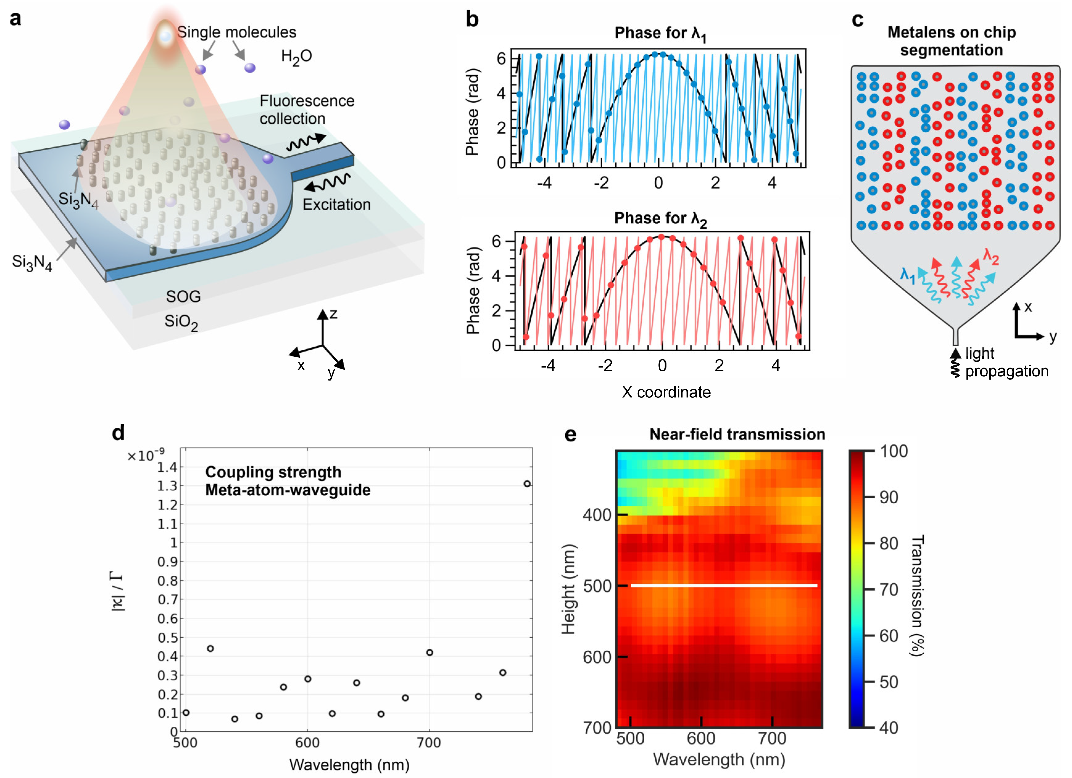
Figure 2.
Focal point overlap comparison of the dual-wavelength and chromatic metalenses on waveguide. (a) Point spread function (PSF) of segmented metalens for ATTO 490LS fluorescence detection at 500 nm and 660 nm. (b) PSF of single-wavelength metalens at 500 nm and 660 nm. (c) PSF of segmented metalens for Alexa 555 fluorescence detection at 520 nm and 550 nm. (d) PSF of single-wavelength metalens at 520 nm and 550 nm. (e) PSF of segmented metalens for APC-Cy7 fluorescence detection at 650 nm and 780 nm. (f) PSF of single-wavelength metalens at 650 nm and 780 nm. The color bars depict optical field intensity.
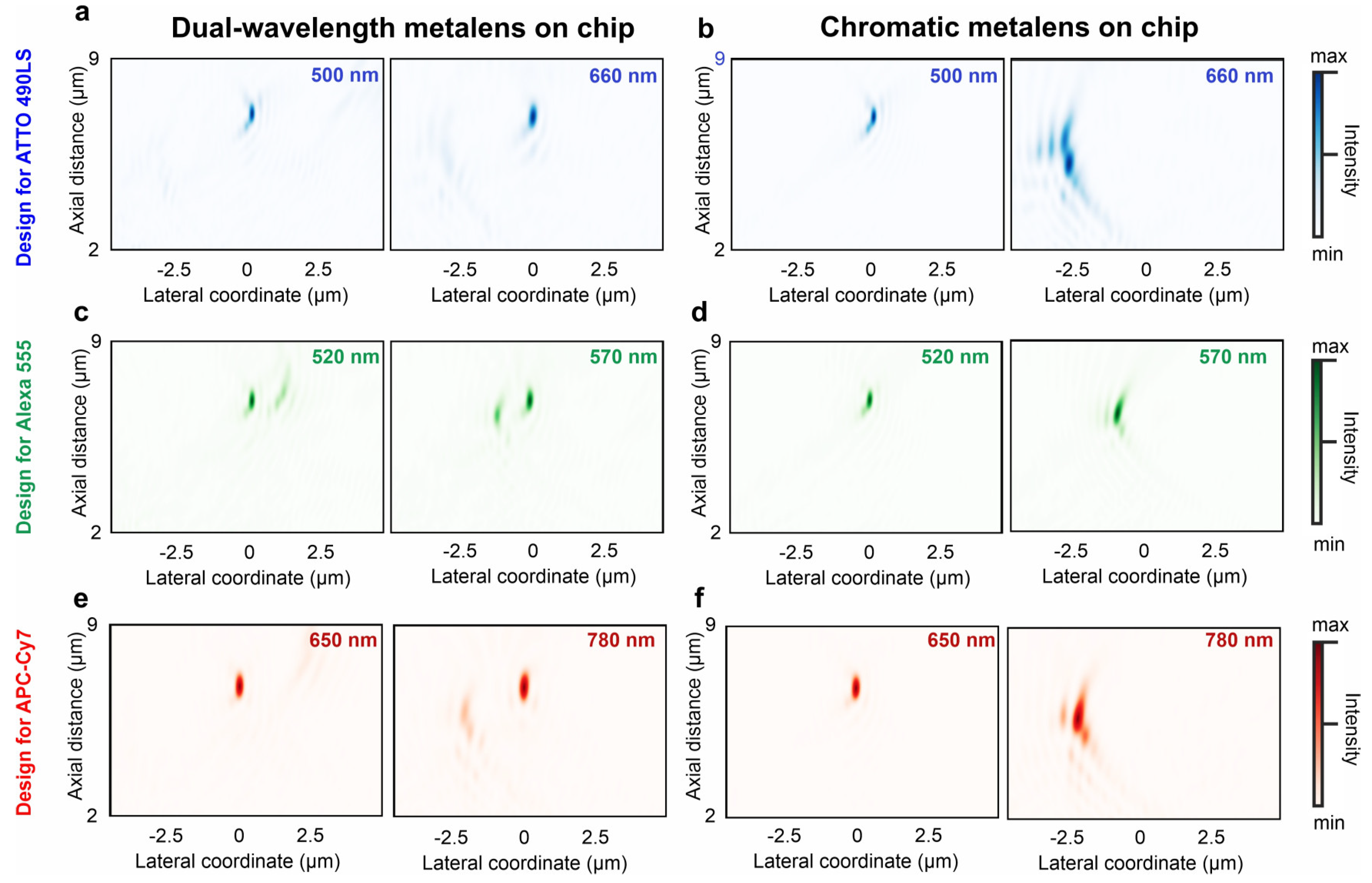
Figure 3.
Lateral PSF and linear intensity profiles of dual-wavelength metalenses on chip. (a) Lateral PSF of metalens for ATTO 490LS fluorescence detection at 550 nm and 660 nm. (b) Horizontal cut off the images in (a). (c) Axial intensity profiles of the metalens for ATTO 490LS fluorescence detection at 550 nm and 660 nm. (d) Lateral PSF of metalens for Alexa 555 fluorescence detection at 520 nm and 550 nm. (e) Horizontal cut off the images in (d). (f) Axial intensity profiles of the metalens for Alexa 555 fluorescence detection at 520 nm and 550 nm. (g) Lateral PSF of metalens for APC-Cy7 fluorescence detection at 650 nm and 780 nm. (h) Horizontal cut off the images in (g). (h) Axial intensity profiles of the metalens for APC-Cy7 fluorescence detection at 650 nm and 780 nm.
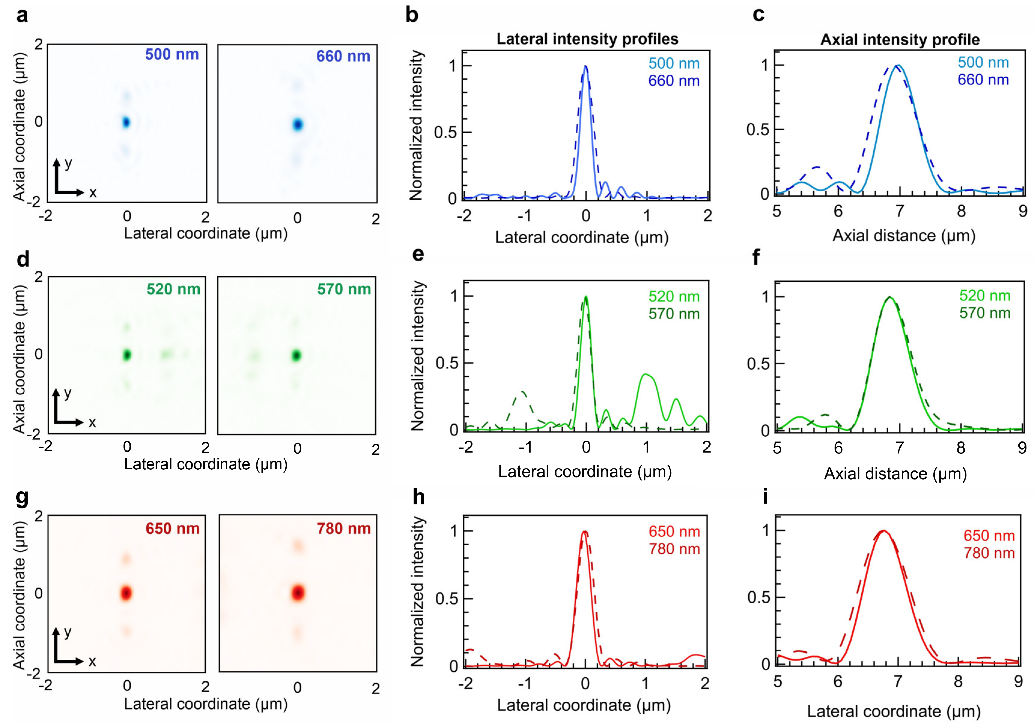
Figure 4.
Molecule detection efficiency under epi-fluorescence configuration. Absorbance and fluorescence spectra of (a) ATTO 490 LS, (b) Alexa 555, (c) APC-Cy7. The solid line spectra denote absorbance, while the dashed-line spectra are referred to emission. Solid lines denote design excitation wavelength, and the shading indicates the simulated collection band by the metalens. The spectra Computed molecule detection efficiency with dual-wavelength metalenses designed for (d) ATTO 490 LS, (e) Alexa 555, (f) APC-Cy7.
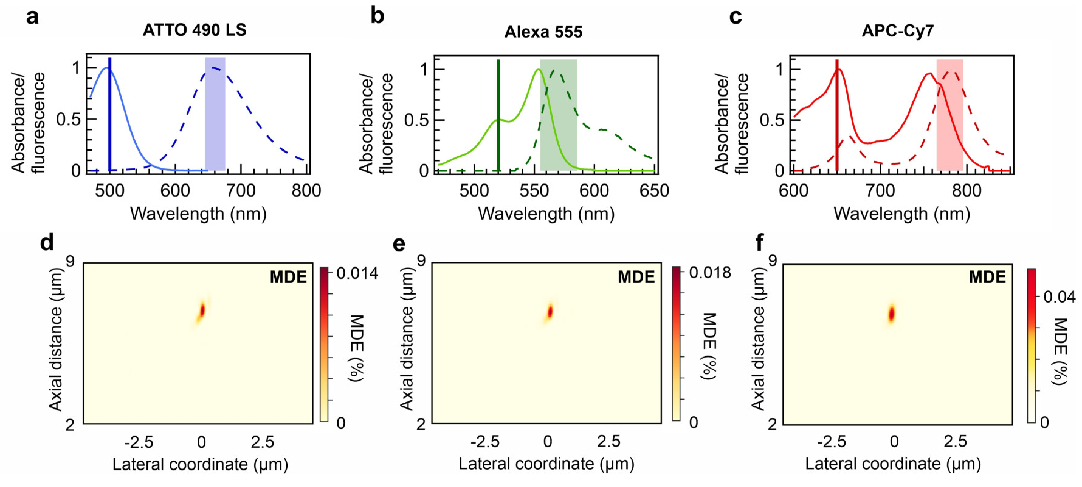
Figure 5.
Metalens-based diffusion autocorrelation functions for molecules of interests. Simulated FCS data with fitting curves is represented for (a) ATTO 490 LS, (b) Alexa 555, (c) APC-Cy7. The fit funcitons correspond to a 3D diffusion FCS model.
Figure 5.
Metalens-based diffusion autocorrelation functions for molecules of interests. Simulated FCS data with fitting curves is represented for (a) ATTO 490 LS, (b) Alexa 555, (c) APC-Cy7. The fit funcitons correspond to a 3D diffusion FCS model.
Disclaimer/Publisher’s Note: The statements, opinions and data contained in all publications are solely those of the individual author(s) and contributor(s) and not of MDPI and/or the editor(s). MDPI and/or the editor(s) disclaim responsibility for any injury to people or property resulting from any ideas, methods, instructions or products referred to in the content. |
© 2024 by the authors. Licensee MDPI, Basel, Switzerland. This article is an open access article distributed under the terms and conditions of the Creative Commons Attribution (CC BY) license (http://creativecommons.org/licenses/by/4.0/).
Copyright: This open access article is published under a Creative Commons CC BY 4.0 license, which permit the free download, distribution, and reuse, provided that the author and preprint are cited in any reuse.


