Preprint
Article

This version is not peer-reviewed.

Design and Simulation of a Novel Modular Converter-Transformer for AC/DC, DC/AC and DC/DC Operations

A peer-reviewed article of this preprint also exists.

Submitted:

11 November 2024

Posted:

15 November 2024

You are already at the latest version

Abstract

This manuscript describes the research and the development of a novel family of modular AC/DC, DC/AC and DC/DC converters for high voltage interconnections between AC and DC lines or between two DC lines. Such devices are bidirectional and they integrate a three-phase power transformer. The relationship existing between AC and DC voltages in each module for rectifier and inverter operations is analogous to the one set in single-phase thyristor bridges. Due to the novelty of this topic, a low-voltage, low power prototype was sized to make a first validation of its predicted behaviour. This converter should realize all the operating modes allowed by the new family of devices, namely, AC/DC, DC/AC and DC/DC conversions. Its rated phase voltage is 230 V rms and it should be able to carry at least 1 kW. Thus, a switching model of the device was realized first. The simulated behaviour of this prototype is deeply discussed in this paper during steady-state, transient and DC-fault operations.

Keywords: 
;  ;  ;  

1. Introduction

High-voltage DC (HVDC) interconnections became interesting solutions in several countries worldwide for sub-sea and/or long transmission lines ( 600 700 k m ) in the last 20 years, due to their economical convenience and several technical advantages with respect to traditional three-phase AC solutions [1,2]. Among all the possible aspects in favour of long DC lines versus AC ones, it is worth mentioning the theoretical absence of skin effects on the conductors, limited harmonic content in DC quantities, no issues related to quarter-length lines and reduced number of conductors in each interconnection (i.e., two or even one active conductors instead of three). Therefore, researches in power electronics focuses on the design of converters working as interfaces between AC and DC grids or directly among DC ones. These devices should aim to be efficient, safe, flexible and must provide strong reduction of both the harmonic distortion on the AC side and the ripple on the DC one.
After the first studies and applications with conventional two-level converters, new solutions started to be investigated based on three- or multi-level solutions [3,4,5]. Indeed, the need for large passive filters was an issue with two-level devices to reduce harmonic pollution. In particular, modular multilevel converters (MMC) became a very appreciated solution by the scientific community due to their applicability as well as scalability for several voltage levels [6]. The literature reports many case studies involving the applications of such devices, e.g., recharging stations [7], battery management systems [8] and traction [9,10] on electric vehicles [11] as well as interfaces for HVDC interconnections [12,13,14,15,16]. It goes without saying that multi-level converters in general ensure better approximations of sine waves with increasing number of levels, without the need for rising the switching frequency too much. On the other hand, they may have higher costs associated with the required semiconductors compared to two-level solutions, even though each power switch has a nominal voltage which is inversely proportional to the number of installed modules. Hence, a trade-off must be found between the reduction in size of passive filters, the increase in number of switches in the converter and their associated costs.
Additionally, another big challenge in DC interconnections is the clearance of DC faults. This is still the subject of several researches carried out by the scientific community due to the intrinsic lack of any zero crossing in DC currents. Hence, typically large energy dissipation are associated with clearance events and traditional AC circuit breakers cannot be used to this aim during such faults. The literature offers solutions like solid state breakers [17,18], hybrid breakers (i.e., with both semiconductors and mechanical switch) [19,20] and MMC converters with fault blocking capabilities [21]. With this background in mind, Terna, the Italian Transmission System Operator (TSO), deposited a patent proposing a new family of bidirectional Converter-Transformers (CTs) capable of working as Rectifiers AC/DC, Inverters DC/AC and DC/DC Converters [22,23]. These new devices have a multi-level and modular characteristics. However, they differ from MMCs due to the absence of batteries or capacitors as energy storage elements in each module. Moreover, these converters are characterized by the capability of transforming DC fault currents into AC ones, allowing the exploitation of traditional AC protections for DC fault clearance.
Specifically, this paper shows the working principles of this new family of devices and reports the sizing and the first simulations of a low-voltage, low-power prototype. The digital twin of the physical device is based on a switching model of the electrical system, and it is aimed to prove the applicability of the idea proposed in the patent. Moreover, a real prototype is created based on the simulation results obtained during this research. In particular, the device could be operated in all three different working operations: namely, AC/DC, DC/AC and DC/DC conversions. The realization of the actual converter and the experimental test campaign are still ongoing while writing this paper.
Hence, the manuscript is organized as follows: an overview of the working principles, the main equations linking DC and AC voltages for this family of device and the fault clearing strategy are reported in Section 2. Then, Section 3 explains how the prototype was sized and shows how its switching model was realized. Section 4 reports the results for several steady-state and transient operations and for some sensitivity analyses as well. In particular, emphasis is put on the simulation runs showing the fault clearance capability of the device. Finally, conclusion is drawn.

2. Structure and Main Equations of the New Family of CTs

2.1. Topology of the Device

The family of converters described in patent [22] are characterized by the presence of a multi-winding power transformer, which primary is directly connected to the AC grid for AC/DC and DC/AC operations. Thus, it must work at grid frequency, namely 50 or 60 Hz . Such transformers should have three primary windings and 3 × M secondaries (namely, M is the number of secondaries in each phase forming a M-level converter). Every power module has two couples of terminals, thus, forming one AC port and a DC port. The AC side is connected to a secondary winding with a one-to-one correspondence, as shown in Figure 1. All the elementary power cells are then cascaded connecting their DC terminals in series. This peculiar arrangement determines a DC bus and a three-phase AC port at the primary terminals of the transformer for the whole device (see Figure 1). Therefore, the CT can be seen as an equivalent power transformer with time varying transformation ratio between the AC and DC ports.
Moving to the topology of the 3 × M power modules, it slightly depends on the adopted semiconductor technology and application. For high- and medium-voltage frameworks, Gate Turn-off Thyristors (GTOs) and Integrated Gate-Commutated Thyristors (IGCTs) are the best candidate switches. For medium- and low-voltage applications, Insulated-Gate Bipolar Transistors (IGBTs) can be used, whereas Metal–Oxide–Semiconductor Field-Effect Transistors (MOSFETs) are intended only for low-voltage applications. The peculiarity of all these cells is the presence of anti-series or anti-parallel switches to allow the bidirectional control of the device during DC/AC and AC/DC operations, as well as to block the current flow in specific directions through the switches: the arrangements for the switch technologies mentioned before are reported in Figure 2. It must be said that the arrangements reported in Figure 2 show discrete switches, but monolithic bidirectional switches [24] can be used as well to help improving the power density of the devices.
Regarding the DC/DC operation, a power transformer is foreseen as well. For this specific application, it should be multi-winding both on the primary and on the secondary sides, having an inverter and a rectifier stage. Namely, the input stage works as inverter, whereas the output one operates as rectifier. The two stages are cascaded in this configuration; overall, a device working as DC/DC converter should have two DC ports. The frequency on the AC side of the modules can be much higher than 50 or 60 Hz , since no interface with AC grid is foreseen. Therefore, the geometrical size of the transformer can be much smaller than in inverter or rectifier operations.

2.2. Modulation Strategy

The topologies proposed in Figure 2 enable bidirectional power flow to the CTs. As already stated, the eight electronic switches are never on at the same time. Indeed, the four semiconductors labelled with letters “a” or “b” (as reported in Figure 2) can be enabled or disabled through two signals Ga and Gb. The first activates the four modules involved in the inverter operation when set to a logic high value, whereas Gb is turned on to start rectifying operations. Then, the effective dynamic variation of the transformation ratio of the CT between its AC and DC ports is a consequence of the turn number in the power transformer and the modulation strategy adopted to drive the power electronics. This last is analogous to the nearest level control (NLC) used in MMCs [13]. Namely, three reference sinusoidal signals v e , 1 t , v e , 2 t , v e , 3 t with 2 / 3 π mutual phase displacement and synchronization with the AC grid (if connected) are compared with constant thresholds V h , with h = 1 , , M associated to each module. The v e , i t are defined as:
v e , i t = V e sin ω t + φ i + φ e
with φ i = 0 , 2 / 3 π , 2 / 3 π for the considered phase i = 1 , 2 , 3 . φ e can be set 0 to provide a phase displacement between the grid voltage and the excitation signal: the aim is to obtain a regulation effect at the output terminals for the three operations. As will be shown later in this paper, the effect of variations on φ e is similar to the one obtained controlling firing angles in thyristor bridges. Moreover, the duty cycle of the modules can be varied by changing the peak value V e .
Based on the result of the comparisons, couple of switches on each module are activated at a time. Three states are allowed on a module: direct, reverse and bypass as shown in Figure 3. The direct configuration provides a connection between AC and DC terminals such that the positive half-sine wave of AC signals is brought on DC terminals on each module during rectifier mode. Analogously, the same switch arrangement is exploited to synthesize the positive half-waveform of the AC quantities in inverter mode. Reverse state is similar to the direct one, but with a flipped connection of the AC and DC terminals. Therefore, the negative side of sine waves are mirrored with respect to the x-axis and reported on the DC terminals during rectifier operations. Instead, negative side of AC waveforms are generated using reverse state in inverter operation mode. Finally, bypass sate is a short-circuit of the DC terminals and, in principle, it should be used both to shape the AC quantities and to control the power flowing through the device.
These three states are applied sequentially according the switching table reported in Table 1. This schedule is configured to include small ranges δ to allow smooth transitions between direct, inverse and bypass states, if needed. Namely, three swhitches are on for a short period of time to prevent abrupt transients between two following states. It can also be noted that all the switches are off in idle mode and the current circulation is prevented in any direction. Figure 4 reports an example of a comparison between a generic v e , i t and constant threshold V h with δ = 0 and φ e = 0 to show how the modulation is operated. It can be observed that modules can be stressed differently based on the specific value of V h associated to each of them. To provide a better exploitation of the power electronics, dynamic permutations of these constant values over the modules can be realized.

2.3. Analytical Model of the Devices

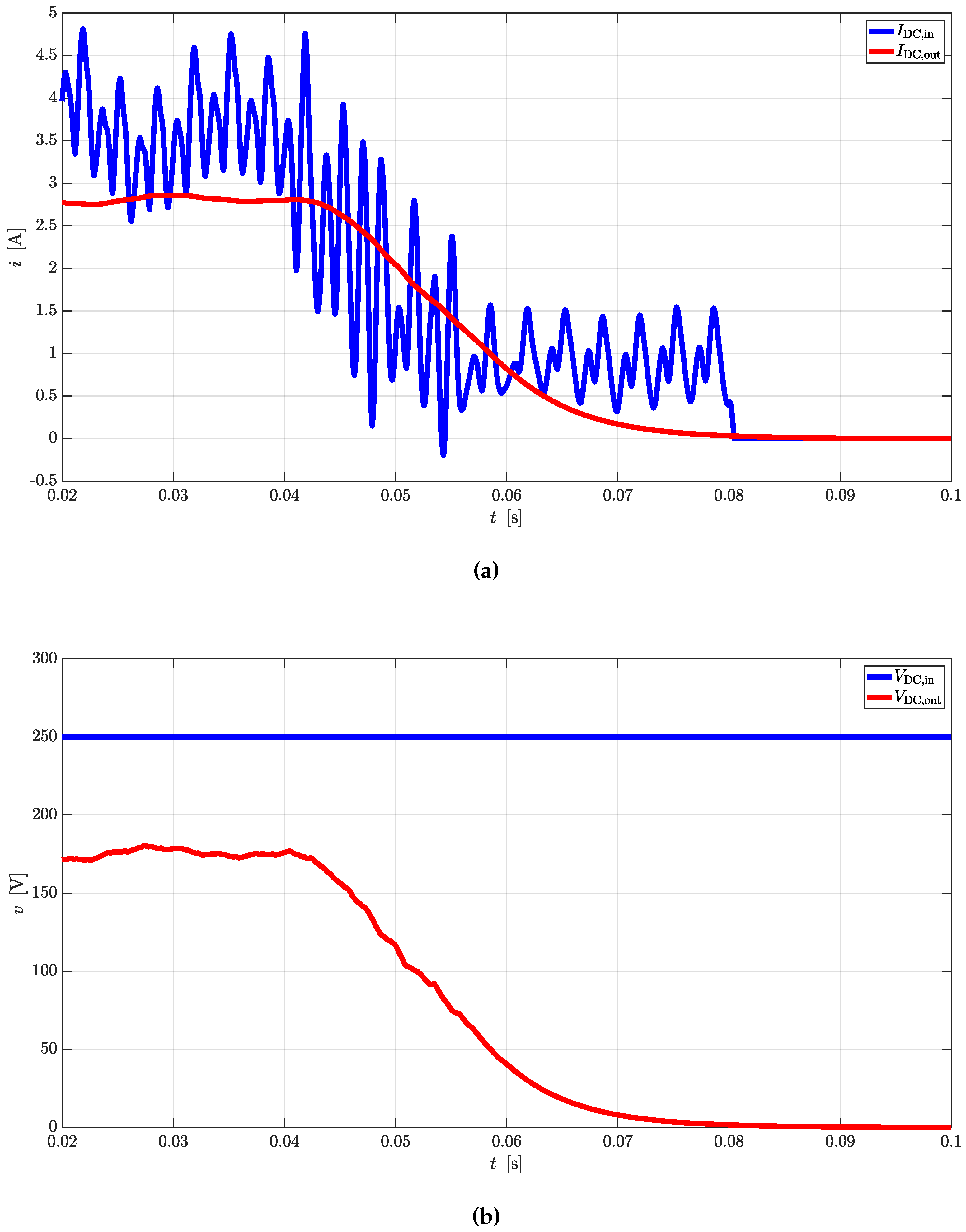
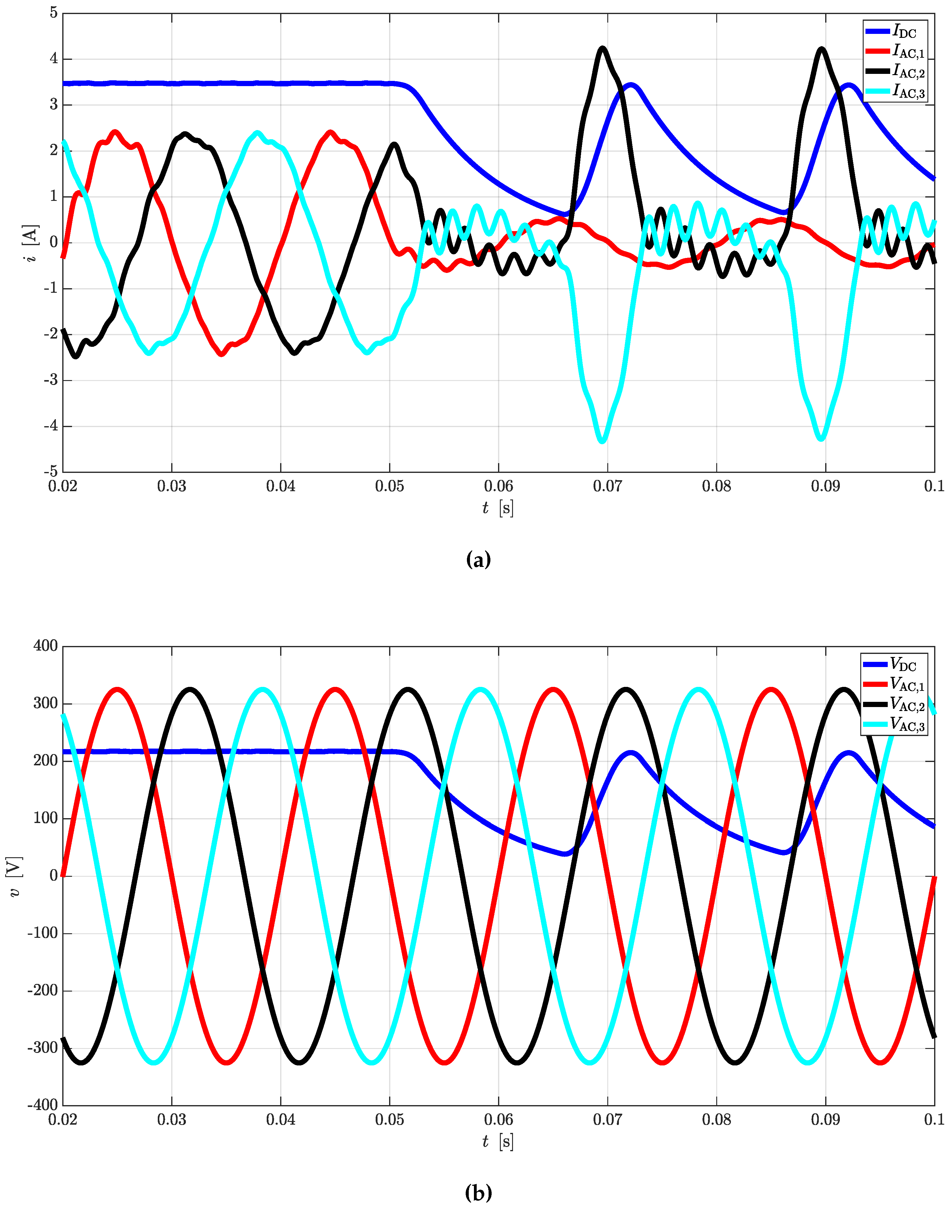
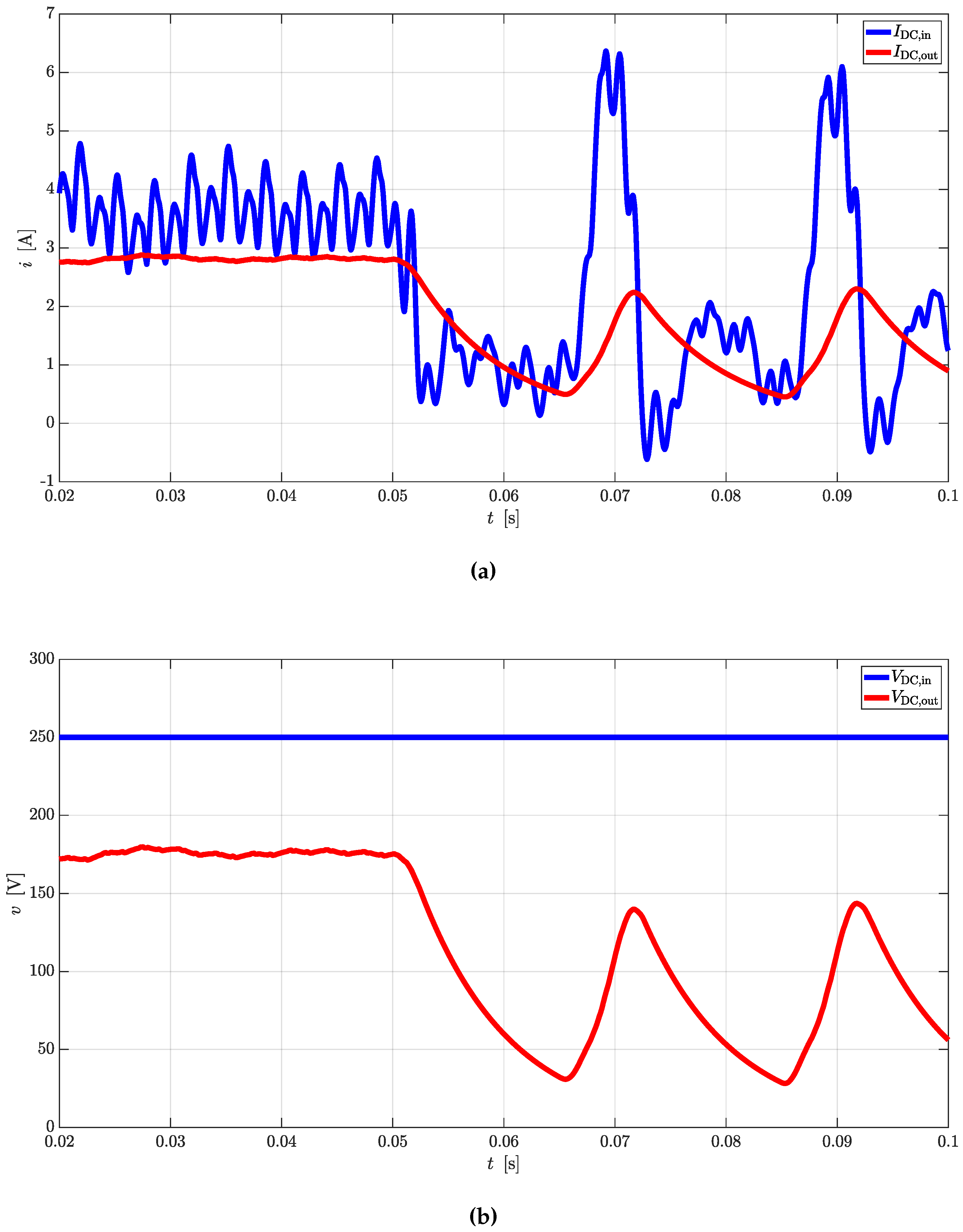
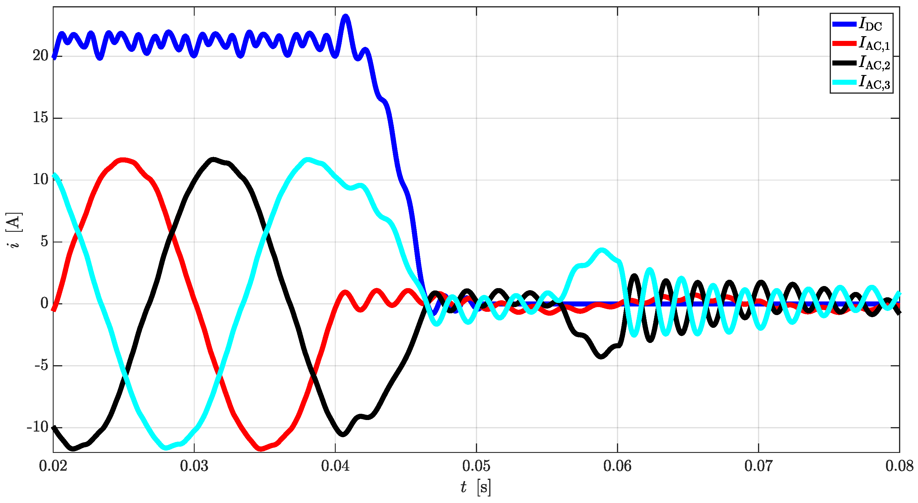
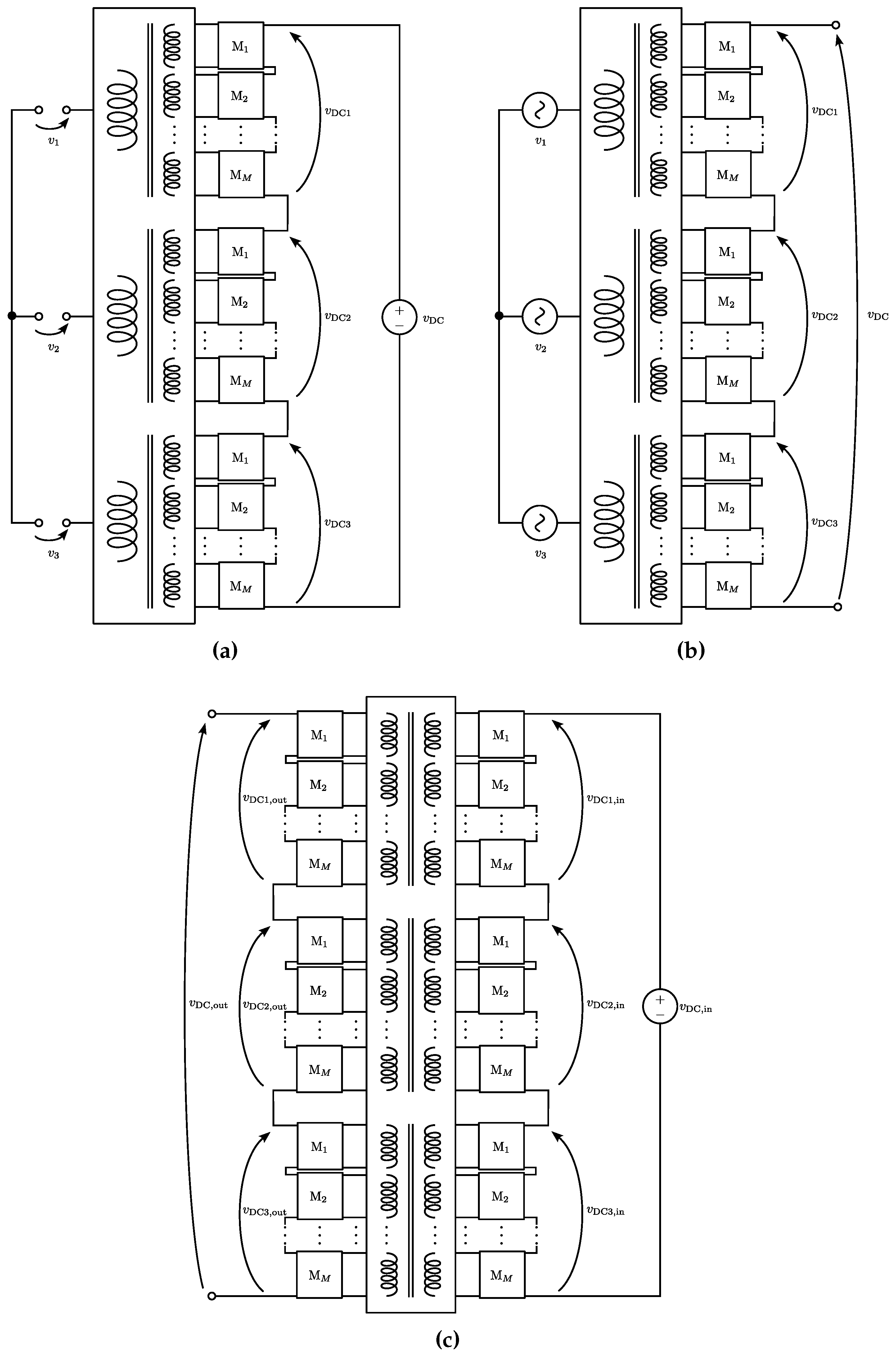
Simple equations can be derived to link AC quantities with the DC ones for rectifier and inverter operations. In case CTs are used as DC/DC converters, the same equations can be cascaded to provide valid estimations.
The easiest relationship that can be formalized is based on a dynamic transformation ratio k t defined as:
k t = h = 1 M N c h t N p
where c h is a function of time (typically a combination of square waveforms) that depends on the specific state of the h-th module. Namely, it can assume the values 1 , 0 , 1 for reverse, bypass, direct states, respectively, assumed at the specific time instant t based on Table 1. N is the number of turns of each secondary winding (assuming all of them are equal) connected to the h-th module while N p is the total number of primary turns. Hence, the primary voltage v p , i t = 2 V p sin ω t + φ i and the DC voltage v DC , i t on each phase i can be linked as follows
v DC , i t = k t v p , i t
In three phase systems, the waveform of the overall DC voltage v DC t can be computed as:
v DC t = i = 1 3 v DC , i t
Namely, the combination of equations (2), (3) and (4) provides an indication of the harmonic content in the involved quantities, assuming that 1) the supply side is a pure sine-wave or a perfect constant, 2) the switching operations are ideal and 3) all the reactive elements in the system are negligible. It can be noted that this approach has many limitations. The most important one is that k t is a piece-wise function and it may not be easy to manage when the number of modules is very large. From this observation, a simpler relationship between AC rms voltage and DC mean value can be formalized. To this aim, a rectifier operation of the CTs is assumed; thus, the starting point is the expression of the DC voltage v DC 1 t associated to phase 1 (i.e., φ i = 0 ) through a piece-wise function dependent on the threshold levels V h , h = 1 , 2 , , M and δ = 0 :
v DC , 1 t = 2 V s sin ϑ for φ e ϑ arcsin V 1 V e + φ e 2 2 V s sin ϑ for arcsin V 1 V e + φ e < ϑ arcsin V 2 V e + φ e M 2 V s sin ϑ for arcsin V M V e + φ e < ϑ π arcsin V M V e + φ e 2 2 V s sin ϑ for π arcsin V 2 V e + φ e < ϑ π arcsin V 1 V e + φ e 2 V s sin ϑ for π arcsin V 1 V e + φ e < ϑ π + φ e
where ϑ = ω t = 2 π f t with f the fundamental frequency of v p , i (i.e., 50 or 60 Hz ), V s is the rms value of the secondary voltage of the multi-winding transformer, which can be computed from the rms value of the primary voltage V p and the constant turn ratio:
V s = V p N N p
Focusing on v p , i (which are the voltages applied on the terminals of the primary windings), they can be shifted and amplified with respect to the AC grid voltages v i depending on the connection adopted at the primary terminals of the transformer (i.e., star, delta or zig-zag). Hence, no relationship involving v i are investigated for simplicity in this paper. Considering the same system of equations, it is possible to write a relationship between V s and the mean value of DC voltage on each module, each phase and the whole DC bus as well. Indeed, starting from a piece-wise integration like the following one:
V DC m , h = 1 π arcsin V h V e + φ e π arcsin V h V e + φ e 2 V s sin ϑ d ϑ
it follows that:
V DC m , h = 2 2 π V s cos φ e cos arcsin V h V e = 2 2 π V s cos φ e 1 V h V e 2
Reminding the expression that links AC and DC voltages in ideal single-phase thyristor bridges [25]:
V d α = 1 π α π + α 2 V s sin ω t d ω t = 2 2 π V s cos α
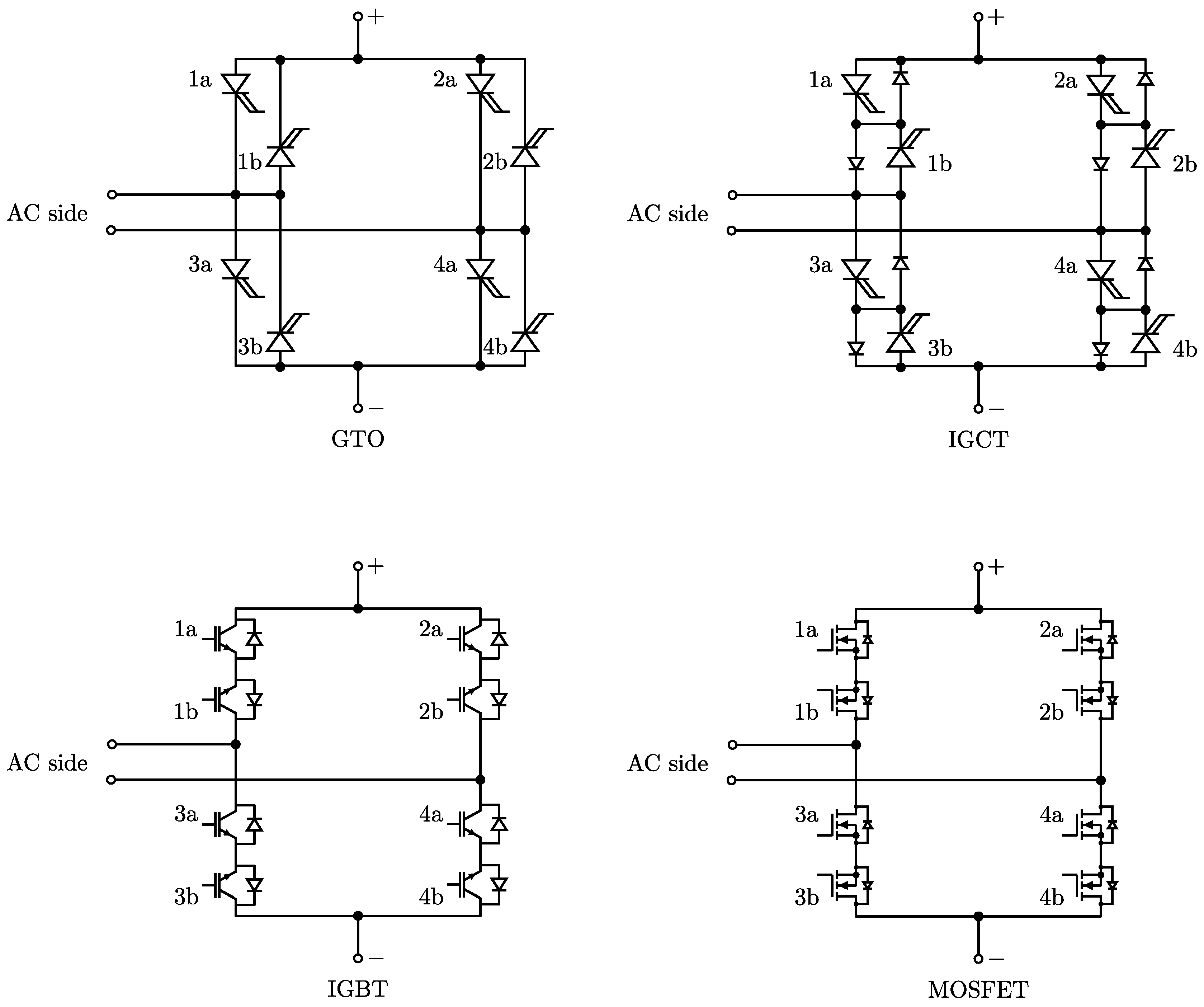
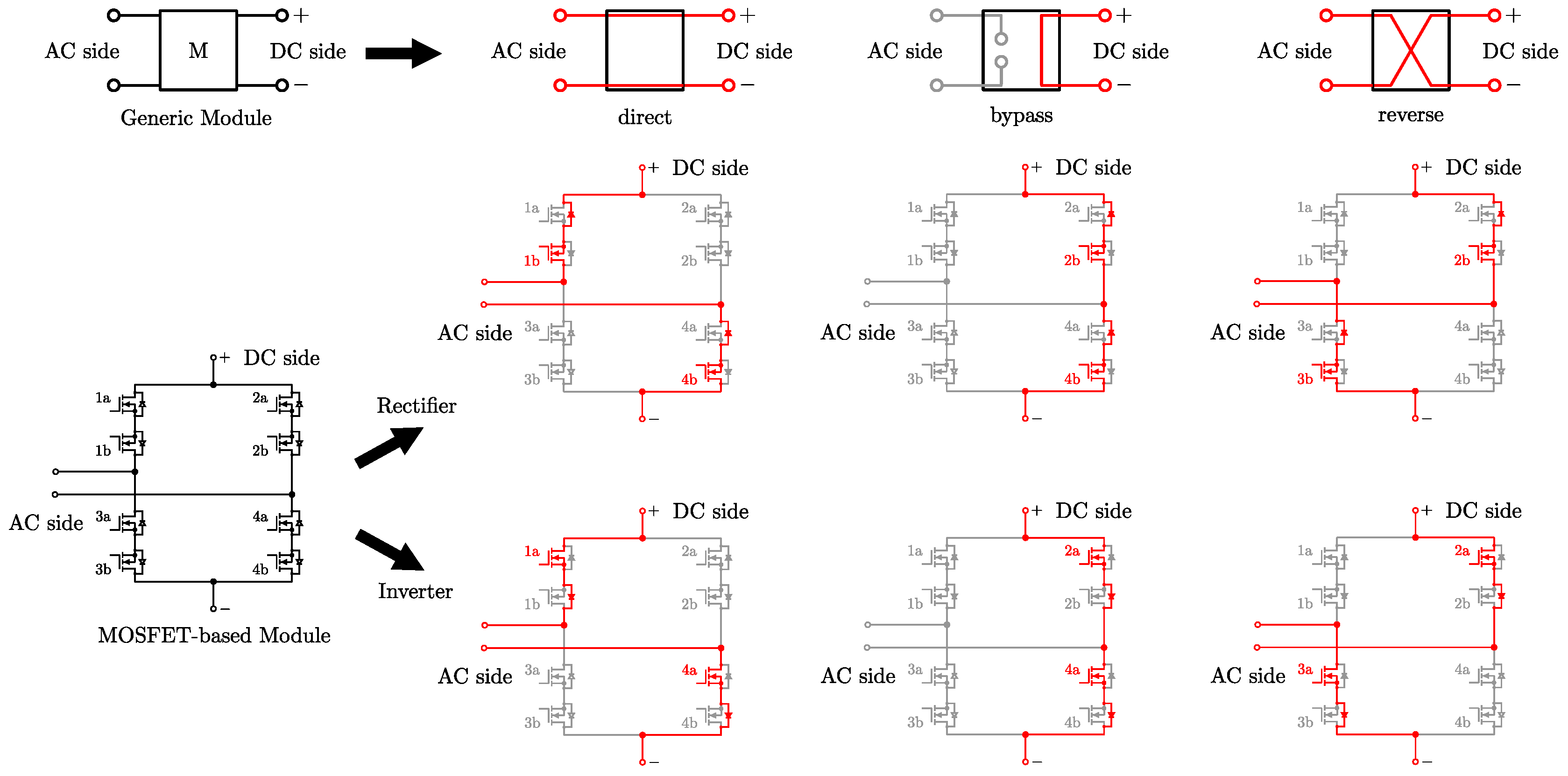
It can be noted that every module in the CT works exactly in the same way: φ e can be interpreted as the firing angle of an equivalent thyristor bridge, whereas the DC voltage is regulated through V h . Coming back to equation (8), the overall mean DC voltage of the device can be written as:
V DC m = 3 2 2 π V s cos φ e h = 1 M cos a h
with:
a h = arcsin V h V e
Equation (10) can be reversed to find V s as a function of V DC m , φ e , V e and the V h values. This relationship holds in absence of any loss:
V s = π 6 2 V DC m cos φ e h = 1 M cos a h
Voltage drops on the adopted switches can be included as well to provide more realistic estimations of V DC m and V s . For example, assuming that MOSFETs are used:
V DC m = 3 2 2 π V s cos φ e h = 1 M cos a h h = 1 M 2 R ds , on MOS I DCm + 2 V fw D
where R ds , on MOS is the on resistance of the mosfets, V fw D is the forward voltage of the diodes and I DCm is the average value of the DC current. The values of R ds , on MOS and V fw D can be extrapolated from the datasheet of the selected switches. Similarly, the relationship linking V s to V DC m becomes:
V s = π 6 2 V DC m M 2 R ds , on MOS I DC m + 2 V fw D cos φ e h = 1 M cos a h
It must be said that more accurate evaluations can be performed if the time dependent current is considered instead of its mean value. In that case, R ds , on MOS and V fw D should be updated based on the current flowing on each switch and its corresponding temperature. Instead, equations (13) and (14) exploit an average approach: at least two MOSFETs and two freewheeling diodes are always conducting in the whole period of AC quantities. However, the results are satisfactory and very simple to compute. In principle, losses related to the transformer can be included in the equation as well. The authors preferred to manage them separately and to deal with expressions involving power electronic components only.
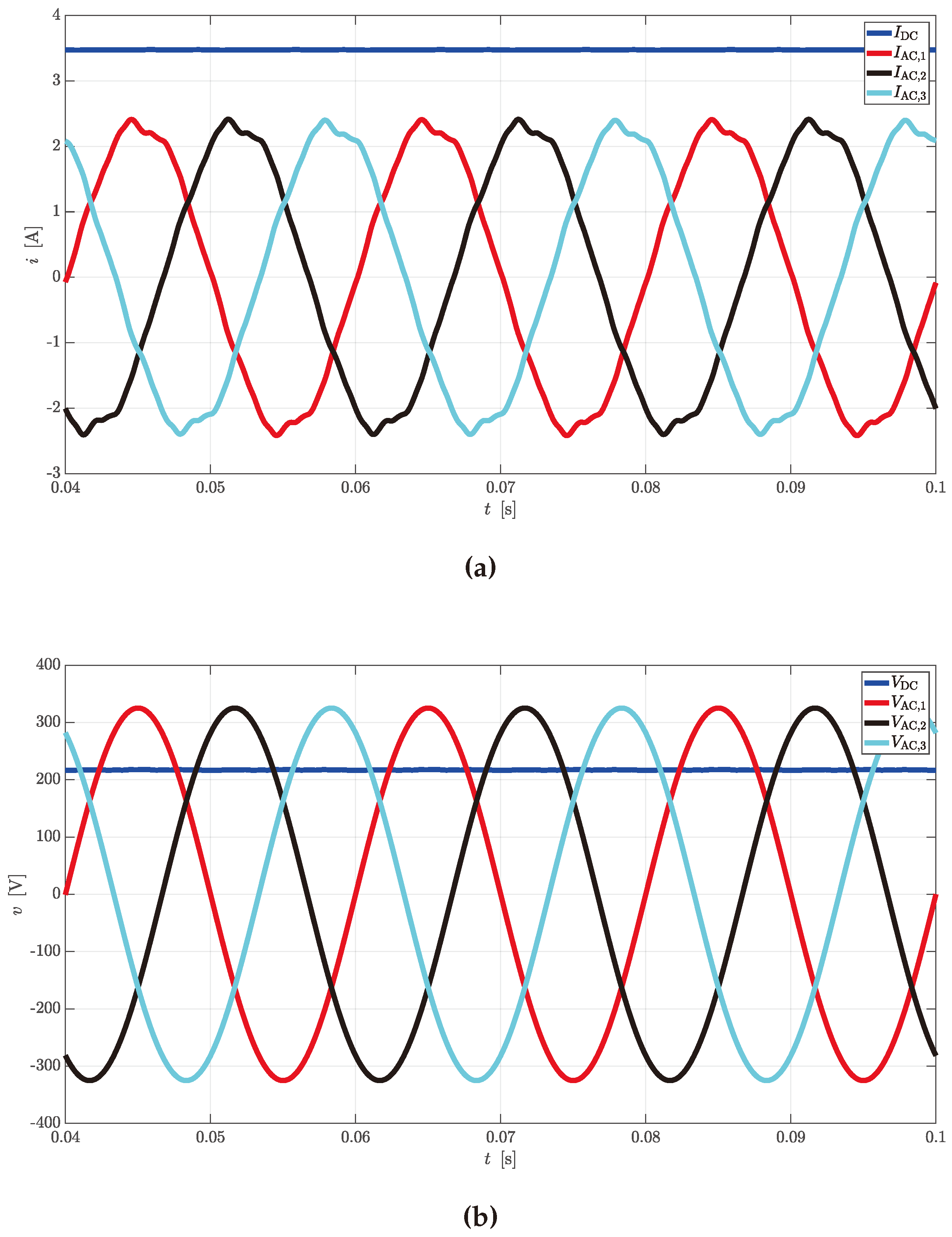
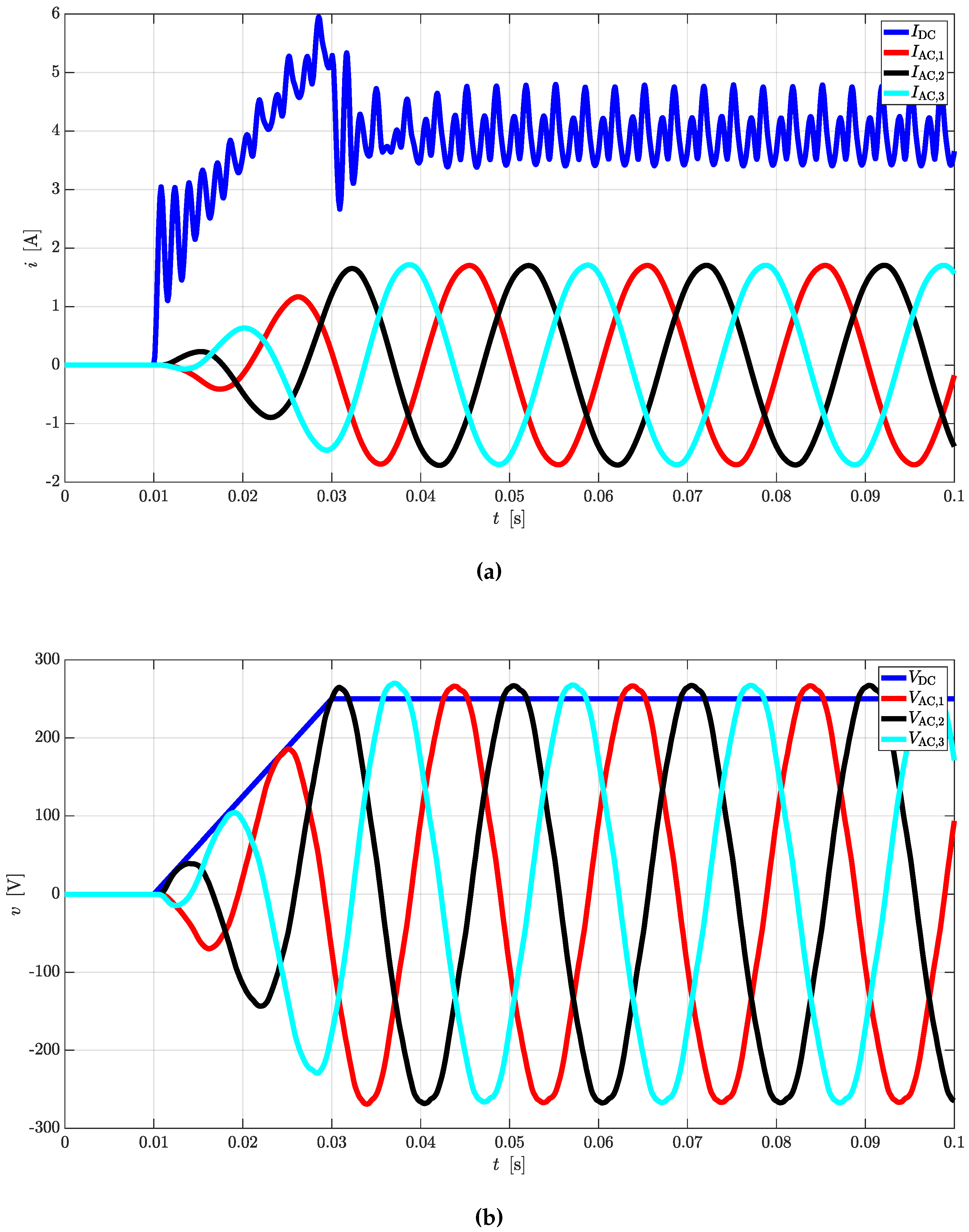
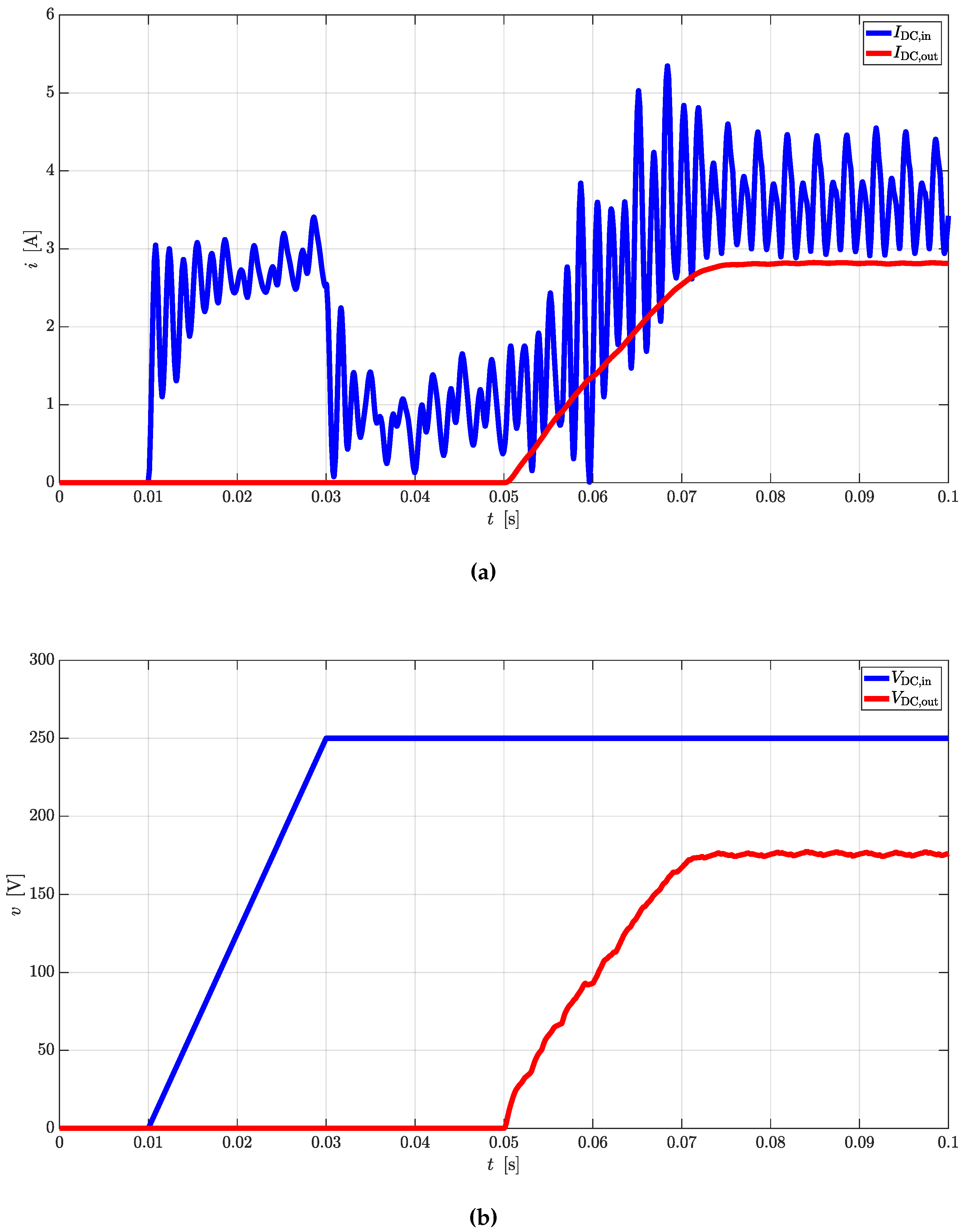
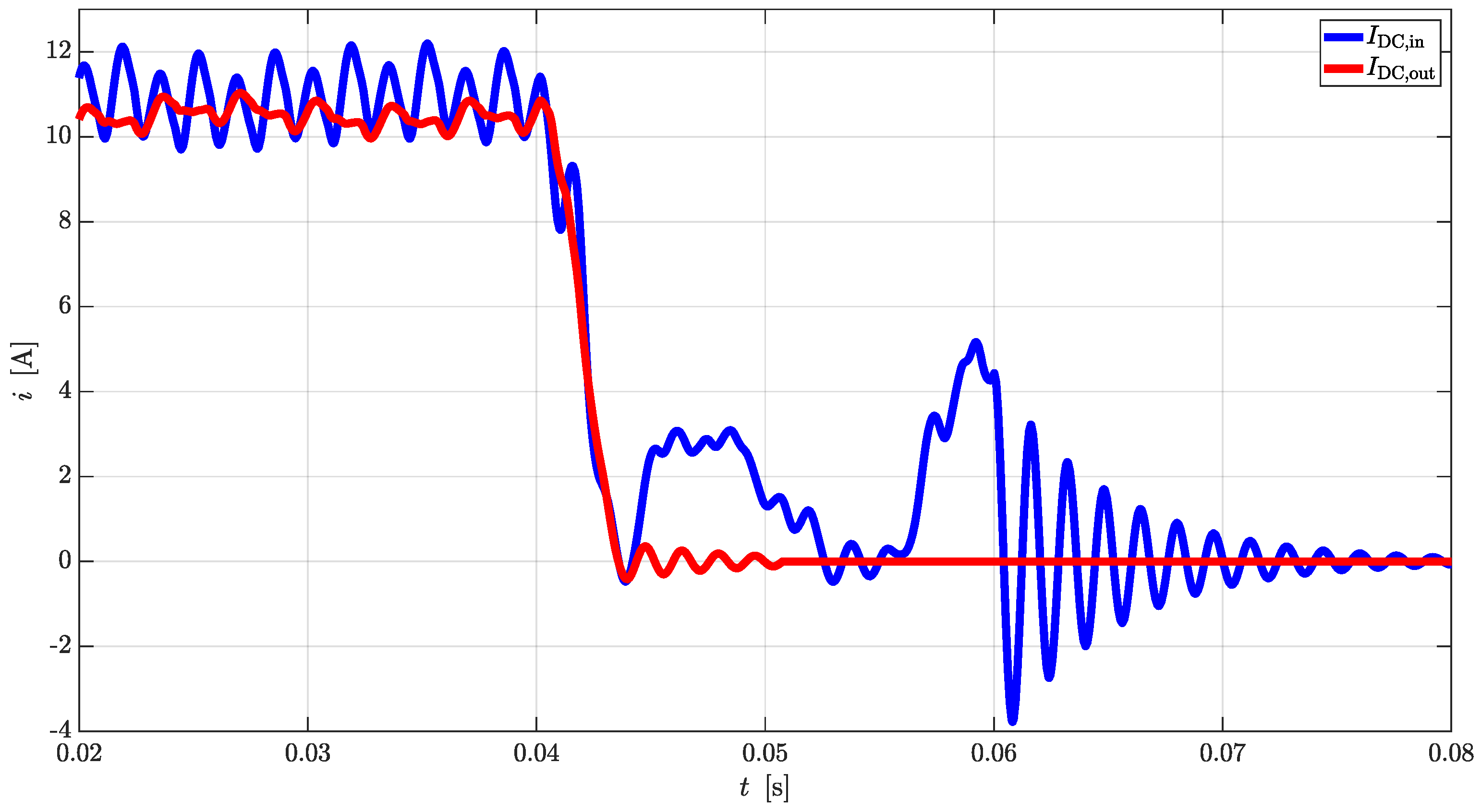
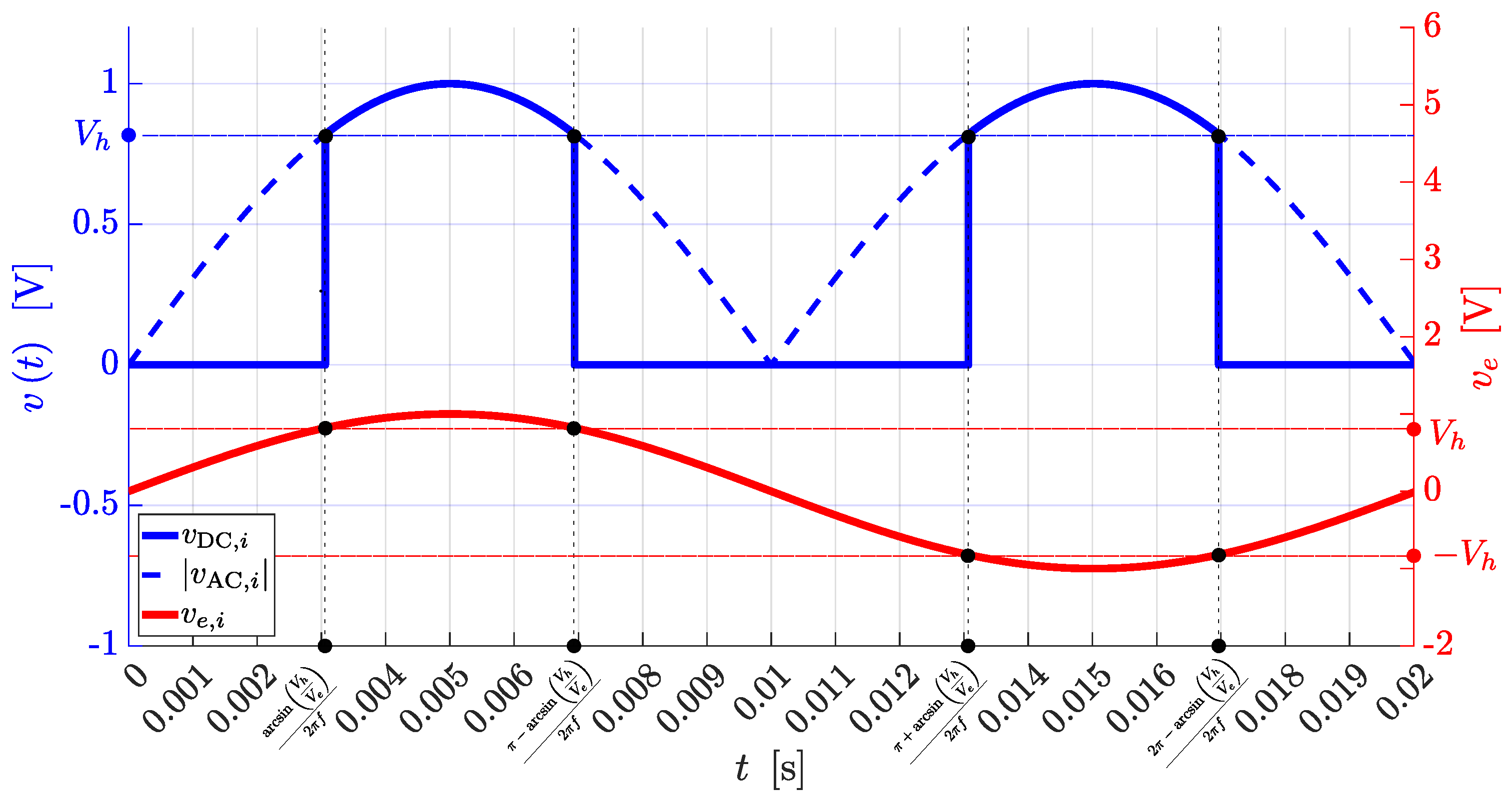
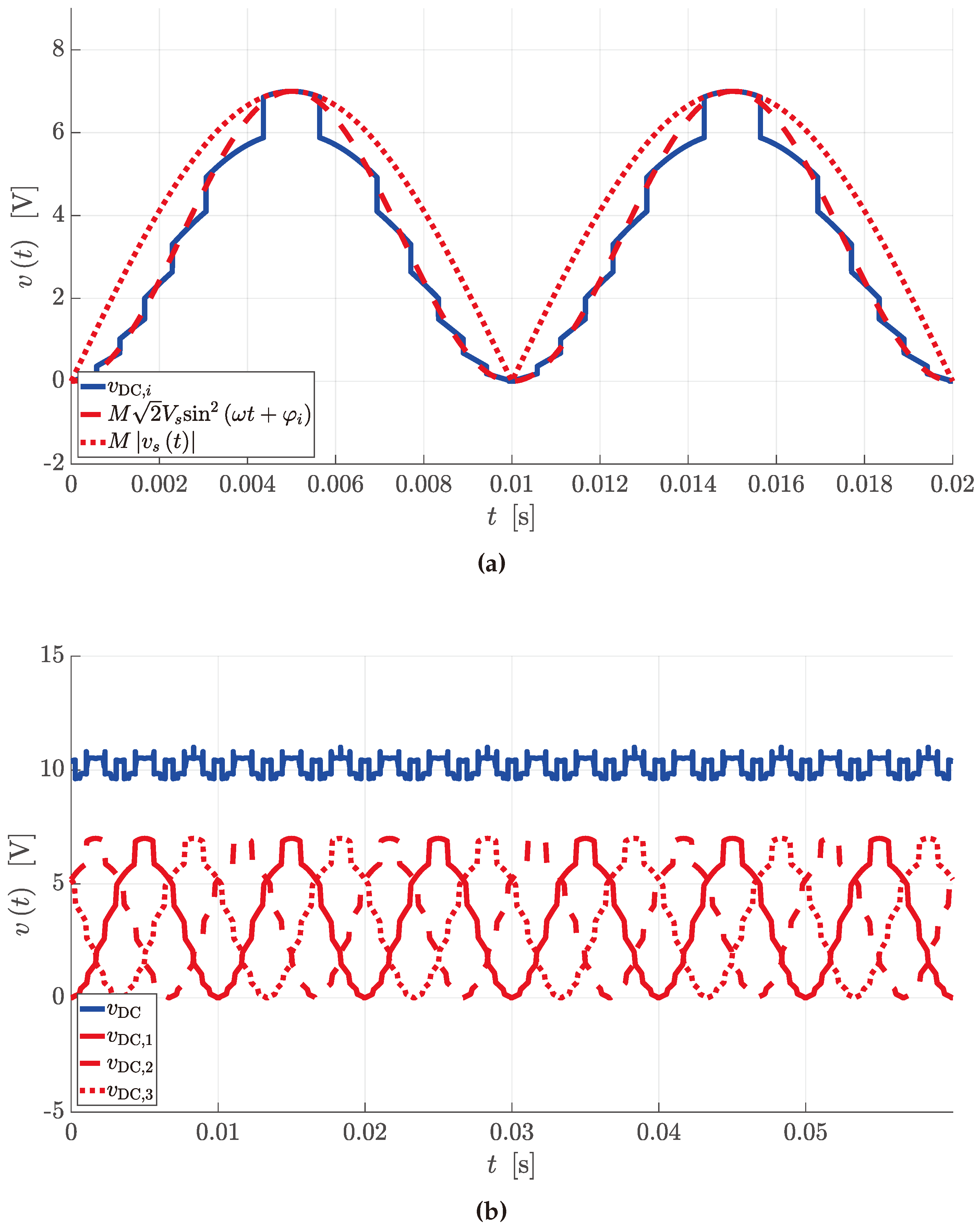
Figure 5 shows an example of ideal waveform for v DC , i t with 7 levels compared to the absolute value of the AC voltage with amplitude M 2 V s and the quadratic sine having the same peak-to-peak value. Equation (5) holds also for the other two phases and it can be proved that the rectified voltage on the i-th phase v DC , i can be approximated with:
v DC , i t M 2 V s sin 2 ϑ
if M . Figure 5 reports the ideal waveform v DC t obtained during a rectifier operation of the CT through the combination of the 7-level v DC , 1 t , v DC , 2 t and v DC , 3 t 
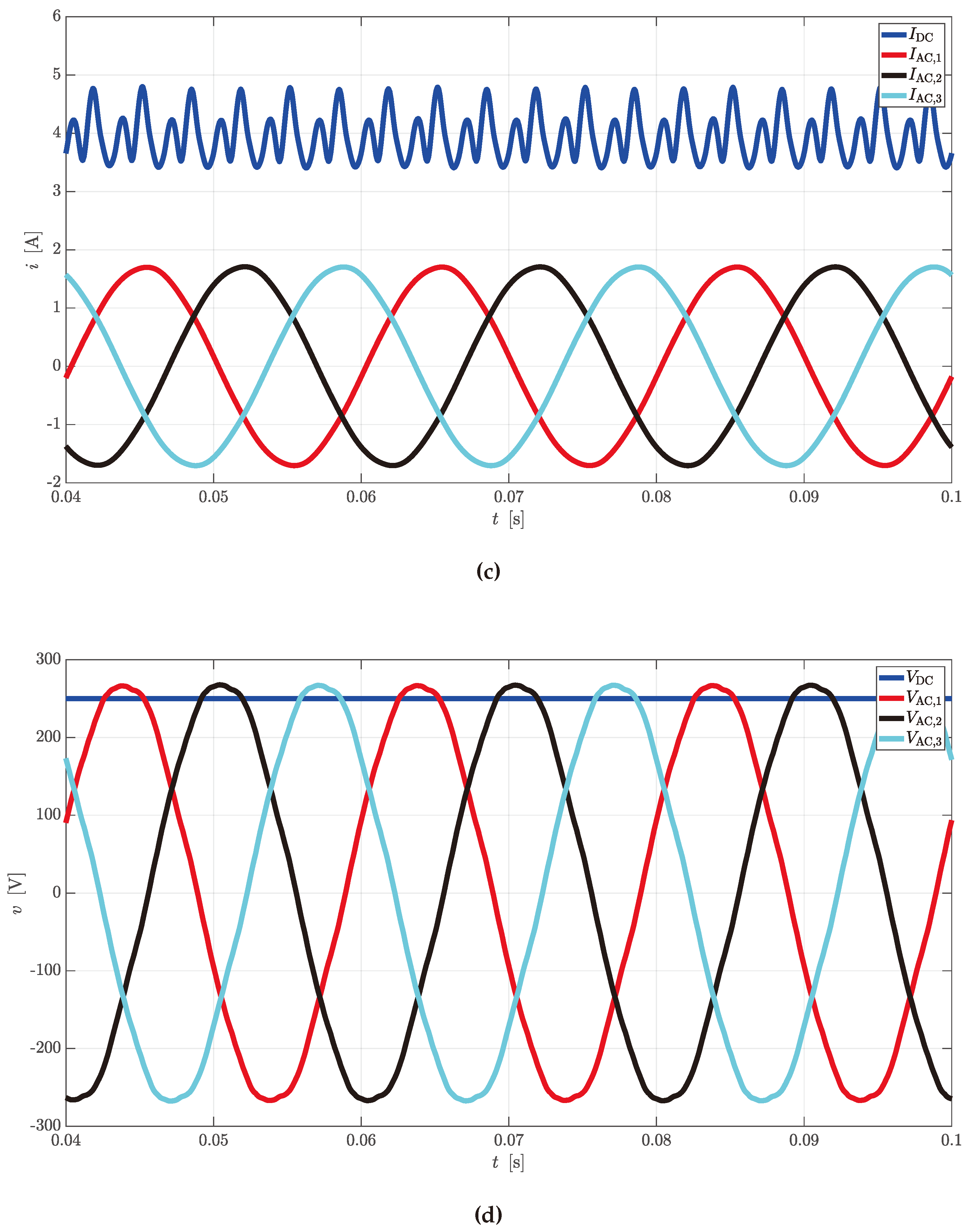
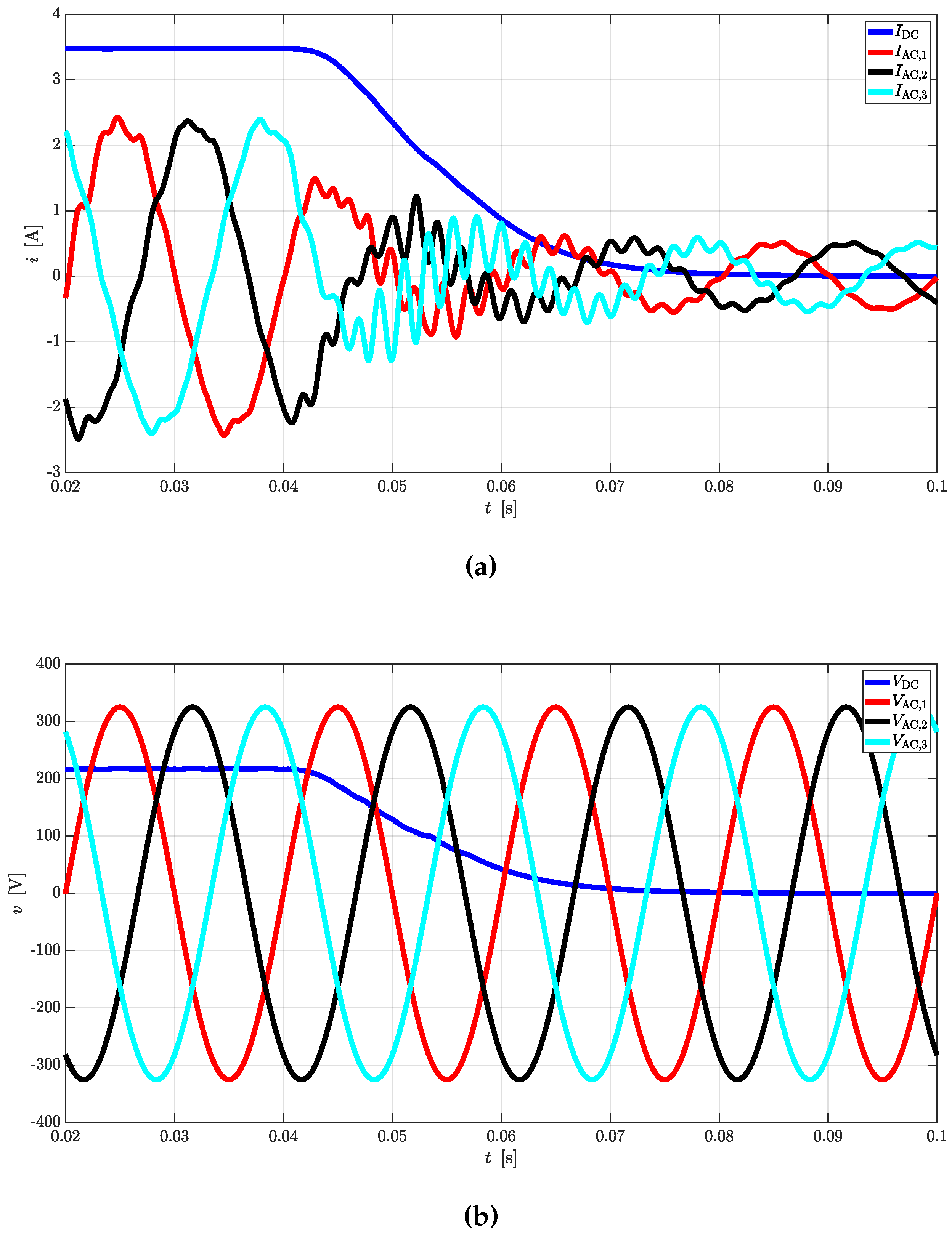
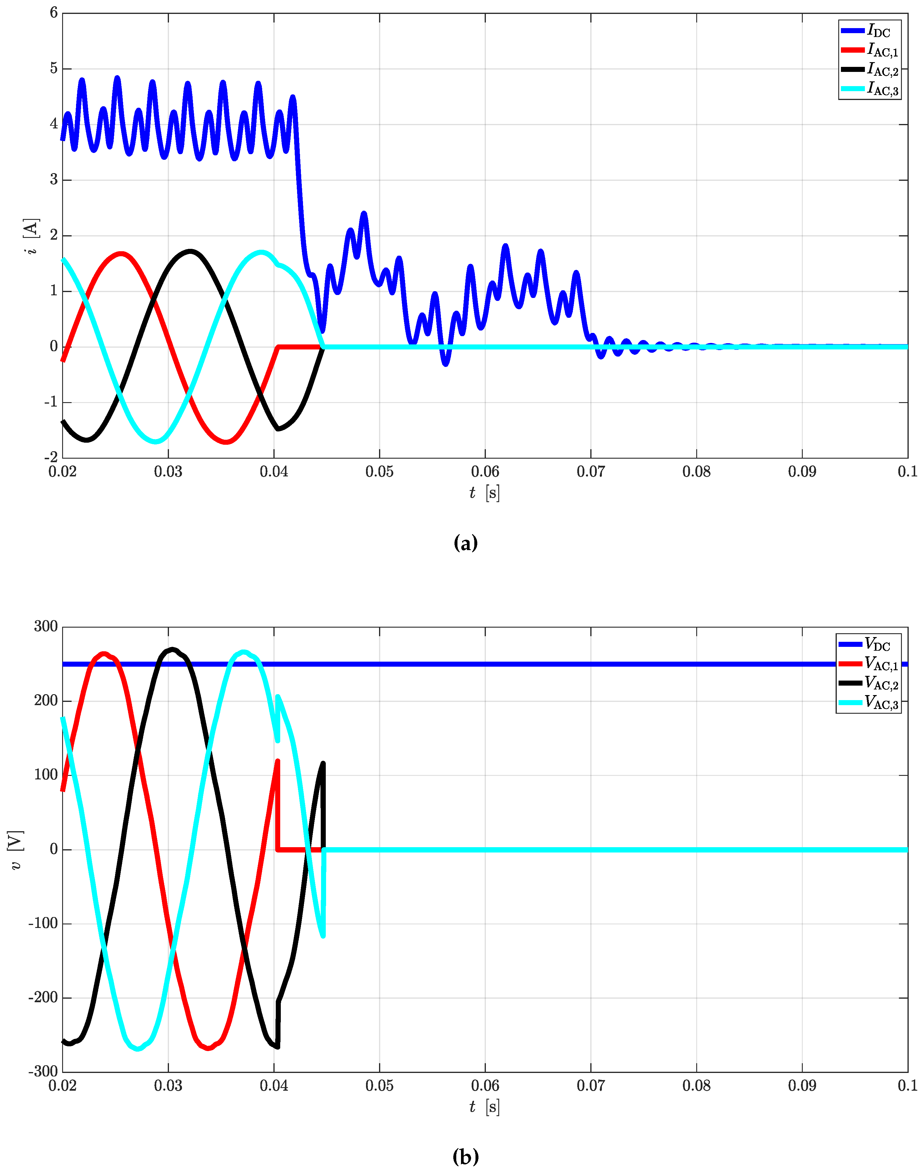
. It can be noted that the ripple is very limited even in absence of any passive filter. Ideal behaviors for inverter operations is such that v DC , 1 t , v DC , 2 t and v DC , 3 t are flipped with respect to the x axis every 10 m s . Thus, the ideal time evolution of v s , 1 t , v s , 2 t and v s , 3 t are obtained.

2.4. Fault Clearance Strategy

The previous sections described the modulation and the ideal behaviour of the device such that good rectifying and inverter performances are obtained. However, the peculiarity of this family of devices is that they permit DC fault clearance using conventional AC protections when the CTs are operated as rectifiers or DC/DC converters. To this aim, zero crossings are introduced in DC waveforms by freezing v e , i t causing a stop in the rectification process, as shown in Figure 6. Hence, AC voltages and currents are driven in the DC line if signals G a and G b are turned on and off accordingly. This feature allows to try a fault clearance attempt in correspondence of the first zero-crossing of the DC current: in case the fault is still not extinguished, other opening operations can be carried out in the following zero crossings. An example of successful clearance at first zero crossing is shown in Figure 6. It goes without saying that the CT operation with frozen v e , i cannot last too long, as the three phase side shows big unbalances and, possibly, may even behave as a two-phase system. Thus, this working mode is intended to last few milli seconds only in case of faults on the DC side or for shutting the system down when working as rectifier or as a DC/DC converter. During inverter operations, DC faults are supposed to be solved by the rectifier converter placed on the other side of the line, assuming that the DC grid has no meshes. Indeed, simulations proved that the freezing strategy has no beneficial effects on DC fault clearance in such cases.

3. Design and Switching Model of the Converter-Transformer Prototype

In addition to the analytical equations shown in the previous Section, the authors started to study a model capable of accurately represent all the elements acting in a CT. The aim was to use it for the design of a real low-voltage, low-power prototype for experimental activities and the prediction of its expected behaviour during rectifier, inverter and DC/DC operations. Thus, the most immediate approach was to develop a full-detailed switching model in Simulink® including the power electronics, the multi-winding transformer and filters. This choice justifies observing the lack of preliminary knowledge on the behavior of this family of devices in terms of, e.g., loading effects, harmonic distortion and any proof of proper working of such converters.
The prototype should be a 7-level converter capable of working with V DC , m = 250 V , V AC = 230 V rms phase value and it should have a rated power of P n = 1 k W . Therefore, the power electronics considered here is based on MOSFETs. The selected swithces for the low voltage prototype are Infineon IRFS4229 [26]. The prototype and, thus, its model are configured with 7 × 3 × 2 modules to allow rectifier, inverter and DC/DC converter operations with the same device. Therefore, the transformer should have two secondary sides with 21 windings each.
It must be said that some simplifying hypotheses were applied to reduce the calculation burden and, thus, the simulation time due to the several non-linear characteristics of the scheme. Namely, the switching operations of the MOSFETs were considered as ideal, its R ds , on MOS was set constant and equal to 50 m Ω and V fw D was actually modelled as a voltage drop on an equivalent resistance of 200 m Ω . This approximation is pretty precise at rated current, whereas it may lead to overestimations of voltage drops and losses at lower loading levels. Namely, the on-resistance of the MOSFET was selected slightly higher than recommended at 25 °C considering the high current rating of the chosen device. The equivalent diode resistance, on the other hand, was calculated starting from a forward voltage slightly lower than the expected one ( 0.7   V versus 0.8   V at 25 °C, showing decreasing V fw D with increasing junction temperature). Thus, V fw D is set equal to zero in the scheme, greatly improving simulation times and reducing the number of non-linearities of the model, albeit increasing the resistive behaviour of the whole system.
Key quantities can be predicted, such as input and output powers, average voltage and currents, conduction losses on the switches along with the stress on the semiconductors due to the currents and voltages they are subjected to. This approach deepened the comprehension of the device thanks to a great level of detail in the system, allowing a precise preliminary sizing of a prototype. The main data related to the power electronics is reported in Table 2. The model of the modules reported in Figure 2 was augmented including a snubber circuit to damp possible transient due to switching operations on inductive currents. The selected snubber is shown in Figure 7, where the two diode bridges avoid the discharge of the capacitor on the ports of the modules as well as any reverse polarity on C. Figure 7 shows how each module was realized in Simulink®. This subsystem receives the gate signals for every switch in input and it outputs some measurements. It provides also electrical connections with the AC and DC ports. It is worth mentioning that the gate signal driving the power electronics are obtained through logic operations and comparators based on G a , G b , v e , i t signals and constant V h according to Table 1. The V h values were selected setting V DC m = 250 V based on the ideal Equation (10) and V s = 17 V (see Table 3). The selected secondary rms voltage is a consequence of the turn ratio selected for the transformer and the Δ connection adopted on the primary side. Moreover, δ = 0.02 was adopted.
Similar level of detail can be achieved for the transformer model; namely, couplings between the secondary windings are considered. Its structure is symmetrical and organized into phase equivalent subsystems like the one reported in Figure 8. Each phase is composed of the same topology with winding resistances, leakage reactances, mutual couplings and magnetizing branches so that transients, ripple, and harmonic content can be estimated.
It can be noted that the circuit elements are placed in a per-unit-turn area, where the ideal transformers on each side have turn ratio equal to N p : 1 or 1 : N depending if they are primary or secondary windings. Thus, the inductances reported in this part of the circuit can also be interpreted as permeances. For practical reasons, 14 secondary coils per phase were included using a mutual inductor block to account for couplings among them. The transformer parameters were estimated starting from measurement on the device mounted on the real prototype. The secondaries are organized in shells placed radially around the iron core of 3 or 4 windings each in the real system. Thus, the first group of 7 secondaries are placed on the first two layers, whereas the windings involved in the DC/DC converters belong to the third and fourth shells. This solution is a compromise that allowed to limit leackage flux during all the possible operations of the device. It must be noted that no separate core column are foreseen for each secondary winding. The realization of this machine should not be too different from the one of tap-changer transformer: the main peculiarity of this device is that all the secondary coils are isolated and the intermediate terminals are made accessible. No-load and binary short circuit tests (i.e., involving couples of windings) were carried out during the parameter identification. A linear approximation of the inductance and resistance of the magnetizing branches were estimated using a classical approach starting from no-load measurement at 50 Hz and full voltage. No core saturation was considered in this work. Instead, the short-circuit tests were performed at low voltage and allowed the evaluation of:
L s c = L l k , h + L l k , h + 1 2 M h , h + 1
where L s c is the measured inductance value, L l k , h is the leakage inductance associated with winding h, L l k , h + 1 is the leakage inductance associated with winding h + 1 and M h , h + 1 is the mutual inductance existing between them. The values used in the model were estimated using a constrained least square approach: namely, the values had to be compliant with equations like (16) describing the measurement process and with the constraint of the determinant of north-west minors of the overall inductance matrix (representing the mutual inductor block shown in Figure 8) greater than zero. Finally, the values of the resistances on the series branches were estimated observing that the windings were connected in series in binary tests. Table 4 reports the main data of the device.
Filters were anyway included in the system on both AC and DC sides to ensure a total harmonic distortion (THD) of the AC quantities in the order of 5 % or lower and a small ripple on the DC side. Their values can be found in Table 5. The overall model is capable of simulating transient and steady-state simulations, involving power transfers from source to load and between grids. It must be said that in absence of any control algorithm and given the preliminary simulations required in this phase of the research, only scenarios involving power transfer on passive loads were investigated.

4. Simulation Results

This Section is devoted to the report of some results obtained with the switching model described previously and that allowed the prediction of the expected behaviour of the real prototype working in all its possible operations (i.e., rectifier, inverter and DC/DC converter). Different scenarios were considered. Namely, simulations of steady state, starting transients, turn off transients, v e , i t freezing, fault clearance and sensitivity analyses with respect to variations on V e and φ e were carried out for several loading conditions (resistive, ohmic-inductive and ohmic-capacitive loads as well as open-circuit and short-circuit at output terminals). Table 6 reports the parameters of the loading impedances.
Among all possible results, this paper shows the results obtained with ohmic-inductive loads on AC and DC sides. Finally, it is important to note that no closed loop control is developed at this stage of the research. Moreover, it is preferable to dig in the open loop behaviour of new converters. During future research, the aim is to study and set a simplified model which should be a handy tool for designing and tuning controllers.

4.1. Steady-State Simulations

Simulations are carried out supplying the system with voltage sources and studying the steady state of all the involved variables. The following results refer to the ohmic-inductive load only (see Table 6).

4.1.1. Rectifier

Figure 9. AC and DC current (a) and voltage (b) steady-state waveforms obtained in simulations of the CT working as rectifier on R L load (see Table 6).
Preprints 139182 g009
Table 7. AC quantities.
V AC , i I AC , 1 I AC , 2 I AC , 3
RMS 230 V 1.66 A 1.66 A 1.66 A
THD / 3.41 % 3.43 % 3.54 %
Table 8. DC quantities (left), input and output powers and efficiency of the device (right).
V DC V I DC A
Mean 217.17 3.47
Ripple 1.12 0.01
P in W P out W η
1143.5 754.59 0.66

4.1.2. Inverter

Figure 10. AC and DC current (a) and voltage (b) steady-state waveforms obtained in simulations of the CT working as inverter on R L load (see Table 6).
Preprints 139182 g010
Table 9. AC quantities.
V AC , 1 V AC , 2 V AC , 3 I AC , 1 I AC , 2 I AC , 3
RMS 190.99 V 191.63 V 191.41 V 1.20 A 1.21 A 1.21 A
THD 1.61 % 1.58 % 1.59 % 0.55 % 0.54 % 0.55 %
Table 10. DC quantities (left), input and output powers and efficiency of the device (right).
V DC V I DC A
Mean 250 3.96
Ripple 0 1.40
P in W P out W η
989.04 622.59 0.63

4.1.3. DC/DC Converter

Figure 11. Input and output DC current (a) and voltage (b) steady-state waveforms obtained in simulations of the CT working as DC/DC converter on R L load (see Table 6).
Preprints 139182 g011
Table 11. DC quantities (left), input and output powers and efficiency of the device (right).
V DC , in I DC , in V DC , out I DC , out
Mean 250 V 3.63 A 176.01 V 2.82 A
Ripple 0 V 1.73 A 4.28 V 0.04 A
P in W ] P out W ] η
907.84 495.65 0.55

4.1.4. Comments on the Results

The results are satisfactory since the device behaves safely while respecting the limits set on THD for AC quantities and it is close to the predictions of Equations (13) (14). The low efficiency is a consequence of the resistive approximation of the MOSFET and diode parameters. Moreover, the low voltage nature of the device implies that the voltage drops on the power electronics and on the transformer (which has a resistive behaviour due to its small size) have a big impact on V AC and V DC compared to MV and HV scenarios. Thus, CTs are expected to work more efficiently at higher voltage and power ratings.

4.2. Starting Transient Simulations

In these runs, converters are powered up from idle state to rated voltage differently depending on the specific operation. Namely, when the modules are working in rectifier mode, V AC , i are directly applied, whereas V e is increased from 0 to 1 in 20 m s from t = 10 m s . During inverter mode, the DC voltage is assumed to be controllable and varied from 0 up to 250 V in 20 m s at t = 10 m s , while keeping V e = 1 . This scenario can be realized easily in the reality using a DC power supply in a laboratory. Moreover, this behaviour is not too far from what happens in HVDC grids, considering that the DC voltage is typically realized through another controllable rectifier converter. In DC/DC converters the ramps on V DC and V e are applied sequentially on the two groups of modules. Namely, the variation on the DC voltage is applied first at t = 10 m s with V e = 1 . Then, V e is increased on the rectifier side at t = 50 m s . The results reported here in the following refer to a R L load (see Table 6).

4.2.1. Rectifier

Figure 12. AC and DC current (a) and voltage (b) transients during switch-on simulations of CT working as rectifier on R L load (see Table 6).
Preprints 139182 g012

4.2.2. Inverter

Figure 13. AC and DC current (a) and voltage (b) transients during switch-on simulations of CT working as inverter on R L load (see Table 6).
Preprints 139182 g013

4.2.3. DC/DC Converter

Figure 14. Input and output DC current (a) and voltage (b) transients during switch-on simulations of CT working as DC/DC converter on R L load (see Table 6).
Preprints 139182 g014

4.2.4. Comments on the Results

The strategies developed for powering the CT are acceptable since they do not cause overload lasting for long time or any dangerous transient, despite the applied ramps are relatively fast. The inverter and converter are showing some peaks higher than 4 A , but they last sufficiently short not to have a big impact on the average value of the current.

4.3. Turn-off Transient Simulations

The virtual tests of this kind are aimed at studying strategies to zero or at least reduce AC and DC currents, thus, allowing to shut the device down safely. The procedures identified to this aim are the different for rectifier and inverter operations. During rectifications, V e is brought down to 0 in 10 m s . After that, the current flowing on the DC side is zero, whereas i AC , i are strongly reduced. Therefore, an idle state can be set on the converter or either a circuit breaker can open both sides of the device. In inverter mode, circuit breakers can open the AC side during nominal load without any problem and, then, the converter can be brought to idle state. Finally, the suggested behaviour for the DC/DC converter is similar to that one suggested for rectifier. Namely, V e is reduced down to zero on the rectifier stage, allowing to open both the DC sides at zero current and to drive the system in idle mode. It must be noted that idle mode should be not applied during operation of the device at full load as abrupt transients should appear in the system due to the presence of reactive components. All the switch-off operations start at t = 40 m s and decreasing ramps last 20 m s . The converter is always connected to a R L load (see Table 6).

4.3.1. Rectifier

Figure 15. AC and DC current (a) and voltage (b) profiles during a transient simulation for shutting the CT down when operated as rectifier on R L load (see Table 6).
Preprints 139182 g015

4.3.2. Inverter

Figure 16. AC and DC current (a) and voltage (b) profiles during a transient simulation for shutting the CT down when operated as inverter on R L load (see Table 6).
Preprints 139182 g016

4.3.3. DC/DC Converter

Figure 17. Input and output DC current (a) and voltage (b) profiles during a transient simulation for shutting the CT down when operated as DC/DC converter on R L load (see Table 6).
Preprints 139182 g017

4.3.4. Comments on the Results

The profiles reported above do not show dangerous transient and can bring the output current and voltage down to zero safely. Thus, the proposed turning-off strategies can be tested on the real prototype.

4.4. Reference Freezing Simulations

One of the peculiarity of the CT is its equivalent variable transformation ratio from AC to DC side. The results reported here in the following show what happens when v e , i are frozen, thus, setting a constant transformation ratio between the two sides of the device. It is important to note that this strategy is dangerous during inverter operations, as transformers should not work in asymmetrical conditions, where homopolar components may arise. As previously stated in this paper, it can be seen that the AC side is strongly unbalanced and it may even behave as a two-phase systems in unlucky occurrences. It can be noted that the reference signals are frozen at 50 m s and the CT is connected to a R L load (see Table 6).

4.4.1. Rectifier

Figure 18. AC and DC current (a) and voltage (b) curves when v e , i are frozen and the CT operates as a rectifier on R L load (see Table 6).
Preprints 139182 g018

4.4.2. DC/DC Converter

Figure 19. Input and output DC current (a) and voltage (b) curves when v e , i are frozen and the CT operates as DC/DC converter on R L load (see Table 6).
Preprints 139182 g019

4.4.3. Comments on the Results

These transients are obtained using the main peculiarity of the CT, which is its ability of freezing its equivalent transformation ratio between AC and DC sides. It is interesting to observe that virtual tests carried out on finite impedance cannot bring the DC current down to zero, whereas it is possible in case of short circuits. Therefore, to obtain intentional zero crossings on the DC line other methods (not described in this work) should be applied, such as the swap of values of G a and G b . As stated in Section 2.4, it can be noted that this particular operation cannot last too long, as the system is unbalanced on the AC side and high peaks of current can occur.

4.5. Fault Clearance Simulations

This Section is devoted to simulations involving DC short circuit current clearance using the ability of the converter in freezing v e , i . Current is brought to zero in the DC side of rectifier stages and, therefore, circuit breakers are operated in the correspondence of the first available zero crossing.

4.5.1. Rectifier

Figure 20. AC and DC currents plots during a DC fault clearance when the CT operates as a rectifier.
Preprints 139182 g020

4.5.2. DC/DC Converter

Figure 21. Input and output DC current plots during a DC fault clearance when the CT operates as a DC/DC converter.
Preprints 139182 g021

4.5.3. Comments on the Results

The results reported in this subsection show the goodness of the proposed strategy for clearing DC faults during rectifier and DC/DC converter operations. Assuming that the CT is powering a short circuit, the current is brought down to zero and a circuit breaker opens the line. This operation can be applied every time the DC current has a zero crossing: hence, the same result can be achieved also when v e t is frozen on a finite load and the current is sent to zero using swapped G a and G b .

4.6. Sensitivity Analysis to Variations in the Reference Voltage

This last set of simulations is aimed at investigating the ability of the CT to control voltage and currents (hence, input and output powers) by acting on V e and φ e . Several steady state simulation were performed and the results are aggregated in the following plots. Two different scenarios can be set for the DC/DC converter, depending if the variation is performed on the rectifier or inverter side. It must be noted that the analysis was not carried out for variations of φ e in inverter stages since this would translate in a rigid shift of all the electric quantities on passive loads, without any additional information from the already performed steady state runs. The results reported here in the following refer to converters working on R L loads (see Table 6).

4.6.1. Rectifier

Variations on V e

Figure 22. Dependency of input and output currents (a) and output voltage (b) to variations of V e , when the CT operates as rectifier on R L load (see Table 6). DC quantities are expressed as average values, whereas AC ones as phase rms values.
Preprints 139182 g022

Variations on φ e

Figure 23. Dependency of input and output currents (a) and output voltage (b) to variations of φ e , when the CT operates as rectifier on R L load (see Table 6). DC quantities are expressed as average values, whereas AC ones as phase rms values.
Preprints 139182 g023

4.6.2. Inverter

Variations on V e

Figure 24. Dependency of input and output currents (a) and output voltage (b) to variations of V e , when the CT operates as inverter on R L load (see Table 6). DC quantities are expressed as average values, whereas AC ones as phase rms values.
Preprints 139182 g024

4.6.3. DC/DC Converter

Variations on V e – Rectifier Stage

Figure 25. Dependency of input and output currents (a) and output voltage (b) to variations of V e (on the rectifier stage), when the CT operates as DC/DC converter on R L load (see Table 6). Quantities are expressed as average values.
Preprints 139182 g025

Variations on V e – Inverter Stage

Figure 26. Dependency of input and output currents (a) and output voltage (b) to variations of V e (on the inverter stage), when the CT operates as DC/DC converter on R L load (see Table 6). Quantities are expressed as average values.
Preprints 139182 g026

Variations on φ e – Rectifier Stage

Figure 27. Dependency of input and output currents (a) and output voltage (b) to variations of φ e (on the rectifier stage), when the CT operates as DC/DC converter on R L load (see Table 6). Quantities are expressed as average values.
Preprints 139182 g027

4.6.4. Comments on the Results

These analyses proved that voltages and currents can be controlled using v e t acting on the power modules. The investigations of this kind carried out for all loads shown in Table 6 will be exploited in future researches to design closed-loop control strategies for the CT prototype. By analyzing the outcomes of these sweeps, it can be observed that variations on V e may have dangerous impacts on systems connected to inverter stages as V e approaches 0. Indeed, abrupt increases in the input currents occur. This is justified noting that low V e translates in low number of on-modules: therefore, the impedance seen from the DC side reduces, possibly reaching 0 Ω . This is not the case in rectifier stages. It can be noted that sweeps on φ e show cosine-like profiles of V DC on AC/DC stages, as can be predicted observing (13). Instead, it is more difficult to foresee the effects of variations of V e on V DC and V AC for inverter operations, since V e contributes in nested trigonometric functions inside a sum. Furthermore, loading effects should be accounted for solving the whole network for providing more realistic profile. Anyway, (10) and (12) can be validated (despite representing an ideal scenario) by investigating the behaviour of cos a h and 1 / cos a h with respect to variations on V e . Figure 28 shows these profiles: it can be noted that V DC , I DC , I AC in the rectifier stages show the same trends reported in Figure 28, whereas the kind of dependency on V e shown by I DC during inverter operations is very similar to the curve reported in Figure 28. In this context, I AC and I DC are more difficult to predict since they strongly depend on the loading effect acting on the multi-winding transformer and on the AC filters placed on the output stage of the inverter.
Figure 28. Dependency of cos a h (a) and 1 / cos a h (b) on variations of V e .
Preprints 139182 g028

5. Conclusions

This paper presents the CT showing its main governing equations and working principles, and a detailed switching model created in Simulink® to design and verify the behaviour of a low-voltage, low-power prototype. Particularly, this research focuses on the simulation of the switching model on loading conditions reported in Table 6: the paper reports results obtained with R L loads only for brevity. However, the considerations included in this manuscript are general. The main finding of this paper is that this family of devices can operate safely in all the analyzed working conditions and no dangerous transients occur when the CT is turned on and off as previously described. Moreover, the proposed strategy for clearing DC faults is promising on rectifier stages. Future works foresee the realization of the real prototype and a test campaign aimed at validating the simulated results.

Author Contributions

Conceptualization, Francesco Castelli Dezza, Nicola Toscani, Matteo Benvenuti, Riccardo Tagliaretti, Vincenzo Agnetta, Mattia Amatruda; methodology, Francesco Castelli Dezza, Nicola Toscani, Matteo Benvenuti, Riccardo Tagliaretti; software, Francesco Castelli Dezza, Nicola Toscani, Matteo Benvenuti, Riccardo Tagliaretti; formal analysis, Francesco Castelli Dezza, Nicola Toscani, Matteo Benvenuti, Riccardo Tagliaretti, Vincenzo Agnetta, Mattia Amatruda; investigation, Francesco Castelli Dezza, Nicola Toscani, Matteo Benvenuti, Riccardo Tagliaretti, Vincenzo Agnetta, Mattia Amatruda; writing—original draft preparation, Nicola Toscani, Matteo Benvenuti; writing—review and editing, Francesco Castelli Dezza, Vincenzo Agnetta, Mattia Amatruda, Samuel De Maria; supervision, Francesco Castelli Dezza, Mattia Amatruda; project administration, Francesco Castelli Dezza, Mattia Amatruda. All authors have read and agreed to the published version of the manuscript.

Funding

This research received no external funding.

Institutional Review Board Statement

Not applicable.

Conflicts of Interest

The authors declare no conflicts of interest.

Abbreviations

The following abbreviations are used in this manuscript:
AC alternate current
DC direct current
HV high-voltage
MV medium-voltage
LV low-voltage
HVDC high-voltage DC
MMC modular multilevel converter
TSO transmission system operator
NLC nearest level control
CT converter transformer

References

  1. X. Xiang, M. M. C. Merlin and T. C. Green, “Cost analysis and comparison of HVAC, LFAC and HVDC for offshore wind power connection,” 12th IET International Conference on AC and DC Power Transmission (ACDC 2016), Beijing, 2016, pp. 1-6. [CrossRef]
  2. A. S. Ayobe and S. Gupta, “Comparative investigation on HVDC and HVAC for bulk power delivery,” Materials Today: Proceedings, Vol. 48, Part 5, 2022, pp 958-964, ISSN 2214-7853. [CrossRef]
  3. M. Schweizer and J. W. Kolar, “Design and Implementation of a Highly Efficient Three-Level T-Type Converter for Low-Voltage Applications,” in IEEE Transactions on Power Electronics, vol. 28, no. 2, pp. 899-907, Feb. 2013. [CrossRef]
  4. Y. Jiao, F. C. Lee and S. Lu, “Space Vector Modulation for Three-Level NPC Converter With Neutral Point Voltage Balance and Switching Loss Reduction,” in IEEE Transactions on Power Electronics, vol. 29, no. 10, pp. 5579-5591, Oct. 2014. [CrossRef]
  5. H. Akagi, “Multilevel Converters: Fundamental Circuits and Systems,” in Proceedings of the IEEE, vol. 105, no. 11, pp. 2048-2065, Nov. 2017. [CrossRef]
  6. A. Dekka, B. Wu, R. L. Fuentes, M. Perez and N. R. Zargari, “Evolution of Topologies, Modeling, Control Schemes, and Applications of Modular Multilevel Converters,” in IEEE Journal of Emerging and Selected Topics in Power Electronics, vol. 5, no. 4, pp. 1631-1656, Dec. 2017. [CrossRef]
  7. M. Barresi, E. Ferri and L. Piegari, “An MMC-based Fully Modular Ultra-Fast Charging Station Integrating a Battery Energy Storage System,” 2022 IEEE 16th International Conference on Compatibility, Power Electronics, and Power Engineering (CPE-POWERENG), Birmingham, United Kingdom, 2022, pp. 1-8. [CrossRef]
  8. R. Hariri, F. Sebaaly and H. Y. Kanaan, “A Review on Modular Multilevel Converters in Electric Vehicles,” IECON 2020 The 46th Annual Conference of the IEEE Industrial Electronics Society, Singapore, 2020, pp. 4987-1993. [CrossRef]
  9. D. De Simone, L. Piegari and S. D’Areo, “Comparative Analysis of Modulation Techniques for Modular Multilevel Converters in Traction Drives,” 2018 International Symposium on Power Electronics, Electrical Drives, Automation and Motion (SPEEDAM), Amalfi, Italy, 2018, pp. 593-600. [CrossRef]
  10. J. Kolb, F. Kammerer and M. Braun, “Dimensioning and design of a Modular Multilevel Converter for drive applications,” 2012 15th International Power Electronics and Motion Control Conference (EPE/PEMC), Novi Sad, Serbia, 2012, pp. LS1a-1.1-1-LS1a-1.1-8. [CrossRef]
  11. D. Ronanki and S. S. Williamson, “Modular Multilevel Converters for Transportation Electrification: Challenges and Opportunities,” in IEEE Transactions on Transportation Electrification, vol. 4, no. 2, pp. 399-407, June 2018. [CrossRef]
  12. R. Marquardt, “Modular Multilevel Converter: An universal concept for HVDC-Networks and extended DC-Bus-applications,” The 2010 International Power Electronics Conference - ECCE ASIA -, Sapporo, Japan, 2010, pp. 502-507. [CrossRef]
  13. K. Sharifabadi, L. Harnefors, H.-P. Nee, S. Norrga, R. Teodorescu, “Design, Control, and Application of Modular Multilevel Converters for HVDC Transmission Systems,” 1st Edition, Wiley-IEEE Press, 2016.
  14. J. V. M. Farias, L. -A. Grégoire, A. F. Cupertino, H. A. Pereira, S. I. Seleme and M. Fadel, “A Sliding-Mode Observer for MMC-HVDC Systems: Fault-Tolerant Scheme With Reduced Number of Sensors,” in IEEE Transactions on Power Delivery, vol. 38, no. 2, pp. 867-876, April 2023. [CrossRef]
  15. S. Farnesi, M. Marchesoni and L. Vaccaro, “Reliability improvement of Modular Multilevel Converter in HVDC systems,” 2016 Power Systems Computation Conference (PSCC), Genoa, Italy, 2016, pp. 1-7. [CrossRef]
  16. A. Nami, J. Liang, F. Dijkhuizen and G. D. Demetriades, “Modular Multilevel Converters for HVDC Applications: Review on Converter Cells and Functionalities,“ in IEEE Transactions on Power Electronics, vol. 30, no. 1, pp. 18-36, Jan. 2015. [CrossRef]
  17. R. Rodrigues, Y. Du, A. Antoniazzi and P. Cairoli, “A Review of Solid-State Circuit Breakers,” in IEEE Transactions on Power Electronics, vol. 36, no. 1, pp. 364-377, Jan. 2021. [CrossRef]
  18. S. Beheshtaein, R. M. Cuzner, M. Forouzesh, M. Savaghebi and J. M. Guerrero, “DC Microgrid Protection: A Comprehensive Review,” in IEEE Journal of Emerging and Selected Topics in Power Electronics. [CrossRef]
  19. A. Shukla and G. D. Demetriades, “A Survey on Hybrid Circuit-Breaker Topologies,” in IEEE Transactions on Power Delivery, vol. 30, no. 2, pp. 627-641, April 2015. [CrossRef]
  20. . Sneath and A. D. Rajapakse, “Fault Detection and Interruption in an Earthed HVDC Grid Using ROCOV and Hybrid DC Breakers,” in IEEE Transactions on Power Delivery, vol. 31, no. 3, pp. 973-981, June 2016. [CrossRef]
  21. G. J. Kish, M. Ranjram and P. W. Lehn, “A Modular Multilevel DC/DC Converter With Fault Blocking Capability for HVDC Interconnects,” in IEEE Transactions on Power Electronics, vol. 30, no. 1, pp. 148-162, Jan. 2015. [CrossRef]
  22. V. Agnetta, “AC/DC converter, DC/AC converter and DC/DC converter and method of control of the converter,” WO/2022/229730, 03 November 2022.
  23. N. Toscani et al., “A Novel Modular Converter-Transformer for AC/DC, DC/AC and DC/DC HV Applications,” in Proceedings of the 2024 International Symposium on Power Electronics, Electrical Drives and Motion, June 19-21, Ischia, Italy, 2024, pp 539-544. [CrossRef]
  24. J. Huber and J. W. Kolar, “Monolithic Bidirectional Power Transistors,” in IEEE Power Electronics Magazine, vol. 10, no. 1, pp. 28-38, March 2023. [CrossRef]
  25. N. Mohan, T. M. Undeland, W. P. Robbins, “Power Electronics: Converters, Applications, and Design,” 3rd Edition, Wiley, 2002.
  26. Infineon Technologies, “IRFS4229”. Available online: https://www.infineon.com/cms/en/product/power/mosfet/n-channel/irfs4229/.
Figure 1. Equivalent circuits of the family of CTs working as: (a) DC/AC, (b) AC/DC and (c) DC/DC converters. Each module is connected to a secondary winding. Thus, the power transformer must be multi-winding on the secondary side for rectifier and inverter operation, whereas it has to be multi-winding on both sides in dc/dc converters.
Preprints 139182 g001
Figure 2. Arrangement of the power switches in the modules for different semiconductor technologies: GTO, IGCT (HV applications), IGBT (MV and LV) and MOSFET (LV). The AC side is the AC port of the cell, whereas + and − terminals form the DC port. Rectifier and Inverter operations are obtained enabling switches labelled with “b” and “a”, respectively.
Preprints 139182 g002
Figure 3. Allowable states of the modules: direct, bypass and reverse. The switches are here represented as short and open circuits (first row) and as MOSFETs for both rectifier and inverter operations (second and third rows). Red colors identifies paths where switches are turned on and, therefore, on which the current can flow. Paths shown in gray are those not interested by any current circulation.
Preprints 139182 g003
Figure 4. Ideal behaviour of the DC voltage on each module starting from an AC signal (blue curve) and a comparison between v e , i t and V h , assuming rectifier operation, δ = 0 and φ e = 0 .
Preprints 139182 g004
Figure 5. (a) shows the ideal behaviour of the DC voltage v DC , i built on each phase and comparison with two possible approximations based on sin ω t + φ i and sin 2 ω t + φ i waveforms. Moreover, v s t = 2 V s sin ω t + φ i . Figure (b) shows the ideal waveforms obtained when the CT is operated as a rectifier.
Preprints 139182 g005
Figure 6. Ideal waveforms obtanied when the CT is operated as rectifier and the excitation voltages are frozen (a). The specific shapes of the v DC , i t depend on the time instant in which the variation of v e , i is stopped. Figure (b) shows an example of failure clearance during a DC/DC operation.
Preprints 139182 g006
Figure 7. (a) Equivalent circuit of the snubbers installed on each module. Its terminals are directly connected to the AC and DC side of the module. Figure (b) shows the realization of the module and the snubber in Simulink®.
Preprints 139182 g007
Figure 8. Equivalent phase circuit of the multi-winding transformer realized in Simulink®.
Preprints 139182 g008
Table 1. Switching table of single modules on phase i based on NLC considering a generic constant threshold V h . Values equal to 1 mean signal or power switch on, whereas 0 stands for signal or power switch off.
operation Ga Gb v e range 1a 1b 2a 2b 3a 3b 4a 4b state
idle 0 0 V e v e , i t V e 0 0 0 0 0 0 0 0 idle
rectifier 0 1 v e , i t > V h + δ 0 1 0 0 0 0 0 1 direct
rectifier 0 1 V h + δ v e , i t > V h δ 0 1 0 1 0 0 0 1 transition
rectifier 0 1 V h δ v e , i t > V h + δ 0 0 0 1 0 0 0 1 bypass
rectifier 0 1 V h + δ v e , i t > V h δ 0 0 0 1 0 1 0 1 transition
rectifier 0 1 v e , i t V h δ 0 0 0 1 1 0 0 0 reverse
inverter 1 0 v e , i t > V h + δ 1 0 0 0 0 0 1 0 direct
inverter 1 0 V h + δ v e , i t > V h δ 1 0 1 0 0 0 1 0 transition
inverter 1 0 V h δ v e , i t > V h + δ 0 0 1 0 0 0 1 0 bypass
inverter 1 0 V h + δ v e , i t > V h δ 0 0 1 0 1 0 1 0 transition
inverter 1 0 v e , i t V h δ 0 0 1 0 1 0 0 0 reverse
idle 1 1 V e v e , i t V e 0 0 0 0 0 0 0 0 idle
Table 2. Approximated constant on and diode resistance based on Infineon RFS4229 datasheet [26] and snubber parameters set in simulation.
Mosfet on-resistance [ m Ω ] Diode resistance [ m Ω ] Snubber resistance [ k Ω ] Snubber capacitance [ m F ]
50 200 2 2
Table 3. Threshold values V h adopted in the switching model. V 1 and V 7 were slightly modified to allow transitions ranges with δ = 0.02 .
V 1 V 2 V 3 V 4 V 5 V 6 V 7
0.98 0.78 0.63 0.52 0.34 0.17 0.02
Table 4. Main characteristics of the transformer. It can be noted that for a correct sizing of the transformer, the sizing power of the device is higher than 1 k VA. Moreover, leackage inductances and series resistances are not reported since they are slightly different on each winding and phase.
Primary S1 S2
Number of turns 268 12 × 7 12 × 7
Rated Voltage [ V ] 230, 380 Y, D 17 × 7 17 × 7
Rated Current [ A ] 4, 2.34 Y, D 4.3 4.3
Magnetizing permeance [ m H ] 0.0441, 0.0516, 0.0358 (phases 1, 2, 3)
Magnetizing resistance (primary side) [ k Ω ] 1.366, 2.736, 2.298 (phases 1, 2, 3)
Rated frequency [ Hz ] 50
Table 5. Low pass filter sizes on AC and DC side.
AC side DC side
Filter capacitance [ μ F ] 9.5 129
Filter Inductance [ m H ] 13.6 0.5
Table 6. Parameters of the AC and DC loads considered in simulation. R L and R C parameters were selected to obtain cos φ = 0.9 on AC output terminals.
AC side DC side
R RL RC R RL RC
R Ω R Ω L m H R Ω C μ F R Ω R Ω L m H R Ω C μ F
158.70 142.83 220.20 142.83 46.02 62.5 62.5 96.4 62.5 105.2
Disclaimer/Publisher’s Note: The statements, opinions and data contained in all publications are solely those of the individual author(s) and contributor(s) and not of MDPI and/or the editor(s). MDPI and/or the editor(s) disclaim responsibility for any injury to people or property resulting from any ideas, methods, instructions or products referred to in the content.
Copyright: This open access article is published under a Creative Commons CC BY 4.0 license, which permit the free download, distribution, and reuse, provided that the author and preprint are cited in any reuse.
Prerpints.org logo

Preprints.org is a free preprint server supported by MDPI in Basel, Switzerland.

Subscribe

Disclaimer

Terms of Use

Privacy Policy

Privacy Settings

© 2025 MDPI (Basel, Switzerland) unless otherwise stated