
Submitted:
06 November 2024
Posted:
07 November 2024
You are already at the latest version
Abstract
A power amplifiers are crucial components that significantly influence the linearity and energy efficiency of next-generation communication system radio units. A key challenge in designing power amplifiers is managing high Peak-to-Average Power Ratio (PAPR) to achieve both high linearity and energy efficiency during back-off conditions. This paper presents simulation and measurement results for a dynamic load modulation power amplifier based on a ferroelectric tunable matching network. Experimental studies on the power amplifier with the tunable output matching network confirm its performance at 8 dB back-off while varying the control voltage applied to the ferroelectric element. Additionally, a bias modulator to adjust the transistor's load in relation to input power was designed. Measurement studies of the dynamic load modulation power amplifier demonstrated an efficiency of at least 50% at 8 dB back-off and higher 60% at peak power. Furthermore, it was found that the modulator output voltage adjustment function on input power of the bias modulator affects the linearity of the output power. Different bias responses are studied and, as a result, optimal output voltage response is found. The proposed load modulation power amplifier is promising for operation with high PAPR digital signals.
Keywords:
power amplifier
; ferroelectric capacitor
; energy efficiency
; load modulation
1. Introduction
The advancement of 5G wireless technology today demands increasingly stringent requirements for linearity, energy efficiency, and spectral efficiency to achieve high throughput. Modern communication systems leveraging orthogonal frequency-division multiplexing (OFDM) technology benefit from enhanced spectral efficiency. However, the use of numerous OFDM subcarriers leads to significant amplitude variations, causing the peak-to-average power ratio (PAPR) of OFDM signals to reach levels of 8-12 dB. A critical aspect of designing power amplifiers (PA) is addressing this high PAPR to ensure both high linearity and energy efficiency across a wide dynamic range.
One of the most widely used solutions is the use of load-modulated and bias-modulated power amplifier (PA) architectures. The latter, known as envelope tracking, involves tuning the power amplifier’s supply voltage in response to variations in the amplitude of the RF signal’s envelope. This approach enhances both the efficiency and linearity of the power amplifier. However, envelope-tracking PAs encounter challenges in designing the ET power supply, particularly as the bandwidth and PAPR of the envelope signal increase [1].
In the load-modulated technique, the load of the power amplifier is modulated based on the input RF signal amplitude. Several fundamental load-modulated PA architectures exist, including the Doherty PA [2,3], load-modulated balanced power amplifiers (LMBA) [3,4], and amplifiers with dynamic load modulation (DLM) [5,6]. Typically, Doherty structures and LMBA use additional peak stage amplifier that modulates the impedance of the main stage providing high linearity and low power consumption in back-off. DLM is a single stage structure that could be addition of the main PA to extend back-off range. The basic idea of the dynamic load modulation is to tune the output matching network (OMN) to maintain high efficiency in back-off. It is known, that OMN provides impedance transformation to the of the transistor output in order to provide optimal load to achieve higher efficiency. In order to modulate the transistor optimal load a tunable OMN utilize, for instance, T-circuit based on varactors in [7], while the OMN proposed in [8] employs an OMN based on J-inverters. Additionally, [9] discusses using a massive of varactors to reduce tunable capacitance while enhancing power handling capabilities. Typically, varactor-based tunable matching networks are utilized to enhance the PA efficiency in back-off [10,11,12]. However, the nonlinear distortions introduced by these varactors can negatively affect the overall linearity of PA performance that crucially important for wireless applications. Typically, ferroelectric elements exhibits high linearity, lower power consumption and excellent power-handling capabilities than traditional semiconductor varactors [13,14]. These properties of the ferroelectric elements can leads to the PA high efficiency and high power operation.
In this paper, an original design of the dynamic load modulation PA based on ferroelectric (FE) capacitor is proposed. The paper discusses the DLM PA design procedure with the proposed tunable OMN using load-pull technique. Experimental studies of the PA with tunable OMN have been performed that confirm the 8 dB back-off with changing control voltage at the FE element. Finally, a bias modulator has also been designed to automatically modulate the load of the transistor with input signal strength varying. As a result of measurement study of the DLM power amplifier, an efficiency of at least 50% in 8 dB back-off was demonstrated. In addition, it was observed that the linearity of the output power response is influenced by the modulator output voltage, which was investigated through experimental studies.
2. Dynamic Load Modulation Power Amplifier Design
2.1. PA with Extended Back-Off Design Procedure
The dynamic load modulation power amplifier (DLM PA) is illustrated in Figure 1. The main concept of the DLM PA involves modulating the transistor load provided by the OMN using embedded tunable capacitors or semiconductor varactors. The parameters of the OMN are dynamically modified based on the amplitude of the input signal envelope to optimize transistor load conditions for improved efficiency, output power, or linearity. Consequently, the control voltage applied to the tunable components must vary in sync with the signal envelope. Typically, the bias supply modulator generates this control voltage by amplifying a detected signal envelope coupled from the PA input. The proposed design for OMN utilizes ferroelectric capacitors to achieve excellent power consumption, high power capability, and high linearity performance.
Typically, the transistor optimal load impedance that corresponds to the maximum efficiency or the output power is provided by the load–pull technique using Smith chart. Here a purely reactive load in the form of open-end stubs provides the condition for the transistor termination at the corresponding harmonic frequencies. The parameters of the harmonic matching circuit that allows providing higher efficiency are independent of the matching circuit parameters at the fundamental frequency, which simplifies the circuit synthesis. Choosing the output matching circuit parameters at the fundamental frequency allows providing a trade of between efficiency and the output power [15].
At the same time, power-added efficiency (PAE) could be adapted for required output power by varying the optimal load resistance. For such purpose, using load-pull technique PAE contours are simulated with respect to the transistor load. The Figure 2 presents the PAE contours for 6 W GaN HEMT transistor (Cree cgh40006) at 2.5 GHz center frequency in Smith chart. It can be noted that the range of PAE values from 65% to 50% corresponds to the different input power that leads to 8 dB output power back-off. In order to maintain high efficiency over a required back-off, a load tuning technique is used to adapt load to optimal value with respect to output power.
2.2. OMN Based on FE Tunable Capacitor
The OMN transforms a 50 Ohm load resistance (RL) into a complex conjugate impedance at the transistor’s output (Zout). In the case when the maximum efficiency contours shift depending on the input power, the load transformed by the OMN to the transistor’s output must also be positioned within the high-efficiency contour region. This allows high efficiency to be achieved in back-off.
The OMN is represented by a T-type circuit, consisting of two transmission line sections and a shunt tunable capacitor, as shown in Figure 2(b). As the capacitance is tuned so that the impedance trajectory maintains high efficiency depending on the input signal. According to the modeling results indicated by the dashed line on the Smith chart (Figure 2(a)), the impedance trajectory of the OMN optimally aligns with the high-efficiency contours. This trajectory is achieved by varying the capacitance between 0.8 and 2.35 pF.
A passive tunable integrated circuit (IC) TCP-4127UB, which utilizes a ferroelectric (FE) capacitor as its tunable element, was employed in this study. The IC includes an embedded DC biasing circuit. This device operates within a frequency range of 700 MHz to 2.7 GHz, with a control voltage up to 24 V, making it suitable for high-power amplifiers. The capacitor’s parameters were experimentally investigated, leading to the development of an equivalent model based on the extracted circuit parameters.
The de-embedding of the FE IC parameters was conducted using the TRL calibration technique. As a result, the measured frequency-dependent characteristics of FE capacitance at various control voltages, illustrated in Figure 3(a), was established. Additionally, Figure 3(b) displays the voltage dependent characteristics of FE capacitance at 2.5 GHz. As a result, the capacitance varied from 3.8 pF to 0.8 pF corresponding to control voltage variations from 2 V to 22 V.
Based on extracted element parameters, an equivalent circuit for the capacitor was developed, as shown in Figure 4. The values of parasitic parameters (capacitance, inductance, resistance) were estimated by fitting simulated frequency dependent response with measured data (see Figure 3). The shunt resistance Rq(f) = Q/(2π f C(f)) characterizes the quality factor of the component. The Q-factor were estimated about 70. Next, the developed equivalent circuit was used in modeling the characteristics of the load modulated PA design.
2.3. Design of the PA with Tunable Matching Network
To confirm the calculation made in the previous section, the design of the power amplifier based on the CGH4006 transistor with tunable OMN was developed. The proposed design of the ferroelectric-based power amplifier is illustrated in Figure 5 (a). The output matching circuit includes a proposed T-network with a tunable FE capacitor. The OMN were designed to satisfy the trajectory of the impedance at the transistor’s output (Zout) as were calculated previously (see Figure 3). The input matching circuit represents an impedance transformer with a transmission line section to provide matching with 50 Ohm input at large-signal operation. A laminate WL-CT338 with a thickness of 0.508 mm and a dielectric constant of 3.38 was used as the substrate. The power-added efficiency as function of the output power results obtained by electrodynamic modeling (MoM) of the PA structure using a nonlinear transistor model are shown in Figure 5(b). The large-signal simulation results of the PAE are performed using harmonic balance methods. According to the modeling results, varying the capacitance value in the range of 0.7 – 1.6 pF the dynamic range where efficiency does not below 50% is 8 dB (30 dBm – 38 dBm) at the operational frequency of 2.5 GHz.
2.4. Load Modulated PA Measurements Results
The load modulated PA have been fabricated and measured. A photograph of the of the ferroelectric-based load modulated power amplifier fabricated prototype in shown Figure 6 (a). The Vector Network Analyser R&S ZNB20 in the power sweep regime utilized for the PA output power measurement, while R&S Hameg hmp2020 is used for dc supply and dc power consumption measurement. The transistor drain supply is set to 24V and gate voltage bias is -3.3 V that corresponds to B class of PA operation. The measured results of the drain efficiency as a function of of the output power is shown in Figure 6(b). According to obtained results, the efficiency exceed 50% in 8 dB back-off (30 – 38 dBm) while provide tuning the OMN by applying control voltage between 2 – 16V to the FE capacitor. It should be noted that at 8 dB backoff (30 dBm output power), the efficiency of the load modulated PA is about 20% higher. The absolute efficiency, however, worse than the PA modeling results due to higher losses in the test fixture.
3. Dynamic Load Modulation PA with Control Bias Modulator
3.1. Capacitor Control by Bias Modulator
Typically, PA architectures utilizes additional bias voltage for the nonlinear element using a signal generator that is controlled by the level of input power [16,17]. In this paper, the operation of the PA in conjunction with a bias modulator is demonstrated. The control bias modulator performs regulating the control voltage applied to the FE capacitor depending on the input signal power, with the aim of ensuring maximum efficiency operation of the power amplifier in back-off. The envelope amplitude of the input signal is detected by thru power detector ADL5906 through a directional coupler at the PA input. Since the range of the detected voltage from the amplitude detector is low, a differential stage using operational amplifiers are employed to amplify the envelope: the buffer amplifier LM358 and the high-speed amplifier LM6172. A scheme for the bias modulator is illustrated in Figure 7(a). The output modulator voltage Ucap is evaluated by the following way:
where , Ud – detected input signal envelope, Ub – introduced bias voltage for differential stage to provide voltage output in range of 2 – 22V. Adjusting the bias level Ub of the buffer amplifier allows for setting the voltage gain slope characteristic as shown in Figure 7(b). Changing voltage gain slope characteristic allows control the linearity of the PA output power while maintain the efficiency response.
3.2. Measurement Results of the DLM PA with Capacitor Bias Modulator
The fabricated power amplifier based on a FE capacitor was experimentally studied using the bias modulator. The bias modulator regulates the control voltage applied to the FE capacitor depending on the input signal power correspondingly to voltage regulation response shown in Figure 7. The DLM PA drain efficiency was experimentally studied as function on the output power, which results are shown in Figure 8. Accordingly presented results, it can be seen that the drain efficiency of the DLM PA agree well with the drain efficiency curves shown in Figure 6(b) that corresponds to the envelope of the efficiency curves obtained at different control voltages. The efficiency is also improved by 20% with PA dynamic load modulation compared to a fixed transistor load in the case 8 dB back off.
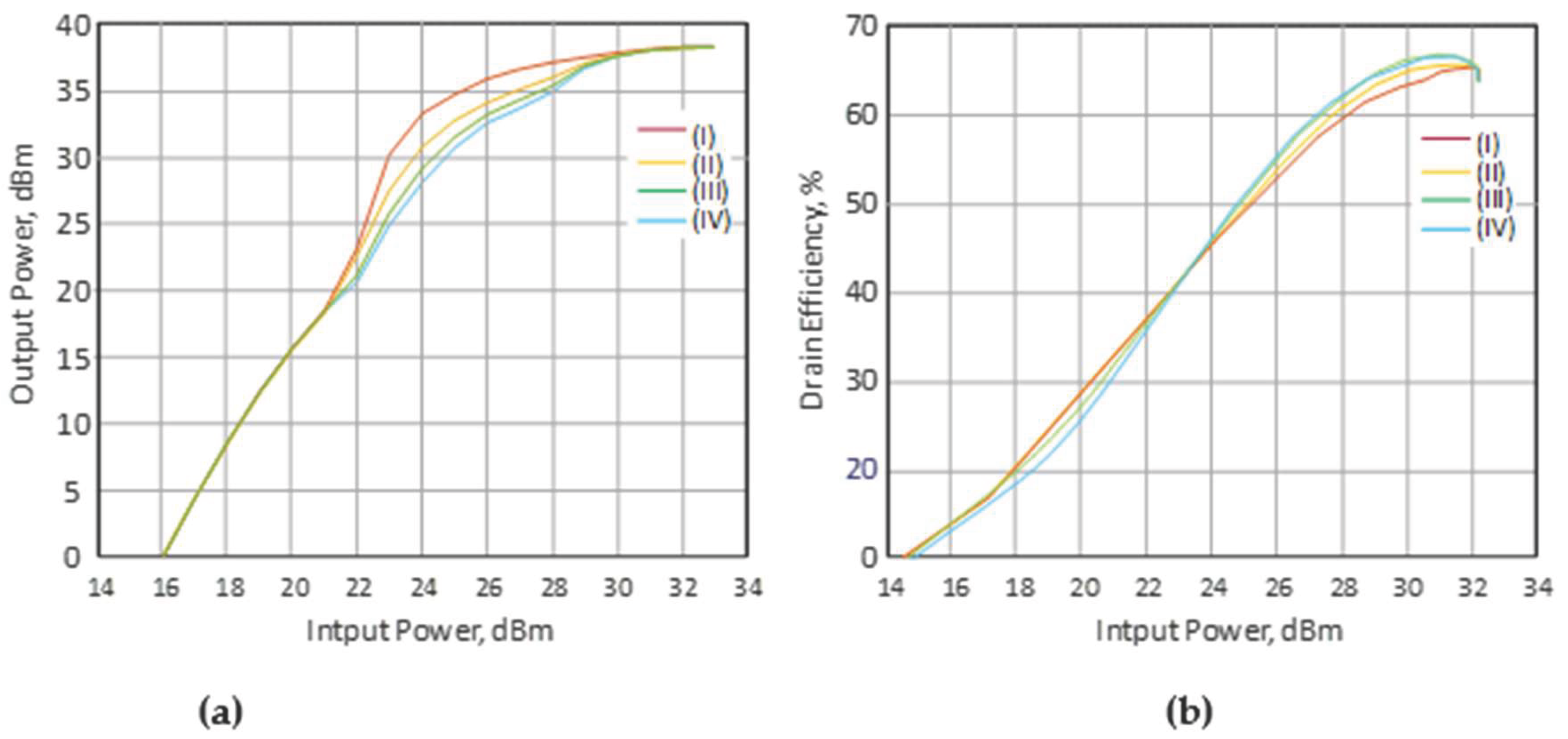
The linearity of the output power response with respect to the input power depends on the slope of the voltage adjustment characteristic. Therefore, different voltage adjustment profiles are studied to demonstrate the influence on the output power response. The measured results of the output power versus the input power at different slopes of the voltage adjustment characteristics are shown in Figure 9(a). In accordance with the presented results, voltage adjustment profile III gives the best result in terms of the linearity of the output power with increasing the input power and improved efficiency. It should be stress that the dependence of efficiency on output power does not change markedly when the slope of the voltage adjustment characteristic of the modulator changes, Figure 9(b). In the case of IV voltage response the efficiency has a more pronounced S-shaped character, in which in small-signal regime the efficiency decreases. Hence, one can expect better linearity characteristics when using proposed PA with modern signals.
5. Conclusions
The design for a 6W power amplifier featuring dynamic load modulation is proposed. A passive ferroelectric-based output matching network was designed to optimize the transistor’s load impedance as the output power varies. The power amplifier was EM simulated using an equivalent circuit model of the ferroelectric capacitor. Parameters of the transistor’s output matching network were evaluated using load-pull techniques to ensure high efficiency during back-off conditions. The load-modulated power amplifier has been fabricated and tested, with measurements indicating that efficiency exceeds 50% at an 8 dB back-off while tuning the output matching network by applying control voltages ranging from 2 to 16V. Additionally, the control bias modulator to adjust the voltage applied to the capacitor based on the input signal power was developed. Experimental studies of the designed power amplifier using the bias modulator aimed to maximize efficiency during back-off. Results demonstrate a 20% improvement in efficiency with dynamic load modulation at 8 dB back-off, and it was shown that the linearity of the output power is influenced by the slope of the voltage adjustment characteristic of the bias modulator. It should be noted, the DLM is of practical interest as a single PA stage, but also the main amplifier stages in Doherty or LMBA structure can be supplemented with load modulation techniques based tunable FE-based OMN to improve the efficiency in back-off.
Author Contributions
Conceptualization and supervision, original draft preparation, writing—review and editing, P. Turalchuk; Software, modeling, validation, investigation, data analysis, visualization, I. Filipiuk, B.Iskakov; All authors have read and agreed to the published version of the manuscript.
Funding
This work has been supported by the Russian Science Foundation (Project № 23-29-00927, https://rscf.ru/project/ 23-29-00927).
References
- Ruan X, Wang Y, Jin Q. A review of envelope tracking power supply for mobile communication systems. CPSS Transactions on Power Electronics and Applications. 2017 Dec;2(4):277-91.
- Camarchia, V., Pirola, M., Quaglia, R., Jee, S., Cho, Y. and Kim, B., 2015. The Doherty power amplifier: Review of recent solutions and trends. IEEE Transactions on Microwave Theory and Techniques, 63(2), pp.559-571.B. Kim, J. Kim, I. Kim and J. Cha, “The Doherty power amplifier” IEEE Microw. Mag, vol.7, no.5, pp.42-50, Oct. 2006.
- Grebennikov A, Bulja S. High-efficiency Doherty power amplifiers: Historical aspect and modern trends. Proceedings of the IEEE. 2012 Sep 13;100(12):3190-219.
- Shepphard DJ, Powell J, Cripps SC. An efficient broadband reconfigurable power amplifier using active load modulation. IEEE Microwave and Wireless Components Letters. 2016 May 13;26(6):443-5.
- Quaglia R, Cripps S. A load modulated balanced amplifier for telecom applications. IEEE Transactions on Microwave Theory and Techniques. 2017 Nov 30;66(3):1328-38.
- Raab FH. High-efficiency linear amplification by dynamic load modulation. In IEEE MTT-S International Microwave Symposium Digest, 2003 2003 Jun 8 (Vol. 3, pp. 1717-1720). IEEE.
- Turalchuk PA, Filipyuk IA. Dynamic Load Modulation Power Amplifier Using Tunable Impedance Transformer. In 2023 Radiation and Scattering of Electromagnetic Waves (RSEMW) 2023 Jun 26 (pp. 136-139). IEEE.
- Fu, Jia-Shiang, and Amir Mortazawi. Improving power amplifier efficiency and linearity using a dynamically controlled tunable matching network. IEEE Transactions on Microwave Theory and Techniques 56.12 (2008): 3239-3244.
- Chen K, Peroulis D. Design of adaptive highly efficient GaN power amplifier for octave-bandwidth application and dynamic load modulation. IEEE Transactions on Microwave Theory and Techniques. 2012 Apr 3;60(6):1829-39.
- Nemati HM, Fager C, Gustavsson U, Jos R, Zirath H. Design of varactor-based tunable matching networks for dynamic load modulation of high power amplifiers. IEEE Transactions on Microwave Theory and Techniques. 2009 Apr 14;57(5):1110-8.
- Nemati HM, Cao H, Almgren B, Eriksson T, Fager C. Design of highly efficient load modulation transmitter for wideband cellular applications. IEEE transactions on microwave theory and techniques. 2010 Oct 7;58(11):2820-8.
- Andersson CM, Gustafsson D, Yamanaka K, Kuwata E, Otsuka H, Nakayama M, Hirano Y, Angelov I, Fager C, Rorsman N. Theory and design of class-J power amplifiers with dynamic load modulation. IEEE transactions on microwave theory and techniques. 2012 Oct 23;60(12): 3778-86.
- Bengtsson O, Maune H, Gölden F, Chevtchenko S, Sazegar M, Kurpas P, Wiens A, Jakoby R, Heinrich W. Discrete tunable RF-power GaN-BST transistors. In 2012 42nd European Microwave Conference 2012 Oct 29 (pp. 703-706). IEEE.
- Preis S, Kienemund D, Wolff N, Maune H, Jakoby R, Heinrich W, Bengtsson O. Thick-film MIM BST varactors for GaN power amplifiers with discrete dynamic load modulation. In 2017 IEEE MTT-S International Microwave Symposium (IMS) 2017 Jun 4 (pp. 281-284). IEEE.
- Turalchuk, P. A., et al. Highly efficient X-range AlGaN/GaN power amplifier. Technical Physics Letters 43 (2017): 787-789.
- Fu JS, Mortazawi A. Improving power amplifier efficiency and linearity using a dynamically controlled tunable matching network. IEEE Transactions on Microwave Theory and Techniques. 2008 Nov 18;56(12):3239-44.
- Cao H, Nemati HM, Tehrani AS, Eriksson T, Grahn J, Fager C. Linearization of efficiency-optimized dynamic load modulation transmitter architectures. IEEE Transactions on Microwave Theory and Techniques. 2010 Mar 25;58(4):873-81.
Figure 1.
The scheme for Dynamic Load Modulation Power Amplifier based on Ferroelectric Tunable Matching Network.
Figure 1.
The scheme for Dynamic Load Modulation Power Amplifier based on Ferroelectric Tunable Matching Network.
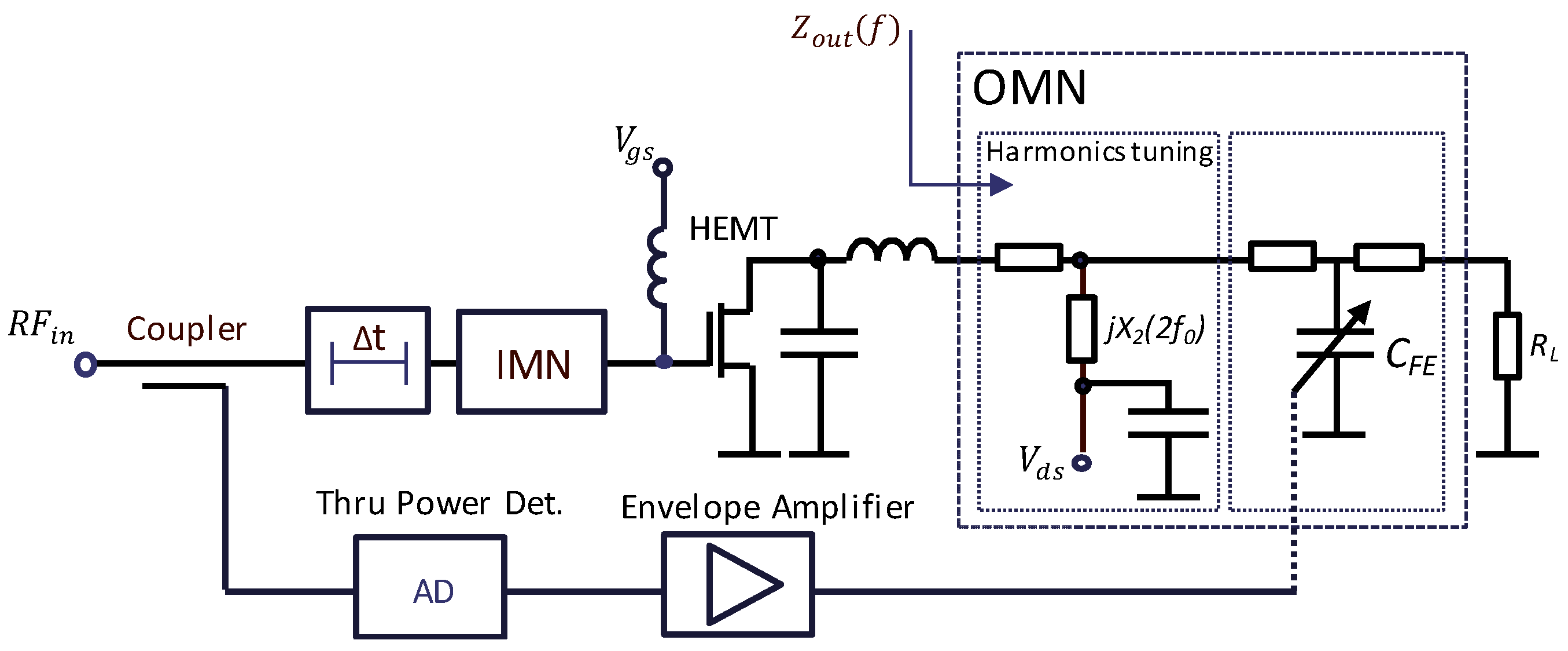
Figure 2.
The results of load-pull for GaN HEMT transistor at 2.5 GHz central frequency. The dashed line - the impedance Zout provided by tunable OMN with changing CFE in range of 0.8 – 2.35pF.
Figure 2.
The results of load-pull for GaN HEMT transistor at 2.5 GHz central frequency. The dashed line - the impedance Zout provided by tunable OMN with changing CFE in range of 0.8 – 2.35pF.
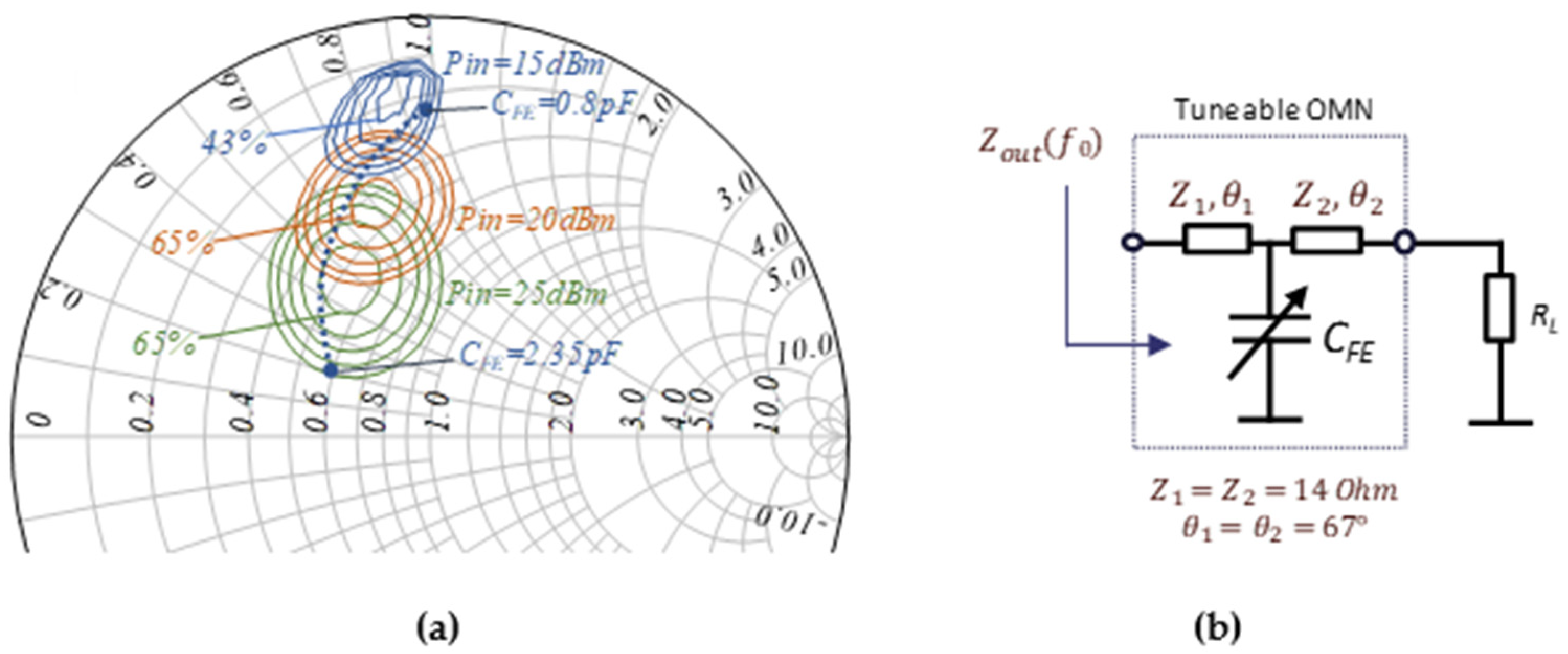
Figure 3.
(a) The modeling and measurement results of the frequency dependence of the FE capacitance for different applied voltages; (b) Measurement of the FE capacitance as a function of applied voltage at 2.5 GHz compared with modeling results.
Figure 3.
(a) The modeling and measurement results of the frequency dependence of the FE capacitance for different applied voltages; (b) Measurement of the FE capacitance as a function of applied voltage at 2.5 GHz compared with modeling results.
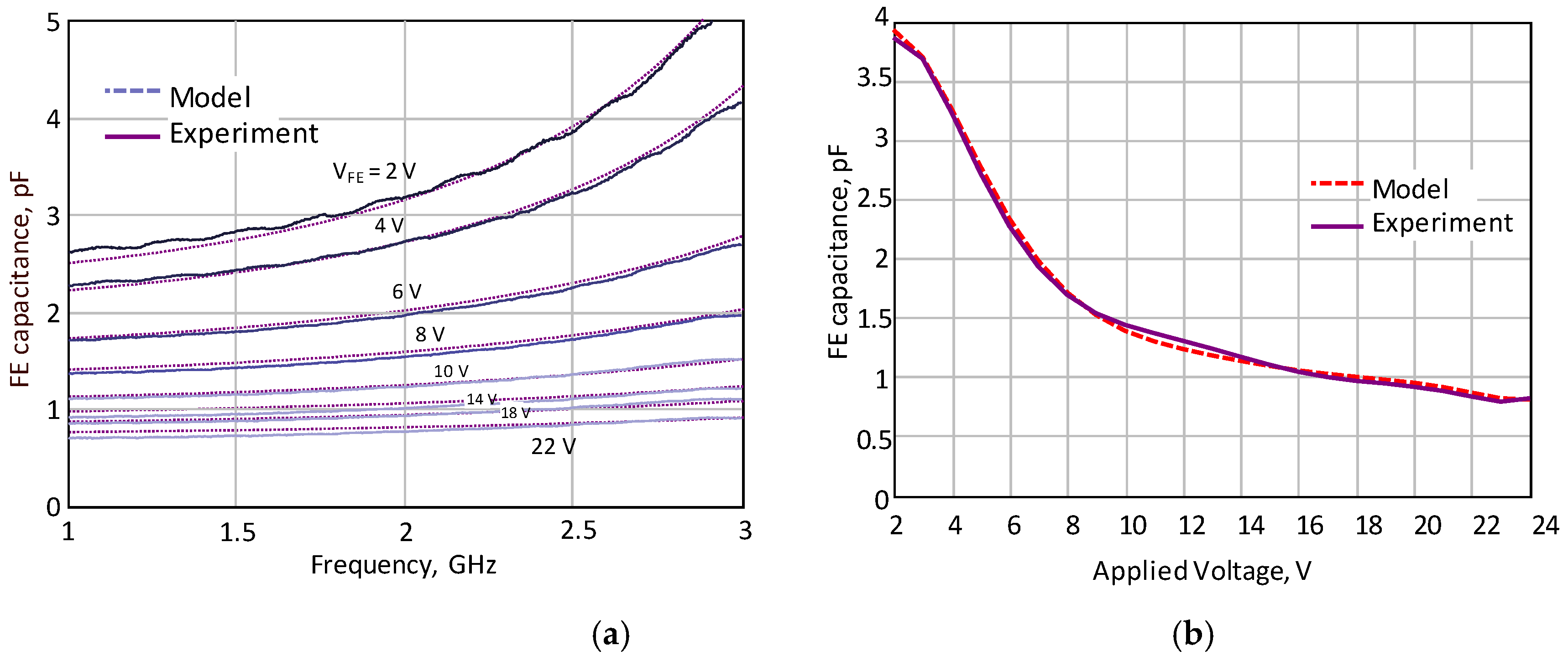
Figure 4.
FE IC equivalent circuit with the extracted parameters.
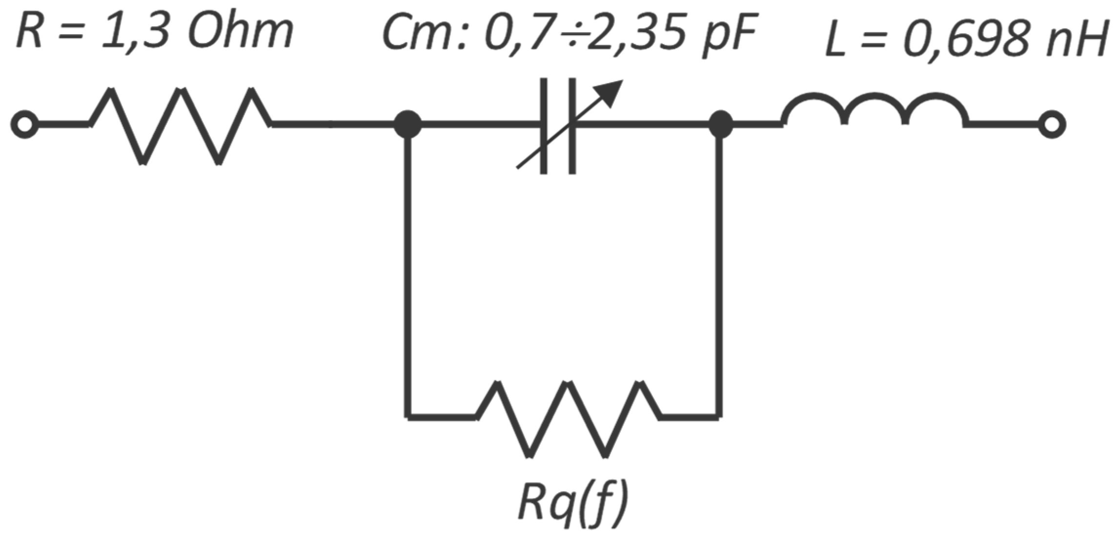
Figure 5.
(a) The design of the PA with ferroelectric based OMN;(b) modeling results of the power added efficiency as a function of the output power for different values of the CFE (1.6 pF – 0.7pF).
Figure 5.
(a) The design of the PA with ferroelectric based OMN;(b) modeling results of the power added efficiency as a function of the output power for different values of the CFE (1.6 pF – 0.7pF).
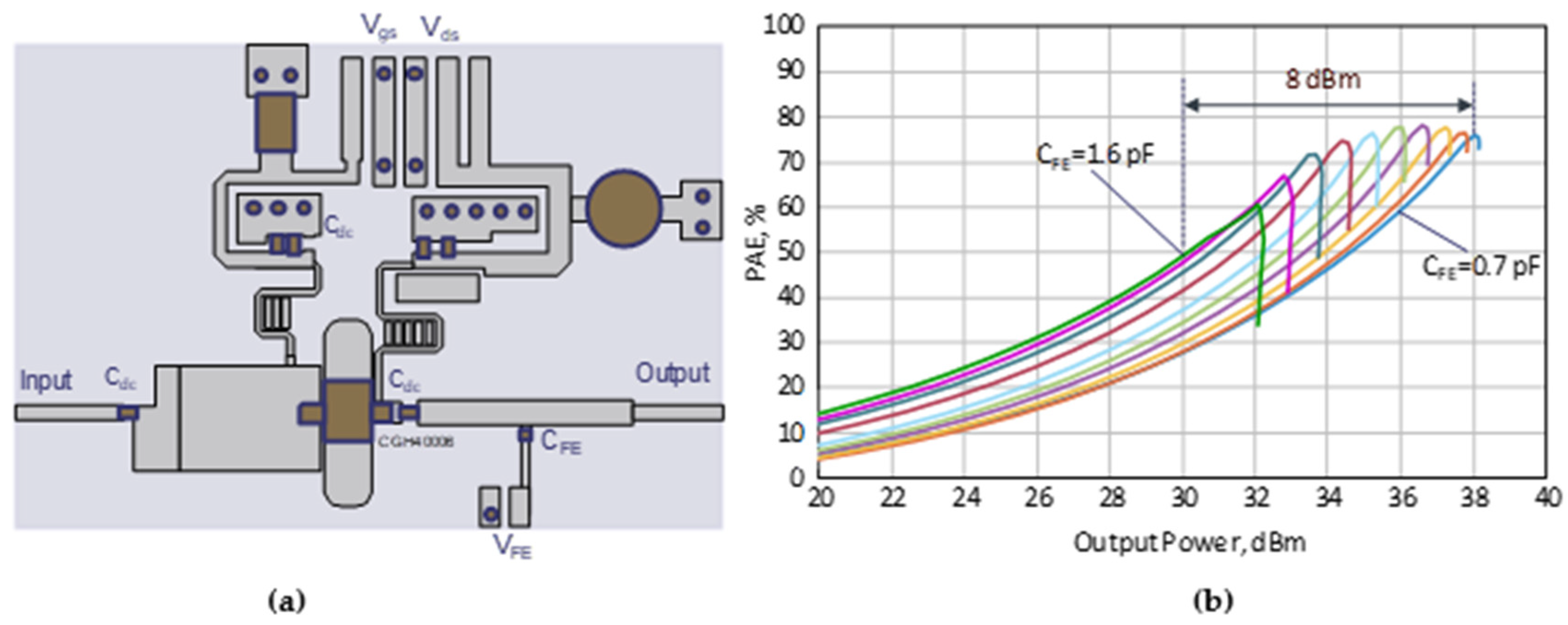
Figure 6.
(a) Fabricated load modulated PA with ferroelectric based OMN; (b) Measured drain efficiency versus the output power for different values of the applied voltage to the FE capacitor.
Figure 6.
(a) Fabricated load modulated PA with ferroelectric based OMN; (b) Measured drain efficiency versus the output power for different values of the applied voltage to the FE capacitor.
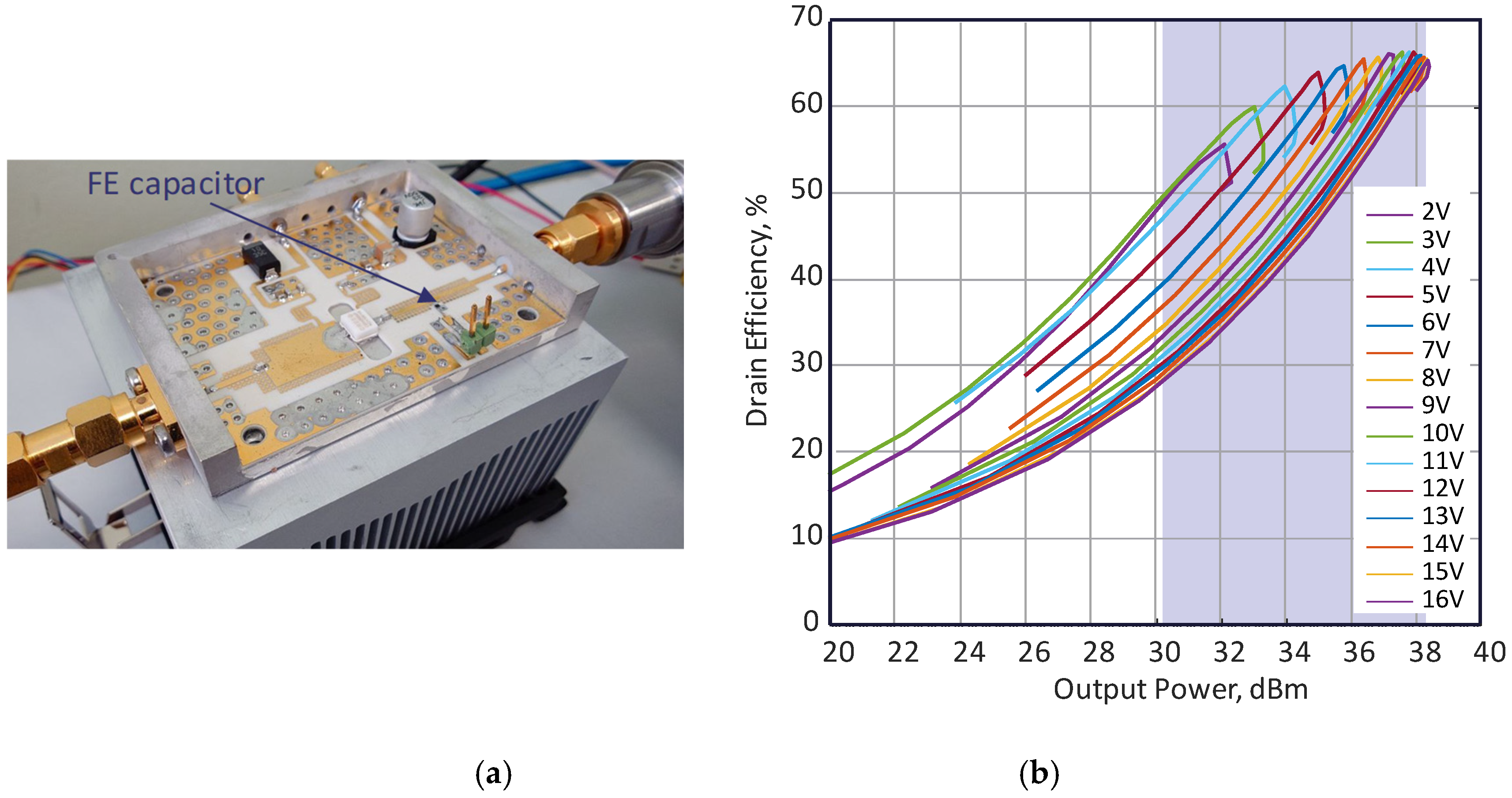
Figure 7.
(a) Scheme for the bias modulator; (b) output voltage adjustment characteristics of the bias modulator as a function of the input power.
Figure 7.
(a) Scheme for the bias modulator; (b) output voltage adjustment characteristics of the bias modulator as a function of the input power.
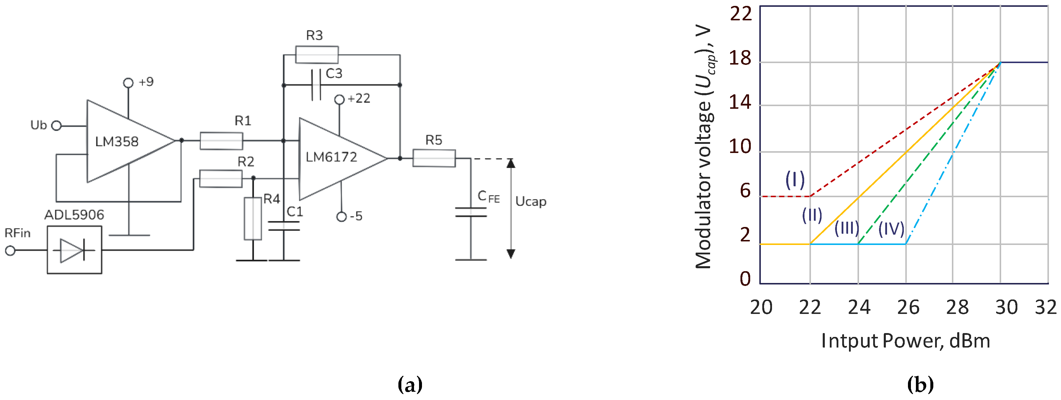
Figure 8.
Measured drain efficiency versus the output power of the DLM PA with bias modulator.
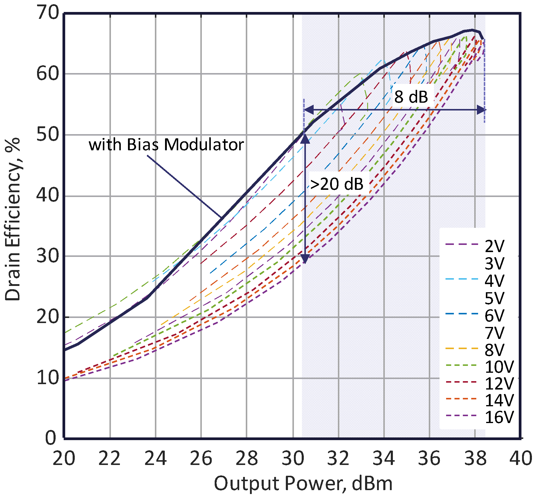
Figure 9.
(a) Measured output power of the DLM PA as a function of the input power for different voltage adjustment responses; (b) measured efficiency of the DLM PA versus the input power for different voltage adjustment profiles.
Figure 9.
(a) Measured output power of the DLM PA as a function of the input power for different voltage adjustment responses; (b) measured efficiency of the DLM PA versus the input power for different voltage adjustment profiles.
Disclaimer/Publisher’s Note: The statements, opinions and data contained in all publications are solely those of the individual author(s) and contributor(s) and not of MDPI and/or the editor(s). MDPI and/or the editor(s) disclaim responsibility for any injury to people or property resulting from any ideas, methods, instructions or products referred to in the content. |
© 2024 by the authors. Licensee MDPI, Basel, Switzerland. This article is an open access article distributed under the terms and conditions of the Creative Commons Attribution (CC BY) license (https://creativecommons.org/licenses/by/4.0/).
Copyright: This open access article is published under a Creative Commons CC BY 4.0 license, which permit the free download, distribution, and reuse, provided that the author and preprint are cited in any reuse.


