Submitted:
19 September 2024
Posted:
23 September 2024
You are already at the latest version
Abstract
Halide perovskite are known by their (1) organic inorganic hybrid and (2) inorganic halide perovskite. Having this in mind, monolithic perovskite/silicon tandem solar cell has already demonstrated extraordinarily high performance in the field of photovoltaic with current efficiency of 29.15%, breaking the efficiency limit for silicon solar cell. Currently, halide perovskites become successful not only in photovoltaic but also in many other related potential optoelectronic applications. Because of this reason, the origin of their multifunctional properties, remarkable energy harvesting and emitting efficiency and the corresponding potential applications in various optoelectronic devices become controversial issues and hot topics of academic research this time. In this review, nano-engineering strategies, microscopic origins and mechanisms are reviewed well to make clarity on what the origin of multifunctional properties such as tunability, ferroelasticity, piezoelectricity, pyroelectricity and thermoelectric properties of halide perovskites. Moreover, the coexistence of multiple properties makes halide provskites possible for synergistic applications and multifunctional perspectives such as emerging energy harvesting, conversion technologies, nano-plasmonic sensing and electromechanical applications, which are now open for the scientific community for further detail investigations. To successfully explore this field, advanced nanometer scale domain characterization tools are highly relevant to understand the microscopic origin of these electrical properties; aid the commercial enterprises and the research institutions. Not only the microscopic origin but also identifying factors and issues affecting the successful understanding and presence or absence of these electrical parameters should be primary task in this review. Finally, the big challenges for operation of halide perovskites owing to temperature, moisture, light, air, etc. induced material degradation and device deteriorations as well as lattice instability, nano scale defects, surface and bulk defects should be considered while dealing with these future research topics.
Keywords:
nano-engineering
; microscopic origin
; strain
; energy harvesting
; photo-sensing
; Nano-plasmonic sensing
; photoflexoelectricity
; halide perovskites
Broader context
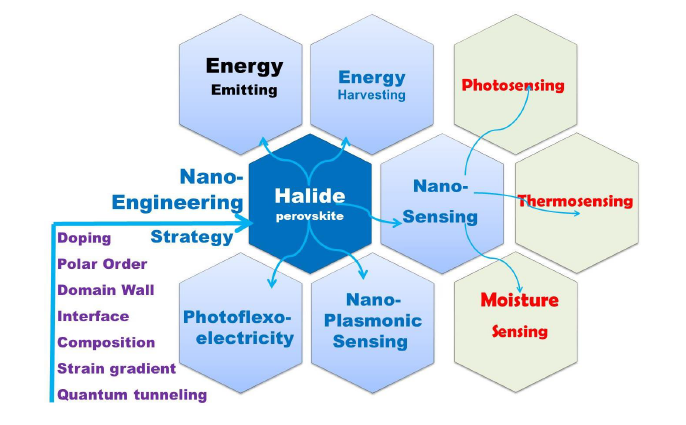
Nano-engineering halide peroveskite towards energy harvesting, nanosensing and photoflexoelectricity beyond photovoltaic and energy emitting applications become great scientific and technological areas of revolution in this era. In this nano-engineering perspective of halide perovskites, understanding the microscopic origins and mechanisms of potential multifunctional properties are highly required for the broader context of halide perovskites. Moreover, the characterization methods of understanding and the big challenges for operation of halide perovskites during practical applications have vital role in the development of new potential revolutions.
1. Background
Perovskites materials are two types in nature: oxide and halide perovskites or chalcogenides and organic perovskites. Likewise, halide perovskite semiconducting materials are of two types: organic inorganic hybrid halide and inorganic halide perovskites. Halid perovskite based solar cells demonstrated extraordinarily superior performance in the area of photovoltaic (29.15%).[1,2] This record breaks the theoretical limit for silicon solar cell.[3,4] They show high absorption coefficient (~105 cm−1),[5,6] low exciton binding energy, and low non-radiative charge-carrier recombination, all reflected in the sharp absorption onset and small Urbach energy.[5] High power-conversion efficiencies using MAPbI3 have been achieved in both mesoporous structures and planar heterojunction structure devices. In addition to the photovoltaic functionalities, the organic inorganic hybrid halide (OIHH)perovskite, containing of ABX3 (A organic monovalent cation, B divalent metal, X anion, could act as a potential platform for the optimization and design of materials with preferred application[7] for wide range energy applications such as electronic devices, photocatalytic and catalytic processes beyond the photovoltaic.
However, the secret and origin of their semiconducting properties, remarkable performance and wide range potential applications are not yet successfully discovered. Numerous opinions have been reported to clarify the outstanding solar cell performance, together with the high VOC/EG ratio. A high VOC indicates low charge recombination and, in fact, solar cells with appreciably low recombination can be prepared with (OIHH) perovskite materials.[8] Theoretically, these materials were considered as polar,[9,10] as were confirmed by the experimental observations of the piezoelectricity[11,12,13,14,15] and ferroelasticity[16] for MAPbI3 materials. Later, such semiconductor materials are proven to be polar and nonpolar depending on the environment, composition and processing.[17] Moreover, photo induced enrichment in the piezoelectric coefficient d33[10,11] and photostriction effect[18] in these materials propose a powerful relation between the optical response and their polar nature. A much discussed suggestion to justify for the better performance engages the presence of arbitrarily oriented ferroelectric domains. Furthermore, ferroelectricity has been suggested as a potential explanation for the increasing charge carrier lifetimes and low charge recombination rates,[19,20] resulting in efficient charge separation.[21] Besides, it was suggested that the hysteresis behavior observed in the I-V (current-voltage) of OIHH perovskite cells was considered because of ferroelectric behavior[9] but later it is confirmed that this hysteresis is because of intrinsic ion migration or ionic transport.[22,23] Moreover, it has also been of high technological interest to explore the piezoelectric properties of the hybrid perovskites for applications such as piezoelectric generators or energy harvesting devices.[14,15] The ability to control and manipulate the polar properties in these materials thus has important implications in gaining enhanced understanding of its photovoltaic response and wide range potential applications. Hence, the aim of this review article is to comprehensively review the recent information about nano-engineering strategies such as strain and doping, polar order and domain wall engineering, and interface and composition engineering strategies, microscopic origin and mechanisms of multifunctional properties, nano-scale domain nano-characterization approaches as well as their wide range functionalities and applications such as energy harvesting, nano-plasmonic sensing, electromechanical applications and big challenges of halide perovskites practical operation. Its objective is also to shed light on what the origin of remarkably multifunctional properties, energy harvesting, nanosensing and electromechanical applications beyond high photovoltaic efficiency of these highly relevant materials. Furthermore, the scope of this article is starting from the idea of possible material nano-engineering strategies with the intention on how to design new material with its new property to enlighten the current scientific journey and make the scientific community become more alert towards four important points: 1) whether halide perovskites own all these multifunctional properties or not; 2) whether the remarkable energy harvesting, conversion, emitting and sensing efficiency are really originated from those relevant electrical multifunctional properties or not; 3) whether these materials are to this extent highly applicable and relevant in wide range research fields integrating the physical and chemical science with engineering and biological applications or not. 4) Whether nano-engineering strategy boost the performance of halide perovskite in wide range applications or not. The researchers hope that this review will be useful for new paradigm shift in research, academia and enterprise in doing new breakthroughs for the development of halide perovskite industry and education.
2. Nano-Engineering Strategy of Designing New Property
Can Nano-Engineering Make Halide Perovskite Revolutionize New Application Paradigm Shift?
Owing to growing desires of clean and renewable solar energy, researchers are constantly investigating novel materials and basically investigating photoelectric conversion mechanisms for the better performance of photovoltaic devices.[24,25] Furthermore, the photovoltaic effect is employed to straightforwardly collect solar energy by changing the incident photons into flowing free charge carriers and thus create electricity. In general, the ferroelectric photovoltaic effect[26,27,28,29,30,31] initiates from the spontaneous electric polarization in ferroelectric materials.[32,33] A sole feature of ferroelectric-photovoltaic devices is that the photocurrent direction can be switched by altering the spontaneous polarization way of ferroelectrics with the electric field. Importantly, there are two vital processes that verify the photovoltaic effect: 1) the electrical-charge carries such as electron-hole pairs are generated by absorbing photons in active layers of the devices, i.e. semiconductors, dyes.[34,35] 2) the photo-produced electron-hole pairs are concurrently detached by a built-in asymmetry potential made in p-n/Schottky junction[36] or two electrodes with dissimilar work functions.[37,38] Furthermore, photovoltaic devices derived from ferroelectric properties have drawn important concentration due to lots of sole compensation, for example the switchable photocurrent and photovoltage above band gap open circuit voltages.[39] Moreover, the photovoltaic effect in polar materials has drawn considerable attention, since the photoconversion mechanism can be developed for the expansion of superior photovoltaic devices that produce a high voltage. Nevertheless, the voltage that can be generated by present semiconductor-based devices is of the order of a few volts at most. Recently, it has been reported that high voltages can be produced in ferroelectric thin films,[40,41] which has encouraged energetic research and expansion of photoelectric conversion devices by means of ferroelectric materials. However, numerous confronts left unsolved, for example complexity in launching device blueprint and still unknown principles yet discovered following power generation. In representative semiconductor solar cells, the photo-generated electron-hole pairs are separated by the built-in field in the pn junction, and the photovoltage is bounded by the band gap. Nevertheless, with the absence of inversion symmetry in polar materials, photocurrents can be produced beneath the consistent illumination because of noncentrosymmetry in their crystal structures, which is named bulk photovoltaic effect.[42,43]
Such ferroelectrics additionally demonstrate anomalous photovoltaic effect that the photovoltage can reach numerous tens of thousands of volts, more than the band gap.[43,44,45] Halide perovskite materials have been proposed as pyroelectric, piezoelectric, ferroelectric materials for multifunctional energy harvesting beyond photovoltaic applications. However, the energy harvesting properties and applications, and the engineering strategies to enhance these multifunctional properties are not well developed. Therefore, in this section, energy harvesting multifunctional engineering materials strategy such as strain engineering, doping engineering, polar order engineering and domain wall engineering are well organized as performance enhancement approaches and strategies.
2.1. Strain and Doping Engineering Approach
In addition to band gap engineering,[46,47,48] strain and doping engineering has been broadly applied in the semiconductor industry to achieve fast transistors with both compressive and tensile strain. Moreover, in order to enhance the ferroelectric, piezoelectric and pyroelectric properties of halide perovskites, two nanoengineering approaches i.e., strain engineering[49,50,51] and doping engineering[51] have been proposed.
2.1.1. Strain Engineering
Strain engineering, determined by relaxation mechanisms, interface and lattice mismatch,[52] is considered as modulator of broad multifunctional properties and electronic structures for wide range applications[53,54] and thus it is useful strategy to improve the research field of halide perovskites. The MA flip rotation is powerfully connected to cell aspect ratio (c = a) of MAPbI3. It also becomes energetically less likely when c = a bigger, indicating a bigger energy disparity between ferroelectric state (this energy disparity is described as ΔEAFE-FE) and anti-ferroelectric state. According to this result, one may anticipate that a compressive uniaxial or biaxial strain can expand c=a of tetragonal MAPbI3[55,56] and increase the FE state's energetic benefit above the AFE states. In order to realize it, it was calculated ΔEAFE-FE and c=a with respect to biaxial and uniaxial strain from -3% to +3%, with negative (positive) values described as compressive (tensile) strain[51] and found compressive biaxial or uniaxial strain increases the energetic benefit of the FE state over the AFE states, while tensile strain reduces it. Therefore, strain engineering is an option to increase the trend of ferroelectric dipole ordering in tetragonal MAPbI3.[57]
It has been reported that the strain is induced by mismatched thermal expansion between the films and the substrates.[58] Hence, it has also been suggested that halide perovskite films prepared by presented techniques are strained during the thermal annealing process.[58] These polycrystalline films have compressive strain in the in-plane and tensile strain out-of-plane direction as shown in Figure 1.
Furthermore, Figure 1A shows there is a peak (110) shift towards lower diffraction angle, indicating that there is presence of lattice strain. Figure 2B shows that the (110) in-plane peak shifts to a lower angle as compared to the strain-free peak of the single crystals, showing a tensile strain in the horizontal direction for the polycrystalline MAPbI3 film. As shown in Figure 1C, the spacing of crystal planes perpendicular to the substrate is measured by the out-of-plane XRD. XRD peak shift from lower to higher diffraction angle, which belongs to smaller plane spacing, as a result, the strain is compressive in the normal direction of the films. The in-plane XRD to measure spacing is shown in Figure 1D, which belongs to the larger plane spacing, as a result the strain is tensile strain as shown in Figure 1B.
Moreover, strain engineering is useful mechanism for engineering strain sensitive energy harvesting devices such as piezoelectric pressure/strain sensors, photodetectors and nanogenerators.[59,60,61] This practical approach is essential to monitoring the optoelectronic and electronic properties of piezoelectric inorganic materials through the application of working internal or external stress. This time there become various energy harvesting devices fabricated using halide peroveskite materials. Thus, strain engineering is useful to develop halide peroveskite piezoelectric pressure/strain sensors, photodetectors and nanogenerators as well as to solve stability issues. Materials with mobile ions are responsible to introduce stress and hence halide perovskites have ions showing mobility upon which strain can change activation energy of these migrating ions.[62] Thus, extensive analysis and understanding of strain is required to improve energy harvesting halide peroveskite performance.[63] But, strain formation at the interface is observed reducing the device performance of solar cells and hence careful attention shall be given not only for its usefulness but also for its side impact that may cause device failure.[64]
2.1.2. Doping Engineering
Moreover, doping engineering is an enabler for achieving better performer and stable devices such as fabrication of piezoelectric energy harvester.[65] This can be done via targeted doping.[66,67] In this case, it is vital to understand the effect of dopant structure[68] during nanoengineering to monitor nanostructure based devices in improving their performance in various applications such as nanostructured thermoelectric.[69] Furthermore, the elastic and piezoelectric properties are highly important for energy harvesting devices. Thus, optimizing both properties at the same time is quite difficult but essentially required. This difficulty can be solved via doping engineering.[70] For instance Seebeck coefficient is observed increasing through the application of electrochemical doping in thermoelectric conductive polymers.[71] Besides, doping is useful to halide perovskites for the purpose of band alignment, enhanced charge transfer thereby increasing performance. But, the effect of higher doping has an impact of increasing recombination and reducing charge carrier density and mobility thereby reducing power conversion efficiency.[72] Hence researchers shall consider not only its usefulness but also its side effect of device deteriorations. Doping strategies are reported elsewhere[73] to increase performance of photovoltaic devices and shall be followed to unleash the potential of halide perovskites[74] for the fabrication of energy harvesting devices. This is not only to achieve energy harvesting materials but also single-phase materials suitable for emission as can be seen in [(CH3)3S]2SnCl6·H2O crystals.[75]
Besides strain engineering, it has been proposed as alternative to improve ferroelectric dipole ordering in the course of doping engineering,[51] specifically, to replace I with smaller halogen anions, like Br or Cl. This proposition is rooted in the idea that substitution doping with smaller ions uses natural compressive strain on unit cells.[76,77] In addition, doping can also encourage lattice strains that are less likely in the course of the function of external forces.[78] That is, I sites in tetragonal MAPbI3 are either on the MAI layers or PbI2 layers. For example, the doping on the MAI layers shortens Pb-halogen bonds along the c axis, and decreases the c lattice parameter; while doping of Br (Cl) on the PbI2 layers shortens Pb-halogen bonds in the ab-plane, and decreases the a and b lattice parameters. So as to add to c=a, the ideal doping should not be on the MAI layers rather it is better if it is on the PbI2 layers.[51] For instance, Br doping on the PbI2 layers is energetically preferred to that on the MAI layers by 16 meV per unit cell owing to the presence of eight I anions on the PbI2 layers per unit cell while four on the MAI layers.[51] This indicates that there is higher probability for doping to substitute iodine on PbI2 compared to MAI. The higher amount of dopant, such as Br or Cl, gets more space on the doping site where there is higher amount of substance to be replaced or substituted, i.e. PbI2 in this case.
2.2. Polar Order and Domain Wall Engineering Approach
With the perspective of enhancing energy harvesting performance, understanding the mechanisms and polar order and domain engineering play a vital role. While the polar order engineering could be at the A site or B site in the ABX3 3D structure, the domain engineering could be at the surface, wall and interface for heterostructure architectures such as CH3NH3PbI3/PZT. The important mechanism of ferroelelctric phase transition involves order-disorder, displacive type and mixed order-disorder.[79,80,81,82] Moreover, energy harvesting performance can be enhanced using various strategies. Engineering materials strategy mainly stress induced domain wall motion,[83] domain wall switching,[84] depolarization mechanisms, domain wall propagation, stable domain pattern with suitable properties,[85] etc. are useful in developing energy harvester for various applications. In case of halide perovskites, polar order and domain wall engineering are used to some extent but showing
2.2.1. Polar Order Engineering
MAPbI3 perovskites is reported as both polar and nonpolar material.[17,86,87] Because of this reason, polar order engineering is essential in the field of halide perovskites to investigate the polar order and the effect of the presence of this polarity or the absence of this polarity. In spite of the microscopic model, polar order is considered to recline at the center of the ferroelectric photovoltaic effect. Additionally, it is well known that interactions between lattice, orbital order, and polarization parameters in ferroelectric materials show the way to improvement of their physical properties near phase boundaries. One notable example is the huge electromechanical response resulting from phase and polar instability at the morphotropic phase boundaries in relaxor ferroelectrics.[88] On the other hand, polar instability would affect the ferroelectric photovoltaic effect, but, remains mainly unidentified. Therefore, modification of the polar order in a prototypical ferroelectric photovoltaic material at either A-site or B site substitutions would lead to polar order engineering. In this case, understanding the photovoltaic enhancement for compositions near the boundary between the polar and nonpolar phases should get attentions, especially for halide perovskite materials. Thus, chemical substitution leads to a direct-indirect bandgap transition and as a result a longer carrier lifetime, conclusions that are supported by theoretical calculations.[28]
2.2.2. Interface and Domain Order Engineering
The atomic-scale growth practices of heterostructures interfaced materials offer a wealth of fine potential for making novel states at their interfaces,[89,90,91] directing to a huge number of developing physical phenomena and applications as a result of the multifaceted interaction of spin, charge, orbital and lattice degrees of freedom.[92,93,94] Furthermore, in ferroelectric materials, interfaces participate an essential function in the formation of a variety of domain structures.[95] Moreover, the existence of switchable ferroelectric domains in β-CH3NH3PbI3 has been confirmed in recent times via piezoresponse force microscopy.[96] However, the local structure and the electronic properties of domain walls in halide perovskites continue unidentified. In recent times, it has been discovered the energies and electronic structures of 180 and 90° domain walls in MAPbX3 via DFT.[97] Thus, both types of domain walls can be charged or uncharged, depending on the orientation order of the organic molecules around the domain boundaries.[97] Owing to the interaction between strain, depolarization field and gradient energies, topological ferroelectric vortices can be produced in heterostructure structure super lattices. Fascinatingly, the domain structures can be engineered, for instance, from a1/a2 domains to vortex–antivortex structures and then to classical flux-closure domain structures with the raise of the super lattice period, strongly depending on the interface effects of the depolarization field.[98] Intriguingly, this approach to enhance photovoltaic effect in halide perovskite materials is not yet touched and needs more to investigate and engineer the domain at the wall and interface. Moreover, upcoming investigations on the interface structure and its effect on switching or the inclusion of additional electrostatic contributions, for instance, depolarizing fields from finite screening, flexoelectric effects, and inhomogeneous space charges are open to the society.
The purpose of ferroelectric domains formation is reducing the electrostatic energy of the depolarizing fields and the elastic energy associated with the mechanical constraints to which the ferroelectric material is subjected as it is cooled through the paraelectric-ferroelectric phase transition.[99] Furthermore, the surface charge induced at the onset of the spontaneous polarization with nonhomogeneous distribution and at the transition temperature generates an electric field named as the depolarizing field Ed, oriented in contrast to PS (Scheme 6). The two important minimizing mechanisms of electrostatic energy correlated with the depolarizing field is either: (1) the splitting of a ferroelectric into domains with awkwardly oriented polarization, Scheme 9, or (2) the compensating of a depolarizing charge by electrical conduction or by charges from the nearby substance. (3) Ferroelectric split in crystal into domains may also take place because of the persuade of mechanical stresses, as shown in Scheme 5.[99,100] Essentially, there are two types of twinning in accordance with the direction of the polar axis between neighboring twined domains in the tetragonal perovskite: perpendicular (90◦ domain) or antiparallel (180◦ domain)[101] as shown in Scheme 3. Thus, a 180° phase-contrast or charged domain wall has been shown in the β-MAPbI3 thin films[102] and generate high electric field that induces free charge buildup across the wall and piercingly amplify the domain-wall conductivity.
2.3. Composition Engineering Strategy
Important classes of materials are revolutionizing the energy harvesting research field as recent developments already indicated.[103,104,105] Such materials are named as organic inorganic hybrid perovskites. The oxide perovskites are in completion with such new molecular ferroelectric materials in this field. Such materials are summarized by Qiong Ye and Ren-Gen Xiong research group.[106] Their advantage of ease of low cost, solution processing, homochirality, biocompatibility, environmental friendliness, a tunable chemical structure, as well as good ferroelectricity, piezoelectricity deal make halide perovskites encouraging for the future of high-performance.[107] A precise molecular design has been suggested to engineer energy harvesting molecular perovskite families.[108] This molecular design depends on the interaction of organic-inorganic cage,[109] role of chemical substitution at both organic and inorganic cages,[78,110,111,112] role of polar phonon interaction,[113,114] composition (or mixing) the chemicals using ratio of atoms,[115,116,117,118,119,120] polar order and domain wall,[101,121,122,123] chirality of organic cations,[124] spin-orbit Coupling,[125] hydrogen bonding,[126] cation ordering,[127,128,129,130,131] doping effect,[132] quantum and dielectric confinement.[133] Confinement engineering has also been reported to design 2D lead halide hybrid perovskite ferroelectrics.[134] Materials with multifunctional properties are greatly required to develop multifunctional devices upon introducing to various external stimuli. Such multiferroics is due to the coexistence of two or more properties in a single material such as magnetism and ferroelectricity, switchable dielectric and thermochromic luminescence properties as well as photovoltaic and optoelectronic properties observed in the hybrid halide perovskites.[135,136] But, the coexistence of multiple properties in halide perovskites is not yet known whether such multiple properties are mutually inclusive or exclusive. Ferromagnetism and ferroelectrics are mutually exclusive because ferroelectrics needs empty d orbital while ferromagnetism requires full d orbital. Moreover, feroelectricity/superconductivity/polarity coexistence is not yet discovered. Thus, ferroelectric property in halide perovskites is composition dependent as summarized in Table 1.
3. Microscopic Mechanisms and Origins of New Property
To develop high performance energy harvesting halide perovskites devices, understanding of both macroscopic and microscopic properties of these materials is highly required. Parameters such as pressure, texture, colour, volume, density, and temperature are considered as macroscopic properties while quantum states, atomic mass, electron spin, molecular bond lengths, and bond energies, of individual particles are considered as microscopic properties. The macroscopic properties of halide perovskites are entirely studied[160] while the microscopic properties are not well studied yet. For this purpose, this section is mainly focusing on discussing the microscopic properties of halide perovskites. This will help researchers to have clarity on these microscopic properties while developing new energy harvesting and emitting devices. An interesting advantage of halide perovskite materials is their low cost solution based synthesis method,[161] exceptional quantum yields coupled with structural and compositional tunability.[162] Halide perovskites are easy to synthesize them but difficult to handle. This is because of their degradation and unstable property when exposed to oxygen and moisture.[160,163,164] irrespective of these problems halide perovskites have promising wide range energy harvesting and emitting applications. What could be the origin of these wide range potential energy harvesting, photosensing and nano-sensing applications? To elaborate this big question, understanding the microscopic origins and mechanisms of multifunctional properties is a vital way that can’t be ignored. This is the big issue we want to present for the betterment of the current energy harvesting multifunctional properties of halide perovskites (scheme 4).
Energy harvesting piezoelectric materials would be safe if they are non-toxic, stable, acceptable cure temperature and easy poling treatments for the reasons of practical applications. Efforts such as looking for materials that have non-toxic, stable, high cure temperature and easy poling treatments have been made.[165] Energy harvesting halide perovskites are facing practical applications because of toxicity, instability, bias-induced material degradation[166] and unexpected inconsistency in forward–backward I–V characteristics.[167] But, some reports indicated that halide perovskites don’t face low cure temperature and difficulties in poling treatment owing to their switchable spontaneous electric polarization.[168] Furthermore, ionic diffusion contribution has been detected causing increased radiative recombination.[167]
From the view point of discovering new energy harvesting material, materials with large proof mass displacement, high strain and tolerant to high strain are required.[169] Thus, materials that are not fragile but have high elasticity property are more attractive for piezoelectric energy harvesting. For instance, polyvinylidene fluoride (PVDF) fulfills such requirement. All these requirements are to maximize energy transduction. On the other hand, thermoelectric energy harvesting requires low thermal conductivity K, high Seebeck coefficient α and high electrical conductivity.[169] For this purpose, low phonon materials and scalable fabrication methods are required.[170] Not only piezoelectric and thermoelectric effects but also pyroelectric effect is important for energy harvesting. In pyroelectric energy harvesting both temperatures change in time and polar point symmetry are required points every researcher shall know. As it is green energy source, energy harvesting materials need to have piezoelectric, thermoelectric and pyroelectric properties based up on which energy is collected to fulfill human energy demand. Furthermore, to enhance the efficiency of harvesting the quality factor would be required. The higher quality factor the lower heat lost and less damping in energy conversion boosting efficiency of the energy harvester.
Scheme 4.
Microscopic origins and mechanisms of multifunctional property of halide perovskites.
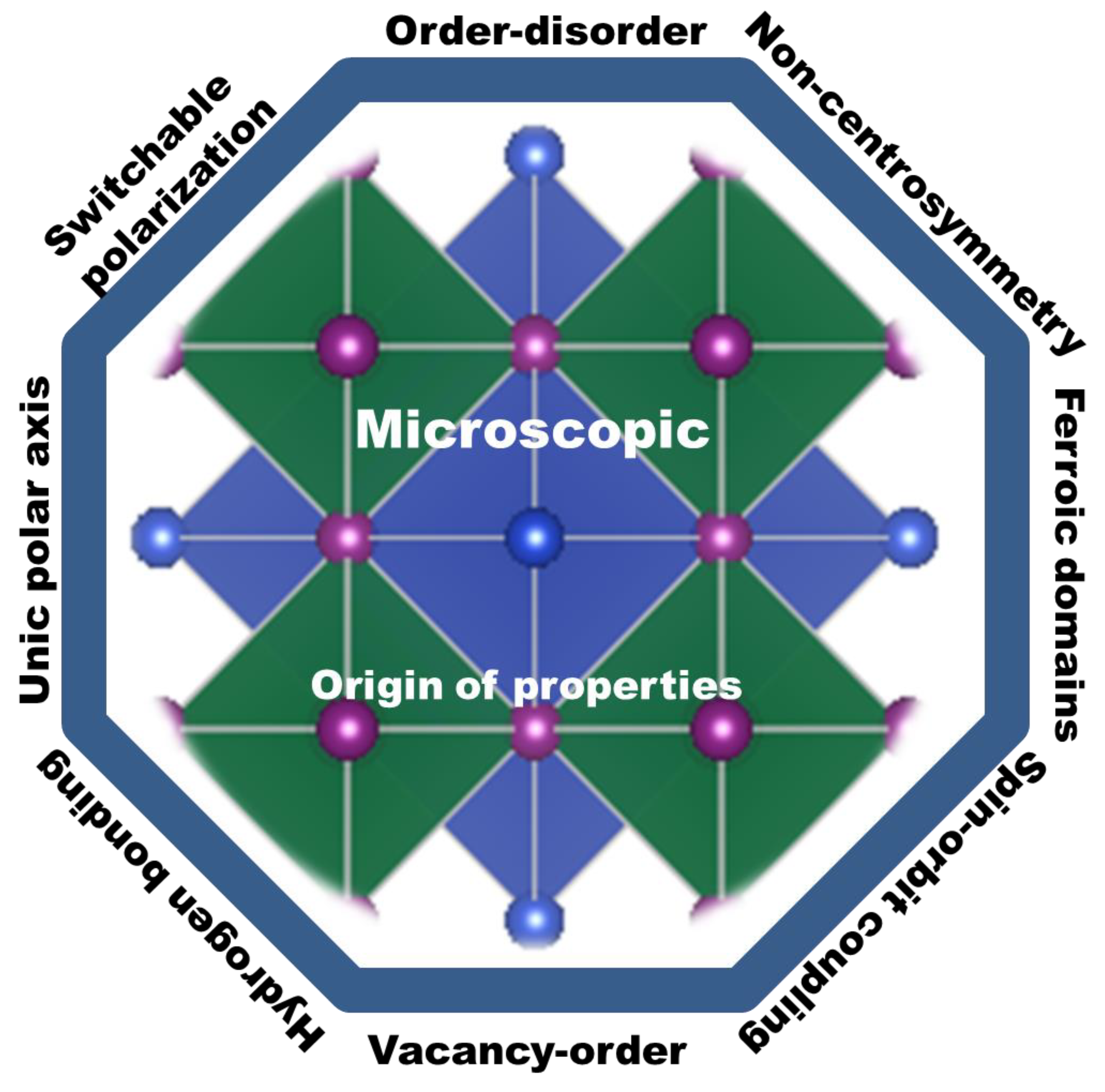
The successful properties of halide perovskites are originated from both macroscopic and microscopic point of view. The macroscopic properties arise from the arrangement and interaction of the constituent cages while the microscopic properties are raised from the behavior and interaction of the atoms, molecules and ions. In particular, the macroscopic properties are property of a substance or matter that can be identified with naked eye and measured with no change of the chemical identity. The mechanisms of action to the microscopic origin and property-functionalization of a given material are atomic and molecular properties such as bond energies, atomic mass and molecular bond lengths causing order-disorder, organic-inorganic interactions, spin-orbit coupling, hydrogen bonding, switchable polarization, local non-centrosymmetry, dipole ordering, multiple polarization directions, ferroelectric domain, polarization, structural transition and unique polar axis, etc.[106,114,171,172,173,174,175] This indicates that understanding both macroscopic and microscopic properties of halide perovskites can lead the way towards their multi-functionalization in wide range applications. And thus, researchers shall dig out both properties for the betterment of the field for suitable applications. For instance, ions such as Bi3+ ions and Pb2+ have two lone pair electrons at their 6s orbital. These electrons haven’t any role in chemical bonding, but their order of lone pairs have the ability to determine the microscopic origin of ferroelectricity.[176]
3.1. Order-Disorder Property
Order-disorder phenomena occur in crystals in which two or more energetically and structurally nonequivalent sites are occupied by two or more vacancies, ions, atoms, or other particles. This order-disorder, In some cases, is linked with an “inversion” or first-order phase change which encompasses a change in crystal symmetry.[177] The order-disorder property is responsible for soft mode phonon and dielectric constant. Ideally, if the order parameter indicates the behavior of phase transition then there is order-disorder property. In this case, the local distortion remains unchanged. This means the octahedral structure remains stable. In order to confirm this property, x-ray absorption fine structure (XAFS) studies are required to be done. Recently there are reports regarding this order-disorder property in halide perovskite materials[176,178,179,180,181,182,183]
3.2. Hydrogen Bonding and Emerging van der Waals
The presence of hydrogen in halide perovskites has been reported elsewhere.[184,185] α- and β-modesα- and β-modes types of hydrogen bonding has been detected.[186] α-interaction mode determines the stability of the octahedral network.[187,188] This hydrogen bonding has essential contribution to the optical, structural and electronic properties of halide perovskites.[189] In addition to this, hydrogen bonding facilitates outstanding decoupling of the crystal growth process and nucleation.[190] It is also reported that hydrogen bonding stabilize the CH3NH3PbBr3 structure.[191] In addition to the presence of hydrogen bonding, emerging van der Waals are important lessons in halide perovskite research. Such van der Waals interactions are responsible for the presence of ferroelectric properties in a given materials in terms of switching kinetics, polar stabilization and polarization origin.[192]
3.3. Switchable Polarization Property
In addition to order-disorder and hydrogen bonding, switchable polarization (polar order) is an indicator of the presence of ferroelectric properties. In halide perovskites, the presence of this property has been detected.[193,194,195,196] Such reversible polarization is carrier activated and organic molecular dipoles affected when exposed to light.[197] The mechanism of light induced polarization is light-induced free carriers due to carrier induced lattice distortion leading to the formation of polarons, occurring below Curie temperature.[198,199] The arrangement of anions and cations under the application of electric field creates dipole moment that act as source of polarization. This dipole moment has ordered polar electric dipoles from which ferroelectricity is originated upon polarization. This is measured though measuring surface current of the ferroelectric material. Therefore, this switchable polarization is expected to make halide perovskites suitable for electro-optic devices, actuators, nanoelectronics and memory applications. In order to achieve successful application, priority towards understanding of the nature of this switching polarization is required. For simplicity, elastic strain, domain size and domain wall energy are joint features that govern the nature of switching polarization.[200]
3.4. Unique Polar Axis
The unique polar axis is an axis where spontaneous polarization takes place along with Curie temperature. But, its direction can be reversed with application of external electric filed. Researchers indicated that only ten point groups have unique polar axis, responsible for the presence of ferroelectrics.[201] Thus, halide perovskites are materials that have unique polar axis responsible for their spontaneous electric polarization induced ferroelectric properties.
3.5. Local Non-Centrosymmetry Property
Halide perovskites have non-centrosymmetry property [202,203,204] the presence of this unique property make them applicable in ferroelectrics, circular dichroism, pyroelectrics, nonlinear optics, circularly polarized photoluminescence, etc.[205] The idea of non-centrosymmetry is separating the center of negative and positive ions to cause permanent polarization in a given material. This polarization is reversible under applied external electric field. The microscopic origins for ferroelectric properties during applied external electric field are the nucleation and growth of domains. Such domains are known as ferroelectric domains. Ferroelectric materials have distinct areas about 1 μm thick and domains, where polarization happens homogeneously.[206] Because of these properties halide perovskites are ferroelectric in nature.
3.6. Ferroic Domains
Ferroelectric domain occurs when there is unit cell retaining polarization having identical orientations. Electric field drives domain wall motion, which activates change in orientation and size of the domain. Furthermore, it can compare the topography of a sample to other local material properties, like piezoelectricity, conductivity or electrical potential in order to investigate microscopic origin of these effects.[207,208,209,210] Especially, piezoresponse force microscopy (PFM) is an AFM tool because of the converse piezoelectric effect and can locally probe the electromechanical properties of piezoelectric samples. Since ferroelectricity is often paired to piezoelectricity, PFM can also imagine ferroic domains.[209,210] Numerous researchers have achieved PFM studies on MAPbI3 films. However, the results of these reports were paradoxical. Furthermore, switchable ferroelectric domains has been demonstrated,[211] which was also supported by consequent PFM studies.[132,212,213,214] Nevertheless, It has also been suggested that they did not come across any proof of ferroelectricity by PFM.[215] In recent times, two reports argued that the MAPbI3 does not shows ferroelectricity at RT according to macroscopic polarization methods and advanced techniques such as PFM measurements.[216,217]
Latest findings[49] revealed that coupling of nanoscale techniques and microscopic offers solid proof for the presence of ferroelastic domains in both CH3NH3PbI3 single crystals and polycrystalline films in the pristine state and under applied stress. Furthermore, experiments explain design of CH3NH3PbI3 ferroelastic domains in polycrystalline films and single crystals can be managed with applied stress, recommending that strain engineering might be utilized to tune the properties of this material.[49] Since the ferroelastic domain boundaries may differ from regular grain boundaries. no proof of concomitant ferroelectricity was experiential and the discovery of ferroelasticity gives an original parameter to regard as in the mission for enabling their widespread adoption and enhancing their stability indicating grain boundaries have an impact on the long-term stability of halide perovskite solar cell device.[49] PTIR technique has been used in order to continuously characterize the domains at the nanoscale and examine in situ whether they are vulnerable to electrical bias[218,219] has attracted much attention for caballing label-free composition mapping,[220,221,222,223] material identification,[224] and conformational analysis[225,226] at the nanoscale.
3.7. Rashba and Dresselhaus Effects
The interaction among the orbital in motion and the electron’s spin round the nucleus is spin-orbit coupling, where this phenomenon is core to spinotronics and magnetism by driving magnetic damping, spin relaxation and magnetic anisotropy.[227] This application motivates researchers to work out their effort on halide perovskite field. For this purpose, MAPbI3 based spin-optoelectronic devices have been reported elsewhere.[228] Highly spin polarized magnetization has been reported for MAPbI3.[229,230,231] Exotic spin-splitting phenomena, for instance, Dresselhaus and Rashba effects[232,233,234,235,236] usually are observed in the relativistic electronic structure of nonmagnetic semiconductors.[237,238,239] The phenomena might give rise due to spin-orbit coupling (SOC), the presence of relatively heavy elements together with the non-centrosymmetry of ferroelectric materials. A “dynamical Rashba effect”, which indicates that even in universal centrosymmetric structures, is revealed by molecular dynamics simulations. The combined inorganic-organic degrees of freedom can generate a spatially modulated Rashba effect, which is differentiated using the MA dynamics at the sub-picosecond time scale.[125,240,241,242] This recommends that the local non-centrosymmetry owing to the local ordering of dipoles at unit cell scale is still vital question to think though a universal centrosymmetry might occur at macroscopic scales. Nevertheless, the theoretical simulation of halide perovskites is enormously difficult as it engages the treatment of numerous subtle, but vital aspects that are complex to figure precisely.
Moreover, considering the relaxed unit cell structures suggested elsewhere[113] and the supposition of total organic cation ordering, Hu et.al.[172] calculated the spin-orbit splitting in energy band structures and the principally likely electric polarization. This is of enormous significance because the Rashba splitting have been proposed to decrease the electron-hole recombination rate and to enlarge the carrier’s lifetime.[243,244,245,246,247] Hence, Hu and his coworkers[172] have calculated the spin-orbit energy-band splitting for all the 12 ABX3 relaxed structures,. Even though obvious tendency among the magnitude of the atomic spin-orbit splitting, ferroelectric polarization, and analogous Rashba parameters are challenging to deduce, in consequence of the difficult relationship between the organic cation/framework atomic relaxations and electronic structure. Because the spin conduction bands and properties of valence are vital for dropping the anticipated spin-splitting parameters for the entire sequence of halides and the recombination rate can assist to comprehend the fundamental characteristics of the exceptional functionalities of halide perovskites solar cells. The Rashba effect is explained using the supposed Bychkov-Rashba Hamiltonian as in equation 1 and is the outcome of the breaking of inversion symmetry in the crystal in a direction orthogonal to a k-point sampling plane.[248,249,250]
withis the polar direction, σ0 and σ=(σx,σy,σz) are the identity and spin Pauli matrices and αR known as the Rashba parameter, respectively. To attain the highest Rashba parameters for a known compound, the low energy Hamiltonian has been extracted with a set of maximally localized Wannier functions.[251] The Rashba splittings and its equivalent band structure of MAPbI3 are greatly anisotropic.[172] It is hence vital to think about this anisotropy[252] when reporting the Rashba parameters. Bulk MAPbI3 crystal has large static Rashba effect.[253] For instance, for the MAPbI3, the momentum offset k0 in valence band can differ from 0.06 to 0.08 A-1 while the its αR can differ from 1.35 to 1.85 eVA.[172] The importance of this effect is slowing down the recombination effect in MAPbI3.[253,254] Dynamic ferroelectric polarization also protects charge carriers from being scattered by defects in MAPbI3 perovskites.[254] Another debatable report clarifies that both MAPbI3 and Cs0.05(FA0.83MA0.17)0.95Pb(I0.83Br0.17)3 are non-ferroelectric semiconducting materials.[255] Unlike Cs0.05(FA0.83MA0.17)0.95Pb(I0.83Br0.17)3, this report is against many literature reports. Although it is different report from the existing research reports, it induces more research work to be done. This ferroelectric property of halide perovskites need more deep research work to reach a conclusion that MAPbX3 perovskites are ferroelectric[256] or not.
3.8. Vacancy Ordered-Provskites
Owing to their ion migration, ferroelectric, pyroelectric, piezoelectric and optoelectric properties, halide perovskites become hot research field. Not only this but also flexibility to integrate into a system and high energy density as well as vacancy ordered material properties enable halide double perovskites applicable to energy storage devices and energy harvesting as demonstrated by double halide perovskites such as MA2SnX6 for Li ion battery,[104] Cs2NaBiCl6 for battery and TMCM2SnCl6 for nanogenerator[257] and Cs2SnI6 for transistor.[258] Moreover, development of high-power rechargeable battery requires high mobility of Li+ overcoming diffusion barrier. Thus, the Sn based double halide perovskites have periodic Sn vacancy narrowing the diffusion barrier in materials such as MA2SnX6 for Li ion battery.[104] Hence, such periodic metal vacancies are highly useful for high efficiency Li based metal batteries and thus, researchers shall dig out more to revolutionize the area of storage devices.
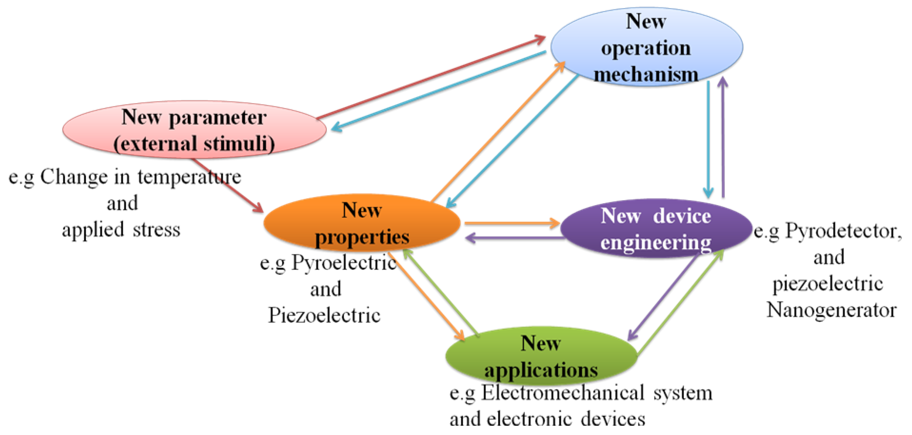
4. Multifunctional Properties beyond Ferroelectrics
Halide perovskites based solar cell has been revolutionizing the field of photovoltaic with power conversion efficiency of 29.13%,[1] breaking the maximum limit for silicon solar cell. This is because of their interesting properties such as tunable absorption of light, superior charge-transfer properties, tunable band gaps, diffusion length and facile processing.[259,260,261,262,263] Beyond photovoltaic, there are other fascinating applications due to their new promising properties such as ferroelectrics, piezoelectrics, pyroelectrics and coexistence of multiple properties.[264] Interestingly, the coexistence of two or more properties makes materials suitable for wide range applications such as in photovoltaic, optoelectronic, thermoelectric, magnetism, ferroelectric and magneto-ferroelectric applications at the same time. For this purpose, the multifunctional properties of halide perovskites of both types: organic inorganic hybrid halide perovskites and all inorganic halide perovskites shall be discovered for wide range applications. Moreover, the coexistence of multiple properties is yet discovered and thus needs more attention. Because of this attention, some research work has been reported elsewhere.[265,266,267,268,269,270] As shown in Scheme 5 Halide perovskites are multifunctional materials required for various applications.
Scheme 5.
New operating stimuli and operation mechanisms with new electrical property for new electromechanical and electronic applications proposed for the field of halide perovskite.
Scheme 5.
New operating stimuli and operation mechanisms with new electrical property for new electromechanical and electronic applications proposed for the field of halide perovskite.
Before directly discussing the details of ferroelectrics, pyroelectrics, piezoelectrics and dielectrics properties of halide perovskite materials, it is of great interest and importance to present the overview of these electronics properties at first. Accordingly, in order to maintain the analogy, the term "paraelectric" should properly refer to polar dielectrics, which consist of grains with polar region oriented randomly in the solid so as to result in no net dipole moment (i.e., no net polarization). This phenomenon is the electrical equivalent of paramagnetism and generally describes the condition of virgin (unpoled) ferroelectrics below the Curie temperature, TC. Because the grains/domains are polar, they are also piezoelectric. All but one of the 21 non-centrosymmetric crystallographic point groups are piezoelectric (the symmetry elements combine in the cubic group 432 to yield no net piezoelectric effect). Furthermore, Ten of the 21 non-centrosymmetric groups include a distinctive polar axis and are, consequently, suddenly polarized. These are the "pyroelectric" materials, in which a variation in temperature results in a variation in polarization. The reverse process is called the "electrocaloric" effect.[271] Several pyroelectric materials have extra property that the direction of impulsive polarization can be varied by a mechanical stress or applied electric field. When it is primarily due to stress, it is "ferroelastic"; when the variation is mainly owing to an electric field, the material is "ferroelectric".
A piezoelectric or pyroelectric is not necessarily ferroelectric, but all ferroelectric materials are also pyroelectric and piezoelectric as shown in Figure 2(1). Ferroelectric materials above their TC are generally called "paraelectric", even if the similarity between ferroelectricity and ferromagnetism falls apart here. Although a ferroelectric would lose its dipoles altogether above TC and become just a non-polar dielectric, a ferromagnet would become paramagnetic above TC. This material is centrosymmetric and so includes no dipoles at all; but, polarization can be induced by an external field in such a way as to expel or reduce the electrostatic energy from the solid. This incidence is fundamentally the electrical equivalent of diamagnetism except that diamagnetisms would also have negative susceptibilities. Moreover, coexisting properties shall also be studied in the field of the halide perovskites.[272,273]
Figure 2.
Illustration showing functional relationships: Reproduced with permission.[274] Copy right 2013 Macmillan Publishers Limited. 1) All ferroelectrics are pyroelectrics, piezoelectrics, dielectrics, but not necessarily the reverse one; all piezoelectrics are dielectrics, but not all dielectrics are necessarily piezoelectrics. 2) Important electrical properties of materials. A) Dielectric materials show charge separation under electric field. B) Piezoelectric materials show an electric polarization when stress is applied from the combination between electrical and mechanical energy. C) A change in temperature induces a net polarization in pyroelectric materials. D) The application of an electric field reverses the polarization in ferroelectric materials. All these materials are both piezoelectric and pyroelectric.
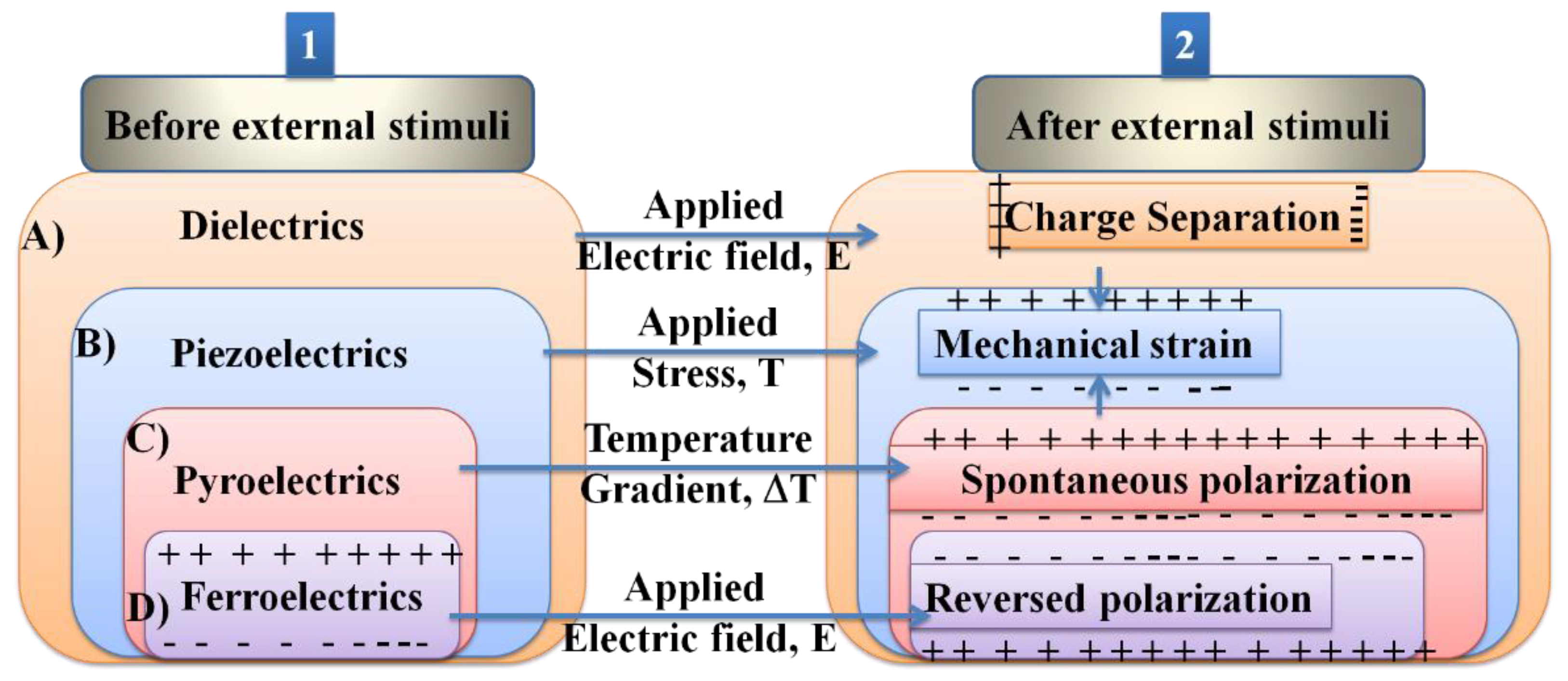
Moreover, the intrinsic electric polarization character of the ferroelectric materials can be altered by an applied electric field. Nowadays the ferroelectrics become highly attractive for several technological devices that utilize their pyro-, piezo-and ferroelectric properties (Figure 2(2)), with the great functionalities possibly for ferroelectric non-volatile memories.[275] These materials normally undertake a phase transition into a low-temperature ferroelectric (polarized) state at the Curie temperature TC from a high-temperature non-polarized paraelectric state,[276] which results in the spontaneous polarization. This is due to the structural transition as well as usually small symmetry-breaking distortion which occur at TC,. The low-temperature ferroelectric material always show non-centrosymmetric structure, consequently it does not exhibit inversion symmetry, since this averts the charge separation intrinsic to the electric polarization.[277] An additional event with which an electric field provides variation in dimensions is electrostriction, which is a quadratic effect between mechanical strain and electric field, and can be observed in all dielectric materials, while piezoelectricity abides by a linear relationship.
Ultimately, ferroelectric materials provide highly valuable properties such as ferroelectric hysteresis and high permittivities, high piezoelectric and pyroelectric coefficients, strong electro-optic effects and anomalous temperature coefficients of resistivity. Of all these properties, the formation of hysteresis loop is highly imperative property of ferroelectric materials due to its polarization reversal property.[278] Furthermore, this behavior originates with the use of electric field and a cycling process becomes observed through the positive and negative directions in ferroelectric materials, as represented by Figure 3.
Ec depends on defect concentrations, temperature, voltage waveform, the surface, electrodes, mechanical pressure and stoichiometry. The polarization originally amplifies from zero to a saturation polarization, Ps and leading to decline the electric field, decreases to a remnant polarization, Pr as revealed in Figure 4. Furthermore, the electric field needed to decrease the polarization back to a zero value termed as coercive field, EC.
4.1. Tunable Material Composition
The wide range electronic, structural, magnetic and optical properties of halide perovskites are originated from tunable chemical composition and dimension (1D, 2D and 3D).[204] This tunable property makes halide peroveskite own multifunctional property reasonable for various applications such as ferroelectricity, photovoltaic, thermoelectric, optoelectronics, ferromagnetism, photocatalysis, storage devices, self-powered unit and wireless electronics, etc. Such tunable properties are comparable electron and hole effective mass, point defects and grain boundaries, and high optical absorption and electrically clean defect properties.[280] Moreover, the great attention towards energy harvesting piezoelectric materials is owing to their flexibility to incorporate into a system and promising energy density compared with electrostatic and electromagnetic devices.[281] Thus, piezoelectric properties of halide peroveskite enable them to get greater attention for various energy harvesting applications. The reason for this high energy density of piezoelectric materials is owing to their high crystalline structures, giving dipole moments and nonoverlaping centers of negative and positive charges.[281]
With respect to this general overview, the halide perovskite family is under study this time. This is due to their tunable crystal structure ABX3 and the corner sharing BX6 octahedron with B site cation in the middle in addition to their tunable chemical composition, where ‘A’ and ‘B’ are two cations of different size with +1 and +2 valence, respectively, and ‘X’ is an halide anion, which makes bonds with both A and B. The stability of the halide perovskite structure is described by Goldschmidth tolerance factor t defined as in equation 2,
where, rA, rB and rX are the ionic radii of the A, B, and halogen ions respectively.
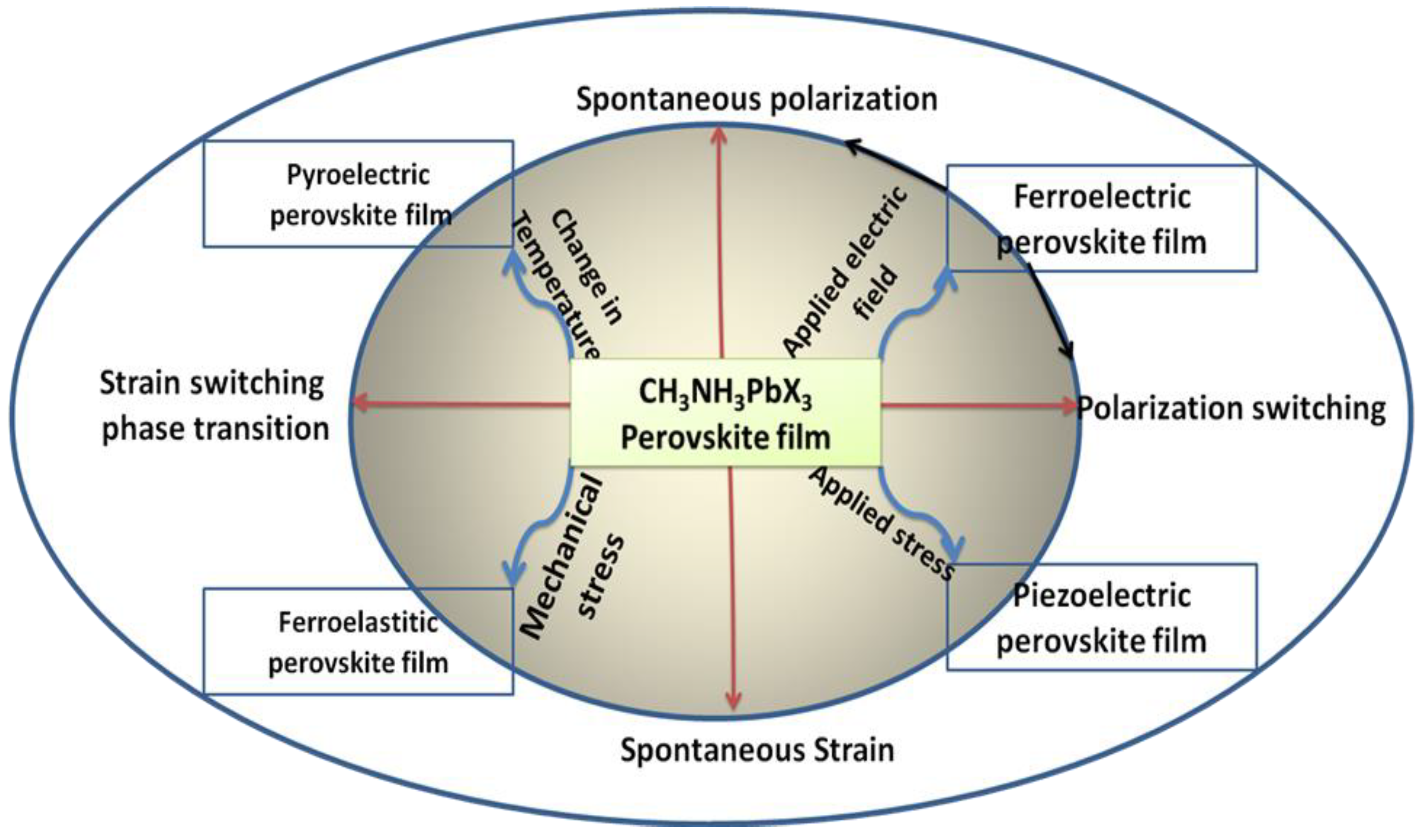
Therefore, it is highly relevant to confirm and identify whether ferroelectric, piezoelectric, pyroelectric and ferroelastic properties are really demonstrated by halide perovskite materials. In addition to these essential properties, there are very important processes such as spontaneous polarization, polarization switching, spontaneous strain and strain switching that help us confirm the presence or absence of these properties under the essential operating conditions of temperature, electric field and mechanical stress (tensile and compressive stress) as summarized by Scheme 6 and understanding the mechanisms and the photovoltaic switching mechanisms and their origin in halide peroveskites is not yet well touched. It is also important to consider other operating conditions that induce concern of degradation and stability issues suggested by Bing Joe et.al.[160] such as moisture, light, excessive temperature and others affecting the success of this study.
Scheme 6.
Representation of stress and field induced electrical properties of OMH Perovskite materials.
Scheme 6.
Representation of stress and field induced electrical properties of OMH Perovskite materials.
Understanding and identifying the unit and important parameters related to paraelectric, piezoelectric, pyroelectric and ferroelectric properties of currently reported organic inorganic hybrid perovskites is essential lesson in this field.[106] Because of this, such unit and important parameters regarding ferroelectrics and piezoelectric properties of organic inorganic hybrid perovskites are reviewed well elsewhere. Such parameters are crucial to understand ferroelectric functional and structural diversity of these materials. This indicates that there are various organic inorganic hybrid perovskites for various applications in the practical thermoelectric applications.
4.2. Ferroelastic New Properties
Another important electrical property of perovskite materials is a ferroelastic phase transition, which shows the ways to a distortion of the crystal lattice resulting in a spontaneous strain in the material – analog to the magnetization / spontaneous polarization in ferromagnetic/ferroelectric materials.[174] Upon the appliance of an external stress, this spontaneous strain can switch its direction in the crystal lattice.[282] Thereby, the formation of twin domains oriented along different crystalline axes lowers the internal strain. For instance, a tetragonal structure let spontaneous strain orientations along the a1, a2 and c axes.[283] Like ferroelectricity, ferroelasticity and magn etoelasticity[284,285] is usually viewed in perovskites with ABX3 structure and is a nonlinear property.[282,283] Recently, ferroelectricity has been suggested to be possible mechanism to clarify the high solar cell PCE in halide perovskites; although realistic experimental proof supporting this premise becomes absent. Distinguishing and identifying ferroelectricity as of another characteristic, for instance piezoelectricity, ferroelasticity, etc., is normally appreciable since this occurrence can coexist in many materials.
Ferroelastic twin boundaries as typical grain boundaries have been identified in CH3NH3PbI3.[286] Such ferroelastic twin boundaries influence neither on the charge carrier dynamics nor behave as non-radiative recombination centers but easy to fade.[286] Figure 4a-c shows x-ray diffraction peak (a) and images of the MAPbI3 single crystal using polarized optical microscope (c) while Figure4d-f shows optical images of domain pattern in MAPbI3 single crystal using polarized light before the application of external stress (d), under tensile stress (e), and after reliving the stress (f).
Figure 4.
Polarized optical microscope confirming presence of ferroelastic domain pattern in MAPbI3 domains. Reproduced with permission[286] Copy right 2020 Nature publishing group.
Figure 4.
Polarized optical microscope confirming presence of ferroelastic domain pattern in MAPbI3 domains. Reproduced with permission[286] Copy right 2020 Nature publishing group.
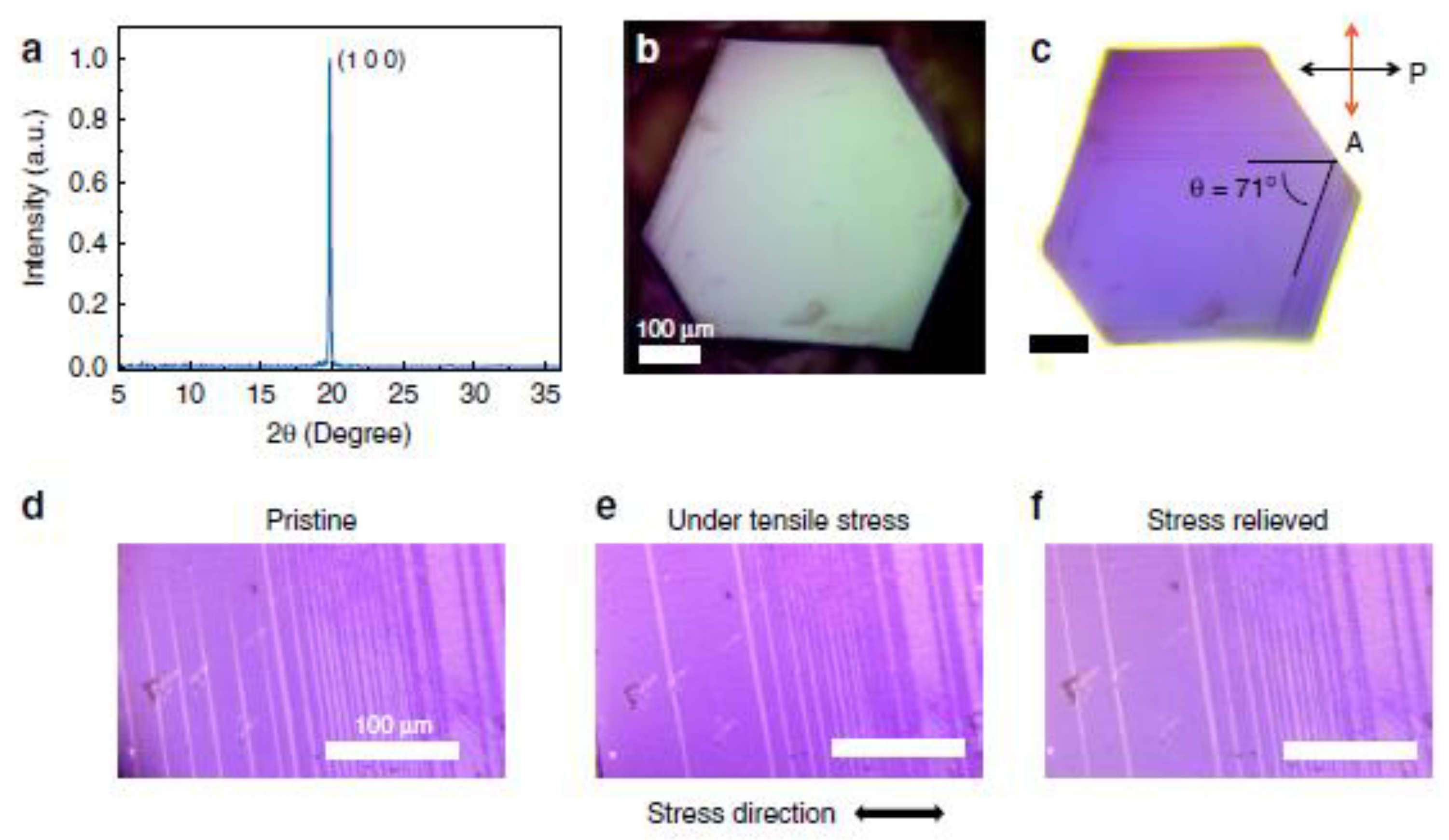
The changed stripe pattern beneath the external tensile stress is confirming the ferroelastic nature of MAPbI3 domains. Moreover, the presence of hysteresis behavior for the motion of such ferroelastic domains are confirmed by the domain boundaries that did not completely return back to the original location after the release of applied strain.
4.2.1. Stiffness and Elastic Compliance
The association resulting strain xij (-) with the stress Xij (N m−2) used ahead of elastic material is shown in Equation 3 given by Hooke’s law:
xij = sijklXkl
The elastic compliance sijkl (m2N−1) is 4th-rank tensor and xij and Xij are 2nd-rank tensors. The converse connection Xij = cijklxkl explains elastic stiffness tensor cijkl (N m−2). The correlation between sijkl and cijkl is sijklcklmn = cijklsklmm = δimδjn. The stress and strain are symmetrical second-rank tensors, i.e. Xij = Xji and xij = xji. The symmetry of the stress and strain tensors need that sijkl = sjilk , hence most autonomous elements of the stiffness tensors and compliance is decreased from 81 to 36. By means of thermodynamics, many of self-governing fundamentals is, consequently, decreased to 21 because sijkl is a symmetrical tensor sijkl = sklij .[287,288,289] Strain tuning is required in halide perovskite ferroelectrics.[290,291]
4.3. Piezoelectric New Properties
Like ferroelectrics, it would of great interest to deal with and understand piezoelectric properties and applications of halide perovskite materials. In order to begin with, the word piezoelectric is used to explain an attractive property of technological important class of materials with a diversity of functionalities, ranging from ultrasound transducers, fuel injectors and waveguide devices to gyroscopes and accelerometers.[292,293,294] It is of high technological interest to explore the piezoelectric properties of the hybrid perovskites for applications such as piezoelectric generators or energy harvesting devices.[295,296] In this section, origin of piezoelectric, the sunrise of piezoelectric, methods to enhance hybrid perovskite piezoelectric, possibility of constructing dampers and low loss piezoelectric, issues that should not be missed during studying piezoelectric and others important points are discussed well.
In the recent times, CsPb2Br5/PVDF composite based piezoelectric nanogenerator has been reported with working process.[297] Adding CsPb2Br5 into PVDF enhance the current and output voltage, indicating that a self-poled composite that don’t need additional poling is generated.[297] Thus, halide perovskites have great advantage in increasing the poling effect when added. Moreover, metal halide peroveskite has been reported as piezoelectric material applicable for nanogenerators as shown in Fig 2.[298] The result showed a molecular piezoelectric coefficient (d33) of 165 pm/V and maximam peak power density of 43 μW/cm2 at 50 kPa. This is the largest power reported for energy harvesting for EDABCO-CuCl4 based piezoelectric materials. The advantage was obtained from increasing polarization through lattice distortion of CuCl42_. This polarization effect increased the dielectric constant, giving a trade of d33 and g33.[298] Figure5a shows Cu2+−3d orbitals as a projected density of state for EDABCO-CuCl4 where a single state dxy and two double degenerate states dxz and dyz are obtained from splitting triple-degenerate t2 d-levels. Similarly, a single state dz2 and dx2−y2 are obtained from splitting double degenerate e d-levels. This indicates that there is Jahn-Teller lattice distortion. Adding a quasi-spherical cation into this lattice distortion causes enhanced mechanical response giving large d33.
Figure 5b also shows two intense bands as referred by the optical absorption spectrum. While ligand-to-metal charge transfer is observed at the visible band 2.6 eV, the d–d electronic transitions is observed at the near infrared peak with in the crystal field of [CuCl4]2−. This is caused by the Jahn-Teller lattice distortion. The splitting of The Cu2+−3d orbital energy level is shown in Figure5c while the stable structure of EDABCO-CuCl4 is indicated by Figure 5d. Furthermore, 165 pm/V value of high d33 of was obtained as a function of temperature, indicating enhanced mechanical flexibility for EDABCO-CuCl4 (Figure2e). Fig 5f shows the transduction coefficient (g33*d33), where the electrical energy of energy harvester depends on the trade-off piezoelectric voltage coefficient (g33) and piezoelectric charge coefficient (d33).[299,300] Remember that the trade-off between piezoelectric voltage coefficient and piezoelectric charge coefficient for molecular metal halides is not fixed yet. This requires further in depth study.
4.3.1. Origin of Piezoelectricity
Piezoelectric effect is strain development under the application of electric filed. Because piezoelectricity is a basic procedure including multiple piezoelectric equations exist and diverse electromechanical effects.[140,287,301,302,303,304,305] The direct piezoelectric effect relates the produced polarization that build up in i direction (ΔPi) with an applied stress in direction j(σj in Voigt notation) as in equation 4:[306]
ΔPi = dijσj
Where, (dij) is 3rd-rank tensor and every dij is typically called piezoelectric coefficient or direct piezoelectric strain coefficient, in units of pC/N. An additional piezoelectric equation between the polarization with the strain η is specified by equation 5:[306]
ΔPi = eijηj
Where, the eij is the piezoelectric stress coefficient in the unit of C/m2. It is indicated that the dij and eij parameters are associated with each other using stiffness and/or elastic compliances, though dij is simple to determine experimentally. The total generated polarization articulated in the c direction is given by equation 6:[306]
Where,
are strains along the x, y, and z axis, with x0, y0, and z0 are lattice constants for structure not strained.
In order to disclose the source of piezoelectricity,[307] it is important to split the total polarization originated from contributions of the 1) A-site MA cations and 2) B-site Pb atoms. The Pb atom induced polarization is measured using (Pb) × D(Pb)/Vu * PPb = Z33,[306] where Z33*(Pb) is Born effective charge of Pb, D(Pb) is average displacement of Pb alongside the c axis with respect to the center of its I6 cage and Vu is the volume of the primitive unit cell. Thus, +4.24 is measured value from the contribution of Z33* (Pb), considerably greater than the supposed charge of Pb (+2.0) in a pure ionic image[306] that implies the presence of dynamic charge transfer coupled with the change of Pb-I bond length and the strong covalence of the Pb–I bonds. It is obvious that although both molecular dipoles and Pb displacements are in charge of the total polarization, in which Pb atoms contribute nearly all the piezoelectric response, with the negligible contribution from the MA+ molecules.
In perovskites with unusual atomic substitutions in the ABX3 architecture, the competition between B–X metal-halide bond and A–X hydrogen bond monitors the piezoelectric characteristics drawing attention to the prospective of halide perovskite design for manipulative latest useful photopiezoelectrics and photoferroelectrics,[306] such as applications in sensors, actuators, and energy harvesting.[294,297,308,309] Because of the pairing of semiconducting properties with its piezoelectrics, micro- and nanowires of piezoelectric semiconductors have been utilized as fundamental building blocks for developing ground-breaking devices:[310] for instance, piezo-phototronic devices,[311,312] piezoelectric diodes,[313] piezoelectric field-effect transistors,[314] piezoelectric chemical sensors[315] and nanogenerators.[316,317,318]
Thus, halide perovskites possesses a cubic cystal structure that gives rise to ferroelectric polarizations similar to other class of perovskites with identical structural character.[19,319,320,321,322] Coll et al. have demonstrated the polarization switching and light-enhanced piezoelectricity of CH3NH3PbI3 materials.[11] Furthermore, an output piezoelectric of 2.7 V and 140 nAcm−2 have been reported,[323] hindering the practical functionalities due to its modest output performance. Moreover, a highest piezoelectric current density and output voltage of 3.8 μAcm−2 and 8.5 V have been demonstrated from the piezoelectric nanogenerator under periodically vertical compression. Multilayered halide perovskites even have larger large polarization or strong piezoelectricity ≈1540 pCN−1.[324] This output is quite promising compared to other literature reports.[325] This could help charge LED and capacitor through a bridge rectifier.
4.3.2. Enhancing Halide Perovskite Piezoelectricity
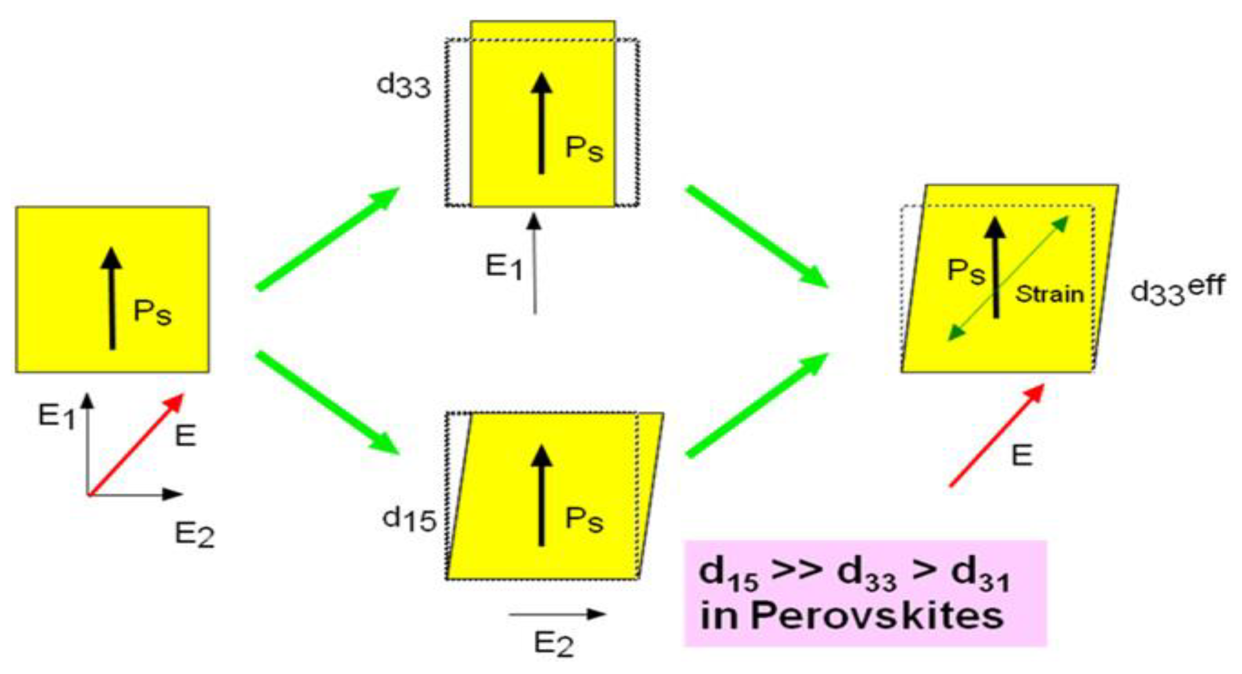
The scientific possibility and the procedure how to enhance piezoelectricity are great concerns in the field of hybrid organic-inorganic or fully inorganic perovskites. It is remarkable that the maximum values are experiential from a rhombohedral composition only when the single crystal is poled along the [001] spontaneous polarization axis for oxide perovskites, but not along [111]. However, this is very important issue for the field of halide perovskites. Furthermore, Figure6 demonstrates schematic representation of an approach on how to enhance and understand these piezoelectricity enhancement procedures in accordance with the crystal orientation in perovskite ferroelectrics. The impression of the present ‘domain engineering’ is approximately similar to the octahedron rotation.
Figure 6.
Schematic of the domain engineering for piezoelectricity enhancement strategy. Reproduced with permission.[326,327] Copyright 1997, IOP publishing. The large d15 is the key for oxide perovskites. What about for halide perovskites?
A d33 value of 2.7 pm/V for MAPbI3 single crystals has been found,[328] close to the value for quartz (~2.0 pm/V)[329], considerably lesser than the values for Pb(Zr,Ti)O3 (~400 pm/V)[330] and ZnO (~12 pm/V)[331]. Additionally, PFM has been used in polycrystalline thin films to confirm the local d33 value of 6 pm/V.[332] To date, no effective material strategy has been developed to engineer polar axis of piezoelectric response. For MAPbI3 film on Au and ITO, the d33 value is ~ 0.3 pm/V, almost two orders of magnitude lower than that of PZT.[333] Recently, the piezoelectric coefficient was found to be ~ 4 pm/V for both polarization directions, with no appreciable dependence on the film thickness.[333] The films on Au and ITO, on the other hand, reveal consistently a low d33 value of about 0.3 pm/V. This value is about one order of magnitude lower than that obtained on bulk single crystal samples[328] Notably, in 1969, physically powerful piezoelectricity was demonstrated in Poly-vinylidene fluoride (PVDF) materials. Since then, PVDFs are used for a variety of functionalities on behalf of PZTs because of its cost, accessibility and other piezoelectric parameters. When poled, PVDF is a ferroelectric polymer, showing competent piezoelectric and pyroelectric characteristics. These properties creates it helpful in sensor and battery functions.[334] Therefore, the use of this material and its derivative may be important research directions for the piezoelectric enhancement of halide perovskite materials. There are also numerous other synthetically fabricated piezoelectric materials like Active Fiber Composites (AFC) and Quick packs™ which are flattering more and more accessible for different functions. However, Lee et al.[335,336] did his experiments to contrast PVDFs and PZTs for energy harvesting functionalities and found that PVDF with a certain electrode configuration proved to have the longest fatigue life and hence more suitable for energy harvesting.
4.3.3. Constructing Low Loss Halide Perovskite Piezoelectric
From the current time onwards and from the energy efficiency improvement perspective, it is time to think about how to realize sufficient output piezoelectric with completely no loss or at least low loss of power as burning issue. In addition to this, raising the mechanical quality factor to amplify the resonance displacement and dropping hysteresis is the prime target from the transducer application perspective. Though halide perovskite materials were reported as piezoelectric materials, there is no literature reporting how to construct low loss piezoelectric from these materials. Before going to construct low loss piezoelectric halide perovskites device, it is important to understand the universal loss mechanisms and loss study method in piezoelectric, magnetostrictors, and smart materials: mechanical quality factors QA for the resonance and QB for the antiresonance in the admittance/impedance curve and deriving physical losses.[337,338] There are three losses in piezoelectric:[339] elastic tan ϕ, piezoelectric tan θ, and dielectric tan δ, where the θ′ obtained in the k31 mode (equation 9):[340]
A common way for calculating the piezoelectric loss, where, tan ϕ′ obtained from the inverse value of QA in the k31 mode whereas tan δ′ obtained from an a capacitance meter at a frequency or impedance analyzer away from the antiresonance range or resonance.[339] Furthermore, parameters from an admittance/impedance spectrum around the antiresonance (B-type) and resonance (A type) range obtained experimentally: ωa, ωb, QA, QB (from the 3 dB bandwidth method[340]), and the normalized frequency Ωb =ωbl/2v. The calculated electromechanical coupling factor k from the ωa and ωb with the IEEE Standard equation in the k31 mode equation 10:
In addition the magneto-electroluminescence property has been reported. Such results are observed as negative, but turn-on voltage in 2D-C6H5(CH2)2NH3)2PbI4-based LED devices is larger than in 3D CH3NH3PbI3 because of larger bandgap and multiple quantum wall in the first.[341]
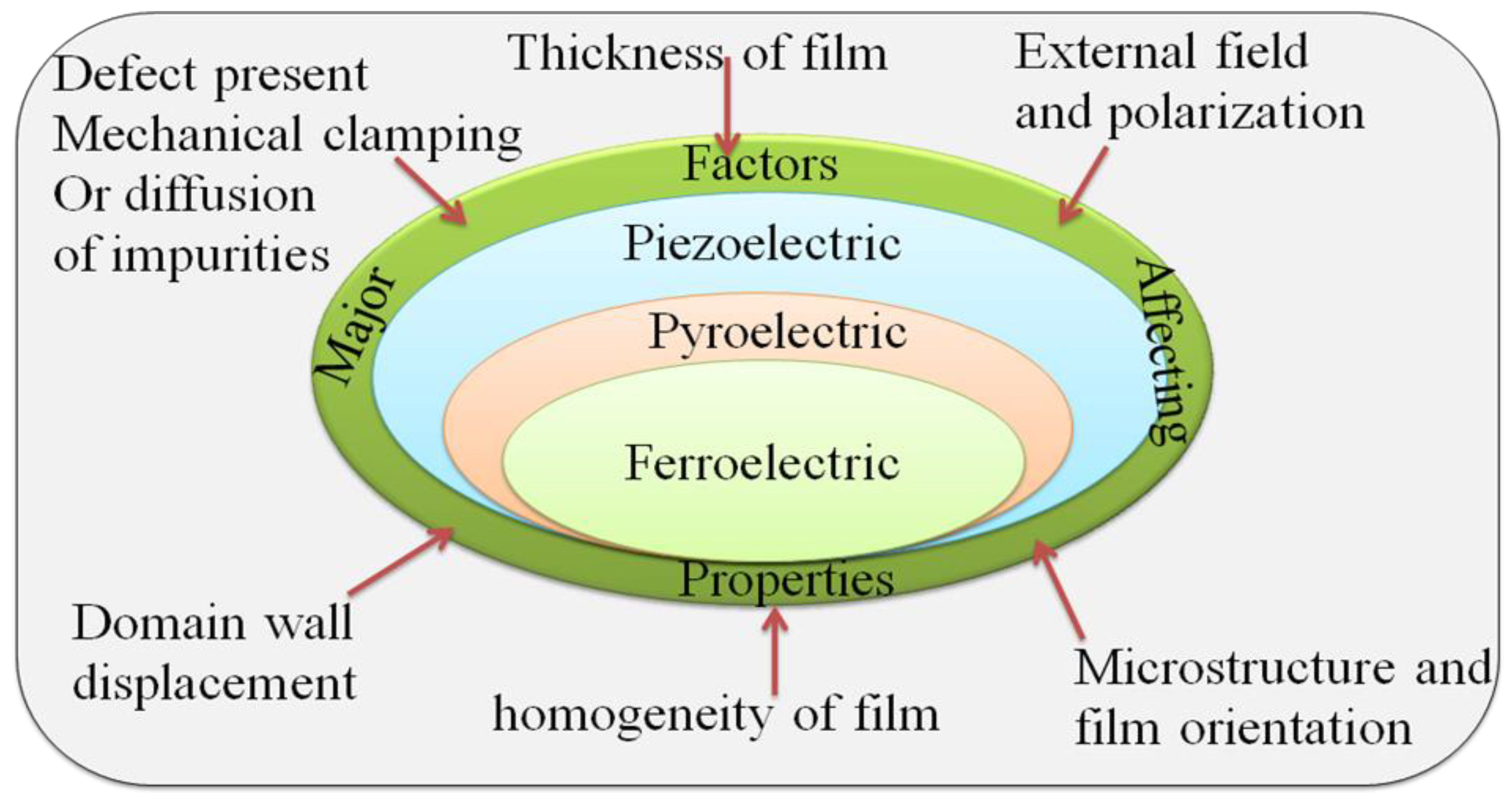
4.3.4. Essential Issues during Studying Piezoelectric Properties
In order to achieve the final goal of piezoelectric materials, it would be important to consider all the issues that could block the realization of these properties and its applications. With respect to this great concern, numerous factors present that apparently affect the piezoelectric response, together with the level of polarization, orientation of the film, mechanical clamping to the substrate and breakdown field strength as shown in Scheme 7. In addition to those factors, the effects of defect on the domain-wall roles to the piezoelectric effect are other effects that have not yet been investigated in more detail. Consequently, it is currently not understandable whether, for instance, the influence of donor and acceptor dopants on the important characteristics of halide perovskite films might give rise to the same effects as in bulk materials or not. Furthermore, studies of the piezoelectric coefficients by means of the converse or direct effect considering the stresses enforced on the film by the substrate because of the diffusing of the film to the substrate. With respect to the converse piezoelectric effect, the efficient piezoelectric coefficient might be simply determined based on piezoelectric constitutive equations[342] for isothermal processes. For example, let us consider a polycrystalline film with arbitrarily allocated grains that is poled along at right angles to the plane of the substrate (the z-axis). For perfect clamping in the plane of the substrate (x–y plane), x1 = x2 = 0 and x3 ≠0. Similarly, X1 = X2, because of the symmetry of the film in the plane of the substrate and X3 = 0 for the reason that the surface of the film is free. Piezoelectric constitutive equations then gives the piezoelectric coefficient[343] for the efficient converse d33 in arbitrarily oriented films (distinguish the appendix elsewhere in reference[342]) given by equation 11:
Because in the majority of materials, s13 < 0, d31 < 0 and d31 is comparatively huge (in PZT d31 is approximately 1/3 of d33), the calculated coefficient in films is at all times lesser than in unclamped materials.
Scheme 7.
Representation of proposed factors affecting piezoelectricity: All factors affecting ferroelectricity affects both piezoelectricity and pyroelectricity.
Scheme 7.
Representation of proposed factors affecting piezoelectricity: All factors affecting ferroelectricity affects both piezoelectricity and pyroelectricity.
4.3.5. Measurement of Piezoelectric Coefficients
In principle, both procedures let to compute the piezoelectric coefficient d33,charge constant described by equation 12 or 13:[344]
or
Where, E the electric field, S is the strain, T the stress, and D the electric displacement. The x3 axis is the direction of polarization (poling). This is the direction at right angles to the surface for thin films. Note that one has to take into account that the thin film is at all times clamped to a substrate during the measurement of the piezoelectric properties of thin films. So, the ratio S3/E3 (or D3/T3) does not stand for the piezoelectric coefficient d33 of the free sample other than an effective coefficient. This effective piezoelectric coefficient dss(ip) is correlated to the actual coefficient d33 (equation 14) for the inverse piezoelectric (ip) effect where a voltage is used to persuade a strain which is computed:[344]
Where, d33 is the transverse piezoelectric coefficient and parameters such as s13, s12, and s11 are the mechanical compliances of the piezoelectric film. Because the values of d31, s12 and s13 are typically negative but the value for s11 is positive and greater than s12.
On the other hand, the piezoelectric coefficient can also be determined from layered heterostructure such as MAPbI3/PTZ layered heterostructures in which the greater part of the bias voltages were constantly applied in the course of the MAPbI3 layer, in which the fraction of voltage (νMAPbI3 = VMAPbI3/Vbias) varying between 87% and 93% because of the enhancements in film thickness from 20 nm to 60 nm.[333] Once the voltage fractions across the two layers (νPZT = VPTZ/Vbias) have been determined, the d33 value of MAPbI3 calculated using equation 15:
In this case “-” for out-of-phase (destructive) and “+” for in-phase (constructive) piezoelectric responses between these two layers has been determined. It has also been extracted a value of = 3.7±0.1 pm/V for the region that is in-phase with the piezo-response of bare PZT and 4.2±0.2 pm/V for the out-of-phase region.[333]
4.3.6. Piezoelectric Effects
Besides an electric field using a mechanical stress, piezoelectric materials are a class of materials which can be polarized, (Figure 7). The direct connection between stress Xik applied to a piezoelectric material and resultant charge density Di is the direct piezoelectric effect and shown in equation 16.
Di = dijk = Xjk
Where, dijk (C N−1) is a 3rd-rank tensor of piezoelectric coefficients. Whereas another interesting property i.e applied electric field induced converse piezoelectric effect that explains the strain in a piezoelectric material given by equation 17):
Where, t is the transposed matrix. The units of the converse piezoelectric coefficient are .mV−1.
Furthermore, easier molecular model used to explain the piezoelectric effect is given by Figure 8 and is the production of an electric charge because of a force exercised on the material. Moreover, the centers of the positive and negative charges of every molecule happen together prior to subjecting the material to an external stress—ensuing into an electrically neutral molecule as illustrated in Figure 8a. On the other hand, in the existence of an external mechanical stress the internal reticular can be distorted, thus raising the division of the positive and negative centers of the molecule and producing little dipoles as shown in Figure 8b. Consequently, the contrary facing poles within the material revoke each other and fixed charges emerge on the surface. This is demonstrated in Figure 8c. This effect in the material which is polarized is said to be direct piezoelectric effect and produces an electric field engaged to change the mechanical energy, engaged in the material’s distortion, into electrical energy. Although halide perovskites have not been reported to exhibit reverse piezoelectric effect, a number of materials demonstrate the reverse piezoelectric effect.
4.4. Pyroelectric New Properties
Like the ferroelectric and piezoelectric properties, it is crucial to consider pyro-electricity in order to understand the electronics properties and related applications of halide perovskites. Furthermore, pyro-electricity is an important property to express the crystallographic character of the material without external fields. Accordingly, the MAPbI3 has a noncentrosymmetric structure is polar and, which will hopefully put a closing stage to the uncertainty about the space-group of the tetragonal halide perovskite, which is I4cm rather than I4/mcm. Moreover, understanding whether this symmetry is impressive and special to MAPbI3 or universal to the other its derivative tetragonal symmetries is grateful. The latest information on the lack of SHG in MAPbI3 [346] confirmed the rationale to the uncertainties though this query regarding the symmetry is verified using the existence of pyroelectricity, as well as showing the obvious proof for SHG as well as giving details of why no SHG was presented in ref.[346]
Recently, motivating research outputs have been forwarding such as shown in Figure 9A in which a clear pyroelectric response, Jpyro, in the direction of <001> is observed.[347] Furthermore, the direct proportionality between conductivity and a semiconductor’s thermoelectricity verifies that thermoelectric currents will happen to be further principal at elevated temperatures due to the increase in semiconductor conductivity with temperature. Although at RT the pyroelectric response is still exists, it is greatly small at low temperature, where it becomes the controlling element of the thermally stimulated electric response (TSER). Despite decreased thermoelectricity, inferior electrical conductivity also should usually increase the effective spontaneous polarization and decrease leakage currents which ought to enlarge the pyroelectric response. Likewise, Figure 9B shows further proof for the pyroelectric character of MAPbI3 derived from the peak-current value reliance on temperature. Moreover, the local maximum near the phase transition temperature (Tc) at 330 K reveals an increase in the pyroelectric response as anticipated in the theory discussed elsewhere[348] at a ferroelectricto-paraelectric phase transition. As a result, the local extreme around Tc is a physically powerful sign that tetragonal MAPbI3 is ferroelectric.[349] Determining the imaginary (εim) and real (εre) relative permittivity with respect to temperature demonstrates a dielectric irregularity around Tc (Figure 9C), as well formerly examined in MAPbI3films[350], which holds up the termination that tetragonal MAPbI3 is ferroelectric.[351,352] The fading and regeneration of the pyroelectric response following beyond the Tc provide additional shore up to the non-polar character of the cubic phase and the polar nature of tetragonal MAPbI3, which agrees with results for MAPbBr3.[353]
4.4.1. Pyroelectric Effect
For studying materials for electronics applications, considering and understanding piezoelectric effect is very important rationale.[354] This piezoelectric effect is defined by the variation of the vector of spontaneous polarization with temperature T as described in equation 18:
Where, pi(Cm−2 K−1) is pyroelectric coefficients vector. Also equation 31 may be rewritten as:
Di = ΔPS,i = piΔT
Where, Di (Cm-2) is the surface charge density and ΔT is temperature change. Furthermore, It should be clearly known that the spontaneous polarization can take place only if an exceptional polar axis (section 10.2[287]) present in a given materials of an interest. With the perspective of pyroelectrics, these materials are the property of subset of noncentrosymmetric point group with 10 polar crystallographic point groups. Accordingly, while all pyroelectric materials show piezoelectric behavior, only a few piezoelectric materials whose symmetry belongs to polar groups behave pyroelectrics such as CH2CF2/n, Pb.Zr;Ti/O3, and ZnO, but organometal halide perovskites are under investigation to own these essential properties.
In the recent time, synergistic photoexcited and photovoltaic pyroelectricity has been reported as an efficient method for guiding the charge carrier behavior of electronic and optoelectronic applications.[355,356,357] This synergy of two effects is caused by the light-matter interaction. During light matter interaction, polarization electric field causes stable photovoltaic current while thermal redistribution results in instantaneous pyroelectric current. Such coupling of unique physical properties and spontaneous polarization make halide perovskites such as (NPA)2(EA)2Pb3Br10 (NPA = neopentylamine, EA = ethylamine) possible candidate for light induced pyroelelctric effect research. Such property of halide perovskites are useful to develop light induced pyroelectric effect based self-powered X-ray devices better than heterojunction based self-powered devices. Thus, halide perovskites are not only useful in photovoltaic and electronic but also in novel self-powered X-ray optoelectronic devices. Such novel self-powered X-ray optoelectronic devices are because of the energy harvesting property of halide perovskites. Moreover, this alignment of coupling photovoltaic and pyroelectric properties gives enhanced open-circuit voltage and transient short-circuit current, boosting device performance.[358]
As shown in Figure10, recently, it was possible to develop device architecture (Figure10a), working mechanisms (Figure10b) and self-powered ZnO/peroveskite hetero-structured performances enhanced via Pyroelectric effect (Figure10c-e). During ultraviolet illumination, polarization induced Pyroelectric effect owing to non-central symmetric crystal structures is created. This Pyroelectric effect is produced owing to the temperature increased during Ultraviolet illumination of the sample. This Pyroelectric effect present at the interface facilitates charge transfer and reduces possibility of recombination. This increases enhance the open-circuit voltage and transient short-circuit current.[358] Figure10c-d showed the presence of Pyroelectric effect and photovoltaic effect together at some stage where there are temperature gradients but the Pyroelectric effect disappeared at the stage where temperature becomes constant. The halide peroveskite power conversion efficiency would be the result of the synergistic effect of both Pyroelectric and photoelectric effects, together boosting the efficiency under light illumination. This is good opportunity for halide peroveskite to have energy harvesting and photo-sensing wide applications including in nano-sensing. In Similar fashion, such photo-Pyroelectric effect has been observed in N-isopropylbenzylaminium trifluoroacetate (N-IBATFA).[359] Furthermore, for better understanding the result, specific detectivity, D*, has been measured as shown in Figure 10e. In all cases, the Pyroelectric effect is responsible for both photoresponsivity and detectivity, where D* = R(2e.Idark/S)0.5.[358] Note that R = (Ilight – Idark)/Pill, where Pill = Iill x S. S is the effective area of the photodetectors, R is the corresponding photoresponsivity, Pill is illumination power and Iill is short circuit current with illumination.
4.4.2. Non-Centrosymmetry and Spontaneous Polarization
From the perspective of crystal symmetry of materials, clear understanding of symmetry element and symmetry group has its own vital role in determining the properties of materials whether it is a thin film, a crystal, an amorphous material or a polycrystalline and is displayed as in scheme 8.
For instance, if a physical characteristic is themed to a symmetry element of the material, this characteristic should not alter its value.[287] Rather, it pursues from the Neumann’s principle that a number of characteristics, for example, pyroelectricity and piezoelectricity can be presented merely in materials with sure symmetries and that other properties for instance elastic compliance, electrostriction and dielectric permittivity) are present in all materials. Furthermore, the symmetry requirements could considerably decrease the number of independent and nonzero elements of a property tensor. Moreover, the piezoelectric and other effects explained via odd-rank tensors are not allowed through the symmetry in crystals that belong to 432 noncentrosymmetric point group and eleven centrosymmetric groups. Accordingly, crystals that belong to the remaining twenty noncentrosymmetric groups from the total thirty two point groups can show the piezoelectric effect and are occasionally called piezoelectric point groups from which ten of the piezoelectric point groups could show and own a unique polar axis without a spontaneous polarization vector, PS, the pyroelectric effect present and an external electric field.
Scheme 8.
halide perovskite crystal symmetry showing ferroelectricity, piezoelectricity and pyroelectricity effects.
Scheme 8.
halide perovskite crystal symmetry showing ferroelectricity, piezoelectricity and pyroelectricity effects.
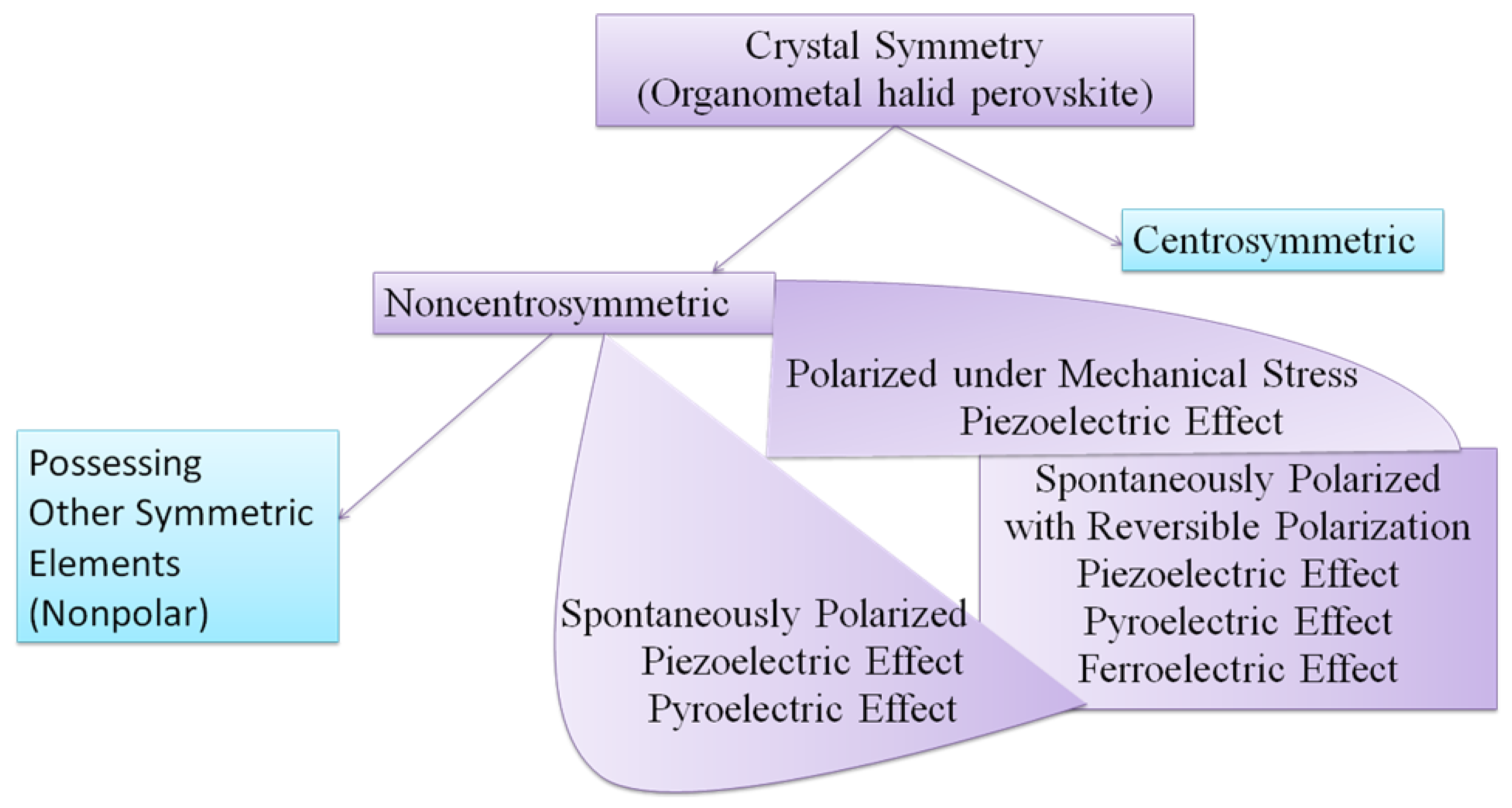
4.4.3. Strain Properties
From the perspective of synthesis procedures, it would be crucial to consider the strain properties happened during materials preparation and due to other factors. Consequently, this concern is highly important in the field of halide perovskites that perovskite films synthesized using various procedures have analogous lattice strain indicating the strain should derived from a shared process that all these halide perovskite films have practiced. The XRD measurements of the MAPbI3 thin films on ITO substrates at 100°C were not strained. Since thermal expansion of the lattice possibly will account for the peak shift, the peak shift of the scraped MAPbI3 powder was measured over the same temperature range. However, its peak shift is much smaller than that of the thin film (Figure 11C and D), indicating that the peak shift observed in the thin-film materials are mainly due to the introduction of strain. Considering the large thermal expansion mismatch between the ITO/glass substrate and the perovskite, strain formation during cooling (Figure 11A and B) has been proposed.[58] When the perovskite forming at 100°C cools to room temperature, it tends to contract due to the positive thermal expansion coefficient (Figure 11A).
As shown in Figure 12, mixed halide perovskites such as (FAPbI3)0.85(MAPbBr3)0.15 have inhomogeneity, resulting strain properties.[360] Not only these mixed perovskites but also MAPbI3 has inhomogeneity.[361] This inhomogeneity is believed to be source of strain in halide perovskites. The tensile strain was observed decreasing up on flipping heat treatment procedure (Figure12a-b). This indicates homogeneity of the lattice structure is small at smaller strain. Furthermore, compressive strain was observed in the as-synthesized peroveskite film, indicating the solvent left pinhole after annealing since it didn’t distribute smoothly during annealing process (Figure 12c, d). This caused trap-assisted recombination as shown in Figure 12d. Thus, the power conversion efficiency is observed with or without tensile strain, strains free and compressive strain as shown in Figure 12e-f. Such strains are cause by the temperature gradients during film preparation.
The presence of strain and gradient distribution in the film shows there is structure inhomogeneity serving as recombination center thereby reducing charge transfer and device efficiency. This suggests that energy harvesting devices can be fabricated via strain engineering like memory and sensors devices, particularly in the electronic devices, for instance, nonvolatile memory,[362,363] tunable capacitors,[364] solar cell,[365] and tunnel junction.[366] Furthermore, there are two approaches to increase piezoelectric energy harvesting to generate power: increasing strain via applied stress and coupling mode. Such coupling mode depends on applied force and material poling directions.
4.5. Thermoelectric Properties
Thermoelectric materials are essential for thermoelectric applications. For this purpose halide perovskite are recently reported as thermoelectric materials. [367,368,369,370,371,372,373,374,375,376] Outstanding thermoelectric performance is expected from N-type semiconductors and thus Cs(Ge,Sn)I3 becomes a possible alternative material.[368] It’s See-beck coefficient increases as its band gap increases. This makes it suitable for thermoelectric applications. Moreover, CsSnBr3 is an additional thermoelectric property recently reported with promising results. [367] Its ZT value was maximized at ~0.01 and its promise indicates that its thermoelectric performance can increase with doping engineering.[367,377,378] It was observed that photoexcitation was an effective way to enhance electrical conductivity and See-beck coefficient through excited states in CH3NH3PbI3.[379] Cs3Cu2I5 has also been reported as candidate thermoelectric material for possible thermoelectric applications.[380] The result indicates that this material is a possible n-type candidate material corresponding to a thermodynamic heat-to-electricity power conversion efficiency of 15% and a thermoelectric figure-of-merit ZT of 2.6.[380] Thermoelectric figure-of-merit ZT is given by ZT =σS2T = PT/k, where P(=σS2) is the thermoelectric power factor, k is the thermal conductivity, T is temperature and σ is the electrical conductivity and S is See-beck coefficient (a measure of the thermoelectric property). Thermoelectric materials with superior See-back coefficient are adaptable and vigorous for waste-heat recovery. Both electrical conductivity and See-beck coefficient are dependent on carrier concentration; charge carrier mobility, temperature, relaxation time, average band effective mass, Fermi–Dirac distribution function and density of state. A material to have multiferroicity, ferroelectricity or piezoelectricity it has to possess non-centrosymmetry, but to be thermoelectric it is not constrained by symmetry.[381] It must be known that thermoelectric conversion merit requires high electrical conductivity (s) and low thermal conductivity (k). This requirement makes thermoelectric materials difficult to engineer.
Even if promising research work has been done in the field of halide perovskites, much work is remaining yet discovered. It is time discover much research result to make halide perovskites applicable for thermoelectric applications. Essential parameters such as Hall coefficient and thermal conductivity, electrical resistivity, and calculation of the charge carrier concentration, See-beck coefficient and mobility shall be discovered for better understanding of the thermoelectric properties and applications of halide perovskites. The application of thermoelectric materials is in cooling such as in optoelectronics, small scale refrigeration and detectors as well as power generation such as in deep space missions.[382] Halide perovskites shall be tested whether they can succeed or not in these potential thermoelectric applications with deep understanding.
From the thermodynamic approach, understanding and considering the coupling mechanisms among the electrical, thermal and elastic parameters and their synergistic effects on the performance of halide perovskites would be vital for the future development. The outcomes are equations of state which present relationships among material parameters computed under different experimental conditions and the coupling mechanism is via the thermodynamic approach. These relationships are necessary for understanding and modeling the response of ferroelectric, ferroelastic, pyroelectric and piezoelectric devices. Moreover, the coupling thermodynamic approach is presented in the next discussion and broadly elsewhere.[289,383,384] From the first and second laws of thermodynamic concepts, the reversible change dU in the internal energy U of an elastic dielectric subjected to a small change of the, entropy dS, strain dx and electric displacement dD is shown in equation 20.
dU = TdS + Xijdxij + EidDi
Where, T is the temperature of the material. Under isothermal circumstances using electric field and stress, it is practical to alter the set of self-governing variables from (S, x, D) to (T, X, E). In order to alter the independent variables from the initial set to the other applying Legendre transformation of U using additional term −Ts −Xx − ED to U becomes crucial. The resultant free energy relation as in equation 21:
is called the Gibbs free energy. The differential of G offers in common with equation 22
G = U − T S −Xij xij − EiDi
dG = −SdT −xij dXij − DidEi
Using equation 22:
Where, the subscripts specify variables kept constant. The total differentials of S, X and D can be written as
heat capacity, piezocaloric effect, electrocaloric effect
thermal expansion, elastic compliance, converse piezoelectricity
Pyroelectric effect, direct piezoelectricity, dielectric permittivity
Every partial derivatives in equations 24–25 recognizes a physical effect[287] as specified in the equations. Because the order wherein derivatives are in use is irrelevant[384], it follows from equation 22 and equation 24–25 that, for example,
Converse piezoelectric effect, direct piezoelectric effect
Equation 8 shows the thermodynamic equivalence of the converse and direct piezoelectric effect. Equally, it can be revealed that this is thermodynamically comparable pyroelectric effect, to the electrocaloric effect, and piezocaloric effect, to the thermal expansion. All these thermal, electrical and elastic effects are related to each other and represend by the general Scheme shown in Scheme 10.
Scheme 10.
Representation of the general relationships of mechanical and electrical domain, and dielectric and elastic behaviors observed in ferroelectric materials. Reproduced with permission.[385] Copy right 2004 Oxford University Press.
Scheme 10.
Representation of the general relationships of mechanical and electrical domain, and dielectric and elastic behaviors observed in ferroelectric materials. Reproduced with permission.[385] Copy right 2004 Oxford University Press.
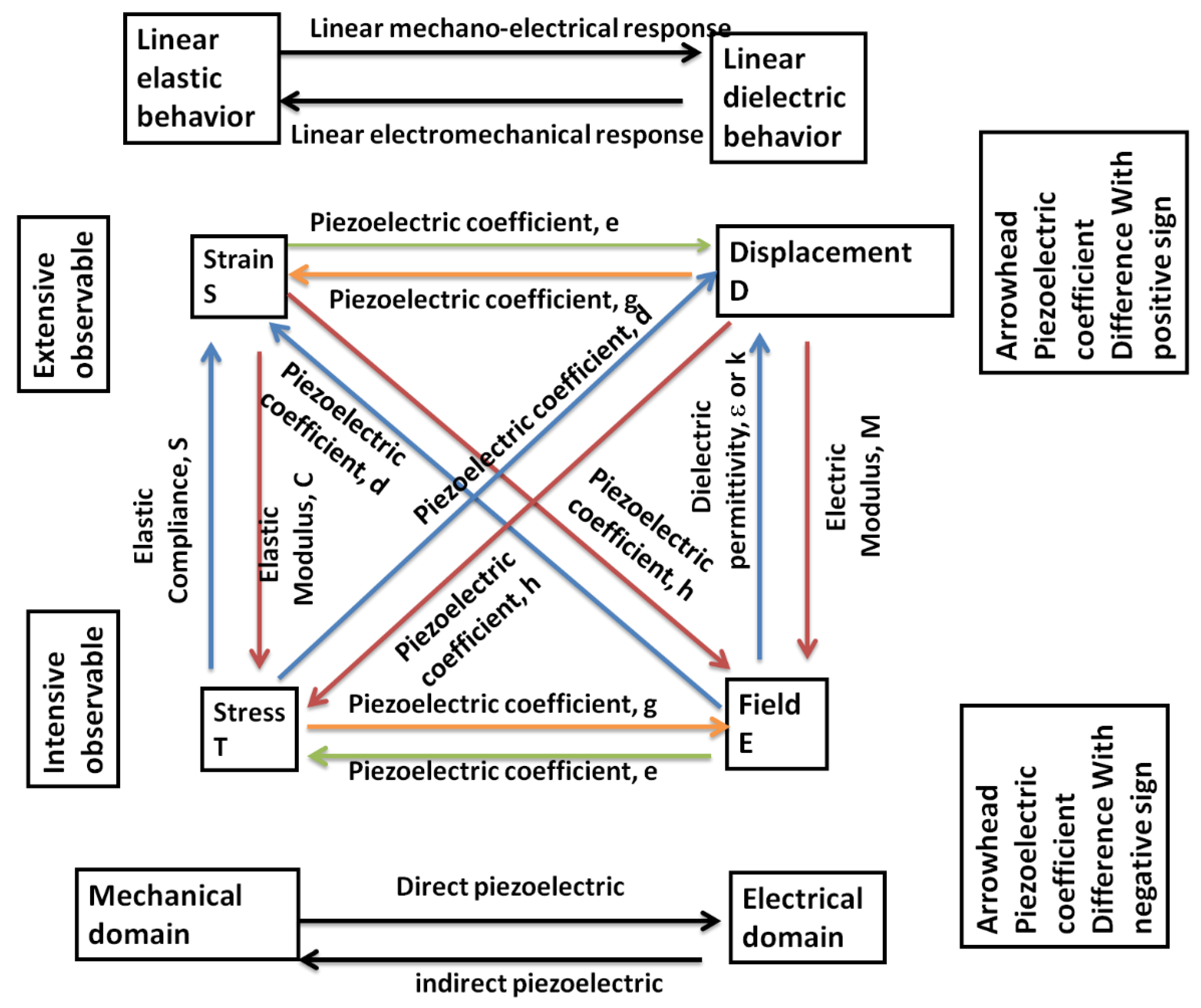
5. Nanometer Scale Domain Characterization
From the perspective of advanced materials characterization at nanoscale, developing and establishing nanometer scale domain characterization in line with the materials development would be of the first step unless materials properties become challenging to understand at the end because of the limit or lack of sensitive techniques with high detection limit and resolution. Moreover, understanding the origin and mechanisms of strain switching, compressive and tensile stress at nanoscale, absence or presence of inversion center, noncentrosymmetric and centrosymmetric properties, polarization switching, domain formation mechanisms, and polar order at surface, interface and wall, nanoscale structural characterization is necessary because of many controversies regarding the presence or absence of ferroelectricity in MAPbI3.[386] Therefore, it is pleased to organize nanoscale and advanced characterization tools for successful understanding of the halide perovskite field such as atomic force microscopy (AFM), piezoelectric force microscopy (PFM), photothermal induced resonance (PTIR), photoinduced force microscopy (PiFM), nonlinear optical spectroscopy, second harmonic generation (SHG) and theoretical or computational methods such as first principle calculations as discussed in detail in this sections and summarized in Scheme 11.
Scheme 11.
A representation of perovskite characterization methods and approaches.
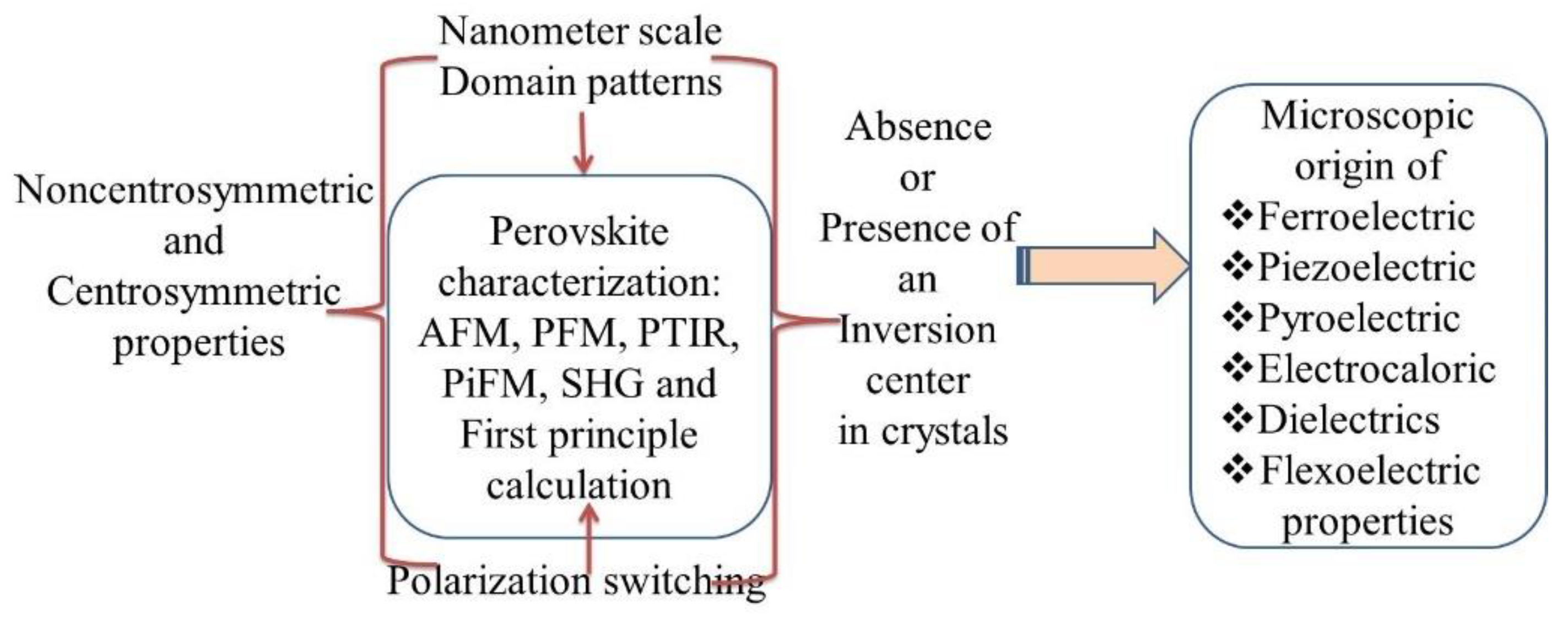
5.1. First-Principles Calculations
In parallel to the experimental perspectives, considering and understanding the theoretical perspectives and principles have vital contributions in designing and modeling of new materials, and predicting its properties with its functionalities. Numerous most important coming progresses in the sympathetic of ferroelectricity, piezoelectric and pyroelectrics need contributions from first-principles. Furthermore, there are very important concepts that first-principles studies can realize them: 1) the importance of hybridization. Contrasting the respected Slater rattling ion model,[387] the main element in oxide ferroelectrics is covalence or hybridization between the cation and its oxygen neighbors that lets the cation to travel off-center. This idea is at the present extensively applied in experiments and improvement of novel piezoelectric materials which it should be borrowed to the halide perovskite field. 2) the idea of polarization rotation, which is accountable for the huge electromechanical coupling seen in relaxor ferroelectrics like Pb(Mg1/3,Nb2/3)O6 (PMN)-PbTiO3 (PT).[388] 3) the association between cation ordering and polar nanoregions in relaxors.[389,390] 4) the guess of a morphotropic phase boundary in pure PT at high pressures with vast electromechanical coupling in the transition region.[391] 5) the discovery of reentrant ferroelectricity, with ferro-electricity regenerating at extremely high pressures, representing the option of entire novel lessons of ferroelectric materials.[392] Likewise, there are essential and more advanced concepts that should be addressed in hybrid perovskites using this method: (a), the role of large effective charges in electromechanical coupling, (b) sympathetic the function of hybridization and covalence in ferroelectric instability (c) the function of polarization rotation in the single crystal relaxor ferroelectrics, (d) the idea of polar ferroelectric superlatcies, (e) a primary sympathetic of macroscopic polarization, (f) plan paths for novel materials, and (g) an sympathetic of the necessities for materials to be multiferroics. Therefore, the movement and ordering of organic cations in halide perovskites is still controversial both theoretically[393,394,395,396]
Therefore, from the current theoretical perspective, the polarization intensity donated form the organic cations becomes predominantly controversial. For instance, Walsh et al.’s point out a spontaneous formation of ferroelectric domains in MAPbI3 and a huge polarization value of 38µC/cm2 has been demonstrated.[397] Another study showed that MA cations in tetragonal MAPbI3 have a special position along the c axis, and the polarization intensity is approximated to be 4.42 µC/cm2, which is mostly denoted by the MA dipole.[395] The authors also clarified that the large inconsistency from the Walsh’s study was perhaps because of the abandon of the relaxations or the possible inclusion of polarization quanta. From other research groups, the bulk polarization involvement solely from the organic molecular dipole moment is less than 2.5µC/cm2, and the PbI3 inorganic lattice has a main donation to the polarization.[398] Furthermore, their calculations demonstrated that the anti-ferroelectric tetragonal structure with almost zero net polarization is more stable than its ferroelectric complement by 21 meV, indicating that the ferroelectric domains cannot form spontaneously at room-temperature. Conversely, electronic structure has been calculated using first-principles to disclose a ferroelectric tetragonal structure with polarization of about 8 µC/cm2 above all denoted by the organic cations.[393]
5.2. Atomic force Microscopy
In order to investigate the microscopic origin of ferroelectric, piezoelectric and pyroelectric properties, AFM can associate the topography of a sample to other local material electrical characteristics, like conductivity and electrical potential.[208,399,400,401]This technique has been instrumental in ushering in the age of nanotechnology owing to its high resolution and sensitivity across a range of interaction forces, allowing AFM to find applications in materials science, physics, chemistry, and biology.[402] Initially developed to map surface topography of materials,[403] various modalities were subsequently developed to probe, e.g., mechanical, magnetic, electrical, and chemical properties.[404,405,406,407,408,409,410,411]
5.3. Photo Induced Force Microscope
This technique is still under growth, though previous models already able to extract quantitative information from PiFM images.[412,413] It is based on photoinduced forces between the sample and a sharp tip. A diagram of the interaction between the tip and the (nano) particle is shown by Figure 13a in which the system is light up via an inward light field E0. The condition in the tip−sample junction can be illustrated by estimating both the sample particle and the tip apex as polarizable spheres and bearing in mind only dipolar offerings.
Figure 13b shows an inverted optical microscope which applies an AFM detection head in place of a photodetector. The primary signal in PiFM is the time-integrated, photoinduced force as registered by the AFM head rather than detecting optical radiation. Furthermore, the light source in the PiFM system is a laser, which can be either a continuous wave (cw) of pulsed laser, relying on the type of optical experiment.
5.4. Visualizing Nanometer-Scale Domain Patterns
PFM is an instrument to set up polarization switching by visualizing nanometer-scale domain patterns[415,416,417,418,419,420] as well as nanoscale piezoelectricity and ferroelectricity.[421] Recently, the properties of 1D piezoelectric nanostructures were investigated with PFM.[422] This is an effective technique for drawing topography and conducting nondestructive property characterization of piezoelectric and ferroelectric materials at the nanoscale, giving convincing imminent keen on switching behavior and domain structures in single crystal and polycrystalline of MAPbI3. Nevertheless, it is recognized as it is disreputably sensitive to surface charging and ionic,[423] because it is applied in the electrochemical force microscopy.[424,425,426] Likewise, surface topography leads to strong topographic cross-talk,[427,428] which can give rise to recognition of step edges as ferroelectric domains or ferroelastic domains.[429] Thus, the surfaces of these materials are particularly unsteady in ambient environment seriously leading to the formation of the secondary phases like PbI2, etc. that can further facade intrinsic materials characters.[321,430,431] In similar way, it is possible that PFM is an AFM method based on the inverse piezoelectric effect that locally probe piezoelectric samples, visualize ferroic domains.[209,401]
5.5. Photothermal Induced Resonance
It computes the transient thermal expansion caused as a result of sample light absorption via contact mode AFM tip. This technique is also a composition sensitive scanning probe technique that unites the lateral resolution of AFM with the chemical exact of absorption spectroscopy.[432,433,434] In order to better illuminate, samples are light up from the underneath in an entire internal reflection design to reduce the interaction of light with the AFM tip as shown in Figure 14a. Additionally, the absorption of a laser pulse in the sample results in sample expansion, excitation of the AFM cantilever motion, and local heating, controlled by shinnying the AFM laser beam from the cantilever onto a four-quadrant photodetector (Figure 14a). Moreover, the ability for quantifying the chemical composition[435,436] with a spatial resolution down to 20 nm[434] has earned this technique considerable popularity for analyzing thin organic[437,438,439] or metal-organic materials.[436,440,441] However, because the PTIR signal is also proportional to the sample linear expansion coefficient, inorganic samples are typically challenging to measure. Furthermore, the thermal expansion is additional rapid compared to AFM response. It is sufficient to stimulate a number of the smallest-frequency mechanical modes of the cantilever (Figure 14c). The recurrence frequency of the laser pulses is sufficient to let the cantilever to finish the ring down (Figure 14b) prior to the latest pulse appears. Prominently, the PTIR signal is relative to the energy absorbed,[176]c and openly as good as with FT-IR spectral libraries[442,443] letting material recognition.
5.6. Differentiating Noncentrosymmetric and Centrosymmetric Crystals
Nonlinear optical spectroscopy is important to analyze films, which is an efficient and simple tool to differentiate between noncentrosymmetric and centrosymmetric crystals that indicate polar or nonpolar character of the crystal structure.
5.7. Identification of Inversion Center and Non-Centrosymmetry
The second-harmonic generation (SHG) is nonlinear optical technique developed to confirm absence or presence of an inversion center in crystals.[445,446] Since only non-centrosymmetric materials are SHG-active because of non-zero hyperpolarizability, β, it is also a sensitive tool for probing the loss of inversion symmetry in a phase transition. Furthermore, the molecular bottleneck for competent SHG functions are ruled by the necessity of insignificant absorption in the spectral region of attention and large first-order molecular hyperpolarizability (β).[447] Even though wide-ranging research has sketched a variety of issues for approximating, β,[448,449,450,451] the main building blocks for development of this ground is the translation of molecular non-linearity into a limited macroscopic second-order susceptibility (χ(2)), which demands crystallization into a non-centrosymmetric lattice. The total SHG intensity (I2ω) emitted by a sample calculated with the Kurtz-Perry method[452] shown in equation 28:
where Iω is the incident intensity, is an efficient susceptibility because of all dijk coefficients for which phase corresponding happens, depends on the dijk coefficients for which phase matching is not likely, and APM and ANPM are two functions that rely on the sample size, refractive indices, and particle size of the material for the wavelengths involved. If all dijk coefficients contribute to , then this parameter can be roughly estimated by dnorm.
5.8. Identification of the Polar Crystallographic Orientation
For investigation of a polar dielectric crystal, identification of the polar crystallographic orientation is required. Following powder X-ray diffraction of pulverized crystals, which confirmed the grown crystals to be MAPbI3, it is possible to determine the polar direction of a crystal, using specular diffraction from the surface of a single crystal.
6. New Application Trends beyond Photovoltaic
Piezoelectric energy harvesting devices are great solutions for a give application that requires high energy density, high voltage, little mechanical damping and high capacitance.[453] For this purpose halide perovskites have been tested as new energy harvesting piezoelectric materials.[454,455] This time, their wide range energy harvesting applications beyond photovoltaic become hot issue with great attention from the scientific community. In this section, we have presented piezoelectric energy harvesting, electromechanical and electronic energy conversion and storage device applications beyond photovoltaic, light emitting diode and laser applications, which are useful to the scientific community.
Halide peroveskite materials are widely researched for various applications such as photovoltaic, laser, light emitting diode, photocatalysis, etc. But, recently these materials become essential materials for energy harvesting applications such as self-powered unit, wireless electronics, storage devices, etc. as shown in Table 2.
6.1. Electrical Properties and Corresponding Applications
From the perspective of harvesting energy, it would be crucial to test halide perovskites for electronics functionalities beyond the photovoltaic, photonics or optical applications. In realization of these applications, the external stimuli which produce a corresponding application would also be better to consider. For instance, when a certain type of perovskite photovoltaic device is exposed to external stimulus such as light and thermal energies, the related processes are similar for different applications. In order not to present a generalized concept, we discussed the properties and applications[462] of several vital phase mixed-metal oxides based perovskite as shown in Table 3. The importance for these materials is in accordance of their intrinsic ferroelectric, piezoelectric, pyroelectric and dielectric properties of significance in related electronic applications such as field effect transistors, capacitors, transducers, high-k dielectrics, logic circuitry, actuators, dynamic random access memory, and electromechanical devices.[463,464,465] This is an excellent opportunity and great assignment for scientific communities in order to check whether halide perovskite materials can be used as alternative materials for the electronic applications described in the Table 2 or not. Above all, it would be of great concern whether the halide perovskite materials really own all the electronics properties stated in the Table 3 or not.
Note that the symbol ‘a’ indicates the proposed semiconducting properties and its corresponding applications are ‘not yet reported,’ which need future investigations.
As shown in Figure 15a, dielectric constant of CH3NH3PbI3 and Cl-MAPbI3 have been studied and found to be dependent on frequency.[108] The dielectric constant for CH3NH3PbI3 was ∼43 at 100 kHz. To understand the property of the dielectric constant, various amount of Cl was added and ∼90.9 was found for 4Cl-MAPbI3 sample but ∼62 for the 10Cl-MAPbI3 sample. This indicates that there should be an optimum value of Cl amount to obtain an optimum value of dielectric constant. Moreover, the value of the dissipation factor (D) for both CH3NH3PbI3 and Cl-MAPbI3 is shown in Figure15b and indicates that D increases with increasing amount of Cl. Furthermore, Figure15c shows dissipation factor and dielectric constant at 100 kHz as a function of the amount of MACl and MAI. Dense and smooth morphology of the sample film is suggested as possible cause for the larger dielectric constant obtained for Cl incorporated MAPbI3. To further understand what is happening with increasing amount of Br in which the dielectric constant get increased gradually. 6Br-MAPbI3 sample achieved ∼71.6 at 100 kHz. As shown in Figure15d-e, lower dissipation factor was observed owing to the incorporation of Br that results the formation of dense perovskite films. This incorporation of Cl and Br amounts shall create strain effect for the piezoelectric energy harvesting for effective power generation. Based on this concept, a compressive strain has been created generating output voltage of ∼0.78 V and output current density of ∼0.11 μA/cm2 from CH3NH3PbI3 and 2.75 V from 4Cl-MAPbI3 mixed peroveskite. The larger current density observed in Figure 15g shows that halide incorporation results the formation of surface morphologies which is denser and smoother. A P−E hysteresis loop is shown in Figure 15h and 0.56 μC/cm2 was obtained from 4Cl-MAPbI3. The increased polarization and dielectric constant is owing to the interfacial polarization caused by the coexistence of two phases such as MAPbCl3 and MAPbI3.[468,469] Such high leakage of current density and larger dielectric constant properties demonstrated by each sample are useful for high energy harvesting applications.
6.2. Structure Preference of Halide Perovskite Nanogenerators
From the perspective of device architecture or structure, understanding and developing the suitable hybrid perovskite nanogenerator device architecture in order to satisfy triple ‘E’ rule: efficient, economical and environmentally friendly would be of current and burning issue for scientific society. There are reports on peroveskite nanogeneratore that reflect halide perovskites are promising energy harvester for nanogenerator applications.[104,470] In recent times, a periodically release operations and vertical compression in the course of the piezoelectric structure has been reported as shown in Figure 16.[325] Moreover, halide controlled perovskites based nanogeneratore and capacitors are reported.[108,456] the reasons for high density powered nanogenerators is suggested as charging polarities,[481] soft elastic nature and soft polar optic phonons.[103] The operation of the nanogenerator is in either of the ways that Figure 16a shows that once electric dipoles are aligned in a single direction when vertical compression is used to the nanogenerator, the piezoelectric potential caused electrons move from the top electrode to the bottom electrode side through the external circuit. On the other way as demonstrated in Figure 16 the piezoelectric potential inside the device directly vanishes when the compressive is removed and the collected electrons from the bottom electrode flow back to the top electrode and an electric signal is shown in reverse direction. The intension here is not just to explain the operation but to point out the important concepts that motivate researchers to be curious on how to realize nanogenerator made of halide perovskites which satisfy the triple ‘E’ regulations.
More importantly, the concern of how to produce electrical energy from mechanical vibration is also a challenging lesson. Of these concerns considering beam structure as the most frequent solution to obtain electrical energy from mechanical vibrations has vital contribution. Accordingly, considering main factors such as generator structure, the generator size, electronic system of the control and storage of energy and piezoelectric material during the generation of effective electric energy using the piezoelectric generators has great importance. The most often tested piezoelectric generator structures are designs, in which the basic element, apart from the piezoelectric actuator, is the cantilever beam. One can single out a few possibilities of the connection of piezoelectric materials to the beam:
- beam made of the base material, with no piezoelectric properties, on which there is one (unimorph) or two piezoelectric material layers (bimorph). Generator with two plates of PZT ceramics (bimorph) is presented in Figure 17a,
- beam with an additional element influencing the increase of stresses in the piezoelectric material layers. An example of generator with one piezoelectric layer and an additional element is presented in Figure 17b,
- beam without piezoelectric material layers with the additional setup containing a piezoelectric material. An example of a generator of this type is presented in Figure 17c,
During beam bending, stresses appear in the piezoelectric material, on which electric charge builds up. An additional mass M installed at the end of the beam to increase stresses in the piezoelectric layers. Taking into consideration the fact that generators can power wireless sensors, generator structures should be small: about 1 cm3. It is to be noted that in generator structures based on cantilever beams and the PZT plates, the direction of external forces action is perpendicular to the direction of polarization. Hence, the piezoelectric coupling is indicated by the coefficient k31.[473] The increase of stresses in the piezoelectric element can be acquired by various beam shapes: most often a rectangle, but also a triangle[474], as well as by various geometry solutions of beam fixing to the object which is a source of vibration (Figure 18).
From the perspective of coupling modes for easy operations in line with the device architecture perspective, it would be of considering at least two frequently utilized coupling modes for piezoelectric power generators, recognized by the direction of the electric charge and mechanical force. Figure 19a illustrates the ‘33’ mode which indicates the charges accumulated on the electrode surface at right angles to the direction of polarization when compressive mechanical or tensile forces are applied in the axis of polarization. In similar way, Figure 19b shows the ‘31’ mode which indicates the charges accumulated on the electrode surface at right angles to the direction of polarization when a force is applied in the direction at right angles to the axis of polarization.[476] For most piezoelectric materials, the coupling factor of the 33-mode, k33, is larger than the coupling factor of 31-mode, k31 but it is not yet reported what this value is. In the 31-mode, the mechanical stresses are directed along the 1-axis. The stresses can be simply realized by bonding the piezoelectric element to a substructure experiencing bending while the 33-mode energy conversion can attain superior output power by increasing the layer of the ceramic (Stock type). For very low-pressure source and limited size, the 31-mode conversion may have a better benefit in energy conversion.[477] Because of the small size of the generator with the limited environmental sources for mechanical energy 31-mode energy conversion is appropriate for piezoelectric microgenerator applications in the micro-electromechanical systems (MEMS) structures.
6.3. Expected Piezoelectric Energy Conversion from Perovskite Materials
From the global direction and demand of energy conversion, there is a great concern and need to at least achieve enough energy or to also own extra or reserve energy. Another global concern is that which type of semiconducting materials can really satisfy the global energy demand in addition to the additional global concern of what kind of device architecture or structure to satisfy the triple ‘E’ rule as well as operating conditions discussed in the previous sections. Therefore, it is true to rise a great issue and concern of how much energy could be globally achieved from those energy harvesting semiconducting materials that everyone bears in his/her mind. Up to now, oxide based perovskite piezoelectric materials, along with the a number of energy conversion materials, are broadly applied for smart structures, generally categorized into two various kinds depending on the energy conversion route:[478] 1) The sensor type, wherein an electric charge is generated when a mechanical stress is used.; 2) the actuator type, where the piezoelectric element experiences a dimension variation when an electric field is utilized by which electric energy is changed into mechanical energy derived from the indirect piezoelectric effect. The field of potential applications of piezoelectric generators in energy harvesting systems is marked by the range of the electric power that can be generated by these generators. On the basis of published laboratory research results of piezoelectric generators one can state that the generated power does not excess several mW. The maximum power for selected piezoelectric generators with its dimensions is presented in Table 4.
According to the published research results three general factors influenced on the energy conversion efficiency can be enumerated: the greatest electric power is generated for a generator resonant frequency nearing to the driving frequency of the vibration source; the value of electrical power depends on a strain of piezoelectric material in the generator. Hence, generators with additional elements influencing on the increase of this strain generate more electrical power than typical cantilever beam generator; electrical power is proportional to a size of piezoelectric material used in generators.[482]
The performance of FAPbBr3-PDMS nanogenerator is approximately 0.44%[483,484,485,486] as shown in Table 5. An external compression cannot generate large strain on a piezoelectric FAPbBr3 nanoparticle because of the existence of PDMS matrix which bears the greater part of the compression.[487] Nevertheless, the hybrid composite piezoelectric nanogenerator can successfully avert the cracking and breaking of embedded piezoelectric nanoparticles under mechanical stress. Above all piezoelectric are smart for employ in large-scale piezoelectric energy harvesting, owing to their cost benefit, mechanical robustness, and easy device fabrication.[325]
6.4. Constructing Halide Perovskite Piezoelectric Dampers
It is clear that those inspiring devices are constructed from important materials with inspiring semiconducting, electrical, optical and structural properties. In order not to make general discussion we use PZT as example of those important materials with inspiring properties for inspiring applications. One of a fascinating function of PZT composites is to construct a passive mechanical damper as motivating concept to think the important question how to construct inspiring piezoelectric dampers from halide perovskites. For instance, taking the capacitance of the piezoelectric material as C and the vibration frequency as f with the series resistance as R, damping happen mainly quickly when the series resistor is chosen when the impedance corresponding condition, R=1/(2πfC), is fulfilled.[492] When a composite of piezoceramic powder, carbon black and polymer is fabricated (Figure 20a), the electrical conductivity of the composite is significantly altered using the addition of small amounts of carbon black (i.e., percolation effect).[493] A very interesting question to the halide perovskite community is that how these piezoelectric dampers can benefit from these low cost and materials simple to fabricate. Wondering that halide perovskite materials are not yet tested for this purpose although they were recently reported as materials which fulfill piezoelectric properties.
6.5. Constructing Halide Perovskite Piezoelectric Energy Harvesters
Wearable electronic devices[494] and wireless intelligent sensor network[495] have been recently grown quickly in areas such as medical science, energy, roads, bridges and military affairs. But, an essential trouble that needs to be considered is the energy delivered by these devices. Chemical batteries show a number of drawbacks, for example, large volume, inability to integrate with MEMS devices and short storage time with respect to the main energy. Also, their installation positions are not suitable for replacing the chemical batteries in case of a number of sensors. Consequently, the piezoelectric energy harvester that can acquire energy from the vibration environment is now a hot research topic as per the concern of an energy substitute for chemical batteries.[496,497,498] Moreover, the advantages of piezoelectric energy harvester includes: easy miniaturization, simple structure, no pollution, no electromagnetic interference and no fever in order to meet the energy need of low power consumption products. As a result, it is becoming vital choice of piezoelectric energy harvesting devices.
For constructing halide perovskite piezoelectric energy harvester, it is crucial to consider influencing parameters such as resonance voltage, structure type and resonance frequency in addition to the universal factors such as moisture. Researchers should consider the prevention mechanisms from moisture other environmental factors like the solar cell material prevention mechanisms listed elsewhere.[160] Hence, researching halide perovskite materials with low frequency piezoelectric energy harvesting capability are in great interest and are not yet tested for this purpose. With respect to the structure perspective, the piezoelectric energy harvester with a flexible cantilever beam becomes one of the major structural forms because of the concern of getting fast deformation response. For this structure, numerous correlated studies have been done, whether in the MEMS structure [499,500] or in the macro-structure .[501,502,503] Thus, there are two universal troubles for these accessible structures to be realized: the low power and output voltage, enforcing it challenging to be used and stored by the circuit rectifier, as well as the high frequency resonance frequency, which is complicated to harvest energy in the everyday environment. This will be of a great assignment for the halide perovskite community in order to confirm whether these materials can fill the listed two main challenges of the existing structures of piezoelectric energy harvester. Generally, piezoelectric energy harvesting devices are usually utilized in two modes: 33-Mode and 31-Mode. As Figure 20b-c displays, in 33-mode, the external stress direction and generates a voltage in the same direction, and in 31 mode, the applied stress is axial and perpendicular to the direction of the voltage generated.
6.6. A Self-Charging Power Unit and Wireless Electronic Applications
Recently, halide peroveskite materials particularly MA2SnX6[104] X = Cl, Br, and I and (CH(NH2)2SnBr3 (FASnBr3))[105] are used for powering self-charging power and wireless electronics. MA2SnCl6 perovskite demonstrated promising power density of 7.33 µW cm-2 for self-charging power unit. Similarly, FASnBr3 demonstrated high output power density 18.95 μW/cm2 for wireless electronics applications.[105] This indicates that self-powered Internet of Things devices built will be powered by halide perovskites in the near future. But, much effort for the development of this promising application is required. The current work is not well cultivated yet. Note that halide perovskites are not only useful for self-powered unit and wireless electronics but also may be useful for low power electronic devices to harvest waste heat because of their outstanding Pyroelectric and piezoelectric properties, and switchable polarization.
In order to understand the working mechanisms, Short-circuit I–t curves for self-powered ZPH photodetectors (PDs) was studied under wavelengths of 325 nm and 442 nm as shown in Figure21a.[358] This was aimed to understand the physical mechanisms of Pyroelectric effect together with photosensing and hence the Pyroelectric effect was detected at 325 nm (Figure 21a, b). Light-self-induced pyro-electric effect indicated by the short-circuit I–t curve under 325nm was divided in to I, II, III and IV (Figure 21b, c). It is easy to understand the physical mechanisms in these three stages. In Stage I, free carriers are generated in the form of photocurrent and distribution of polarization Pyroelectric charges due to temperature increase is achieved. In stage II, temperature becomes constant and illumination was retained because of which the Pyroelectric potential vanishes quickly owing to the presence of leakage, where a stable plateau was achieved by the output current(II, Figure 21b, c). In stage III, the pyro-potential distribution follows in the opposite direction to into stage ‘I’. This is caused by decrease in temperature directly, leading to current flows from FTO to Cu electrode. At this stage, thus, the photocurrent thus disappeared and similarly illumination is eliminated (III, Figure 21b, c). In Stage IV, the temperature becomes room temperature and get steady. The output returns to dark current and the pyro-potential disappears owing to leakage (IV, Figure 21b, c).
6.7. Nano-Plasmonic Sensing and Photoflexoelectric Effect
Nanostructured materials are highly essential in nanosensing applications owing to their stability, high sensitivity, selectivity, robust response, real time detection, and portability at nanoscale level.[504] The stimuli for such nanosensing are temperature, light, moisture, PH, etc. such nanosensors are electrical, electrochemical and chemical sensors useful for various detection applications.[505] Thus, materials with shape dependent chemical, electrochemical and physical properties and tunable size[506] are highly required. Moreover, sensitivity and selectivity of such sensing devices are highly useful parameters. The sensitivity of nanostructured material originates from its surface to volume ration while selectivity originates from surface functionalization and surface chemistry nature. The operational nanosensing mechanisms need great attention in any given nanostructured material for sensing purpose. The nanostructured material may be present in various forms such as nanowire, nanorod, nanotube, nano-sheet, etc. on the other hand; nano-plasmonic sensing is an alternative sensing platform, where geometries, various shapes and structural design are essential plasmonic properties are place of modification for various applications.[507] Moreover, nanoplasmonics is the study of electron oscillation in metallic nanoparticles and nanostructures, where surface plasmon has optical properties with the ability to confine light thereby monitoring light-matter interactions at the nanoscale.[508] Plasmon properties, for instance, resonance frequency and localization are monitored via nano-engineering the size, shape and composition of nanomaterial up on which monitoring plasmonic nanostructure properties is possible. Its main principle is that electron oscillation process where coherent electron oscillations called surface plasmon polaritons are travelling together with an electromagnetic wave along the interface between the dielectrics and the metallic nanostructure.[508] For this purpose, halide perovskites are applicable[509,510] owing to their tunable shape and composition dependent crystalline structure-properties,[505,511] and photosensing properties up on nano-engineering strategy.[358] The reason that halide perovskites are required in this discussion is owing to their extraordinary light-harvesting efficiency.[512,513,514,515] Furthermore, owing to their distinctive optical properties, large specific surface area, reduced stiffness and high electrical conductivity, nanoporous metal nanoparticles are plasmonic materials that may trigger halide perovskites to have potential for wide range applications such as photocatalysis, spectroscopy photovoltaic, energy harvesting, nanosensing and photoflexoelectric induced electromechanically systems.[516]
Not only nanosensing but also photoflexoelectric effect has been observed indicating that there is bending induced polarization in halide perovskites.[517] Such photoflexoelectric effect is caused by surface piezoelectricity, semiconductor barrier polarization, bulk flexoelectricity, flexoionics, or residual/ macroscopic piezoelectricity. This property is useful for photo-electromechanical multi-harvester and flexophotovoltaic applications. In the presence of dark and light, MAPbBr3 perovskite showed Bending-induced polarization as shown in Figure 22a. The “photoflexoelectric coefficient” of 10000% is observed and hence, this is the highest record. This coefficient is given in equ. 29
𝛾 ≡ (𝜇𝑙𝑖𝑔ℎ𝑡 – 𝜇𝑑𝑎𝑟𝑘)/𝜇𝑑𝑎𝑟𝑘
Under illumination, this coefficient goes higher and become independent of frequency at its saturation point but increase with light and strain as compared to flexoelectricity alone. Furthermore, the flexoelectric coefficient for various materials is shown in Figure 22b and thus, the highest coefficient is recorded for semiconductor photoflexoelectricity but the lowest is recorded for dielectric flexoelectricity.
This highest semiconductor photoflexoelectricity is obtained from MAPbBr3 in the presence of light. This record is promising for new potential application and research platform in the field of halide perovskites. Flexoelectricity or bending induced polarization is given by:[518] Ps = f (1/R1 + 1/R2), where Ps is polarization per unit area, f is flexoelectric coefficient, R1 and R2 are radius of bending material surface up on which a mechanical degree of freedom is produced. This is a direct flexoelectric effect the converse of which is trans-material voltage induced bending stress, given by: 2/Rm = fE (K + σ (r2/8). Rm is voltage induced bending, E = U/d =electric filed, U is material voltage and d is material thickness, K is bending elasticity of the material, σ is material tension and r is radius. Thus, photoflexoelectric effect is obtained from light, bending (curvature) and electricity. This flexoelectricity empowers piezoelectric effect that brings an abundant opportunity to actuation, energy harvesting and sensing applications.[519]
Moreover, strain gradient coupled with mechanical stress[519] and quantum tunneling[520] are responsible for the formation of bending induced polarization during which electromechanical coupling happens and hence is useful to characterize nano-scale flexoelectricity of nanostructured materials.[521] Such strain gradients are cause by lattice mismatch, spatial inhomogeneity of polarization and competing interfacial structures.[522] This effect is enabled by monitoring crystal structures symmetry and 4th rank tensor since it exists in all point groups i.e. it is the property of dielectrics, ferroelectric, semiconductors and others.[53] Recently, enabled using photo-mechanical coupling has been used for catalytic hydrogen production confirming wider application scope of photoflexoelectric effect.[523] Thus, such photoflexoelectric effect is not only the property of halide perovskites but also general property of semiconductors up on illumination generating photovoltaic transduction and electromechanical harvesting together.[517]
Plasmonic nanoparticle are quite essential to enhance the performance of nanosensors owing to their surface plasmon such as resonant optical scattering; local field enhancement and peculiar optical properties[507] from which free electrons are generated causing useful interactions between the active layers of a semiconductor and metallic nanostructures.[524] Recently, AuN@ CsPbBr3NCs@BaSO4, (MIP-PEG/CH3NH3PbI3 and CsPbBr3 QDs/RGO nano composites have been implemented for nanosensing applications.[505] Thus, the nano-plasmonic sensing for halide perovskites is not yet unleashed unlike for many sensing work progress as shown in the Table 6.
7. Big Challenges for Halide Perovskite Functionalization
Halide perovskites are widely known semiconducting materials with multifunctional properties. Current studies focused mainly on the studying energy harvesting multifunctional properties of these materials such as in nanogenerators, capacitors, self-powered unit, dampers and wireless electronics. However, ferroelectric instabilities, effect of impurity carrier and defects, surface and bulk effects as well as degradation and deformation influences on multifunctional properties of energy harvesting halide perovskites are not yet solved. In particular, the issues of stability and degradation may hinder the wide range of applications during energy harvesting. In this section we highlighted all these concerns to get great attention from the halide perovskite scientific communities and make them alert in this field. Magnetoelectric or electric control of magnetization and multiferroic properties are also essential in this field that must be clarified.[80,553]
7.1. Lattice Instability and Subtle Steadiness between the Short-Range Repulsions
Halide perovskites are normally narrow band gap semiconductor materials with exceptions that it ranges up to 3.1 eV for chloride perovskites. These semiconductors show lattice instability due to phase transition from cubic to orthorhombic crystal structures. However, it is not clear that whether lattice instability affects the ferroelectric properties of halide perovskites or not. Let us consider an effective Hamiltonian, Heff for ionic motion in the form that equation 30:
where the first and second terms are individually the kinetic and potential energies of the lattice of particle centers and E(Ri, Rj,...) is the commitment of the valence electrons by means of the electron-particle (or vibronic) interaction. The last is inferred in the adiabatic estimate which expect that valence electrons react basically promptly to a redistribution of ionic co-ordinates Ri, Rj,…
In the ensuing improvement of the essential model Hamiltonian a further critical supposition was made, to be specific that the electronic commitment E(Ri, Rj,...) to viable potential is autonomous of temperature. This estimate in this manner dismisses every single warm excitation of electrons from the valence to the conduction band and thus is equal to a supposition that the important band hole is extensive contrasted and warm energies. In this cutoff, or, in other words most ferroelectrics talked about to this point, the valence electrons assume just a detached role, in spite of the fact that the commitment E(Ri, Rj,...) to the resultant viable potential,
V(Ri, Rj,...) = U(Ri, Rj,...) + E(Ri, Rj,...) may in any case be fundamental for the adjustment of ferroelectricity in numerous materials. The principal term can be communicated in the ordinary route regarding ionic energy and uprooting co-ordinates. The aggregate free vitality currently takes the form that equation 31:
and can explain a ferroelectric instability if has a real solution, . From equation (34) by direct differentiation, we get equation 32,
As (high temperature) we find so that lattice distortion is absent. However, at the low-temperature extreme we find equation 33,
which is positive, representing a real value for when .
Obviously when this condition is fulfilled the low-temperature stable stage is ferroelectric while the high-temperature one is paraelectric. The ferroelectric insecurity is incited at a temperature Tc which, by putting in equation 31, can be computed in the form that equation 34,
and approaches zero as approaches solidarity from beneath. In the light of our presumptions concerning the type of the ionic free vitality this shakiness results exclusively from a vibronic coupling to the electronic movement. The more grounded the electron-phonon association parameter, the gentler the cross section (i.e. the littler ω2), and the littler the vitality band hole A, the less demanding the stage change can emerge.
Physically the change emerges as the aftereffect of a bringing down of the valence-band vitality by the electron-phonon association. In the event that the subsequent of a bringing down of electronic vitality is bigger than the potential vitality of the grid modes portraying the dynamic vibrations, at that point an unconstrained mutilation results. The presence of warm excitations between groups isn't basic to this instrument and for wide band holes, the ferroelectric unsteadiness in this model outcomes from the electronic potential term E(Ri, Rj . ..) instead of from the physically ionic potential U(Ri, Rj,.. ..). Specifically, the commitment E(Ri, Rj. . .) can be communicated expressly as far as the electron band and vibronic collaboration parameters, and subsequently the development coefficients of the subsequent aggregate compelling ionic potential V(Ri, Rj,...), prompting the potentials V and v, can be isolated into their physically electronic and ionic parts. On account of middle of the road or little band-hole circumstances, where electronic excitations are imperative, E(Ri, Rj,...) progresses toward becoming temperature subordinate and an enhancement of the fundamental model along the lines set out above ends up basic for a quantitative hypothetical investigation. Although the main cause for ferroelectric instability is not yet discovered fully, the expected cause is due to the subtle steadiness between the short-range repulsions preferring the non-polar paraelectric phase and long-range Coulomb forces preferring the polar ferroelectric phase. Thus, ferroelectric phase to occur, the phase transition has to be from non-polar paraelectric state into polar phase. Not only the coexistence of properties and the main cause for ferroelectric instability but also the effect of lone pairs present in Pb metal on ferroelectricity, polarity and conductivity of halide perovskite materials is not yet discovered.
7.2. The Influence of Nanoscale Defects
Ferroelectric materials are portrayed by an unconstrained polarization, which can be reoriented with a connected electric field. The switching between polarized domains is intervened by nanoscale defects. Thus, understanding the role of defects in ferroelectric switching is basic for down to earth applications, for example, non-volatile memories. This is particularly the situation for ferroelectric nanostructures and thin films in which the whole switching volume is proximate to an imperfect surface. Besides, these imperfections inside ferroelectric materials are by and large grouped into two non-fundamentally unrelated classes dependent on their impact on the free-vitality outline: Random-field defect and Random-bond defect. The first break the degeneracy of the polarization states to support at least one introductions and the second one change the barrier height for advances between worsen states. Interestingly, the most noticeable and voluminous defects in planar thin film heterostructures are the two interfaces, which break the precious crystal symmetry, as well as are joined by physical and synthetic recreations, bound charges, space charges and strain. These interfaces and deformities existing in the ferroelectric film decide the qualities of ferroelectric exchanging, despite the fact that not yet contemplated in halide perovskites. The impacts of the arbitrary field and irregular bond absconds are showed by changes in nucleation inclinations of the nearby exchanging under the surface test. In addition, the vital impacts of inhomogeneities, for example, impurities and radiation harm on the dielectric properties and switching conduct of ferroelectrics are of awesome enthusiasm since halide perovskites are delicate to radiations and light actuated recreations, heterogeneity and order-disorder.[163,361] For the most part, defects in any crystalline lattice cause twisting of the encompassing volume and change of the neighborhood fields. The sizes of these impacts are harder to assess than the impacts of domain walls since there are no 'mechanical-similarity' conditions and the degree of the precious crystal distortion relies upon the idea of the defect, its site in the crystal, and the host-imperfection association. In an acentric site an imperfection has a dipole minute related with it as shown in equation 35.
where is the difference in dipole minute at the deformity site and , is the relocation of charge qi in the encompassing lattice attributable to the nearness of the imperfection. In pyroelectrics and ferroelectrics reflects the polar idea of the host so the feeling of is the equivalent for every single comparative imperfection inside a solitary area. In the event that the deformity focus N is adequately weaken that the connection between them can be dismissed, the naturally visible polarization change is equation 36
which must now be included in the expression for the free energy of the ferroelectric.
For example, when the polarization of a gem is switched by a connected field, the polarization ΔP because of the imperfections could possibly turn around. If it reverses then the coercive field will rely upon both the field required to switch the imperfections and the sign and magnitude of ΔP. All in all the nearness of imperfections tends to expand the coercive field. In the event that ΔP does not turn around in an outer field the deformities can markedly affect the exchanging properties relying upon the dispersion of ΔP all through the gem volume. On the off chance that every one of the dipoles has a similar sense the hysteresis circles will seem one-sided as appeared in Figure 23a. On the off chance that the dipole introductions are requested over substantial locales, yet extraordinary districts are antiparallel similarly as ferroelectric domain, at that point the hysteresis circles could show up as in Figure 23b. On the off chance that the dipoles are totally irregular, as could occur in the event that they were brought into the crystal in a nonpolar phase, at that point the circle would seem typical with an expanded coercive field.
7.3. Surface and Bulk Effect
There have been a large number of trials which demonstrate that ferroelectric nature at the surfaces of precious crystals is not quite the same as the bulk nature. A portion of these observations have been made on as-developed precious crystals where the substance idea of the surfaces may not be all around described; for example the stoichiometry might be not the same as the bulk, or chemical adsorption may have happened.
7.4. Materials Degradation Effect
It is quite known that halide perovskites are sensitive to moisture, temperature, light and ambient atmosphere in general.[160] All these environmental factors cause degradation or at least materials deformation and property modifications resulting incorrect information. Thus, this subsection is to warrant the scientific community to carefully conduct their research considering all these factors. Recently, perovskite solar cell showed an excellent stability of 2143 hours of operation.[554] This is promising operational stability for solar cells. But, the key problem is material instability while working for other applications beyond photovoltaic.
8. Concluding Remark
Halide perovskites have emerged as a promising material for application in solar cells and other potential optoelectronic devices beyond photovoltaic due to their unique optoelectronic properties. As a result of their uniqueness, perovskite solar cells demonstrated an appreciable development in PCE, beyond 29%. In spite of the appreciable development, fundamental sympathetic of the device photophysics is not yet realized. Moreover, understanding of the major applications beyond photovoltaic and their microscopic origin and mechanisms of multifunctional properties, growing energy harvesting, nano-sensing and photoflexoelectric performances imparts great consideration. Furthermore, new electronic applications such as piezoelectric nanogenerator, piezoelectric dampers, self-powered unit and electromechanical devices are promising research topics in halide perovskites materials nano-engineering research and cross-disciplinary energy materials research. Besides, the existence of a switchable spontaneous electric polarization creates piezoelectric and pyroelectric responses for utilizing in a lot of functions such as energy harvesting, photoflexoelectricity and nano-plasmonic sensing devices and thermoelectric applications. Therefore, developing general nano-engineering strategy for designing new energy harvesting, sensing and electromechanical response is important and should get special attentions. In addition to this, it is vital to understand the piezoelectric properties of halide perovskite materials. In particular, enhancement of piezoelectric properties, piezoelectric applications as well as the suitability of its structure for reliable applications and efficient piezoelectric energy conversion are applicable research questions this time. It is also still vital to know whether the symmetry of these materials is an important issue that should be considered during the study of their electronics properties and related applications or not. Furthermore, identifying the factors and issues influencing the clear understanding of these electrical parameters would be of future primary task in this field of halide perovskite study. In conclusion, we proposed new research direction for the development of halide perovskites research in focusing on the nano-engineering of polar order, strain, surface, domain and interface as well as thermodynamic concepts. In order to confirm whether halide perovskite materials own all these electrical properties or not, developing advanced characterization spectroscopic techniques is highly relevant. Especially, nanometer scale domain characterization tools such as AFM, PFM, PTIR, PiFM, nonlinear optical spectroscopy, SHG and first principle calculation impart the great interest for this purpose. In this review, possible energy harvesting, sensing and electromechanical response of halide perovskites applications beyond photovoltaic are reviewed and big challenges for halide perovskite functionalization are highlighted to guide industries and research institutions.
Contributions
All the authors contributed to the research, results analysis, and manuscript.
Data availability
All data are inserted in the body of the manuscript
Acknowledgement
This work was financially supported by the Ministry of Science and Technology (MoST) (106-2923-E 011-005, 105-3113-E-011-001, 105-ET-E-011-004-ET, 104-2923-M-011-002-MY3, 104-2911-1-011-505-MY2, 103-2221-E-011-156-MY3), the Top University Projects (100H45140), the Global Networking Talent 3.0 Plan (NTUST 104DI005) from the Ministry of Education of Taiwan, Taiwan’s Deep Decarbonization Pathways toward a Sustainable Society Project (106-0210-02-11-03) from Academia Sinica as well as the facilities of support from Adigrat University, National Taiwan University of Science and Technology (NTUST) and National Synchrotron Radiation Research Centre (NSRRC) are also acknowledged.
Competing Interests
The authors declare no conflict of interest.
References
- A. Al-Ashouri, E. Köhnen, B. Li, A. Magomedov, H. Hempel, P. Caprioglio, J. A. Márquez, A. B. Morales Vilches, E. Kasparavicius, J. A. Smith, N. Phung, D. Menzel, M. Grischek, L. Kegelmann, D. Skroblin, C. Gollwitzer, T. Malinauskas, M. Jošt, G. Matič, B. Rech, R. Schlatmann, M. Topič, L. Korte, A. Abate, B. Stannowski, D. Neher, M. Stolterfoht, T. Unold, V. Getautis and S. Albrecht, Science, 2020, 370, 1300-1309.
- Y. Y. a. S. Y. e. a. Xiao Z, Nat Mater, 2015, 14, 193–198.
- A. Richter, M. Hermle and S. W. Glunz, IEEE Journal of Photovoltaics, 2013, 3, 1184-1191.
- L. Jonathan, L. J. Diguna, O. Samy, M. Muqoyyanah, S. Abu Bakar, M. D. Birowosuto and A. El Moutaouakil, Polymers, 2022, 14, 1059.
- J. H. S. DeWolf, S.-J. Moon, P. Löper, B. Niesen, M. Ledinsky, F.-J. Haug, J.-H. Yum, and C. Ballif,, J. Phys. Chem. Lett., 2014, 5, 1035.
- Y. Y. Y. Yang, M. Yang, S. Choi, K. Zhu, J. M. Luther, and M. C. Beard, , Nat. Commun., 2015, 6, 7961.
- A. M. A. Miyata, P. Plochocka, O. Portugall, J. T.-W.Wang, S. D. Stranks, H. J. Snaith, and R. J. Nicholas, , Nat. Phys., 2015, 11, 582.
- G. E. E. C. Wehrenfennig, M. B. Johnston, H. J. Snaith, and L. M. Herz, , Adv. Mater., 2014, 26, 1584.
- K. T. B. J. M. Frost, F. Brivio, C. H. Hendon, M. van Schilfgaarde, and A. Walsh, , Nano Letters, 2014, 14, 2584.
- F. Z. S. Liu, I. Grinberg, and A. M. Rappe, , Journal of Physical Chemistry Letters 2016, 7, 1460.
- A. G. M. Coll, E. M. Marza, O. Almora, G. G. Belmonte, M. C. Quiles, J. Bisquert, , J. Phys. Chem. Lett., 2015, 6, 1408.
- G. S. H. D. Seol, C. Bae, H. Shin, H. S. Jung, and Y. Kim, , Journal of Materials Chemistry A, 2015, 3, 20352.
- J. F. S. Q. F. Dong, Y. J. Fang, Y. C. Shao, S. Ducharme, and J. S. Huang, , Advanced Materials,, 2016, 28, 2816.
- H. L. R. Ding, X. Zhang, J. Xiao, R. Kishor, H. Sun, B. Zhu, G. Chen, F. Gao, X. Feng, J. Chen, X. Chen, X. Sun, and Y. Zheng, , Advanced Functional Materials, 2016, 26, 7708.
- T.-V. D. Y.-J. Kim, H.-J. Choi, B.-J. Park, J.-H. Eom, H.-A. Song, D. Seol, Y. Kim, S.-H. Shin, J. Nah, and S.-G. Yoon,, Journal of Materials Chemistry A 2016, 4, 756.
- Q. D. E. Strelcov, T. Li, J. Chae, Y. Shao, Y. Deng, A. Gruveman, J. Huang, and A. Centrone, , , Sci. Adv. accepted, 2016.
- B. Huang, Z. Liu, C. Wu, Y. Zhang, J. Zhao, X. Wang and J. Li, National Science Review, 2021, 8.
- L. Y. Y. Zhou, S. W. Wang, Z. L. Ku, H. J. Fan, D. Schmidt, A. Rusydi, L. Chang, L. Wang, P. Ren, L. F. Chen, G. L. Yuan, L. Chen, and J. L. Wang, , Nat Commun, 2016, 7.
- K. T. B. J. M. Frost, A. Walsh,, APL Mater., 2014, 2, 081506.
- F. Z. S. Liu, N. Z. Koocher, H. Takenaka, F. Wang, and A. M. Rappe,, J. Phys. Chem. Lett., 2015, 6, 693.
- D. A. E. T. M. Brenner, L. Kronik, G. Hodes, and D. Cahen, , Nat. Rev. Mater., 2016, 1, 15007.
- D. Li, H. Wu, H. C. Cheng, G. Wang, Y. Huang and X. Duan, ACS Nano, 2016, 10, 6933-6941.
- R. Singh and M. Parashar, in Soft-Matter Thin Film Solar Cells: Physical Processes and Device Simulation, eds. J. Ren and Z. Kan, AIP Publishing LLC, p. 0. [CrossRef]
- K.-G. L. Hobeom Kim† , Tae-Woo Lee*, Energy Environ. Sci., 2015, 00, 1-3.
- D. H. S. Jin Hyuck Heo , Hye Ji Han , Seong Yeon Kim , Jun Ho Kim , Dasom Kim , Hee Won Shin , Tae Kyu Ahn , Christoph Wolf , Tae-Woo Lee , and Sang Hyuk Im* Adv. Mater. , 2015.
- S. I. Ryotaro Inoue, Ryota Imura, Yuuki Kitanaka, Takeshi Oguchi, Yuji Noguchi & Masaru Miyayama, Scientific RepoRts, 2015, 5, 14741.
- a. D. K. Hyeon Han, a Sangmin Chae,b Jucheol Park,c Sang Yeol Nam,c,d Mingi Choi,e Kijung Yong,e Hyo Jung Kim,b Junwoo Son,*a and Hyun Myung Jang*a, Nanoscale, 2018.
- F. Z. Lu You1*, Liang Fang3*, Yang Zhou1, Liang Z. Tan2, Zeyu Zhang4, Guohong Ma4, Daniel Schmidt5‡, Andrivo Rusydi5, Le Wang1§, Lei Chang1, Andrew M. Rappe2¶, Junling Wang1¶, Sci. Adv., 2018, 4.
- a. J. S. Bo Chen, b Xiaojia Zheng,*a Yuan Zhou,a Kai Zhu,c Shashank Priya*a, J. Mater. Chem. A, 2015. [CrossRef]
- X. S. Jingjiao Zhang1, Mingrong Shen1, Zhihua Dai1, Lingjun Zhang1, Xiyun He2, Wenxiu Cheng2, Mengyu Cao1 & Guifu Zou1, Scientific Reports, 3, 2109.
- I. B. W. Padinhare Cholakkal Harikesh, Biplab Ghosh, Rohit Abraham John, Stener Lie, Krishnamoorthy Thirumal, Lydia Helena Wong, Tze Chien Sum, Subodh Mhaisalkar, and Nripan Mathews*, Adv. Mater., 2018, 1802080.
- C. R. V. Fridkin, 2001, 46, 654-658.
- V. 18 L. Pintilie, G. Le Rhun and M. Alexe, , J. Appl. Phys., , 2007, 101, 064109.
- J. Oh, Yuan, H. C. & Branz, H. M. , Nat. Nanotechnol., 2012, 7, 743-748.
- B. G. t. O’Regan, M. , Nature , , 1991, 353, 737-740.
- S. R. Wenham, Green, M. A., Watt, M. E. & Corkish, R. , Earthscan Ltd, , 2006.
- D. G. McGehee, Nature Photonics, 2009, 3, 250-252.
- H. S. Nalwa, American Scientific Publishers, 2008.
- a. J. S. Bo Chen, b Xiaojia Zheng,*a Yuan Zhou,a Kai Zhu,c Shashank Priya*a, J. Mater. Chem. A 2012, 00, 1-3.
- B. Chen, J. Shi, X. Zheng, Y. Zhou, K. Zhu and S. Priya, Journal of Materials Chemistry A, 2015, 3, 7699-7705.
- S. M. Young, F. Zheng and A. M. Rappe, Phys. Rev. Lett., 2012, 109, 236601.
- F. Z. S. M. Young, A. M. Rappe, , Phys. Rev. Lett., 2012, 109, 236601.
- V. D. L. A. M. Glass, T. J. Negran, Appl. Phys. Lett., 1974, 25, 233.
- J. S. S. Y. Yang, S. J. Byrnes, P. Shafer, C.-H. Yang, M. D. Rossell, P. Yu, Y.-H. Chu, J. F. Scott, J. W. Ager III, L. W. Martin, R. Ramesh, , Nat. Nanotechnol., 2010, 5, 143-147.
- A. R. C. A. Bhatnagar, Y. H. Kim, D. Hesse, M. Alexe, , Nat. Commun., 2013, 4, 2835.
- H. Y. L. Ye, W. Q.; Hu, C. L.; Zhang, Y.; You, Y. M.; Mao, J. G.; Li, P. F.; Xiong, R. G. , Adv. Mater. , 2016, 28 (13), 2579−2586.
- H.-Y. W. Zhang, Z.; Li, P.-F.; Tang, Y.-Y.; Liao, W.-Q.; Ye, H.-Y.; Cai, H.; Xiong, R.-G. , Angew. Chem., Int. Ed. , 2018 57 (2), 526−530.
- W. T. a. H. B. e. a. Ahmadi M, AdvMater 2017, 29, 1605242.
- Evgheni Strelcov, 2* Qingfeng Dong,3* Tao Li,4* Jungseok Chae,1,2*†‡ Yuchuan Shao,3,4 Yehao Deng,3,4 Alexei Gruverman,4§ Jinsong Huang,3§ Andrea Centrone1§ Sci. Adv., 2017, 3, e1602165.
- G. R. Gou, J. M. , Adv. Mater. Interfaces, 2014, 1, 1400042.
- M. B. Yuheng Li, Joseph Wong, and Kesong Yang, J. Phys. Chem. C,, 2017.
- Y. Chen, Y. Lei, Y. Li, Y. Yu, J. Cai, M.-H. Chiu, R. Rao, Y. Gu, C. Wang, W. Choi, H. Hu, C. Wang, Y. Li, J. Song, J. Zhang, B. Qi, M. Lin, Z. Zhang, A. E. Islam, B. Maruyama, S. Dayeh, L.-J. Li, K. Yang, Y.-H. Lo and S. Xu, Nature, 2020, 577, 209-215.
- R. A. Surmenev and M. A. Surmeneva, Materials Today, 2023, 67, 256-298.
- B. Yang, D. Bogachuk, J. Suo, L. Wagner, H. Kim, J. Lim, A. Hinsch, G. Boschloo, M. Nazeeruddin and A. Hagfeldt, Chemical Society Reviews, 2022. [CrossRef]
- S. B. Nazir, M.; Yang, K. , Appl. Phys. Lett., 2014, 105, 141602-141605.
- K. S. Yang, W.; Wang, S.; Nardelli, M. B.; Curtarolo, S. , Nat. Mater., 2012, 11, 614-619.
- M.-J. Choi, J. W. Lee and H. Jang, Advanced materials (Deerfield Beach, Fla.), 2023, e2308827. [CrossRef]
- Y. D. Jingjing Zhao, 1 Haotong Wei,1 Xiaopeng Zheng,1 Zhenhua Yu,1 Yuchuan Shao,1 Jeffrey E. Shield,1 Jinsong Huang1,2*, Sci. Adv. , 2017, 3, eaao5616.
- D. B. Kim, J. Y. Kim, J. Han and Y. S. Cho, Nano Energy, 2024, 125, 109551.
- N. Muralidharan, R. Carter, L. Oakes, A. P. Cohn and C. L. Pint, Scientific Reports, 2016, 6, 27542.
- S. S. Won, H. Seo, M. Kawahara, S. Glinsek, J. Lee, Y. Kim, C. K. Jeong, A. I. Kingon and S.-H. Kim, Nano Energy, 2019, 55, 182-192.
- M.-J. Choi, J.-W. Lee and H. W. Jang, Advanced Materials, 2024, 36, 2308827.
- D. Liu, D. Luo, A. N. Iqbal, K. W. P. Orr, T. A. S. Doherty, Z.-H. Lu, S. D. Stranks and W. Zhang, Nature Materials, 2021, 20, 1337-1346.
- W. Meng, K. Zhang, A. Osvet, J. Zhang, W. Gruber, K. Forberich, B. Meyer, W. Heiss, T. Unruh, N. Li and C. J. Brabec, Joule, 2022, 6, 458-475.
- J. Liu, M. P. Garman, J. Dong, B. van der Zee, L. Qiu, G. Portale, J. C. Hummelen and L. J. A. Koster, ACS Applied Energy Materials, 2019, 2, 6664-6671.
- X. Yu, Y. Hou, M. Zheng, J. Yan, W. Jia and M. Zhu, Journal of the American Ceramic Society, 2019, 102, 275-284.
- Y. Zhong, Y.-E. Huang, T. Deng, Y.-T. Lin, X.-Y. Huang, Z.-H. Deng and K.-Z. Du, Inorg. Chem., 2021, 60, 17357-17363.
- E. Arkan, A. Karabiber, M. A. Topçu, Z. Kinas, A. Sarilmaz, S. S. Ozel and F. Ozel, Surfaces and Interfaces, 2023, 37, 102683.
- M. Martín-González, O. Caballero-Calero and P. Díaz-Chao, Renewable and Sustainable Energy Reviews, 2013, 24, 288-305.
- X. Yu, L. Zhu, X. Li, J. Zhao, T. Wu, W. Yu and W. Li, Materials, 2023, 16, 1778.
- W. Yao, L. Shen, P. Liu, C. Liu, J. Xu, Q. Jiang, G. Liu, G. Nie and F. Jiang, Materials Chemistry Frontiers, 2020, 4, 597-604.
- N. K. Sinha, P. Roy, D. S. Ghosh and A. Khare, Materials Today: Proceedings, 2023, 83, 6-13.
- S. Jiang, M. Liu, D. Zhao, Y. Guo, J. Fu, Y. Lei, Y. Zhang and Z. Zheng, Physical Chemistry Chemical Physics, 2024, 26, 4794-4811.
- C. He, J. Qiu, Z. Mu and X. Liu, CCS Chemistry, 2023, 5, 1961-1972.
- Y. Lin, Y. Zhong, Y. Lin, J. Lin, L. Pang, Z. Zhang, Y. Zhao, X.-Y. Huang and K.-Z. Du, Frontiers of Optoelectronics, 2024, 17, 6.
- T. J. C.-B. Jacobsson, J.-P.; Pazoki, M.; Saliba, M.; Schenk, K.; Gratzel, M.; Hagfeldt, A. , Energy Environ. Sci., 2016, 9, 1706-1724.
- W.-L. L. Yan, G.-H.; Liu, F. , J. Phys. Chem. C , , , 2016, 120, 17972-17977.
- L. V. Atourki, E.; Mar , B.; Mollar, M.; Ahsaine, H. A.; Bouabid, K.; Ihlal, A. , Appl. Sur. Sci., 2016, 371.
- D. S. D. a. B. P. e. a. Stroppa A, Nat Commun 2014, 5 5900.
- J. P. a. B. P. e. a. Stroppa A, Angew Chem, 2011, 123, 5969–5972.
- B. P. a. J. P. e. a. Stroppa A, Adv Mater 2013, 25, 2284–2290.
- S. A. a. J. P. e. a. Di Sante D, J Am Chem Soc 2013, 135, 18126–18130.
- S. Bhatti, C. Ma, X. Liu and S. N. Piramanayagam, IEEE Transactions on Magnetics, 2019, PP.
- S. Pruvost, A. Hajjaji, L. Lebrun, D. Guyomar and Y. Boughaleb, The Journal of Physical Chemistry C, 2010, 114, 20629-20635.
- A. R. Balakrishna and J. E. Huber, Smart Materials and Structures, 2016, 25, 104001.
- S. K. b. Wei-Jian Xu a, Andrei Kholkin b,c,⇑, João Rocha a, Coordination Chemistry Reviews, 2019, 387, 398–414.
- K. S. a. K. A. e. a. Xu WJ, Coord Chem Rev 2019, 387 398–414.
- T. R. S. S.-E. Park, J. Appl. Phys., 1997, 82, 1804-1811.
- D. G. S. J. Mannhart, Science, 2010, 327, 1607-1611.
- Y. I. H. Y. Hwang, M. Kawasaki, B. Keimer, N. Nagaosa, Y. Tokura, , Nat. Mater., 2012, 11, 103-113.
- C. M. B. J. A. Mundy, M. E. Holtz, J. A. Moyer, H. Das, A. F. Rébola, J. T. Heron, J. D. Clarkson, S. M. Disseler, Z. Liu, A. Farhan, R. Held, R. Hovden, E. Padgett, Q. Mao, H. Paik, R. Misra, L. F. Kourkoutis, E. Arenholz, A. Scholl, J. A. Borchers, W. D. and R. R. Ratcliff, C. J. Fennie, P. Schiffer, D. A. Muller, D. G. Schlom, Nature, 2016, 537, 523-527.
- J.-M. L. S. Dong, S.-W. Cheong, Z. Ren, , Adv. Phys., 2015, 64, 519-626.
- D. V. M. Stengel, N. A. Spaldin, Nat. Mater., 2009, 8, 392-397.
- M. D. E. Bousquet, N. Stucki, C. Lichtensteiger, P. Hermet, S. Gariglio, J. M. Triscone, P. Ghosez, Nature, 2008, 452, 732-736.
- Y. L. Z. Y. L. Tang, X. L. Ma, A. Y. Borisevich, A. N. Morozovska, E. A. Eliseev, W. Y. Wang, Y. J. Wang, Y. B. Xu, Z. D. Zhang, S. J. Pennycook, , Science 2015, 348, 547-551.
- Y. Y. Kutes, L.; Zhou, Y.; Pang, S.; Huey, B. D.; Padture, N. P, J. Phys. Chem. Lett., 2014, 5, 3335−3339.
- F. Z. Shi Liu, Nathan Z. Koocher, Hiroyuki Takenaka, Fenggong Wang, and Andrew M. Rappe*, J. Phys. Chem. Lett. , 2015, 6, 693−699.
- Z. C. Deyang Chen, Qian He, James D. Clarkson, Claudy R. Serrao, Ajay K. Yadav, Mark E Nowakowski, Zhen Fan, Long You, Xingsen Gao, Dechang Zeng, Lang Chen, Albina Y. Borisevich, Sayeef Salahuddin, Jun-Ming Liu, and Jeffrey Bokor, Nano Lett., 2016.
- G. Arlt, J. Mat. Sci. , 1990, 25, 2655--2666.
- R. E. Newnham, Springer-Verlag, Berlin, 1975.
- W. R. Cook, J. Am. Ceram. Soc., 1956, 39, 17-19.
- Y. e. a. Kutes, J. Phys. Chem. Lett., 2014, 5, 3335−3339.
- R. Pandey, G. Sb, S. Grover, S. K. Singh, A. Kadam, S. Ogale, U. V. Waghmare, V. R. Rao and D. Kabra, ACS Energy Lett, 2019, 4, 1004-1011.
- S. Ippili, J. H. Kim, V. Jella, S. Behera, V.-H. Vuong, J.-S. Jung, Y. Cho, J. Ahn, I.-D. Kim, Y. H. Chang, H.-S. Kim and S.-G. Yoon, Nano Energy, 2023, 107, 108148.
- M. M. Rana, A. A. Khan, W. Zhu, M. F. A. Fattah, S. Kokilathasan, S. Rassel, R. Bernard, S. Ababou-Girard, P. Turban, S. Xu, C. Wang and D. Ban, Nano Energy, 2022, 101, 107631.
- Tie Zhang1, †, Ke Xu1,†, Jie Li1, Lei He 1, Da-Wei Fu2,∗, Qiong Ye1,∗ and Ren-Gen Xiong 1,∗, Natl Sci Rev 2023,, 10, nwac240.
- Z. H. a. C. X. e. a. Liu HY, J Am Chem Soc 2020, 142, 15205–15218.
- V. Jella, S. Ippili and S.-G. Yoon, ACS Applied Electronic Materials, 2020, 2, 2579-2590.
- L. F. a. B. S. e. a. Breternitz J, AngewChem Int Ed 2020, 59 424–428.
- Peng Gao1, Heng-Jui Liu3, Yen-Lin Huang3, Ying-Hao Chu3,4, Ryo Ishikawa5, Bin Feng5, Ying Jiang2,6, Naoya Shibata5, En-Ge Wang2,6 & Yuichi Ikuhara5,7,8, Nat. Commun., 2016, 7, 11318.
- L. K. a. L. Z. G. e. a. An LC, Small, 2021, 17.
- T. Y. a. L. P. e. a. Liao WQ, J Am Chem Soc 2018, 140, 3975–3980.
- M. S. Bokdam, T.; Stroppa, A.; Picozzi, S.; Sarma, D. D.; Franchini, C.; Kresse, G., , Sci. Rep., 2016, 6, 28618.
- Jia-Bin Li1, 3,7, Zhi-Kang Jiang1,2,7, Rui Wang 4,5,6, Jin-Zhu Zhao 1,2,6✉ and Ruiqiang Wang1,2✉, npj Computational Materials 2023, 9, 62.
- J. H. N. N.J. Jeon, W.S. Yang, Y.C. Kim, S. Ryu, J. Seo, S.I. Seok, , Nature, 2015, 517, 476-480.
- F. Igbari, R. Wang, Z.-K. Wang, X.-J. Ma, Q. Wang, K.-L. Wang, Y. Zhang, L.-S. Liao and Y. Yang, Nano Letters, 2019, 19, 2066-2073.
- J. Zhou, Z. Xia, M. S. Molokeev, X. Zhang, D. Peng and Q. Liu, Journal of Materials Chemistry A, 2017, 5, 15031-15037.
- K. A. Bush, K. Frohna, R. Prasanna, R. E. Beal, T. Leijtens, S. A. Swifter and M. D. McGehee, ACS Energy Lett, 2018, 3, 428-435.
- E. T. M. Matthew R. Linaburg, Jackson D. Majher, and Patrick M. Woodward*, Chem. Mater., 2017, 29, 3507−3514.
- M. B. Gray, E. T. McClure and P. M. Woodward, Journal of Materials Chemistry C, 2019, 7, 9686-9689.
- Y. e. a. Liu, Nat. Mater. , 2018, 17, 1013–1019.
- S. H. B. D. Lee, T. H. Kim, J.-G. Yoon, C. M. Folkman, C. B. Eom, T. W. Noh, , Phys. Rev., 2011, B 84, 125305.
- G. L. a. G. a. Chen C, Nat Commun 2019, 10.
- T. K. a. M. H. e. a. Huang PJ, J Am Chem Soc 2019, 141, 14520–14523.
- J. P. Even, L.; Jancu, J.-M.; Katan, C.,, J. Phys. Chem. Lett., 2013, 4, 2999-3005.
- E. T. B. Fedwa El-Mellouhi1, Asma Marzouk1, Sergey N Rashkeev1, Sabre Kais1,2,3 and Fahhad H Alharbi1,2, npj Computational Materials 2016, 16035.
- G. K. a. P. M. Woodward*, J. Mater. Chem., 2010, 20, 5785-5796.
- G. P. a. B. P. Uberuaga, JOURNAL OF APPLIED PHYSICS , , 2015, 117, 114103.
- A. M. Amat, E.; Ronca, E.; Quarti, C.; Umari, P.;Nazeeruddin, M. K.; Grätzel, M.; De Angelis, F. , Nano Lett., 2014, 14, 3608−3616.
- H. K. Jongseob Kim1, Mahesh Chandran3, Seung-Cheol Lee3,a), Sang Hyuk Im4, and Ki-Ha Hong5,b), APL Materials, 2018, 6, 084903.
- F. D. a. S. N. e. a. Passarelli JV, J Am Chem Soc 2018, 140, 7313–7323.
- B. S. Chen, J.; Zheng, X.; Zhou, Y.; Zhu, K.; Priya, S., , J. Mater. Chem. A, 2015, 3, 7699-7705.
- M. N. a. E. J. Katan C, Chem Rev 2019, 119, 3140–3192.
- S. X. a. Z. Z. e. a. Chen XG, J Am Chem Soc 2020 142, 10212–10218.
- M. G. Mączka, A.; Ptak, M.; Paraguassu, W.; da Silva, T. A.; Sieradzki, A.; Pikul, A. , Chem. Mater., 2017, 29 (5), 2264−2275.
- M. P. Mączka, M.; Gągor, A.; Stefańska, D.; Sieradzki, A. , Chem. Mater., 2019, 31 (20), 8563−8575.
- W. Q. Z. Liao, D. W.; Tang, Y. Y.; Zhang, Y.; Li, P. F.; Shi, P. P.; Chen, X. G.; You, Y. M.; Xiong, R. G. , Science 2019, 363 (6432),, 1206−1210.
- e. a. Rakita Y, Proc Natl Acad Sci USA, 2017, 114, E5504-E5512.
- J. M. Frost, K. T. Butler, F. Brivio, C. H. Hendon, M. van Schilfgaarde and A. Walsh, Nano Letters, 2014, 14, 2584-2590.
- C. D. a. J. H. Berlincourt DA, Physical Acoustics: Principles and Methods 1964, 1(Part A), 202–204.
- Z.-R. Gao, X.-F. Sun, Y.-Y. Wu, Y.-Z. Wu, H.-L. Cai and X. S. Wu, The Journal of Physical Chemistry Letters, 2019, 10, 2522-2527.
- B. Liu, M. Long, M.-Q. Cai, X. Hao and J. Yang, The Journal of Physical Chemistry C, 2018, 122, 17820-17824.
- F. Ke, J. Yan, S. Niu, J. Wen, K. Yin, H. Yang, N. R. Wolf, Y.-K. Tzeng, H. I. Karunadasa, Y. S. Lee, W. L. Mao and Y. Lin, Nature Communications, 2022, 13, 7067.
- S. Colella, E. Mosconi, P. Fedeli, A. Listorti, F. Gazza, F. Orlandi, P. Ferro, T. Besagni, A. Rizzo, G. Calestani, G. Gigli, F. De Angelis and R. Mosca, Chemistry of Materials, 2013, 25, 4613-4618.
- L. X. a. H. S. e. a. Guo W, Angew Chem Int Ed ;, 2020, 59, 13879–13884.
- T. Y. a. L. P. e. a. Zhang WY, J Am Chem Soc;, 2017, 139, 10897–10902.
- C. X. a. Z. Z. e. a. Zhang HY, Adv Mater 2020 32, 2005213.
- L. Z. a. T. Y. e. a. Pan Q, J Am Chem Soc 2017, 139, 3954–3957.
- Z. Z. M. G. Ehrenreich, S. Burger, M. R. Warren, M. W. Gaultois, J.-C. Tan, G. Kieslich, Chem. Commun., 2019, 55, 3911–3914.
- J. Xiao, J. Chang, B. Li, F. H. Isikgor, D. Wang, Z. Fan, Z. Lin, J. Ouyang, K. Zeng and J. Chen, Journal of Materials Chemistry A, 2018, 6, 9665-9676.
- A. Iefanova, N. Adhikari, A. Dubey, D. Khatiwada and Q. Qiao, AIP Advances, 2016, 6.
- H. Wei, Yang, Y. L., Chen, S. Y. & Xiang, H. J. , Nat. Commun. , 2021, 12, 1–8.
- C. C. M. Stoumpos, C. D.; Kanatzidis, M. G., Inorg. Chem., 2013, 52, 9019−9038.
- M. Caputo, N. Cefarin, A. Radivo, N. Demitri, L. Gigli, J. R. Plaisier, M. Panighel, G. Di Santo, S. Moretti, A. Giglia, M. Polentarutti, F. De Angelis, E. Mosconi, P. Umari, M. Tormen and A. Goldoni, Scientific Reports, 2019, 9, 15159.
- T. Zhang, K. Xu, J. Li, L. He, D. W. Fu, Q. Ye and R. G. Xiong, Natl Sci Rev, 2023, 10, nwac240.
- A. a. D. Sagdeo, Shankar and Rambadey, Omkar V. and Sagdeo, Pankaj R., , SSRN: https://ssrn.com/abstract=4198120 or http://dx.doi.org/10.2139/ssrn.4198120, 2022.
- S. Dutt, O. V. Rambadey, P. R. Sagdeo and A. Sagdeo, Materials Chemistry and Physics, 2023, 295, 127169.
- M. Bari, A. A. Bokov and Z.-G. Ye, Journal of Materials Chemistry C, 2020, 8, 9625-9631.
- T.-V. D. Y.-J. Kim, H.-J. Choi, B.-J. Park, J.-H. Eom, H.-A. Song, D. Seol, Y. Kim, S.-H. Shin, J. Nah, S.-G. Yoon, , J. Mater.Chem. , 2016, A 4, 756–763.
- T. A. Berhe, W.-N. Su, C.-H. Chen, C.-J. Pan, J.-H. Cheng, H.-M. Chen, M.-C. Tsai, L.-Y. Chen, A. A. Dubale and B.-J. Hwang, Energy & Environmental Science, 2016, 9, 323-356.
- J. Fan, B. Jia and M. Gu, Photon. Res., 2014, 2, 111-120.
- C. He and X. Liu, Light: Science & Applications, 2023, 12, 15.
- G. E. E. T. Leijtens, S. Pathak, A. Abate, M.M. Lee, and H.J. Snaith:, Nat. Commun., 2013, 4, 2885.
- Peng Gao 1, Abd Rashid Bin Mohd Yusoff 2,3 & Mohammad Khaja Nazeeruddin 2, NATURE COMMUNICATIONS 2018, 9, 5028.
- P. Wannasut, P. Jaiban, P. Jaita, M. Promsawat, O. Khamman and A. Watcharapasorn, Journal of Asian Ceramic Societies, 2023, 11, 88-97.
- T. Leijtens, E. Hoke, G. Grancini, D. Slotcavage, G. Eperon, J. Ball, M. De Bastiani, A. Bowring, N. Martino, K. Wojciechowski, M. McGehee, H. Snaith and A. Petrozza, Advanced Energy Materials, 2015, 5.
- C. Zhang, D. Sun, X. Liu, C.-X. Sheng and Z. V. Vardeny, The Journal of Physical Chemistry Letters, 2017, 8, 1429-1435.
- G. A. Sewvandi, K. Kodera, H. Ma, S. Nakanishi and Q. Feng, Scientific Reports, 2016, 6, 30680.
- M. E. Kiziroglou and E. M. Yeatman, in Functional Materials for Sustainable Energy Applications, eds. J. A. Kilner, S. J. Skinner, S. J. C. Irvine and P. P. Edwards, Woodhead Publishing, 2012, pp. 541-572. [CrossRef]
- H. Wang and A. Jasim, in Eco-Efficient Pavement Construction Materials, eds. F. Pacheco-Torgal, S. Amirkhanian, H. Wang and E. Schlangen, Woodhead Publishing, 2020, pp. 367-382. [CrossRef]
- T. L. Holger Röhm, Alexander D. Schulz, Susanne Wagner, Michael J. Hoffmann, and Alexander Colsmann*, Adv. Mater., 2019, 1806661.
- H. G. Shunbo Hu, Yuting Qi, Yongxue Tao, Yongle Li, Jeffrey R. Reimers, Menno Bokdam, Cesare Franchini, Domenico Di Sante, Alessandro Stroppa, and Wei Ren J. Phys. Chem. C, , 2017. [CrossRef]
- G. J, Springer Theses (Springer International Publishing, Basel, Switzerland), , 2014, pp 7-24.
- Y. L. a. X. B. e. a. Hu YZ, Nat Mater, 2021, 20, 612–617.
- H. Röhm, Leonhard, T., Hoffmann, M. J. & Colsmann, A. , Energy Environ. Sci. , 2017, 10, 950–955.
- A. Puhan, B. Bhushan, A. K. Nayak and D. Rout, in Fundamentals and Properties of Multifunctional Nanomaterials, eds. S. Thomas, N. Kalarikkal and A. R. Abraham, Elsevier, 2021, pp. 275-293. [CrossRef]
- R. F. Mueller, in Mineralogy, Springer US, Boston, MA, 1983, pp. 344-348. [CrossRef]
- K. Fykouras, J. Lahnsteiner, N. Leupold, P. Tinnemans, R. Moos, F. Panzer, G. A. de Wijs, M. Bokdam, H. Grüninger and A. P. M. Kentgens, Journal of materials chemistry. A, 2023, 11, 4587-4597.
- O. Yaffe, Y. Guo, T. Hull, C. Stoumpos, L. Tan, D. Egger, F. Zheng, G. Szpak, O. Semonin, A. Beecher, T. Heinz, L. Kronik, A. Rappe, M. Kanatzidis, J. Owen, M. Pimenta and L. Brus, 2016.
- C. Gehrmann and D. A. Egger, Nature Communications, 2019, 10, 3141.
- N. J. Weadock, T. C. Sterling, J. A. Vigil, A. Gold-Parker, I. C. Smith, B. Ahammed, M. J. Krogstad, F. Ye, D. Voneshen, P. M. Gehring, A. M. Rappe, H.-G. Steinrück, E. Ertekin, H. I. Karunadasa, D. Reznik and M. F. Toney, Joule, 2023, 7, 1051-1066.
- F. L. Huilin Lia, Zhitao Shena, Su-Ting Hand, Junwei Chenb, Chao Dongb, Chong Chena,⁎,1, Ye Zhouc,⁎,2, Mingtai Wangb,⁎,3, Nano Today 2021, 37 101062.
- C. Ning, Q. Ji, Y. Wu, J. Wang and M.-G. Ju, The Journal of Physical Chemistry Letters, 2023, 14, 8034-8042.
- A. Garrote-Márquez, L. Lodeiro, R. Suresh, N. Cruz Hernández, R. Grau-Crespo and E. Menéndez-Proupin, The Journal of Physical Chemistry C, 2023, 127, 15901-15910.
- J. Ibaceta-Jaña, M. Chugh, A. S. Novikov, H. Mirhosseini, T. D. Kühne, B. Szyszka, M. R. Wagner and R. Muydinov, The Journal of Physical Chemistry C, 2022, 126, 16215-16226.
- J. H. Lee, J.-H. Lee, E.-H. Kong and H. M. Jang, Scientific Reports, 2016, 6, 21687.
- P. R. Varadwaj, A. Varadwaj, H. M. Marques and K. Yamashita, Scientific Reports, 2019, 9, 50.
- R. Laref, F. Massuyeau and R. Gautier, Small, 2024, 20, e2306481.
- G. Saleh, G. Biffi, F. Di Stasio, B. Martín-García, A. L. Abdelhady, L. Manna, R. Krahne and S. Artyukhin, Chemistry of Materials, 2021, 33, 8524-8533.
- L. Tao, X. Du, J. Hu, S. Wang, C. Lin, Q. Wei, Y. Xia, G. Xing and Y. Chen, Science China Chemistry, 2022, 65, 1650-1660.
- A. V. Varadwaj, Pradeep R. Marques, Helder M. Yamashita, Koichi, Materials Today Chemistry, 2018, 9, 1-16.
- F. Xue, J.-H. He and X. Zhang, Applied Physics Reviews, 2021, 8.
- A. A. Zhumekenov, M. I. Saidaminov, O. F. Mohammed and O. M. Bakr, Joule, 2021, 5, 2027-2046.
- M. Coll, A. Gomez, E. Mas-Marza, O. Almora, G. Garcia-Belmonte, M. Campoy-Quiles and J. Bisquert, The Journal of Physical Chemistry Letters, 2015, 6, 1408-1413.
- A. Y. Grishko, M. A. Komkova, E. I. Marchenko, A. V. Chumakova, A. B. Tarasov, E. A. Goodilin and A. A. Eliseev, Nano Research, 2023, 16, 9435-9442.
- B. Chen, X. Zheng, M. Yang, Y. Zhou, S. Kundu, J. Shi, K. Zhu and S. Priya, Nano Energy, 2015, 13, 582-591.
- J. C. Frederick, Graduate Theses and Dissertations, 2010, 11636.
- E. J. S. Juarez-Perez, R. S.; Badia, L.; Garcia-Belmonte, G.; Kang, Y. S.; Mora-Sero, I.; Bisquert, J., J. Phys. Chem. Lett. , 2014, 5, 2390-2394.
- F. W. Linkai Li, Xiaojing Wu, Hui Yu, Shuang Zhou, and Ni Zhao, J. Phys. Chem. C, 2016. [CrossRef]
- S. L. Ruijuan Xu1, Ilya Grinberg2, J. Karthik1, Anoop R. Damodaran1, Andrew M. Rappe2 and LaneW. Martin1,3*, Nat mater, 2015, 14.
- K. Muzaffar Iqbal and U. Trilok Chandra, in Multifunctional Ferroelectric Materials, ed. S. Dipti Ranjan, IntechOpen, Rijeka, 2021, p. Ch. 2. [CrossRef]
- R. Chakraborty, P. K. Rajput, G. M. Anilkumar, S. Maqbool, R. Das, A. Rahman, P. Mandal and A. Nag, Journal of the American Chemical Society, 2023, 145, 1378-1388.
- M. Yang, H. Cheng, Y. Xu, M. Li and Y. Ai, Chinese Chemical Letters, 2022, 33, 2143-2146.
- R. Pandey, G. Vats, J. S. Yun, C. Bowen, A. Ho-Baillie, J. Seidel, K. Butler and S. I. Seok, Advanced Materials, 2019, 31, 1807376.
- M. M. a. M. Clarissa Coccia, Molecules, 2023, 28.
- J. Ravez, Comptes Rendus de l'Académie des Sciences - Series IIC - Chemistry, 2000, 3, 267-283.
- V. W. W. Bergmann, S. A. L.; Javier Ramos, F.; Nazeeruddin, M. K.; Grätzel, M.; Li, D.; Domanski, A. L.; Lieberwirth, I.; Ahmad, S.; Berger, R., , Nat. Commun., 2014, 5.
- R. D. Berger, A. L.; Weber, S. A. L., , Eur. Polym. J. , 2013, 49, 1907-1915.
- E. Soergel, J. Phys. D: Appl. Phys., 2011, 44, 464003.
- S. V. R. Kalinin, B. J.; Kholkin, A. L.,, In Encyclopedia of Nanotechnology, Bhushan, B., Ed. Springer Netherlands, 2012, pp 2117-2125.
- Y. Y. Kutes, L.; Zhou, Y.; Pang, S.; Huey, B. D.; Padture, N. P., J. Phys. Chem. Lett., 2014, 3335-3339.
- B. Z. Chen, X.; Yang, M.; Zhou, Y.; Kundu, S.; Shi, J.; Zhu, K.; Priya, S., , Nano Energy, 2015, 13, 582-591.
- H.-S. K. Kim, S. K.; Kim, B. J.; Shin, K.-S.; Gupta, M. K.; Jung, H. S.; Kim, S.-W.; Park, N.-G., J. Phys. Chem. Lett., 2015, 1729-1735.
- P. X. Zhao, J.; Ma, C.; Ren, W.; Wang, L.; Bian, L.; Chang, A., , Scr. Mater., 2015, 102, 51-54.
- Z. Y. Xiao, Y.; Shao, Y.; Wang, Q.; Dong, Q.; Bi, C.; Sharma, P.; Gruverman, A.; Huang, J., Nat. Mater., 2015, 14, 193−198.
- M. G. Coll, A.; Mas-Marza, E.; Almora, O.; Garcia-Belmonte, G.; Campoy-Quiles, M.; Bisquert, J., , J. Phys. Chem. Lett., 2015, 6, 1408-1413.
- Z. X. Fan, J.; Sun, K.; Chen, L.; Hu, Y.; Ouyang, J.; Ong, K. P.; Zeng, K.; Wang, J.,, J. Phys. Chem. Lett., 2015, 6, 1155-1161.
- R. P. A. Dazzi, E. Glotin, J. M. Ortega, , Opt. Lett., 2005, 30, 2388-2390.
- A. Centrone, Annu. Rev. Anal. Chem., 2015, 8, 101-126.
- J. C. A. M. Katzenmeyer, G. Holland, D. Farrusseng, A. Centrone,, Angew. Chem. Int. Ed., 2014, 53, 2852-2856.
- J. C. Y. Yuan, Y. Shao, Q. Wang, Z. Xiao, A. Centrone, J. Huang, , Adv. Energy Mater., 2015, 5, 1500615.
- V. A. A. M. Katzenmeyer, A. Centrone,, Anal. Chem., 2013, 85, 1972-1979.
- P. B. F. Tang, Z. Su, , Anal. Chem. , 2016, 88, 4926-4930.
- M. L. C. Marcott, K. Kjoller, C. Prater, I. Noda, , Appl. Spectrosc., 2011, 65, 1145-1150.
- G. L. F. S. Ruggeri, S. Faggiano, E. Lipiec, A. Pastore, G. Dietler, , Nat. Commun., 2015, 6, 7831.
- D. B. C. L. Gong, I. Noda, J. Liu, D. C. Martin, C. Ni, J. F. Rabolt,, Macromolecules, 2015, 48, 6197-6205.
- A. Manchon and A. Belabbes, in Solid State Physics, eds. R. E. Camley and R. L. Stamps, Academic Press, 2017, vol. 68, pp. 1-89.
- J. Wang et al., Nat. Commun, 2019, 10, 129–133.
- D. Giovanni et al., Nano Lett., 2015, 15, 1553–1558.
- C. Z. e. al., Nat. Phys., 2015, 11, 427–434.
- P. O. e. al., Nat. Phys., 2017, 13, 894–899.
- H. W. S. Chen, N.; Ikegami, M.; Miyasaka, T., , J. Phys. Chem. Lett. , 2015, 6, 164-169.
- J. Z. Wei, Y.; Li, H.; Li, G.; Pan, J.; Xu, D.; Zhao, Q.; Yu, D., , J. Phys. Chem. Lett., 2014, 5, 3937-3945.
- A. García-Fernández, et al., , Inorganic chemistry, 2017.
- T. M. E. Brenner, D. A.; Rappe, A. M.; Kronik, L.; Hodes, G.; Cahen, D., , The Journal of Physical Chemistry Letters 2015, 6, 4754-4757.
- Y. Zhai et al., Sci. Adv., 2017, 3.
- S. Picozzi, Frontiers in Physics, 2014, 2.
- W. Q. Ren, Z.; Wang, J.; Sun, Q.; Guo, H.,, Phys. Rev. Lett 2006, 97, 066603.
- Z. R. Qiao, W.; Wang, J.; Guo, H., , Phys. Rev. Lett . 2007, 98, 196402.
- P. M. Azarhoosh, S.; Frost, J. M.; Walsh, A.; van Schilfgaarde, M., , APL Materials,, 2016, 4, 091501.
- M. R. Kepenekian, R.; Katan, C.; Sapori, D.; Pedesseau, L.; Even, J., , ACS Nano 2015, 9, 11557-11567.
- T. M. Etienne, E.; De Angelis, F.,, J. Phys. Chem. Lett. , 2016, 7, 1638-1645.
- T. M. E. Brenner, D. A.; Rappe, A. M.; Kronik, L.; Hodes, G.; Cahen, D., , The Journal of Physical Chemistry Letters, 2015, 6, 4754-4757.
- J. E. Moser, Nat. Mater., 2016, 16, 4-6.
- J. P. Jankowska, O. V.,, J. Phys. Chem. Lett. , 2017, 8, 812-818.
- P. M. Azarhoosh, S.; Frost, J. M.; Walsh, A.; van Schilfgaarde, M., , APL Materials, 2016, 4, 091501.
- J. M. B. Frost, K. T.; Brivio, F.; Hendon, C. H.; van Schilfgaarde, M.; Walsh, A., Nano Lett., 2014, 14, 2584−2590.
- W. Q. Ren, Z.; Wang, J.; Sun, Q.; Guo, H., , Phys. Rev. Lett 2006, 97, 066603.
- Z. R. Qiao, W.; Wang, J.; Guo, H., , Phys. Rev. Lett., 2007, 98, 196402.
- A. B. R. Yu, E. I., , Journal of Physics C: Solid State Physics, 1984, 17, 6039.
- A. A. Y. Mostofi, J. R.; Pizzi, G.; Lee, Y.-S.; Souza, I.; Vanderbilt, D.; Marzari, N., , Computer Physics Communications 2014, 185, 2309-2310.
- L. X. a. K. T. e. a. Sun ZH, Angew Chem Int Ed 2016, 55, 6545–6550.
- K. Frohna, T. Deshpande, J. Harter, W. Peng, B. A. Barker, J. B. Neaton, S. G. Louie, O. M. Bakr, D. Hsieh and M. Bernardi, Nature Communications, 2018, 9, 1829.
- J. Even, L. Pedesseau, J.-M. Jancu and C. Katan, The Journal of Physical Chemistry Letters, 2013, 4, 2999-3005.
- A. Gómez, Q. Wang, A. R. Goñi, M. Campoy-Quiles and A. Abate, Energy & Environmental Science, 2019, 12, 2537-2547.
- a. b. J. C. Juanxiu Xiao†, b,c Bichen Li,b Furkan Halis Isikgor, b Dong Wang, a Zhen Fan, d Zhenhua Lin, c Jianyong Ouyang*, b Kaiyang Zeng*e and Jingsheng Chen*b, J. Name., 2012, 00, 1-3.
- G. Huang, A. A. Khan, M. M. Rana, C. Xu, S. Xu, R. Saritas, S. Zhang, E. Abdel-Rahmand, P. Turban, S. Ababou-Girard, C. Wang and D. Ban, ACS Energy Lett, 2021, 6, 16-23.
- H. Z. A. Liu, Y. Reo, M.-G. Kim, H.Y. Chu, J.H. Lim, H.-J.; Kim, W. Ning, S.; Bai, Y.-Y. Noh, Cell Rep. Phys. Sci. , 2022, 3.
- Y.Z. a. a. K. Zhu*b, Chem. Soc. Rev., 2016, 45.
- Joseph S. Manser, ‡ Jeffrey A. Christians,† and Prashant V. Kamat*,†,‡,§, Chem. Rev. , 2016, 116, 12956−13008.
- B. R. S. a. E. H. Sargent*, Nature photonics, 2016, 10.
- b. Qi Chena, Nicholas De Marcoa,b, Yang (Michael) Yanga,Tze-Bin Songa,b, Chun-Chao Chena, Hongxiang Zhaoa,b,Ziruo Honga, Huanping Zhoua,b, Yang Yanga,b,∗, Nano Today, 2015, 49.
- a. S. S. n. Kun Chen, b Seulki Songb and Harun Tu¨ysu¨z *b, Chem. Soc. Rev., 2018. [CrossRef]
- A. S. Prashant Jain1, 3, Dmitrii Nabok4, Antigone Marino5, Andrea Rubano5, Domenico Paparo5, Masakazu Matsubara6,7, Heinz Nakotte8, Manfred Fiebig6, Silvia Picozzi2, Eun Sang Choi9, Anthony K Cheetham10, Claudia Draxl4, Naresh S Dalal11 and Vivien S Zapf1, npj Quantum Materials, 2016, 1.
- Y.-S. Kim, Z. Jin, M. W. Park, H. C. Jeon and J. Y. Lim, Materials Today Physics, 2023, 35, 101109.
- F. Ambrosio, F. De Angelis and A. R. Goñi, The Journal of Physical Chemistry Letters, 2022, 13, 7731-7740.
- K. Gałkowski, 2017.
- J. N. Wilson, J. M. Frost, S. K. Wallace and A. Walsh, APL Materials, 2019, 7.
- Z. G. Yu, Scientific Reports, 2016, 6, 28576.
- E. Ouaaka, M. Aazza, A. Bouymajane and F. Cacciola, Molecules, 2023, 28, 2880.
- G. W. a. W. J. e. a. Xu H, J Am Chem Soc 2021, 143, 14379–14385.
- Z. X. a. L. D. e. a. Chen XX, ChemSci 2021, 12, 8713–8721.
- S. R. a. Z. Y. e. a. Ai Y, Chem Sci 2021, 12, 9742–9747.
- V. Keppens, nature materials, 2013, 12.
- K. A. e. a. Mosiewicz, Nature Mater., 2013, 12, 1072-1078.
- S. H. Lee, Moon, J. J. & West, J. L. , Biomaterials 2008, 29, 2962-2968.
- C.A. DeForest, Polizzotti, B. D. & Anseth, K. S., Nature Mater., 2009, 8, 659-664.
- R. E. Newham, Springer Verlag, New York, 1975.
- M. Manzo, KTH – Royal Institute of Technology, 2015.
- T. S. Wan-Jian Yin , and Yanfa Yan *, Adv. Mater. , 2014. [CrossRef]
- H. L. C. T. Z. D. Deng, Appl. Phys. Rev. , 2014, 1.
- E. K. H. Salje, Cambridge University Press: Cambridge, NY, USA, 1990.
- A. K. C. Tagantsev, L. E.; Fousek, J., Springer New York, 2010.
- Y. H. Zhou, S.-T. , Science 2020, 367 (6478), 627−628.
- J. I. Long, M. S.; Khomchenko, V. A.; Mamontova, E.; Thibaud, J.-M.; Rouquette, J.; Beaudhuin, M.; Granier, D.; Ferreira, R. A. S.; Carlos, L. D.; Donnadieu, B.; Henriques, M. S. C.; Paixao, J. A.; Guari, Y.; Larionova, J. , Science 2020, 367 (6478), 671−676.
- Xun Xiao 1, Wenhao Li2,4, Yanjun Fang3,4, Ye Liu 3, Yuchuan Shao1, Shuang Yang3, Jingjing Zhao 3, Xuezeng Dai 1, Rashid Zia2 & Jinsong Huang 1,3✉, NATURE COMMUNICATIONS, 2020, 11.
- J. Nye, Oxford science publications; Clarendon Press, , 1985.
- L. M. E. a. G. A. M, (Oxford: Clarendon), 1979.
- T. I. a. N. E. Mitsui T, London: Gordon and Breach, 1976.
- D. S. D. a. S. A. e. a. Ghosh S, J Phys Chem Lett, 2015, 6, 4553–4559.
- D. S. D. a. B. P. e. a. Stroppa A, Nat Commun 2014, 5, 5900.
- B. C. Jaffe, W.; Jaffe, H. , ; Academic Press, New York, 1971.
- A. Ballato, IEEE Transactions on Ultrasonics, Ferroelectrics and Frequency Control, 1995, 42, 916-926.
- H. Park, C. Ha and J.-H. Lee, Journal of Materials Chemistry A, 2020, 8, 24353-24367.
- S. Z. Liu, F.; Koocher, N. Z.; Takenaka, H.; Wang, F.; Rappe, A. M. , J. Phys. Chem. Lett. , 2015, 6, 693-699.
- J. W. Ma, L.-W., Nano Lett., 2015, 15, 248-253.
- Sahoo, T. Paul, N. H. Makani, S. Maiti and R. Banerjee, Sustainable Energy & Fuels, 2022, 6, 4484-4497.
- S. Wang, A. A. Khan, S. Teale, J. Xu, D. H. Parmar, R. Zhao, L. Grater, P. Serles, Y. Zou, T. Filleter, D. S. Seferos, D. Ban and E. H. Sargent, Nature Communications, 2023, 14, 1852.
- X. e. a. Yu, J. Mater. Chem. C. , 2019, 7, 3479–3485.
- Y. Bai, Jantunen, H. & Juuti, J. , Adv. Mater. , 2018, 30.
- A. Ballato, IEEE Transactions on Ultrasonics, Ferroelectrics and Frequency Control, 1995, 42, 916-926.
- L. Bellaiche, Current Opinion in Solid State and Materials Science, 2002, 6, 19-25.
- J.-J. M. Chao Shi, Jia-Ying Jiang, Miao-Miao Hua, Qi Xu, Hui Yu, Yi Zhang,* and Heng-Yun Ye*, J. Am. Chem. Soc., 2020, 142, 9634−9641.
- Z. H. a. F. e. a. Wang ZX, J Am Chem Soc 2020, 142, 12857–12864.
- C. M. a. X. B. e. a. Li F, Science 2019, 364, 264–268.
- Shi Liu, † Fan Zheng,‡ Ilya Grinberg,‡ and Andrew M. Rappe ,‡, J. Phys. Chem. Lett., 2016.
- D. D., Rep Prog Phys 1998, 61, 1267–1324.
- K. T. Butler, J. M. Frost and A. Walsh, Energy & Environmental Science, 2015, 8, 838-848.
- N. Chelil, M. Sahnoun, Z. Benhalima, R. Larbi and S. M. Eldin, RSC Advances, 2023, 13, 1955-1963.
- Y. L. Yan Zhang , and Zhong Lin Wang *, Adv. Mater. , 2011, XX, 1-10.
- Y. L. C. Y. F. Hu , P. Fei , R. L. Snyder , Z. L. Wang , , ACS Nano., 2010 4, 1234.
- Y. Z. Y. F. Hu , Y. L. Chang , R. L. Snyder , Z. L. Wang , , ACS Nano, 2010, 4 4220.
- C. L. H. J. H. He , J. Liu , L. J. Chen , Z. L. Wang , , Adv. Mater., 2007 19, 781.
- J. Z. X. D. Wang , J. H. Song , J. Liu , N. S. Xu , Z. L. Wang , , Nano Lett. , 2006, 6, 2768.
- Q. K. C. S. Lao , Z. L. Wang , M. C. Park , Y. L. Deng , , Appl. Phys. Lett., 2007, 90, 262107.
- J. H. S. Z. L. Wang Science 2006, 312, 242.
- J. H. S. X. D. Wang , J. Liu , Z. L. Wang , , Science, 2007, 316, 102.
- X. D. W. ] Y. Qin , Z. L. Wang , . Nature, 2008, 451, 809.
- Z. D. Weber, Naturforsch., 1978, 33, 1443.
- D. W. A. Poglitsch, J. Chem. Phys., 1987, 87, 6373.
- K. T. B. J. M. Frost, F. Brivio, C. H. Hendon, M. van Schilfgaarde, A. Walsh, , Nano Lett., 2014, 14, 2584.
- F. Z. S. Liu, N. Z. Koocher, H. Takenaka, F. Wang, A. M. Rappe, , J. Phys. Chem. Lett., 2015, 6, 693.
- T. V. D. Y. J. Kim, H. J. Choi, B. J. Park, J. H. Eom, H. A. Song, D. Seol, Y. Kim, S. H. Shin, H. Nah, S. G. Yoon, , J. Mater. Chem. A 2016, 4, 756.
- S. Shahrokhi, W. Gao, Y. Wang, P. R. Anandan, M. Z. Rahaman, S. Singh, D. Wang, C. Cazorla, G. Yuan, J.-M. Liu and T. Wu, Small Methods, 2020, 4, 2000149.
- H. L. Ran Ding, Xiaoli Zhang,* Juanxiu Xiao, Rahul Kishor, Huaxi Sun, Bowen Zhu, Geng Chen, Fei Gao, Xiaohua Feng, Jingsheng Chen, Xiaodong Chen, Xiaowei Sun,* and Yuanjin Zheng*, Adv. Funct. Mater., 2016.
- K. Uchino, Sci Technol Adv Mater, 2015, 16, 046001.
- B. U. a. U. K. Du X H, Jpn. J. Appl. Phys. , 1997, 36 5580-5587.
- J. F. S. Q. F. Dong, Y. J. Fang, Y. C. Shao, S. Ducharme, and J. S. Huang, , Adv. Mater. (Weinheim, Ger.), 2016, 28, 2816.
- a. F. Y. S. Zhang, Journal of the American Ceramic Society 2011, 94, 3153.
- G. H. Haertling, Journal of the American Ceramic Society,, 1999, 82, 797.
- Z. L. W. M. H. Zhao, and S. X. Mao, , Nano Letters, 2004, 4, 587.
- A. G. M. Coll, E. Mas-Marza, O. Almora, G. Garcia-Belmonte, M. , Journal of Physical Chemistry Letters, 2015, 6, 1408.
- Z. X. Jingfeng Song1, Bo Chen2, Spencer Prockish1, Xuegang Chen1, Jinsong Huang2,3 and Xia Hong1,3*, University of Nebraska-Lincoln, 2017.
- Q. Zhang, Bharti, V, Kavarnos, G, Schwartz, M , , Encyclopedia of smart materials, Wiley, New York, , 2002, Vols 1-2,, pp 807-825.
- C. Lee, Joo, J, Han, S and Koh, SK , , Appl. Phys. Lett,, 2004, 85 1841-1843.
- C. Lee, Joo, J, Han, S, Lee, JH and Koh, SK ,, Proc. Int. Conf. on Science and Technology of Synthetic Metals, , 2005, vol. 152, , pp 49-52.
- U. S. O. Zhuang Y, Tuncdemir S, Amin A and Uchino K Jpn. J. Appl. Phys. , 2010 49, 021503.
- Z. Y. a. U. S. O. Uchino K, J. Adv. Dielectrics 2011 1, 17-31.
- J. H. Z. K. UCHINO, Y. H. CHEN, X. H. DU, J. RYU, Y. GAO, S. URAL, S. PRIYA, JOURNAL OF MATERIALS SCIENCE, 2006, 41 217-228.
- K. Uchino, Sci. Technol. Adv. Mater., 2015, 16, 046001 (046016pp).
- H. L. Xin Pan, Uyen Huynh, and Z. Valy Vardeny J. Chem. Phys., 2020, 152.
- D. Damjanovic, Rep. Prog. Phys. , 1998, 61, 1267-1324.
- K. D. Lefki, G. J. M. , J. Appl. Phys., 1994, 76, 1764.
- K. L. a. G. J. M. Dormans, J. Appl. Phys., 1994, 76, 1764.
- R. Dahiya and M. Valle, 2008. [CrossRef]
- e. a. G S, J Phys Chem Lett., 2016, 7, 2412-2419.
- O. B.-E. Yevgeny Rakitaa, Elena Meirzadeha, Hadar Kaslasia, Yagel Pelega, Gary Hodesa, Igor Lubomirskya, Dan Oronb, David Ehrea,1, and David Cahena,1, PNAS Early Edition, 2017.
- S. B, Available at https://www.tcm.phy.cam.ac.uk/∼bds10/phase.html. Accessed May 24, 2017., 1997.
- Z. J. Liu ST, Long D, Ferroelectrics, 1975, 9, 39-43.
- e. a. Sewvandi GA, Phys Rev Appl, 2016, 6, 024007.
- D. D. (), Rep Prog Phys, 1998, 61, 1267.
- T. M, Eur J Phys, 2000, 21, 459.
- e. a. Rakita Y, APL Mater . 2016, 4, 051101.
- J. K. Harada, Y.; Takahashi, Y.; Uemura, Y.; Hasegawa, T.; Taniguchi, H.; Maruyama, K. , J. Am. Chem. Soc., 2019, 141.
- Y. Ma, W. Li, Y. Liu, W. Guo, H. Xu, S. Han, L. Tang, Q. Fan, J. Luo and Z. Sun, ACS Central Science, 2023, 9, 2350-2357.
- T. Choi, S. Lee, Y. J. Choi, V. Kiryukhin and S. W. Cheong, Science, 2009, 324, 63-66.
- I .Grinberg, D. V. West, M. Torres, G. Gou, D. M. Stein, L. Wu, G. Chen, E. M. Gallo, A. R. Akbashev, P. K. Davies, J. E. Spanier and A. M. Rappe, Nature, 2013, 503, 509-512.
- Z. Wang, R. Yu, C. Pan, Z. Li, J. Yang, F. Yi and Z. L. Wang, Nature Communications, 2015, 6, 8401.
- Xi Zeng 1, Yi Liu1,2, WenWeng 1,2, Lina Hua1, Liwei Tang1, Wuqian Guo1,2, Yaoyao Chen1, Tian Yang1, Haojie Xu1,2, Junhua Luo 1,2,3 & Zhihua Sun 1,2,3, Natur comm., 2023, 14.
- C. Zhu, X. Niu, Y. Fu, N. Li, C. Hu, Y. Chen, X. He, G. Na, P. Liu, H. Zai, Y. Ge, Y. Lu, X. Ke, Y. Bai, S. Yang, P. Chen, Y. Li, M. Sui, L. Zhang, H. Zhou and Q. Chen, Nature Communications, 2019, 10, 815.
- T. A. Berhe, ‡a Ju-Hsiang Cheng, ‡b Wei-Nien Su, *a Chun-Jern Pan, b Meng-Che Tsai, b Hung-Ming Chen,b Zhenyu Yang,c Hairen Tan, c Ching-Hsiang Chen,b Min-Hsin Yeh,b Andebet Gedamu Tamirat,b Shin-Fu Huang,b Liang-Yih Chen, b Jyh-Fu Lee,d Yen-Fa Liao,d Edward H. Sargent,*c Hongjie Daie and Bing-Joe Hwang *bd, Journal of Materials Chemistry A, 2017, 5, 21002.
- L. e. a. Liao, ACS Nano 2009, 3, 700-706.
- V. B. Garcia, M. , Nature, 2012, 483, 279-281.
- A. K. Jamil, T. S. , IEEE Transact. Ultrason. Ferr., 2007, 54, 222-226.
- T. e. a. Choi, Science, 2009, 324, 63-66.
- V. e. a. Garcia, Science 2010, 327, 1106-1110.
- Y. Zhang, Q. Yao, J. Qian, X. Zhao, D. Li and Q. Mi, Chemical Physics Letters, 2020, 754, 137637.
- K. Yamamoto, G. Narita, J. Yamasaki and S. Iikubo, Journal of Physics and Chemistry of Solids, 2020, 140, 109372.
- Y. Zhou, J. Wang, D. Luo, D. Hu, Y. Min and Q. Xue, Nano Energy, 2022, 94, 106949.
- U.-G. Jong, C.-J. Yu, Y.-H. Kye, S.-N. Hong and H.-G. Kim, Physical Review Materials, 2020, 4, 075403.
- S. Hu, Z. Ren, A. B. Djurišić and A. L. Rogach, ACS Energy Lett, 2021, 6, 3882-3905.
- M. A. Haque, S. Kee, D. R. Villalva, W.-L. Ong and D. Baran, Advanced Science, 2020, 7, 1903389.
- L. Yan, L. Zhao, G. Yang, S. Liu, Y. Liu and S. Lin, Frontiers in Energy, 2022, 16, 581-594.
- S. N. Hsu, W. Zhao, Y. Gao, Akriti, M. Segovia, X. Xu, B. W. Boudouris and L. Dou, Nano Lett., 2021, 21, 7839-7844.
- A. K. Baranwal, S. Hayase, K. Miyazaki, S. Saini and T. Yabuki, MRS Advances, 2019, 4, 1719-1725.
- H. Xie, S. Hao, J. Bao, T. J. Slade, G. J. Snyder, C. Wolverton and M. G. Kanatzidis, Journal of the American Chemical Society, 2020, 142, 9553-9563.
- R. Chen, L. Chen and Z. Liang, Advanced Functional Materials, 2023, 33, 2303774.
- T. Liu, X. Zhao, J. Li, Z. Liu, F. Liscio, S. Milita, B. C. Schroeder and O. Fenwick, Nature Communications, 2019, 10, 5750.
- P. Wu, Y. Xiong, L. Sun, G. Xie and L. Xu, Organic Electronics, 2018, 55, 90-96.
- Y.-K. Jung, I. T. Han, Y. C. Kim and A. Walsh, npj Computational Materials, 2021, 7, 51.
- S. A. a. U. V. W. Koushik Pal, J. Mater. Chem. C, 2015. [CrossRef]
- B. B. I. J. Snyder, K. Borup, E. Mueller, J. de Boor, L. Chen, X. Shi, F. Gascoin, H. Wang and M. Fedorov, , Energy Environ. Sci, 2014. [CrossRef]
- L. M. E. a. G. A. M, (Oxford: Clarendon), 1979.
- R. L. E, (London: Edward Arnold), 1980.
- R. Newnham, Properties of Materials: Anisotropy, Symmetry, StructureAnisotropy, Symmetry, Structure, 2004.
- Y. L. Wei Liu 1, Ju Wang 1, Cuncun Wu 1, Congyue Liu 1, Lixin Xiao 1, Zhijian Chen 1, Shufeng Wang 1,2,* ID and Qihuang Gong 1,2, Crystals 2018, 8, 216.
- J. C. Slater, Phys. Rev., 1950, 78(6), p. 748-761.
- H. a. R. E. C. Fu, Nature,, 2000, 403, p. 281-283.
- B. P. Burton, E. Cockayne, and U.V. Waghmare, , Phys. Rev. B, 2005, 72(6), p. 064113.
- S. Tinte, et al., , Phys. Rev. Lett., 2006, 97(13), p. 137601-137604.
- Z. a. R. E. C. Wu, Phys. Rev. Lett.,, 2005, 95, p. 037601.
- I. A. Kornev, et al., , Phys. Rev. Lett., 2005, 95(19), p. 196804.
- Z. X. Fan, J.; Sun, K.; Chen, L.; Hu, Y.; Ouyang, J.; Ong, K. P.; Zeng, K.; Wang, J. , J. Phys. Chem. Lett., 2015, 6, 1155-1161.
- F. T. Zheng, H.; Wang, F.; Koocher, N. Z.; Rappe, A. M. , J. Phys. Chem. Lett. , ,, 2015, 6, 31−37.
- A. Q. Stroppa, C.; De Angelis, F.; Picozzi, S. , J. Phys. Chem. Lett. , 2015, 6, 2223-2231.
- J. M. B. Frost, K. T.; Brivio, F.; Hendon, C. H.; van Schilfgaarde, M.; Walsh, A. , Nano Lett., 2014, 14, 2584−2590.
- J. M. B. Frost, K. T.; Brivio, F.; Hendon, C. H.; Van Schilfgaarde, M.; Walsh, A., Nano Lett., 2014, 14, 2584-2590.
- F. T. Zheng, H.; Wang, F.; Koocher, N. Z.; Rappe, A. M. , J. Phys. Chem. Lett., 2014, 6, 31-37.
- V. W. W. Bergmann, S. A. L.; Javier Ramos, F.; Nazeeruddin, M. K.; Grätzel, M.; Li, D.; Domanski, A. L.; Lieberwirth, I.; Ahmad, S.; Berger, R., , Nat. Commun., 2014, 5.
- E. Soergel, J. Phys. D: Appl. Phys., 2011, 44, 464003.
- S. V. R. Kalinin, B. J.; Kholkin, A. L.,, Bhushan, B., Ed. Springer Netherlands:, 2012, pp 2117-2125.
- R. P. B. J. Rodriguez, P. Maksymovych and S. V. Kalinin:, Weinheim, Wiley-VCH Verlag GmbH & Co. KGaA., 2012, 539-614.
- C. Q. G. Binnig, F. Calvin and C. Gerber, Phys. Rev. Lett., 1986, 56, 930.
- H. J. H. a. R. B. E. Meyer, Berlin, Springer., 2004.
- D. A. Bonnell:, Weinheim, Wiley-VCH., 2001.
- S. V. K. a. A. Gruverman:, Berlin, Springer., 2007, 1.
- L. Gross:, Nat. Chem.,, 2011, 3, 273.
- Y. M. a. H. K.Wickramasinghe:, Appl. Phys. Lett.,, 1987, 50, 1455.
- M. P. O. B. a. H. K. W. 20. M. Nonnenmacher, Appl. Phys. Lett., 1991, 58, 2921.
- C. D. F. A. Noy, L. F. Rozsnyaiand, M. S. Wrighton and C. M. Lieber: , J. Am. Chem. Soc., 1995, 117, 7943.
- S. A. a. C. Y. e. a. Tian Y, Phys Status SolidiRRL, 2015, 9, 62–67.
- P. M. Saurabh, S. , J. Chem. Phys., 2014, 140, 161107.
- J. B. Jahng, J.; Fishman, D. A.; Huang, F.; Li, X.; Tamma, V. A.; Wickramasinghe, H. K.; Potma, E. O. , Phys. Rev. B: Condens. Matter Mater. Phys., 2014, 90, 155417.
- D. A. F. Junghoon Jahng, ‡ Sung Park,∥ Derek B. Nowak,∥ Will A. Morrison,∥H. Kumar Wickramasinghe,§ and Eric O. Potma*,‡, Acc. Chem. Res., 2015. [CrossRef]
- L. Y. Y. Kutes, Y. Zhou, S. Pang, B. D. Huey, N. P. Padture,, J. Phys. Chem. Lett., 2014, 5, 3335.
- J. X. Z. Fan, K. Sun, L. Chen, Y. Hu, J. Ouyang, K. P. Ong, K. Zeng, J. Wang, , J. Phys. Chem. Lett., 2015, 6, 1155.
- T.-V. D. Y.-J. Kim, H.-J. Choi, B.-J. Park, J.-H. Eom, H.-A. Song, D. Seol, Y. Kim, S.-H. Shin, J. Nah, S.-G. Yoon, , J. Mater. Chem. A, 2016, 4, 756.
- S. K. K. H.-S. Kim, B. J. Kim, K.-S. Shin, M. K. Gupta, H. S. Jung, S.-W. Kim, N.-G. Park, , J. Phys. Chem. Lett., 2015, 6, 1729.
- W.-Q. L. H.-Y. Ye, C.-L. Hu, Y. Zhang, Y.-M. You, J.-G. Mao, P.-F. Li, R.-G. Xiong,, Adv. Mater., 2016, 28, 2579.
- Y. Z. W.-Q. Liao, C.-L. Hu, J.-G. Mao, H.-Y. Ye, P.-F. Li, S. D. Huang, R.-G. Xiong, , Nat. Commun., 2015, 6, 7338.
- , !!! INVALID CITATION !!!
- L. J. Li J, Yu Q, Chen QN, Xie S. , Journal of Materiomics, 2015, 1, 3-21.
- S. J. S. V. Kalinin, A. Tselev, A. P. Baddorf, N. Balke, , ACS Nano, 2011, 5, 5683.
- F. C. A. Kumar, A. N. Morozovska, S. V. Kalinin, S. Jesse, , Nat. Chem., 2011, 3, 707.
- A. K. T. M. Arruda, S. V. Kalinin, S. Jesse,, Nano Lett.,, 2011, 11, 4161.
- N. B. S. Kalinin, S. Jesse, A. Tselev, A. Kumar, T. M. Arruda, S. L. Guo, R. Proksch, , Mater. Today, 2011, 14, 548.
- B. J. R. J. Shin, A. P. Baddorf, T. Thundat, E. Karapetian, M. Kachanov, A. Gruverman, S. V. Kalinin, , J. Vac. Sci. Technol., B, 2005, 23, 2102.
- S. G. S. Jesse, A. Kumar, B. J. Rodriguez, R. Proksch, S. V. Kalinin, , Nanotechnology, 2010, 21, 405703.
- S. A. B. I. M. Hermes, V. W. Bergmann, D. Li, A. Klasen, J. Mars, W. Tremel, F. Laquai, H.-J. Butt, M. Mezger, R. Berger, B. J. Rodriguez, S. A. L. Weber, , J. Phys. Chem. C, 2016, 120, 5724.
- M. K. M. Shirayama, T. Miyadera, T. Sugita, T. Fujiseki, S. Hara, H. Kadowaki, D. Murata, M. Chikamatsu, H. Fujiwara, , J. Appl. Phys., 2016, 119, 115501.
- X. G. G. Niu, L. Wang, J. Mater. , Chem. A, 2015, 3, 8970.
- A. Dazzi, Prazeres, R., Glotin, F. & Ortega, J.M. , Opt. Lett., 2005, 30, 2388-2390.
- A. Centrone, Annual Review of Analytical Chemistry, 2015, 8, 101-126.
- A. M. Katzenmeyer, Holland, G., Kjoller, K. & Centrone, A. , Analytical Chemistry ,, 2015, 87, 3154-3159.
- B. Lahiri, Holland, G. & Centrone, A. , Small, 2013, 9, 439-445.
- J. Chae, Dong, Q., Huang, J. & Centrone, A. , Nano Letters, 2015, 15, 8114-8121.
- F. S. e. a. Ruggeri, Nat Commun, 2015, 6.
- B. Lahiri, Holland, G., Aksyuk, V. & Centrone, A. , Nano Letters, 2013, 13, 3218-3224.
- S. e. a. Ghosh, Nat Mater, 2015, 14, 505-511.
- A. M. Katzenmeyer, Canivet, J., Holland, G., Farrusseng, D. & Centrone, A. , Angewandte Chemie International Edition,, 2014, 53, 2852-2856.
- Y. e. a. Yuan, Advanced Energy Materials, 2015, 5, n/a-n/a.
- C. L. Marcott, M.; Kjoller, K.; Prater, C.; Noda,, I. Appl. Spectrosc., 2011, 65, 1145−1150.
- K. F. Kjoller, J. R.; Cook, D.; Prater, C. B.; King, W. P. , Nanotechnology, 2010, 21, 185705.
- V. A. Aaron M. Katzenmeyer, † and Andrea Centrone*,†,‡, Anal. Chem., 2013, 85, 1972−1979.
- P. M. S. G, B. P. Kore, S. Mukherjee, M. S. Pavan, C. De, S. Ghara, A. Sundaresan, A. Pandey, T. N. Guru Row, D. D. Sarma, , J. Phys. Chem. Lett., 2016, 7, 2412.
- F. C. C. Stoumpos, D. J. Clark, Y. S. Kim, S. H. Rhim, A. J. Freeman, J. B. Ketterson, J. I. Jang, M. G. Kanatzidis,, J. Am. Chem. Soc. , 2015, 137, 6804.
- R. Kanis, Ratner, M.A., and Marks, T.J., Chem. Rev., 1994, 94, 195-242.
- J. Zyss, and Ledoux, I., Chem. Rev., 1994, 94, 77-105.
- T. J. Marks, and Ratner, M.A., Angew. Chem. Int. Ed., 1995, 34, 155-173.
- S. R. Marder, Gorman, C.B., Meyers, F., Perry, J.W., Bourhill, G., Bre´ das, J.L., and Pierce, B.M., Science, 1994, 265, 632-635.
- G. Bourhill, Bredas, J.L., Cheng, L.T., Marder, S.R., Meyers, F., Perry, J.W., and Tiemann, B.G., J. Am. Chem. Soc., 1994, 116, 2619-2620.
- S. K. Kurtz, and Perry, T.T., J. Appl. Phys., 1968, 39, 3798-3813.
- C. C. a. A. Gontean, Sensors, 2020,, 20.
- Y.-J. Kim, T.-V. Dang, H.-J. Choi, B.-J. Park, J.-H. Eom, H.-A. Song, D. Seol, Y. Kim, S.-H. Shin, J. Nah and S.-G. Yoon, Journal of Materials Chemistry A, 2016, 4, 756-763.
- T.-V. D. Yun-Jeong Kim, 1 Hyung-Jin Choi,1 Byeong-Ju Park,1 Ji-Ho Eom,1 Hyun-A Song,2 Daehee Seol,3 Yunseok Kim,3 Sung-Ho Shin,4 Junghyo Nah,4,* and Soon-Gil Yoon1,*, J. Mater. Chem. A, , 2015.
- X. Yu, Y. Wang, J. Zhang, J. Duan, X. Yang, L. Liu and Q. Tang, Journal of Materials Chemistry A, 2020, 8, 14299-14307.
- H. Wu, J. Pi, Q. Liu, Q. Liang, J. Qiu, J. Guo, Z. Long, D. Zhou and Q. Wang, The Journal of Physical Chemistry Letters, 2021, 12, 4125-4129.
- H.-R. Xia, W.-T. Sun and L.-M. Peng, Chemical Communications, 2015, 51, 13787-13790.
- N. Vicente and G. Garcia-Belmonte, J Phys Chem Lett, 2017, 8, 1371-1374.
- T. Gao, J. Liao, J. Wang, Y. Qiu, Q. Yang, M. Zhang, Y. Zhao, L. Qin, H. Xue, Z. Xiong, L. Chen and Q.-m. Wang, Journal of Materials Chemistry A, 2015, 3, 9965-9971.
- S. Chen, Y. Xin, Y. Zhou, Y. Ma, H. Zhou and L. Qi, Energy & Environmental Science, 2014, 7, 1924-1930.
- O. S. Auciello, J. F.; Ramesh, R. , Phys. Today, 1998, 51, 22.
- N. A. Hill, J. Phys. Chem. B, 2000, 104, 6694.
- S. I. Tao, J. T. S. , Nat. Mater., 2003, 2, 320.
- A. G. M. Schrott, J. A.; Nagarajan, V.; Ramesh, R. , Appl. Phys. Lett., 2003, 82, 4770.
- material matters, aldrich material science, 2010, 5.
- S.-Y. K. Chung, I.-D.; Kang, S.-J. L. , Nat. Mater. , 2004, 3, 774.
- R. L. Ding, H.; Zhang, X.; Xiao, J.; Kishor, R.; Sun, H.; Zhu, B.; Chen, G.; Gao, F.; Feng, X.; Chen, J.; Chen, X.; Sun, X.; Zheng, Y., Adv. Funct. Mater., 2016, 26, 7708−7716.
- V. I. Jella, S.; Eom, J. H.; Pammi, S. V. N.; Jung, J. S.; Tran, V. D.; Nguyen, V. H.; Kirakosyan, A.; Yun, S.; Kim, D.; Sihn, M. R.; Choi, J.; Kim, Y. J.; Kim, H. J.; Yoon, S. G. A Nano Energy, 2019, 57, 74−93.
- V. Jella, S. Ippili, J.-H. Eom, S. V. N. Pammi, J.-S. Jung, V.-D. Tran, V. H. Nguyen, A. Kirakosyan, S. Yun, D. Kim, M. R. Sihn, J. Choi, Y.-J. Kim, H.-J. Kim and S.-G. Yoon, Nano Energy, 2019, 57, 74-93.
- R. J. Erturk A., Inman D., and 529–544., “Journal of Intelligent Material Systems and Structures”, 2009, 20.
- D. Grzybek, Pomiary Automatyka Robotyka nr, 2013, 10.
- S. Roundy, Journal of Intelligent Material Systems and Structures., 2005, 16, 809-823.
- W. P. Goldschmidtboeing F., “Journal of Micromechanics and Microengineering”, 2008, 18.
- A. M. Defosseux M., Basrour S., , . Proceedings of PowerMEMS 2010.
- Z. J, (Amsterdam: Elsevier), 1986.
- R. M. J. a. C. W, Proc. SPIE 2001, 4332, 429-438.
- H. L. a. S. P. L. F Lu, Smart Mater. Struct. , 2004, 13, 57-63.
- Y. T. C. H. J. Song, N. M. Wereley, A. Purekar, , Journal of Intelligent Material Systems and Structures., 2014, 25, 1825-1837.
- http://www.smart-material.com.
- S.-S. Jung-Hoon Lim, Na-RiKima, Seong-KyuCheona, Myong-HoKimb, Tae-Gone Park, , Ceramics International., 2013, 39, 641-645.
- P. K. W. S. Roundy, Smart Materials and Structures 2004, 13, 1131-1142.
- S.-W. K. M. K. Gupta, B. Kumar, , ACS Appl. Mater. Interfaces 2016, 8, 1766.
- V. H. T. C. Chang, J. Wang, Y.-K. Fuh, L. Lin, , Nano Lett., 2010, 10, 726.
- B. K. K. Y. Lee, J.-S. Seo, K.-H. Kim, J. I. Sohn, S. N. Cha, D. Choi, Z. L. Wang, S.-W. Kim, , Nano Lett., 2012, 12, 1959.
- Y. Q. R. Yang, L Dai, Z. L. Wang,, Nat. Nanotechnol., 2009, 4, 34.
- D. K. K. Y. Lee, J.-H. Lee, T. Y. Kim, M. K. Gupta, S.-W. Kim, , Adv. Funct. Mater., 2014, 24, 37.
- M. L. J. H. Jung, J.-I. Hong, Y. Ding, C.-Y. Chen, L.-J. Chou, Z. L. Wang, , ACS Nano 2011, 5, 10041.
- Y. K. P. B. K. Yun, M. Lee, N. Lee, W. Jo, S. Lee, J. H. Jung, , Nanoscale Res. Lett. , 2014, 9, 4.
- Y. Y. Z. H. Lin, J. M. Wu, Y. Liu, F. Z. Zhang, L. Wang, , Phys. Chem. Lett. , 2012, 3, 3599.
- Y.-W. Y. S. Xu, G. Poirier, M. C. Mcalpine, R. A. Register, N. Yao, . Nano Lett. , 2013, 13, 2393.
- U. K. a. I. T, J. Ceram. Soc. Jpn. , 1988, 96, 863.
- U. K. Suzuki Y, Gouda H, Sumita M, Newnham R E and Ramachandran A R J. Ceram. Soc. Jpn. Int. Edn 1991 99, 1096.
- D. E. M. Chan, J. Y. Fourniols ` et al., ” Artificial Intelligence in Medicine 2012, 56(3), 137-156.
- C. O. V. Lesser, and M. Tambe, , Springer Science & Business Media, 2012.
- M. J. T. S. P. Beeby, and N. M. White, , Measurement Science and Technology, 2006, R175 17(12).
- 4 S. R. Anton and H. A. Sodano, Smart Materials and Structures 2007, 16(3), 2003-2006.
- S. G. 5 P. Li, and H. Cai, , Microsystem Technologies, 2015, 21(2), 401-414.
- S. Saadon and O. Sidek, Energy Conversion and Management, 2011, 52(1), 500-504.
- C. L. H. Liu, T. Kobayashi et al., , Smart Materials and Structures, 2012, 21(3), 035005.
- M. H. Q. Zhu, and C. H.Wu, , Applied Mathematical Modelling, 2009, 33(5), 2207-2217.
- D. J. I. H. A. Sodano, and G. Park, , Journal of Intelligent Material Systems and Structures 2005, 16(1), 67-75.
- G. P. H. A. Sodano, and D. J. Inman, , Strain J. Brit. Soc. Strain Measurement, 2004, 40(2), 49-58.
- Mohd Javaid a, Abid Haleem a, Ravi Pratap Singh b, Shanay Rab a, Rajiv Suman c, Sensors International 2021, 2.
- M. S. a. K. W. S. *, Chemosensors 2020, 8.
- F. M. I. G. W. S. E. Scavetta1, Microchimica Acta 2022, 189.
- Hyo-Seung Park1, Jongkil Park1, Joon Young Kwak1, Gyu-Weon Hwang1, Doo-Seok Jeong2 & Kyeong-Seok Lee1*, Scientific Reports, 2021, 11.
- H. Yu, Y. Peng, Y. Yang and Z.-Y. Li, npj Computational Materials, 2019, 5, 45.
- Z. S. Zhu, Q.; Zhang, Z.; Dai, J.; Xing, G.; Li, S.; Huang, X.; Huang, W. , J. Mater. Chem. C, 2018, 6, 10121–10137.
- J. U. Shamsi, A.S.; Imran, M.; De Trizio, L.; Manna, L. , Chem. Rev. , 2019, 119.
- Q. D. M. Chen, N.; Yang, Y.; Song, T.-B.; Chen, C.-C.; Zhao, H.; Hong, Z.; Zhou, H.; Yang, Y. , Nano Today, 2015, 10, 355–396.
- S. Carretero-Palacios, A. Jiménez-Solano and H. Míguez, ACS Energy Lett, 2016, 1, 323-331.
- F. Rajab, Nanoplasmonic Sensing of CH3NH3PbI3 Perovskite Formation in Mimic of Solar Cell Photoelectrodes, 2018.
- C. Huang, W. Sun, Y. Fan, Y. Wang, Y. Gao, N. Zhang, K. Wang, S. Liu, S. Wang, S. Xiao and Q. Song, ACS Nano, 2018, 12, 3865-3874.
- S. Carretero-Palacios, M. E. Calvo and H. Míguez, The Journal of Physical Chemistry C, 2015, 119, 18635-18640.
- A. N. Koya, X. Zhu, N. Ohannesian, A. A. Yanik, A. Alabastri, R. Proietti Zaccaria, R. Krahne, W.-C. Shih and D. Garoli, ACS Nano, 2021, 15, 6038-6060.
- K. S. Shu L., Fei L., Huang W., Wang Z., Gong J., Jiang X., Wang L., Li F., Lei S., Rao Z., Zhou Y., Zheng R.-K., Yao X., Wang Y., Stengel M., Catalan G.. , Nature Materials, 2020. [CrossRef]
- A. G. Petrov, M. Spassova and J. H. Fendler, Thin Solid Films, 1996, 284-285, 845-848.
- D. Yan, J. Wang, J. Xiang, Y. Xing and L.-H. Shao, Science Advances, 2023, 9, eadc8845.
- S. Das, B. Wang, T. R. Paudel, S. M. Park, E. Y. Tsymbal, L.-Q. Chen, D. Lee and T. W. Noh, Nature Communications, 2019, 10, 537.
- D. Tian, D.-Y. Jeong, Z. Fu and B. Chu, Actuators, 2023, 12, 114.
- F. Yu, J. Tian, F. Jiang, Y. Liu, C. Li, C. Wang, Z. Wang and K. Ren, Nano Research, 2023, 16, 11914-11924.
- Y. Zhang, J. Huang, M. Zhu, Z. Zhang, K. Nie, Z. Wang, X. Liao, L. Shu, T. Tian, Z. Wang, Y. Lu and L. Fei, Chemical Science, 2024, 15, 1782-1788.
- Yoon Hee Jang, ‡,⊥ Yu Jin Jang,†,⊥ Seokhyoung Kim,†,§ Li Na Quan,†,∥ Kyungwha Chung,† and Dong Ha Kim*,†, Chem. Rev. , 2016, 116, 14982−15034.
- X. L. Chen, D.; Pan, G.; Zhou, D.; Xu, W.; Zhu, J.; Wang, H.; Chen, C.; Song, H. , Nanoscale, 2018, 10, 10505–10513.
- L. G. Tan, M.; Tan, J.; Geng, Y.; Huang, S.; Tang, Y.; Su, C.; Lin, C.; Liang, Y. , Sens. Actuators B 2019, 291, 226–234.
- X. S. Zhang, Y.; Fan, Y.; Liu, Z.; Zeng, Z.; Zhao, H.; Wang, X.; Xu, J. E, J. Mater. Sci. Mater. Electron. , 2019, 30, 20624–20637.
- a. S. J. Xianwei Fu, a Ning Dong,a Gang Lian, *a Tianyu Zhao,a Song Lv,a Qilong Wangb and Deliang Cui *a, RSC Adv., 2018, 8.
- L. P. Rohit Saraf, and Vivek Maheshwari*, Adv. Mater. , 2018.
- E. G. George Kakavelakis, Konstantinos Petridis, Valia Petromichelaki, Vassilis Binas, George Kiriakidis, and Emmanuel Kymakis, ACS Sens. [CrossRef]
- F. Z. Yuwei Niu , Zelong Bai , Yuping Dong , Jian Yang , Ruibin Liu , Bingsuo Zou , Jingbo Li , and Haizheng Zhong*, Adv. Optical Mater. [CrossRef]
- a. X. T. Yongfeng Liu, a Tao Zhu,*a Ming Deng,a Iroegbu Paul Ikechukwu,b Wei Huang,a Guolu Yin,a Yongzhong Bai,c Dingrong Qu,c Xianbin Huangc and Feng Qiuc, J. Mater. Chem. C 2018.
- C. S. Xinfeng Chena, Yang Liua, Long Yua, Kui Zhangb,⁎, Abdullah M. Asiric, Hadi M. Marwanic, Hua Tand, Yuejie Aia, Xiangke Wanga, Suhua Wanga,⁎, Chemical Engineering Journal, 2020, 379.
- Y. L. Xuexi Sheng, Yu Wang, Yafei Li, Xun Wang,* Xinping Wang, Zhihui Dai, Jianchun Bao,* and Xiangxing Xu*, Adv. Mater., 2017.
- a. H. H. Xiao Chen, ‡ab Zhaoming Xia,a Wei Gao, a Wangyan Gou, a Yongquan Qua and Yuanyuan Ma *a, J. Mater. Chem. C, 2016. [CrossRef]
- M. H. Hui Huang, Yilong Song, Song Dang, Xiaoting Liu, and Qingfeng Dong*, Small 2020.
- D. Z. Nan Ding, † Gencai Pan,† Wen Xu,*,† Xu Chen,† Dongyu Li,† Xiaohui Zhang,‡ Jinyang Zhu,‡ Yanan Ji,† and Hongwei Song*,†, ACS Sustainable Chem. Eng. , 2019, 7, 8397−8404.
- A. K. R. Avisek Maity1, 2 & Barnali Ghosh 1,2, Scientific Reports, 2019, 9.
- W. Y. Yue Zhuang, Liu Qian, Shan Chen and Gaoquan Shi*, Phys. Chem. Chem. Phys., 2017. [CrossRef]
- b. Ruimin Zhua, Yingze Zhanga, Hao Zhonga, Xinlong Wanga, Hao Xiaoa, Yanli Chena, Xiyou Lia,∗, Journal of Physics and Chemistry of Solids, 2019, 129, 270–276.
- a. Bing Zhang, b,c Shijie Zhou b, Lei Tongb, Yinjie Liaob, Juxia Yib , Yao Qib and Jianxi Yaoa,b,c, Phys. Chem. Chem. Phys., 2019. [CrossRef]
- a. E. G. K. Brintakis, ‡ab A. Kostopoulou, *a V. Faka,abc A. Argyrou,ac V. Binas, abd G. Kiriakidisab and E. Stratakis *ab, Nanoscale Adv., 2019, 1.
- M.-Y. M. Authors: Li-Qiang Lu, Tian Tan, Xi-Ke Tian, Zhao-Xin Zhou, Chao Yang, Yong Li, Sensors and Actuators B: Chemical 2018. [CrossRef]
- M. G. Marc-Antoine Stoeckel, Sara Bonacchi, Fabiola Liscio, Laura Ferlauto, Emanuele Orgiu,* and Paolo Samorì*, Adv. Mater., 2017.
- E Gagaoudakis1, 7 ,APanagiotopoulos3,4,7, T Maksudov3,4,7,MMoschogiannaki2,3,DKaterinopoulou1,2, GKakavelakis3,5,GKiriakidis1,2,VBinas1,2, E Kymakis4 andKPetridis6, J. Phys.: Mater. , 2020, 3.
- Chaoqun Chen, †,‡ Qing Cai,#,† Fang Luo,*,‡,§ Nuo Dong,*,† Longhua Guo,‡ Bin Qiu,‡ and Zhenyu Lin*,‡, Anal. Chem. , 2019, 91, 15915−15921.
- M. Z. Hongjun Chen, Renheng Bo, Chog Barugkin, Jianghui Zheng, Qingshan Ma, Shujuan Huang, Anita W. Y. Ho-Baillie, Kylie R. Catchpole, and Antonio Tricoli*, Small 2017.
- V. V. Arif D. Sheikh, Amarja Katware, Krishna Pawar, and Pramod S. Patil, Adv. Mater. Technol. , 2019.
- O. N. N. Gupta, R. Grover, K. Saxena, Org. Electron., 2018, 58.
- A. K. R. A. Maity, B. Ghosh, , Sci. Rep. , 2019, 9.
- S. G. Huang, M.; Tan, J.; Geng, Y.; Wu, J.; Tang, Y.; Su, C.; Lin, C.C.; Liang, Y. , ACS Appl. Mater. Interfaces, 2018, 10, 39056–39063.
- Q. W. Li, H.; Yue, X.; Du, J. , Talanta, 2020, 211.
- B. P. a. J. P. e. a. Stroppa A, Adv Mater 2013, 25, 2284–2290.
- M. Almalki, K. Anagnostou, K. Rogdakis, F. T. Eickemeyer, M. Othman, M. M. Stylianakis, D. Tsikritzis, A. Q. Alanazi, N. Tzoganakis, L. Pfeifer, R. Therisod, X. Mo, C. M. Wolff, A. Hessler-Wyser, S. M. Zakeeruddin, H. Zhang, E. Kymakis and M. Grätzel, Journal of Energy Chemistry, 2024. [CrossRef]
Figure 1.
Characterization of halide perovskite strain property. Reprinted with permission.[58] Copyright 2017 American Association for the Advancement of Science.
Figure 1.
Characterization of halide perovskite strain property. Reprinted with permission.[58] Copyright 2017 American Association for the Advancement of Science.
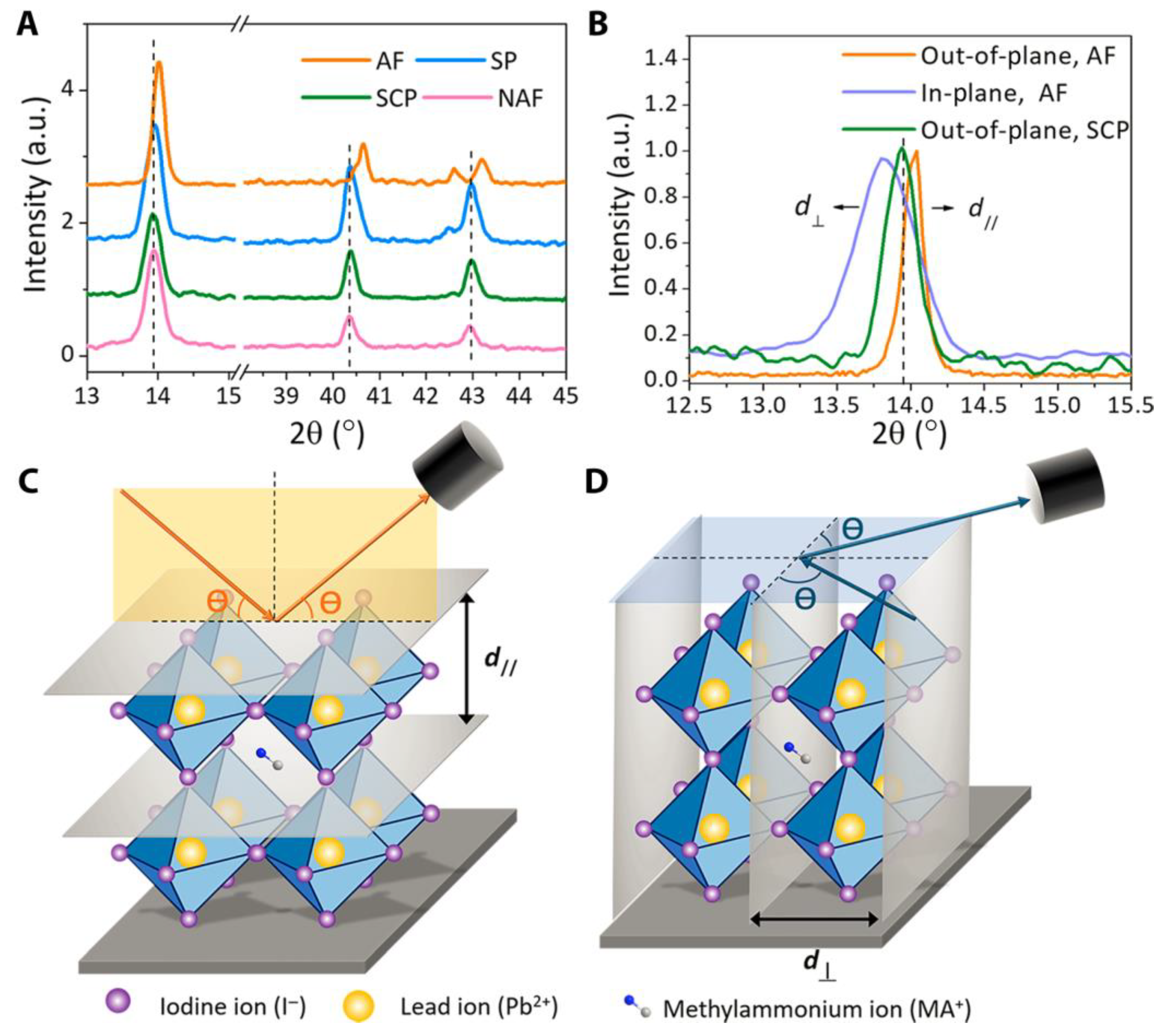
Scheme 3.
Schematic representation of two possible ferroelectric domain walls: domain type 180◦ and 90◦ in a tetragonal structure.
Scheme 3.
Schematic representation of two possible ferroelectric domain walls: domain type 180◦ and 90◦ in a tetragonal structure.
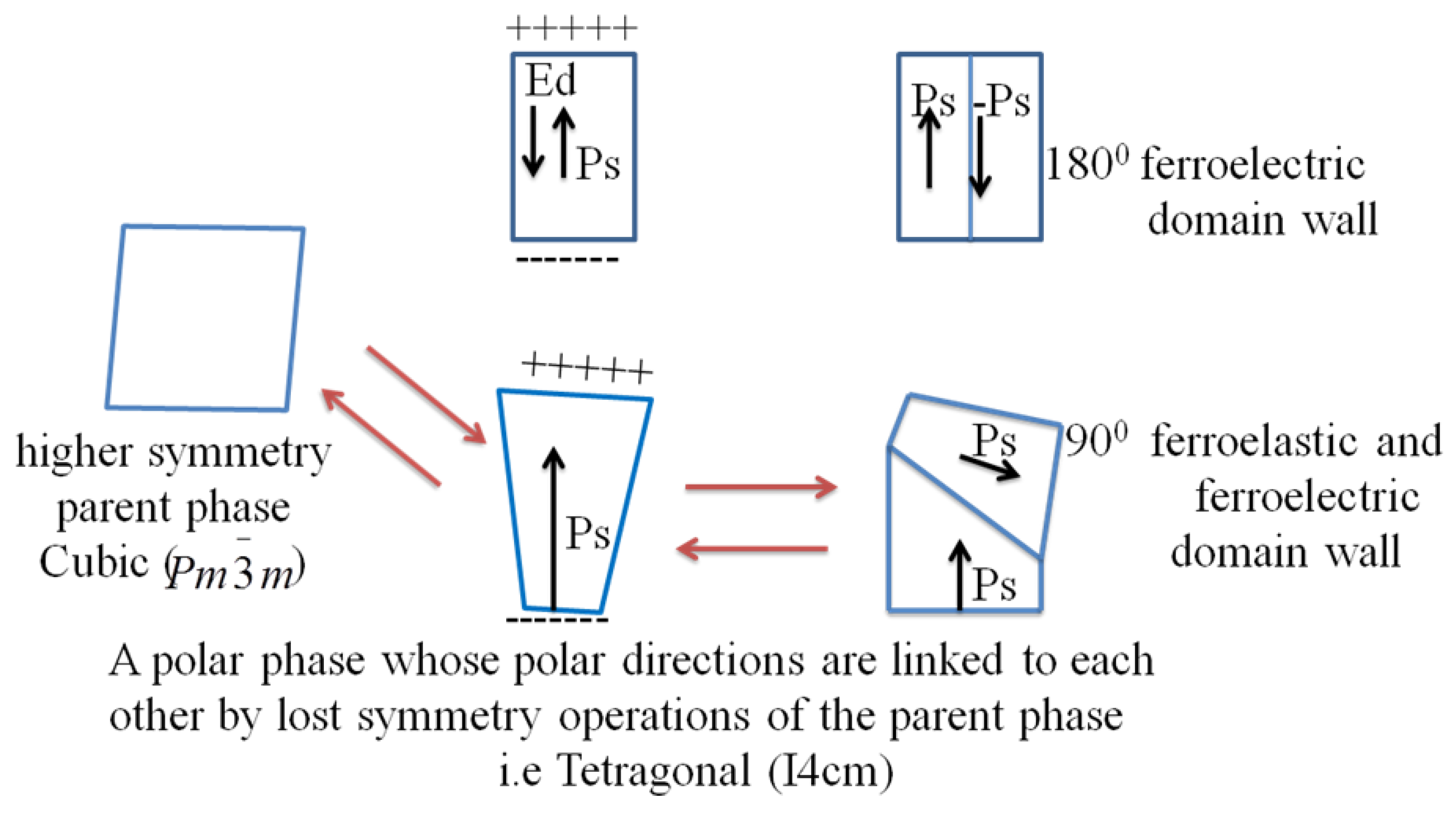
Figure 3.
Polarization hysteresis loop. Reproduced with permission[279] Copyright 2015 Michele Manzo, Doctoral Thesis.
Figure 3.
Polarization hysteresis loop. Reproduced with permission[279] Copyright 2015 Michele Manzo, Doctoral Thesis.
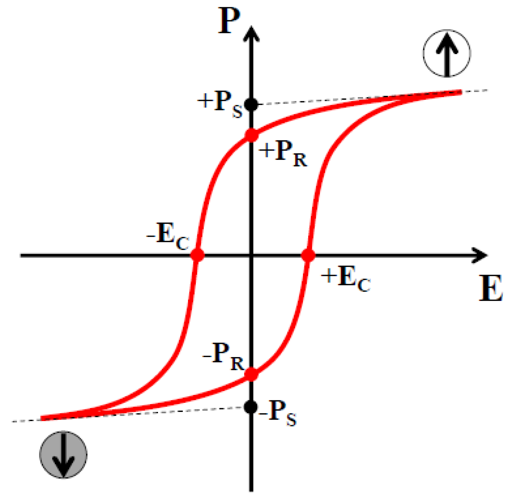
Figure 5.
Electronic structure and piezoelectric response of EDABCO-CuCl4. Reproduced with permission[298] Copy right 2023 Nature publishing group.
Figure 5.
Electronic structure and piezoelectric response of EDABCO-CuCl4. Reproduced with permission[298] Copy right 2023 Nature publishing group.
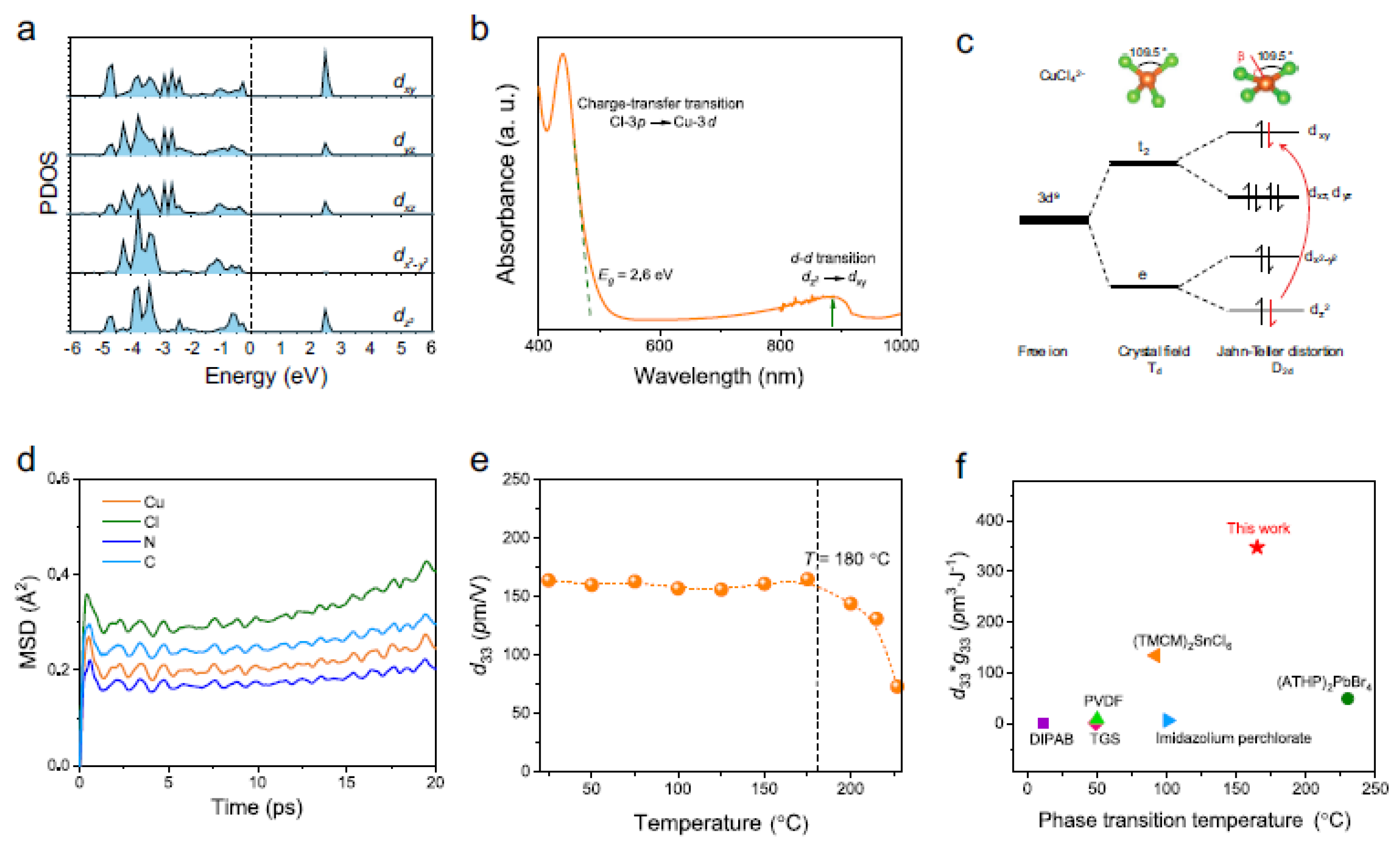
Figure 7.
Piezoelectricity. Reproduced with permission.[345] Copyright 2013 Springer Science+Business Media Dordrecht.
Figure 7.
Piezoelectricity. Reproduced with permission.[345] Copyright 2013 Springer Science+Business Media Dordrecht.
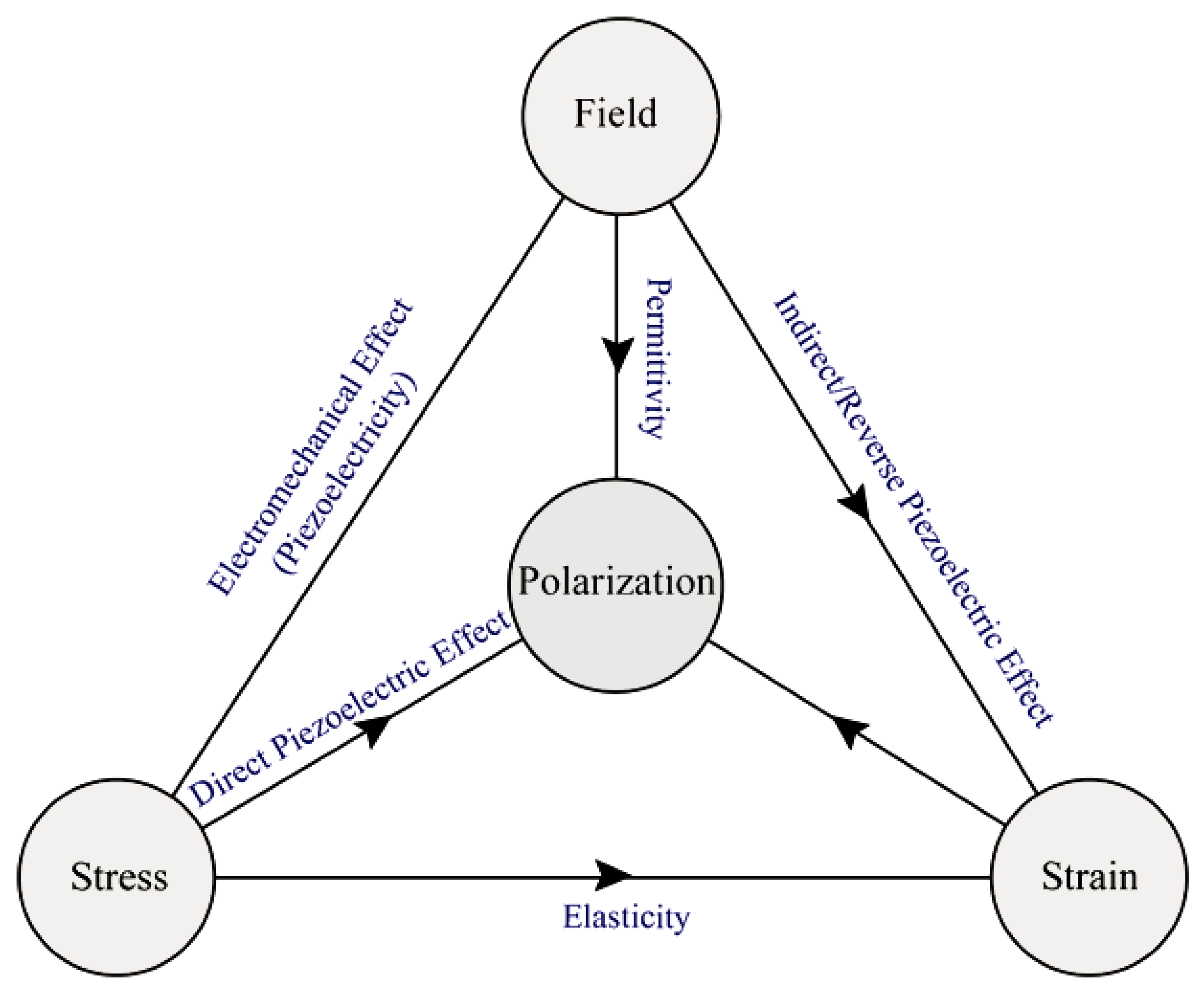
Figure 8.
Schematic representation of simple molecular model for piezoelectric effect: Reproduced with permission.[345] Copyright 2013 Springer Science+Business Media Dordrecht a) An unperturbed molecule with no piezoelectric polarization; b) The perturbed molecule exposed to an external force (Fk); c) polarization effect.
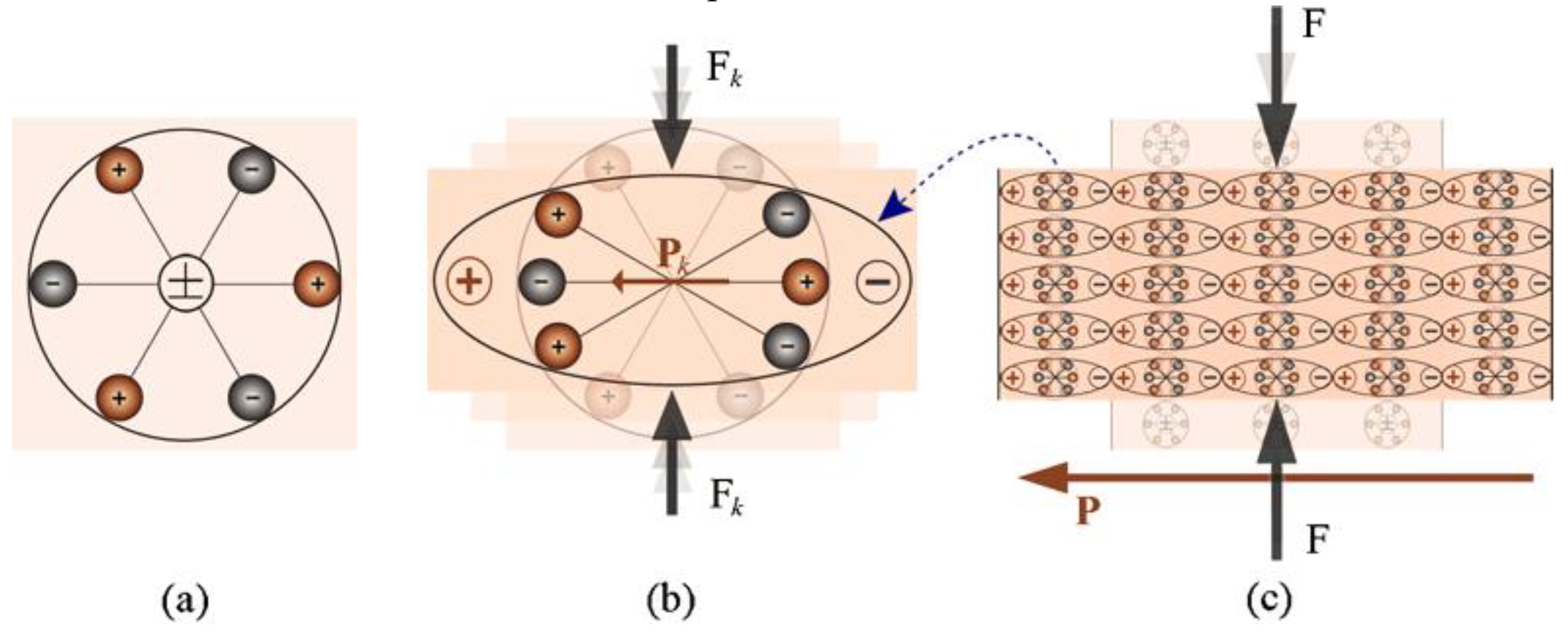
Figure 9.
Relative permittivity and pyroelectric response measurements. Reproduced with permission.[347] Copyright 2011 Macmillan Publishers Limited.
Figure 9.
Relative permittivity and pyroelectric response measurements. Reproduced with permission.[347] Copyright 2011 Macmillan Publishers Limited.
Figure 10.
Schematic demonstration of the structure, mechanisms and Pyroelectric effect induced of self-powered ZPH PDs. Reproduced with permission.[358] Copy right 2015 Macmillan Publishers Limited.
Figure 10.
Schematic demonstration of the structure, mechanisms and Pyroelectric effect induced of self-powered ZPH PDs. Reproduced with permission.[358] Copy right 2015 Macmillan Publishers Limited.
Figure 11.
Process of strain formation. Reproduced with permission[58] Copyright 2017 American Association for the Advancement of Science.
Figure 11.
Process of strain formation. Reproduced with permission[58] Copyright 2017 American Association for the Advancement of Science.
Figure 12.
The presence of Strain study in (FAPbI3)0.85(MAPbBr3)0.15. Reproduced with permission.[360] Copy right 2019, Nature publishing group.
Figure 12.
The presence of Strain study in (FAPbI3)0.85(MAPbBr3)0.15. Reproduced with permission.[360] Copy right 2019, Nature publishing group.
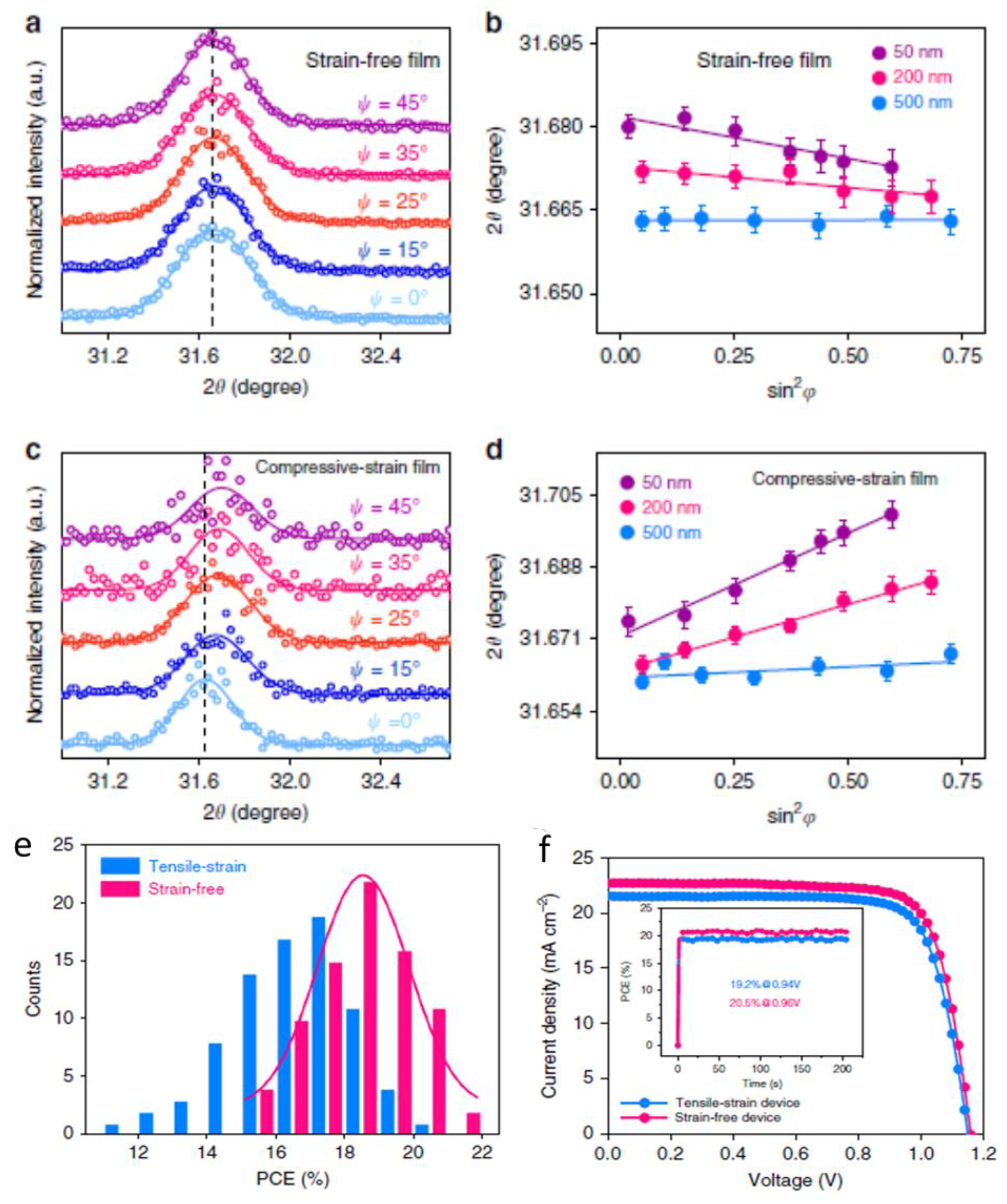
Figure 13.
Photoinduced interaction and configuration of PiFM. Reproduced with permission.[414] Copyright 2015 American Chemical Society a) Representation of the interaction between the photoinduced tip dipole in the focal plane of a tightly focused field and in the target particle. b) Configuration of the PiFM.
Figure 14.
Instrumentation: Reproduced with permission.[444] Copyright 2013, American Chemical Society. (a) Picture of the PTIR technique: (b) high peak to peak deflection (c) getting amplitude of different contact resonance modes.
Figure 14.
Instrumentation: Reproduced with permission.[444] Copyright 2013, American Chemical Society. (a) Picture of the PTIR technique: (b) high peak to peak deflection (c) getting amplitude of different contact resonance modes.
Figure 15.
Dielectric study of the mixed halide-MAPbI3 films: Reproduced with permission[108] Copy right, 2020 American Chemical Society.
Figure 15.
Dielectric study of the mixed halide-MAPbI3 films: Reproduced with permission[108] Copy right, 2020 American Chemical Society.
Figure 16.
Hybrid perovskite piezoelectric nanogenarator structure. Reproduced with permission.[325] Copyright 2016 WILEY-VCH Verlag GmbH & Co. KGaA, Weinheim.
Figure 16.
Hybrid perovskite piezoelectric nanogenarator structure. Reproduced with permission.[325] Copyright 2016 WILEY-VCH Verlag GmbH & Co. KGaA, Weinheim.
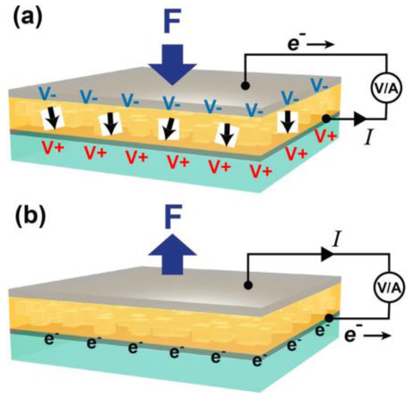
Figure 17.
Various alternative cantilever beams as the structure base of the piezoelectric generator. Reproduced with permission.[472] Copyright 2013 Pomiary Automatyka Robotyka.
Figure 17.
Various alternative cantilever beams as the structure base of the piezoelectric generator. Reproduced with permission.[472] Copyright 2013 Pomiary Automatyka Robotyka.
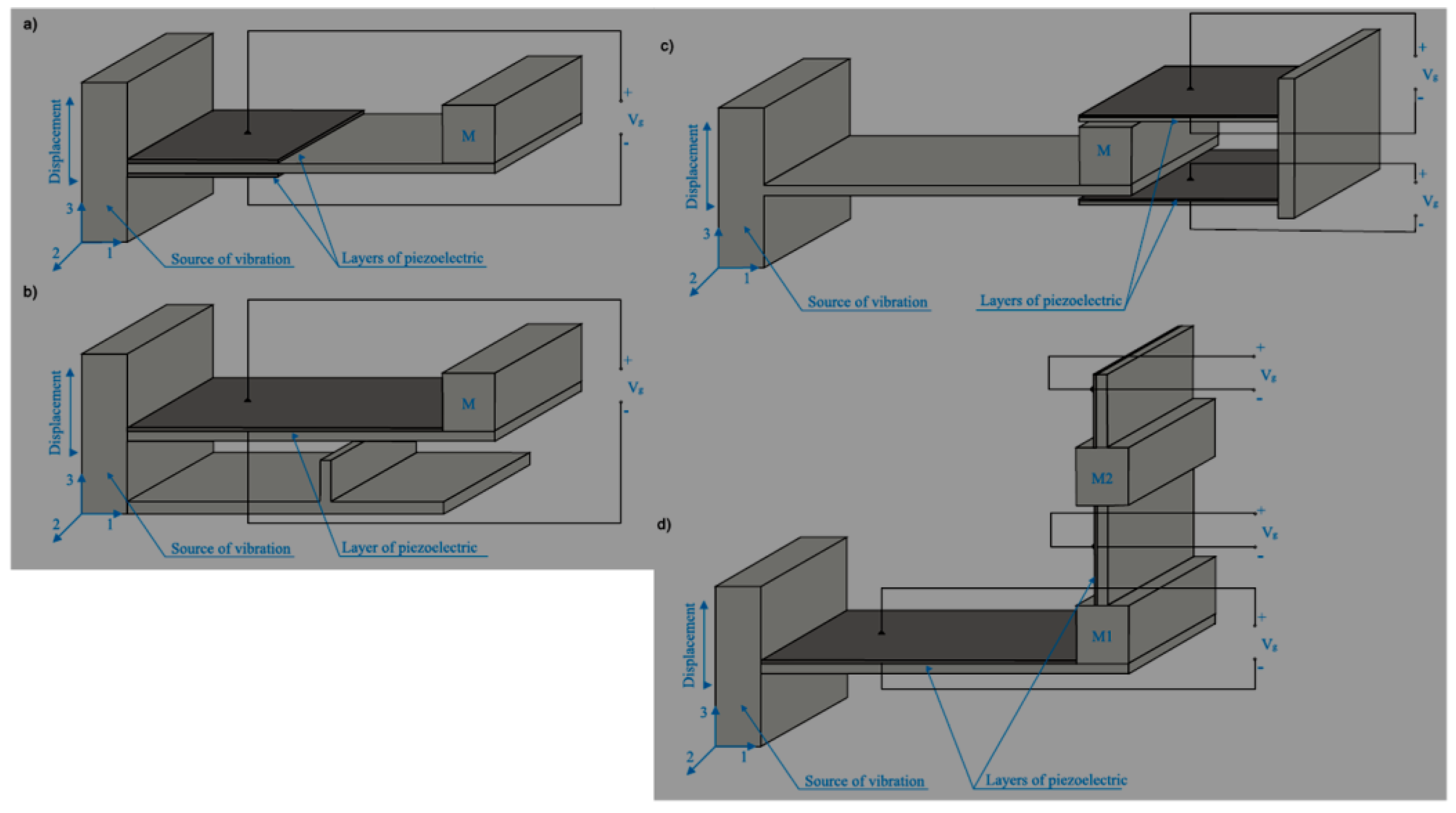
Figure 18.
Cross-sections of the beam in generators. Reproduced with permission. [475] Copyright 2010 from Proceedings of PowerMEMS.
Figure 18.
Cross-sections of the beam in generators. Reproduced with permission. [475] Copyright 2010 from Proceedings of PowerMEMS.
Figure 19.
Important coupling modes for piezoelectric materials. Reproduced with permission.[478] Copyright 2004 Institute of Physics Publishing (Smart Materials and Structures) (a): ‘33’ coupling mode, (b): ‘31’ coupling mode.
Figure 19.
Important coupling modes for piezoelectric materials. Reproduced with permission.[478] Copyright 2004 Institute of Physics Publishing (Smart Materials and Structures) (a): ‘33’ coupling mode, (b): ‘31’ coupling mode.
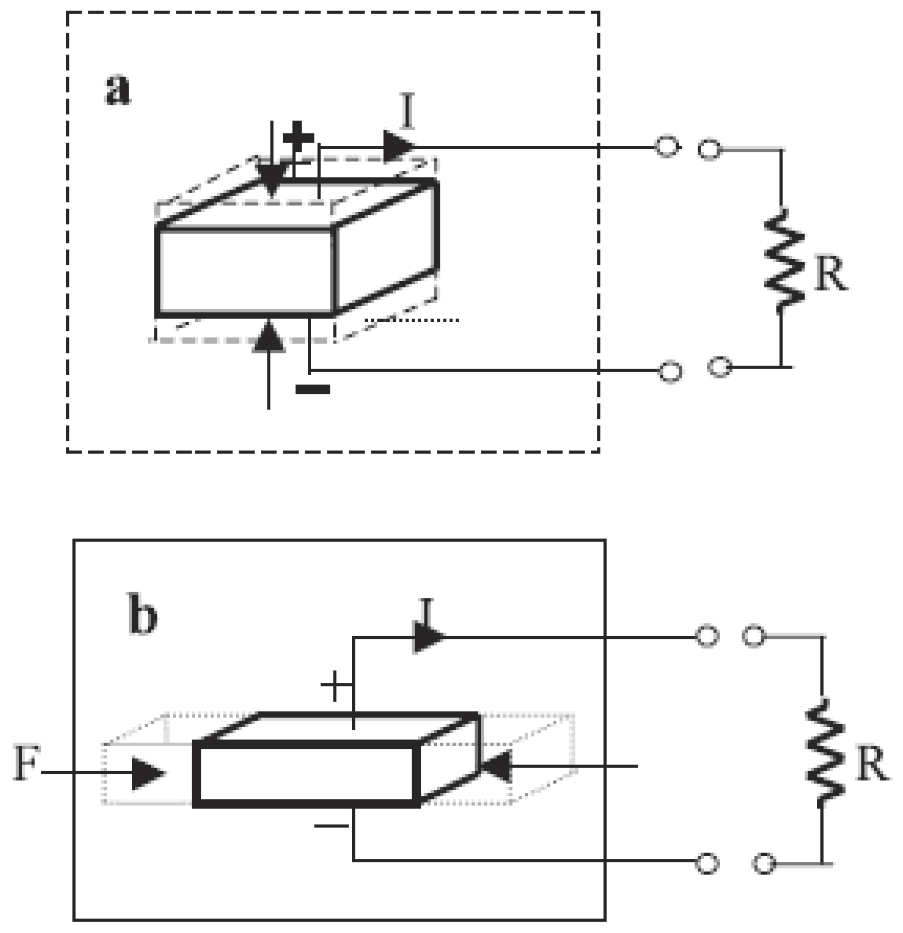
Figure 20.
Damping and Modes of Energy harvesting. Reproduced with permission.[493] Copyright 1991, IOP Publishing. a) Representation of vibration damping. Is it possible to replace PZT ceramic by CH3NH3PbX3 or MPbX3 composite for vibrating damping, where M is metal with +1 cation and X is halides? Frequent models of piezoelectric energy harvesting devices: b) Piezoelectric 33- Model and c) Piezoelectric 31- mode.
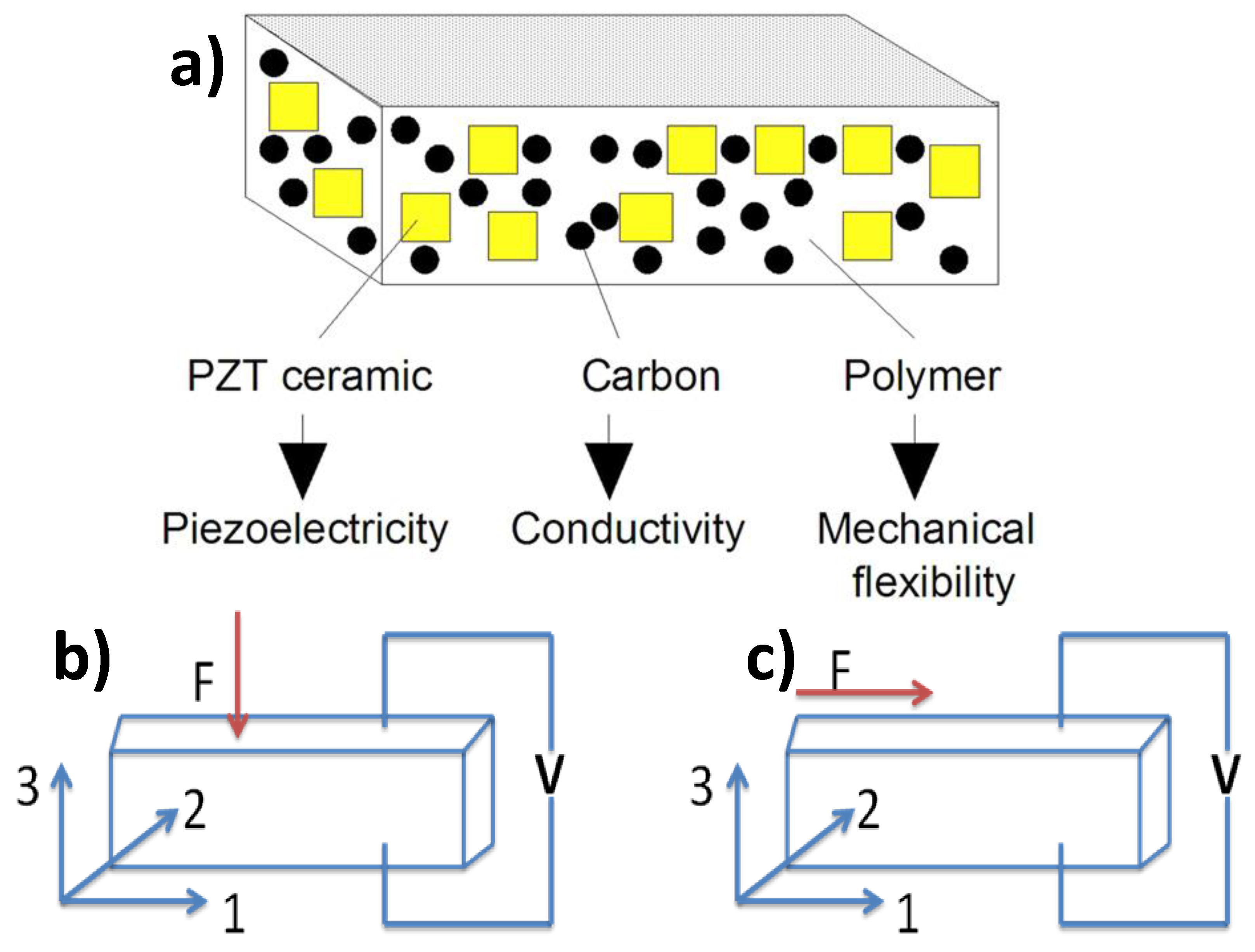
Figure 21.
Working mechanism of self-powered ZPH PDs. Reproduced with permission.[358] Copy right 2015 Macmillan Publishers Limited.
Figure 21.
Working mechanism of self-powered ZPH PDs. Reproduced with permission.[358] Copy right 2015 Macmillan Publishers Limited.
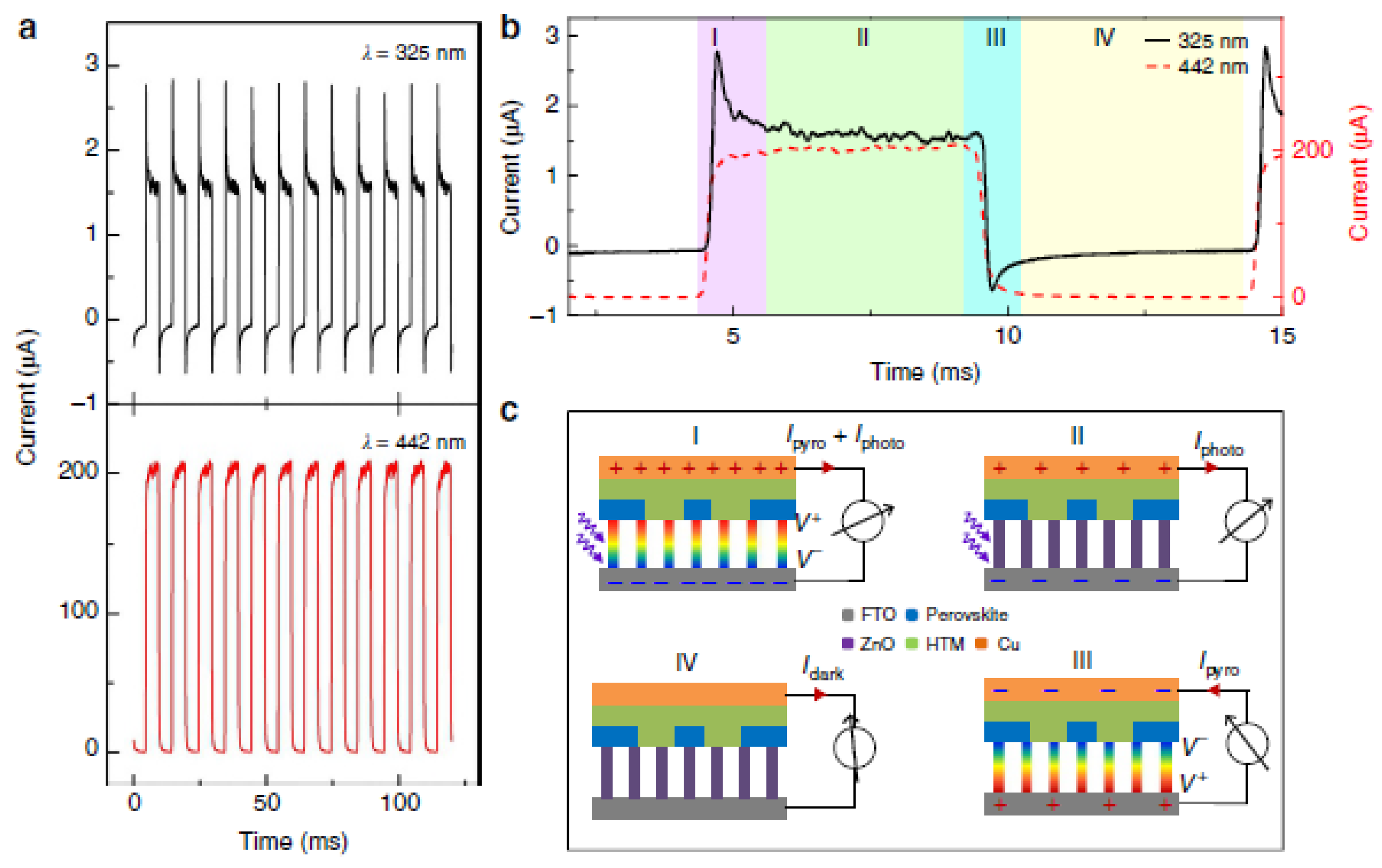
Figure 22.
Photoflexoelectricity: Reproduced with permission[517] Copy right 2020, Nature publishing group. a) polarization of MAPbBr3 up on bending in the dark and light, b) flexoelectric coefficients of various perovskite oxides and halides.
Figure 22.
Photoflexoelectricity: Reproduced with permission[517] Copy right 2020, Nature publishing group. a) polarization of MAPbBr3 up on bending in the dark and light, b) flexoelectric coefficients of various perovskite oxides and halides.
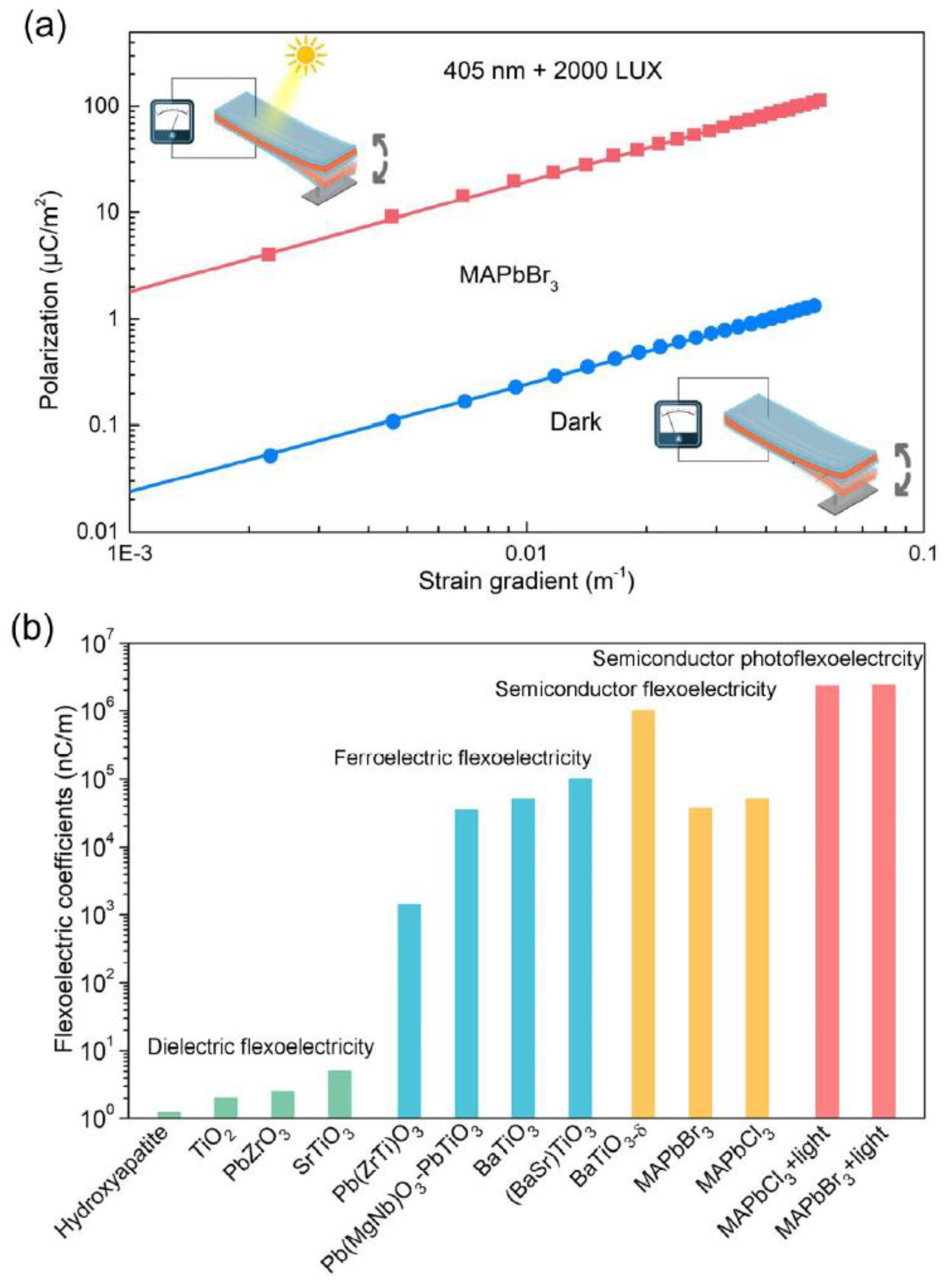
Figure 23.
Biased hysteresis loops which may arise owing to the presence of defects in a ferroelectric crystal.
Figure 23.
Biased hysteresis loops which may arise owing to the presence of defects in a ferroelectric crystal.
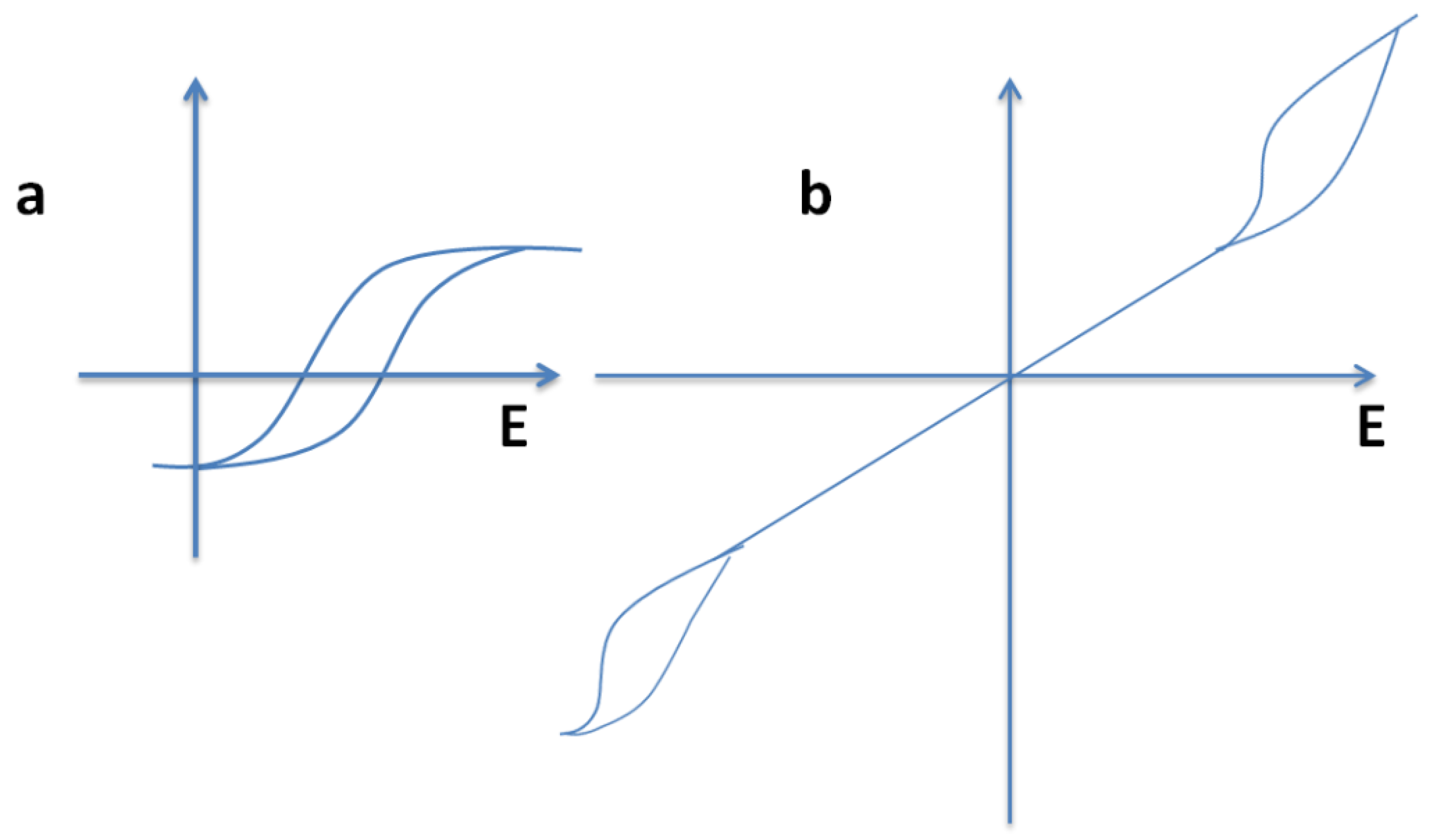

Table 1.
Composition dependent ferroelectric halide perovskite materials.
| Material | Eg/ eV | d33 /pCN−1 |
Ps / μC cm−2 |
TC /K | Young’s modulus/GPa | Symmetry change |
|---|---|---|---|---|---|---|
| (TMFM)x(TMCM)1–xCdCl3[137] | - | 1540 | - | 366.8 | - | - |
| MAPbI3[138,139] | 1.56 | - | 7.2 to~8 but 38 is expected | 330 | E[100] =10.4 | I4cm to Pmm |
| BaTiO3[140] | - | 190 | 26 | 393 | - | - |
| Tetragonal to orthorhombic MAPbBr3[141] | 2.2 | - | ∼0.35 to ∼0.4 | - | - | Pna21 to I4cm |
| CsPbI3[142,143] | 1.73 | - | - | - | 186 | Pnma to Pmn21 |
| MAPbI3-xClx[144] | 1.57 to 1.63 | - | - | - | - | - |
| NH4PbI3[114] | 1.76 | - | 5.4 | - | ||
| (ChPy)4AgBiBr8[145] | - | - | 3.2 | 305 | - | - |
| (MDABCO)RbI3[146] | 14 | 22 | 448 | R3 to P432 | ||
| MPSnBr3[147] | 2.62 | - | 4.5 | 357 | - | Pna21 to Pm¯3m |
| 3-APRbBr3[148] | - | - | - | 440 | Pm¯3m to Ia | |
| MDABCONH4X3 (X=Cl−, Br− and I−)[111,149] | 119, 248 and 178 | - | 14.7, -,- | - | ||
| MHy2PbBr4[145] | - | - | 5.8 | 351 | - | Pmn21 to Pmnm |
| MAPb(I1-xBrx)3[150] | - | - | - | - | - | |
| CH3NH3SnI3[151] | 1.30 | - | - | - | - | - |
| N(CH3)4SnI3[152] | 2.12 | - | 16.13 | - | - | R3m |
| FAPbI3[153] | 1.47 | - | - | E[100] = 11.8 | P3m1↔P63mc | |
| MAPbCl3[154,155,156,157,158] | 2.9 | - | - | - | E[100] =19.8 | - |
| TMIM-PbI3[159] | - | - | 0.67 | 312 | - | C2↔C2/m |
HC(NH2)2+ = FA, trimethylbromomethylammonium=TMIM, MDABCO = N-methyl-N′-diazabicyclo[2.2.2]octonium, ChPy = chloropropylammonium, 3-AP = 3-ammoniopyrrolidinium, TMFM = trimethylfluoromethyl ammonium, TMCM = trimethylchloromethyl ammonium.
Table 2.
Values of the electric power for halide peroveskite selected energy harvesters.
| Energy harvesting materials | Output voltage/V | Output current density/ | Current | specific capacity | d33 | Reference |
|---|---|---|---|---|---|---|
| 4Cl-MAPbI3 PENG | 5.9 | ∼0.61 μA/cm2 | [108] | |||
| CsPbCl3 | 257 | 3.04 Wm-2 | 27.87 μA | [456] | ||
| FASnI3:PVDF | 23 | 35.05 mWcm–2 | 73 pm/V | [103] | ||
| FASnBr3 | 94.594.5 Vp-p | 18.95 μW/cm2 | 19.1 μAp-p | 5050 pm/V | [105] | |
| MA2SnCl6 | 7.33μW cm-2 | 589.98 mAh g-1. | [104] | |||
| Cs2NaBiCl6 | Stable 300 mAh g–1 | [457] | ||||
| TMCM2SnCl6 | 81 | 0.6 kV/cm | 2 μA | 137 pC/N | [257] | |
| CH3NH3PbBr3 | 175.5 mAh g–1 | [458] | ||||
| CH3NH3PbI3 | 2.7 | 140 nAcm_2 | 43.6 mAh g–1 | 5.12 pm/V | [458] | |
| CH3NH3PbBr3:3Li+ | 200 mAhg−1 | [459] | ||||
| CsPb2Br5 | 200 | 45 mW | 2.8 | 72 pmV_1 | [460] | |
| Poled CH3NH3PbI3 | 2.7 | 140 nAcm_2 | [454] | |||
| Li4Ti5O12 | 175.5 mAhg−1 | [461] | ||||
| BaTiO3 | 6.5 | 70 nAcm-2 | [460] | |||
| EDABCO-CuCl4@PVDF | 63 | 43 µW/cm2 | 2.1 μA/cm2 | 165 pm/V | [298] |
EDABCO = N-ethyl-1,4-diazoniabicyclo[2.2.2]octonium), PVDF (polyvinylidene fluoride),.
Table 3.
Perovskite-phase metal oxides and halides: Properties and Applications[323,325,455,462,466,467].
| Materials | Properties | Applications |
|---|---|---|
| (Ba,Sr)TiO3 | pyroelectric | pyrodetector |
| BaTiO3 | dielectric | capacitor, sensor |
| PbTiO3 | piezoelectric pyroelectric | acoustic transducer pyrodetector, |
| Pb(Zr,Ti)O3 |
pyroelectric piezoelectric dielectric electro-optic |
pyrodetector surface acoustic wave device, substrate nonvolatile memory, waveguide device |
| (Pb,La)(Zr,Ti)O3 | electro-optic pyroelectric | waveguide device, optical memory display pyrodetector |
| (LiNbO3/Ti) | electro-optic |
waveguide device, second harmonic generation, optical modulator |
| LiNbO3 | piezoelectric | pyrodetector, surface acoustic wave device |
| K(Ta,Nb)O3 |
electro-optic pyroelectric | waveguide device, frequency doubler pyrodetector |
| Pb(Mg1/3Nb2/3)O3 | dielectric | memory, capacitor |
| FAPbBr3 | Piezoelectric pyroelectric electro-optica |
Piezoelectric nanogenerator Acoustic transducera, pyrodetectora Waveguide devicea, second harmonic generation?, optical modulators? |
| MAPbI3 | Piezoelectric, Pyroelectric, Electro-opticsa |
Piezoelectric energy harvesting devices, Acoustic transducera, pyrodetectora Waveguide devicea, second harmonic generationa, optical modulatorsa |
| CsPbX3 | Piezoelectrica Pyroelectrica Electro-opticsa |
Piezoelectric energy harvesting devicesa, Acoustic transducera, pyrodetectora Waveguide devicea, second harmonic generationa, optical modulatorsa |
| Structure of piezoelectric generator |
Piezoelectric material |
Dimension of piezoelectric material [mm] |
Dimension of generator [mm] |
Frequency of source vibration [Hz] |
Generated Power [mW] |
|---|---|---|---|---|---|
| Cantilever beam | PZT | 4 × patches: 25,4×50,8×0,254 |
14,3×50,8×1,27 | 29,5 | 1.4 |
| Cantilever beam | MFC | 2 × patches: 85×28×0,3 |
114,3×50,8×1,27 | 29,7 | 1.7 |
| Connected four cantilever beams |
PZT | 4 × patches: 30×10×0,5 |
200×200×0,2 | 35,5 | 8.0 |
| M-shaped beam | PZT | 2 × patches: 25×25,4 |
220×25,4×0,254 | 14.5 | 2.6 |
| Cantilever | FAPbBr3 | - | 1×3 | - | 32.3 x 10⁻³ |
Table 5.
Reported performance of nanogenerators made of hybrid composite piezoelectric materials.[325,487,488,489,490,491].
| Nanogenerator | Output voltage [V] |
Output current | Efficiency |
|---|---|---|---|
| NaNbO3/PDMS | 3.20 | 16 nA cm−2 | - |
| LiNbO3/PDMS | 0.46 | 9.11 nA | - |
| BaTiO3/PDMS | 5.50 | 350 nA | - |
| ZnSnO3/PDMS | 9.70 | 0.9 μA cm−2 | - |
| PMN-PT/PDMS | 7.80 | 2.29 μA | - |
| FAPbBr3/PDMS | 8.50 | 3.4 μA cm−2 | 0.44% |
| MAPbX3/PDMS | ? | ? | ? |
| CsPbX3/PDMS | ? | ? | ? |
Note that the symbol ‘?’ indicates research question which need further investigation in the future applications of halide perovskites.
Table 6.
Halide perovskite based nanosensing .
| Nano-sensing devices | Sensitivity %/kPa−1 | LOD | Ref. |
|---|---|---|---|
| CsPbBr1.5I1.5 /TiO2 | 0.012 μM | [525] | |
| NIPs@ CsPbBr3 QDs | 1.45 ng/mL. | [526] | |
| HC(NH2)2SnI3/SnO2/Pt-NPs nano-composite | 65 ppb | [527] | |
| MAPbI3_x(SCN)x | 3 | [528] | |
| ZnO nano-sheets/MAPbI3 | 0.57 | 0.5 | [529] |
| CH3NH3PbI3−xClx based ozone sensor | 9.69 | [530] | |
| (RNH3)2 PbI4 | 1.3 | [531] | |
| CsPbX3 quantum dot with Oleic acid ligand | 0.1 nM | [532] | |
| CsPbX3 (Br/I) Quantum dots/picric acid | 0.8 nM | [533] | |
| CsPbBr3 QDs/Cu2+ and Yb3+ ions | 2 × 10⁻⁵ m | [534] | |
| CsPb(Br/Cl)3 nanocrystals | 5 ppm | [535] | |
| CsPbBr3 QDs film | 8.85 ppm | [536] | |
| Cs3Bi2Br9:Eu3+ PeQDs | 10 nM | [537] | |
| CH3NH3PbI3 based NH3 gas sensor | 55 | 10 ppb | [538] |
| CH3NH3PbI3−x(SCN)x for NO2 detection | 5.3 × 10⁻¹ ppm−1 | 200 ppb | [539] |
| MAPbBr3 room-temperature NO2 sensors | 0.1 ppm | [540] | |
| (MA)2Pb(SCN)2I2 for O3 detection | 5 ppb | [541] | |
| CsPbBr3 nanocubes | 54% | 187 ppb | [542] |
| Dual ligands capped CH3NH3PbBr3 QDs | 3.2 μM | [543] | |
| MAPbI3 thin films on SiO2 | 70 ppm | [544] | |
| CH3NH3PbI3−xClx hydrogen sensing | 10 ppm | [545] | |
| CsPbBr3 QDs for H2S detection | 0.18 μM | [546] | |
| Porous CsPbBr3 network | 1 ppm | [547] | |
| MAPbI3 pellet sensor | 200 % | [548] | |
| Ethylenediamine lead iodide chloride (EDPIC) perovskite thin film |
65% | [549] | |
| Paper coated with MAPbI3 | 55% | [550] | |
| (APTES)-capped CsPbBr3 QDs | 18.8 ng/mL | [551] | |
| AuN@(CsPbBr3NCs@BaSO4)@ melamine | 0.42 nmol/L | [552] |
Disclaimer/Publisher’s Note: The statements, opinions and data contained in all publications are solely those of the individual author(s) and contributor(s) and not of MDPI and/or the editor(s). MDPI and/or the editor(s) disclaim responsibility for any injury to people or property resulting from any ideas, methods, instructions or products referred to in the content. |
© 2024 by the authors. Licensee MDPI, Basel, Switzerland. This article is an open access article distributed under the terms and conditions of the Creative Commons Attribution (CC BY) license (http://creativecommons.org/licenses/by/4.0/).
Copyright: This open access article is published under a Creative Commons CC BY 4.0 license, which permit the free download, distribution, and reuse, provided that the author and preprint are cited in any reuse.


