
Submitted:
12 September 2024
Posted:
14 September 2024
You are already at the latest version
Abstract
Loop-Mediated Isothermal Amplification (LAMP) is a widely used technique for nucleic acid amplification due to its high specificity, sensitivity, and rapid results. Advances in microfluidic lab-on-chip (LOC) technology have enabled the integration of LAMP into miniaturized devices, known as μ-LAMP, which require precise thermal control for optimal DNA amplification. This paper introduces a novel thermal bed design using PCB copper traces and FR−4 dielectric materials, providing a reliable, modular, and repairable heating platform. We present the design, fabrication, and control mechanisms of the thermal bed, demonstrating its ability to maintain accurate temperatures essential for μ-LAMP applications. The thermal bed’s performance is validated through finite element method (FEM) simulations, confirming its effectiveness in diverse applications such as disease diagnostics, biological safety, and forensic analysis.
Keywords:
LAMP
; DNA amplification
; microfluidics
; thermal control
; optoelectronic sensors
1. Introduction
Advances in molecular diagnostics have underscored the need for rapid and accurate nucleic acid amplification techniques. Loop-Mediated Isothermal Amplification (LAMP) is a powerful method known for its high specificity and sensitivity in DNA amplification under isothermal conditions. The integration of LAMP into microfluidic lab-on-chip (LOC) systems, termed -LAMP, allows for miniaturization and automation, greatly enhancing the efficiency of molecular diagnostics. However, the success of -LAMP is highly dependent on precise thermal control systems that can maintain stable temperatures to ensure optimal DNA amplification.
This paper presents a novel thermal bed design using printed circuit board (PCB) copper traces with dielectric materials, offering precise and stable temperature control for DNA amplification. The thermal bed integrates optoelectronic sensors to monitor temperature and colorimetric changes, which are crucial for assessing amplification progress. This design provides a modular and repairable platform suitable for disease diagnosis, biological safety monitoring, and forensic analysis [1,2,3,4,5].
The -LAMP method, widely utilized for nucleic acid amplification, facilitates DNA synthesis in approximately 20 minutes with high specificity, sensitivity, and minimal initial fluid requirements. Lab-on-chip (LOC) technologies have potential for numerous applications, including disease diagnosis, biological safety, food analysis, and pathogen detection. The successful implementation of this technology could revolutionize sample processing in forensics, significantly reducing the time required to handle backlogged cases, such as rape kits. The integration of LAMP with microfluidic chip technology has led to the development of -LAMP [6,7,8,9,10,11,12,13,14,15].
There is growing interest in implementing biological processes for chemical evaluation and analysis across various disciplines. Biology, chemistry, and medicine increasingly demand technologies that can perform laboratory procedures quickly and with minimal manual intervention. These advances often employ autonomous self-regulating devices to reduce human error and improve precision [16,17,18,19,20,21,22].
Optimizing parameters to improve DNA amplification reliability involves selecting appropriate thermoelectric components, designing the thermal fluid chamber, and integrating optical sensors with instrumentation and control systems. These elements are critical in monitoring and characterizing DNA amplification processes that involve feedback control mechanisms. Efficient temperature management is vital for the functionality of the -LAMP process, underscoring the importance of robust thermal control systems [23,24,25,26,27,28,29,30,31,32,33].
2. Methodology
The analysis focuses on the temperature increase caused by Joule’s law, created by current flow in a closed circuit. Precise control of the electric current determines the temperature increase, guiding the selection of physical parameters and materials for the thermal bed.
The device includes all design phases, from introducing the fluid mixture to completing the DNA amplification process. Two optoelectronic sensors play a key role in process control: one for temperature measurement and another for color detection, monitoring the amplification progress. The temperature is sampled at a single reference point to correlate with the sample’s temperature, verified through repeated simulations with varying system parameters. Detecting the precise completion of the process, especially with the miniaturized motility sensor, presents a challenge. An optical sensor detects color changes due to turbidity shifts in the sample, calibrated to ensure accurate control of the -LAMP process with miniaturized electro-optical sensors and precise temperature measurements. Introducing a small volume of fluid samples for DNA testing poses a technological challenge not covered in this work.
This paper presents a model for the electric current distribution leading to controlled temperature increases, crucial for a DNA amplification device operating at 62 °C. We introduce a novel thermal bed design that utilizes advances in semiconductor technology, specifying the thermoelectric parameters of copper tracing for effective implementation. Using the finite element method (FEM), we simulate the copper trace as a thermal bed for the sample chamber and evaluate its temperature performance under various electrical current levels.
2.1. Thermal Bed Design
Figure 1 shows the block diagram presenting the architecture of the DNA amplification device. The hardware includes the copper trace heated with current whose magnitude is defined by the pulse width modulation (PWM) method. The thermoelectric system generates the necessary heat to elevate and maintain the temperature of the sample chamber contents. Its control subsystem ensures that the temperature remains within set limits, utilizing a copper trace integrated into a printed circuit board (PCB). A temperature sensor is strategically placed inside the fluid chamber to monitor conditions. The microprocessor adjusts the current through pulse width modulation (PWM) to regulate the temperature as needed. A modified optical turbidity sensor functions as an optical color sensor to detect the completion of DNA amplification. The microprocessor interprets the output of this sensor to identify when the color change indicates that DNA amplification is complete.
In our system design, hardware elements are represented with orange boxes, communication protocols with blue lines and boxes, and sensors, detectors, PC interface, and the power system for the PCB trace are represented with green boxes. A dsPIC® DSC microprocessor manages the device’s control, while the power supply on the upper right manages the energy distribution to the thermoelectric heating stage via PWM. An RGB LED is digitally controlled by the microprocessor for process visualization. Data transmission is illustrated in the lower left-central part, demonstrating compatibility with Bluetooth, ZigBee, and any wireless or wired communication support device.
We developed a mathematical model to evaluate the current distribution across the PCB traces, optimizing the physical and mechanical parameters and the geometric configuration for implementation on the chip. Thermoelectric simulations using the finite element method (FEM) were conducted to confirm that the proposed increase in temperature per current is appropriate. The PCB design software also implemented the copper trace configuration to simulate and ensure a homogeneous thermal distribution throughout the fluid volume.
After simulations, the selection of electronic components for the test PCB card was performed to validate the design. The thermal bed uses a specific current tailored to the PWM to match the electrical specifications of the components, including transistors and controllers, ensuring the functionality and longevity of the device. The DNA amplification process, accelerated using the procedure, operates at a stable temperature of . The methodologies described can also model and optimize other methods that require different temperatures, such as those starting around .
Providing a controlled temperature environment is crucial for a range of processes and applications in fields such as biology, medicine, chemistry, and forensics [7,28]. The primary objective is to replicate DNA or develop new methodologies for analyzing biological events. Various heating mechanisms have been implemented to control the temperature in these systems. Recent advances have focused on the thermal management of -LAMP devices, including silicon arrays for temperature control in PCR amplification [24,25], micro-coils for temperature regulation in Lab-On-Chip platforms, and thermistors and thin-film manufacturing for PCR applications [27,28,34,35].
This study follows the IPC Industrial and Thermoelectric Standards Model (Association of Connecting Electronic Industries [36]). Following the selection of the physical characteristics of the copper trace and the power supply, the simulations analyzed the thermal resistance of the PCB, establishing the relationship between the increase in temperature and the required electrical current. The current and its control unit automatically provide the necessary temperature increase without manual intervention.
To optimize DNA amplification, thermal specifications must be met. The control mechanisms raise the temperature to the desired operating point and maintain it for the duration required for DNA amplification. Subsequently, the mechanical parameters of the PCB trace are defined.
Figure 2 illustrates the characteristics of the PCB used in the thermal bed design. Figure 2(a) shows the cross-section of an analyzed PCB segment. The thickness of copper remains consistent throughout the PCB layer, according to the chosen copper foil: 1 Oz ft −2 in this case. The width of the copper trace is defined in the design program parameters and measured in mils (0.001 in = 1 mil = 0.025 mm). Modifying the width of the trace adjusts its impedance, allowing control over the current capacity for that segment of the copper trace. The target temperature increase and electrical current must be considered to propose an optimal trace width.
The design and manufacturing standard for PCBs, , proposes an approximation of the increase in temperature of a trace as a function of the electric current flowing through it. This expression limits the physical geometry of the width of the trace relative to the amount of current given by
Here, I is the electrical current in amperes [A], A is the transverse cross-sectional area in , is the temperature increase in [K], and is a constant trace layer of copper such that: = , = . Here, is used for the external layer of the PCB and for its internal layer, known as stripline and microstrip, respectively. This approach works well for panel PCBs with a dielectric thickness of of material and copper conductors with a width of or greater.
Once we have selected the power supply, we can deduce other system parameters from it. Specifically, a copper trace of 10-mil width and a thickness of 1 Oz (a standard PCB specification, equal to ) of copper is considered. Then, the current may be limited to less than 1 A. According to the first law of thermodynamics, the total energy of a closed system is conserved. The only way the power of a system changes is when it crosses the boundaries of the system. This law further determines the way energy crosses system boundaries[37]. The following expression is valid for a closed system:
Here is the total change in power stored in the system in [W]; is the net heat transferred to the system per unit time, also in [W]; and is the net amount of work generated by the system per unit time. The derivative of the first law of thermodynamics may also be applied to a controlled volume or even an open system. This analysis is important for determining the unknown temperature, as in our trace segment. Using it, we choose the current necessary for the requisite temperature increase, considering that no external (mechanical) power sources or sinks exist that might provoke a temperature change. The parameter obtained through this analysis is the temperature change rate as a function of current. The first law of thermodynamics and its derivative with time apply at any instant; therefore, the following expression is valid.
Here, in [W] is the rate of increase of energy within a volume in [W], is the rate of input energy transfer into the volume in [W], is the rate of energy transfer out of a volume, and is the rate of energy generation, likewise in [W]. All of this takes place according to the geometry and materials of the components. Using Eq. 3, we determine the current necessary to increase the temperature, considering that no external mechanical power sources could generate a temperature change. Equation 3 may be interpreted to mean that the rate of increase of thermal or mechanical energy stored in a volume must be equal to the rate at which thermal and mechanical energy enter the volume minus the rate at which thermal and mechanical energy leave the volume, plus the rate at which all energy (thermal and other) is generated within the volume.
Figure 3(a) illustrates how the energy of the system changes with time for a short copper segment, representing a defined volume, and how it is interconnected. The electric current I controls the amount of thermal energy generated per unit of time inside the volume using the resistive heating mechanism. Assuming that no energy flows into the short segment of the copper trace, we obtain the following expression from Equation 3:
The resistive losses produce the rate of energy dissipation, then
Here, I is the electrical current in amperes [A], is the electrical resistance of the copper trace per unit of length [], and L is the length of the trace segment in [mm]. The temperature increment of the copper trace is uniform within the volume because a concise segment is considered. This temperature increase may be found as a function of the energy increment rate within the copper trace volume.
Where q is the rate of energy increment per unit of volume. Substituting the volume parameters for the geometry in our design, we have
Here, w and are the width and thickness of the copper trace, in [m] respectively. In this system, thermal energy includes convection and radiative transfers away from the surface of the copper trace. The next equation represents the convection and radiative losses, considering only the surfaces exposed to air and the background temperature[37].
Where h is the heat transfer coefficient for convection in []; is the Stefan-Boltzmann constant, X []; is the emissivity of copper that is between and , without units; and and are the temperatures of the outer layer of the copper trace volume and of the background in [K], respectively. The rate of energy increase within a volume is given by:
Here, is the mass density in [], c is the specific heat capacity in [], and V is the volume of the copper trace, []. In the case of the copper trace, the mass density is 8933 , and the specific heat capacity is 385 []. Substituting Equations 4 through 8 into Equation 9, we solve it for the copper trace’s temperature increase as a current function.
we summarize the quantities for the sake of completeness. T is the temperature increase in [K]; t is the time in [s]; I is the current in amperes, [A]; is the electrical resistance of the copper trace per unit length []; h is the convection heat transfer coefficient in [W K−1]; w is the width of the copper trace in [m]; is the thickness of the copper trace in [m]; L is the total length of the trace in [m]; and are the temperature of the outer layer of the copper volume and the environment, in [K], respectively; is the emissivity of the copper trace, between 0.03 and 0.04; is the Stefan-Boltzmann constant, with the value of 5.67 x 10⁻⁸ W K−4; is the mass density of the copper trace, 8,933 ; c is the specific heat capacity of the trace, 385[]; and the star (*) denotes a product.
Equation 5 may be evaluated numerically. Our system is ten mils wide and 1 Oz ft-2 thick copper trace (as proposed in the design). We obtain the following numerical estimate for the increase in temperature as a current function for the proposed copper tracing using a numerical evaluation presented graphically in Figure 3 (b). We see that any final temperature in the range between room temperature (25 °C) to above 100 °C can be reached with a current of less than 0.5 A through the trace. Thus, many processes may be achieved with the technique described here.
We note that a current smaller than 1 A is required to raise the temperature to the process temperature of 62 °C. To increase the system responsivity, the possibility of working with 1 to 2 W power supplies was also explored. Employing a power supply any larger than 1 W may damage the device itself or its constituent electronic components: the temperature increase may exceed their recommended operating conditions. When using a power source with power significantly smaller than 1 W, the system may take too long to reach, or it may never reach, the temperature required for the amplification process.
2.2. Finite Element Method (FEM) Simulations
A section of the copper trace has been drawn in the ANSYS™ program. This simulation program works in the theory of finite elements for structures. Its dynamic mesh is presented in Figure 4(a). The simulation was performed for an electric current input through a cooper trace to determine the current density distribution and the resulting temperature evolution through space and time. First, the current density inside the trace volume is calculated. The current density is a vector quantity whose magnitude is the electric current per unit area to the current flow’s direction. Figure 4(b) The vector current density as a function of the location on the trace. The current density is related to the electric current as follows:
Again, I is the current in amperes, [A]; j is the current density in [A] and S is the surface area in [m2]. In our simulations, copper was considered the preferred material for selecting the trace. This material is also commonly used in the manufacturing of PCBs.
Figure 5 shows twoPCB trace schemes using the finite element method. Figure 5(a) shows the trace with the initial parameters applicable to the system under design. The preliminary current of 500 mA is proposed for an initial temperature of 25 °C. In addition, an electrical reference potential and a fixed reference point for anchoring the motion are considered, shown in the lower right corner. Figure 5(b) shows the distribution of the electric current density vectors throughout the system. It is observed that the magnitude of the current density is greatest when the trace changes direction by 90 degrees. Arrows represent the distribution of the electric current density vectors, their direction, and magnitude.
After calculating the electric current density vectors and using knowledge of the intrinsic parameters of the implemented trace material, it is finally possible to determine the temperature increase in the copper trace as a function of time using the finite element method[38,39,40].
The calculated temperature distributions on the copper trace are shown for two specific times in Figure 6(a) and 6(b). 10 and 11. We can appreciate how the trace starts at a reference temperature of 25 °C in Figure 6 (a). The first half of the trace has already started to be heated at time t = 0.5 s, while the end segment remains at room temperature. After a specific, relatively short time at t = 2.5 s, the trace reaches the target temperature at least for the first half of the trace length, which in this case is 62 °C.
The simulations of the thermoelectric stage of the device are an iterative process, leading to ever-better design solutions compatible with the device’s requirements. With the final design, we are confident that the physical characteristics and thermal response of the unit are compatible with the device performance requirements. During the final, optimized design and simulation iteration we have determined that the trace configuration of 10 mil (0.254 mm) width and 1 Oz ft-2 (34.79 m) height is the optimal one for our prototype development.
2.3. Optoelectronic Sensor Integration
The geometric information of the parameters obtained with the thermal simulations is the data used in a PCB design program. The preliminary design resulting from the upper and lower layers of the thermal bed is shown in Figure 7(a) and 7(b). The thermal stage of the PCB has an effective area of 39.7 X 28.45 . The thermal traces satisfy the design rule of 10 mils (0.254 mm) wide and 10 mils (0.254 mm) of spacing between the traces.
The central hole in the thermal bed is designed to accommodate an external light source if necessary. The four holes near the corners of the card guide the positioning, alignment, and assembly of the fluid chamber, which is constructed from multiple layers of acrylic sheeting placed on top of the card. The green pads on the right side are for attaching a connector. If a jumper cable shorts the connector, the current flows only through the top part. If the connector is open, the current flows through both parts, allowing us to adjust the system’s rate of temperature increase by changing the connector’s state.
Technological advances in processors and reconfigurable systems enable the implementation of control algorithms that stabilize the system temperature. Classic and modified Proportional-Integral-Derivative (PID) temperature control systems are used due to their reliability and adaptability in maintaining a stable reference temperature state [41,42,43]. A PID controller was incorporated to control the system temperature. The PID control is a feedback control system in which the variables corresponding to the stages are proposed as proportional, integral, and derivative, as necessary for this experiment. This control system was programmed through the configuration of registers and libraries of the dsPIC microprocessor. Sensor readings are processed and converted to appropriate values for microprocessor input. The control system’s output is scaled, providing a multiplier factor for the register that controls the PWM duty cycle. This control system is active from the start of the process until DNA amplification is complete, at which point the output commands deactivate. Figure 8 illustrates the block diagram of the second-order control system implemented, including the closed-loop feedback cycle and the proportional, integral, and derivative parameters. The saturation element represents the maximum output, limited to PWM by the microprocessor program. The system continuously compares with a unit step input signal, using as reference. For different process temperatures, only minor programming adjustments are needed.
Figure 9 shows the system response considering the target temperature as a step input of 62 °C. In Figure 9(a), we present the system response model with respect to temperature. The input signal (blue color) of 62 °C and its response are red. The response shows the overshooting and a small oscillation typical of a second-order system. In this case, the plant is the PCB, whose temperature increases depending on the amount of current that is delivered to it. This current depends on a PWM signal. Each temperature value is assigned a duty cycle value that affects the value. Thus, the PWM signal is uniquely related to the required increase in temperature value. The control signal, scaled to temperature units, is shown in Figure 9 (b). The initial peak (overshooting) is generated because during this period the proportionality relationship controls the system. The system is trying to compensate for the initial, high, required difference in temperature with an even higher control signal value. This overshot behavior for the signal transitions usually disappears in electronic systems because of their intrinsic nature as low-pass filters..
The measured values by the sensors are processed and converted to acceptable values as input to the microprocessor. The output value of the control system is scaled, providing a multiplier factor for the register that controls the duty cycle of the PWM. This system is active from the start of the process until the amplification system is completed when the cycle deactivates the output commands
Figure 10 presents a photo of the assembled prototype. Figure 10(A) shows part of the device that incorporates the control module with a microprocessor to manage sensors and power generation. This sub-assembly controls power delivery to the thermal stage and receives data from the temperature and color sensors. The microprocessor on the left side of the board meets the minimum performance requirements for these control functions.
The dsPIC33FJ128, a 16-bit midrange microprocessor, is shown with connectors at the bottom for ISP programming and top connectors for serial communication, allowing direct connection to a computer or wireless module. Figure 10(a) also illustrates the power control stage, with an external power source connectable in the center. The microprocessor interfaces with the controller, which manages the gate current of the MOSFET transistor, causing the PCB temperature to increase in the thermal area as current flows through a resistive element.
On the right side of Figure 10(a), the color and temperature sensors connected to the microprocessor are visible. Only this right portion of the design is shown in Figure 10(a), as the full schematic is beyond this publication’s scope. The illumination source, an RGB LED, is matched with an RGB color sensor, and includes a temperature sensor to measure the temperature difference between the control base and the fluid layer. This setup helps estimate the temperature and heating time constant of the fluid chamber when heating is applied only to the base. Figure 10(b) displays the RGB lighting source module for controlling and processing the color and temperature sensors.
Figure 11 shows the PCB layouts for the control assemblies depicted in Figure 10(a) and 10(b). The design layout highlights the elegance and neatness of the fabricated subsystem, mounted on the prototype’s upper section. The I2C communication protocol connectors are used for sensors and the RGB LED, with one for each color and a shared white connector.
3. Results
The performance of the thermal bed in maintaining precise temperature control was evaluated both experimentally and through finite element method (FEM) simulations. The target temperature for DNA amplification in the process was set at 62 °C.
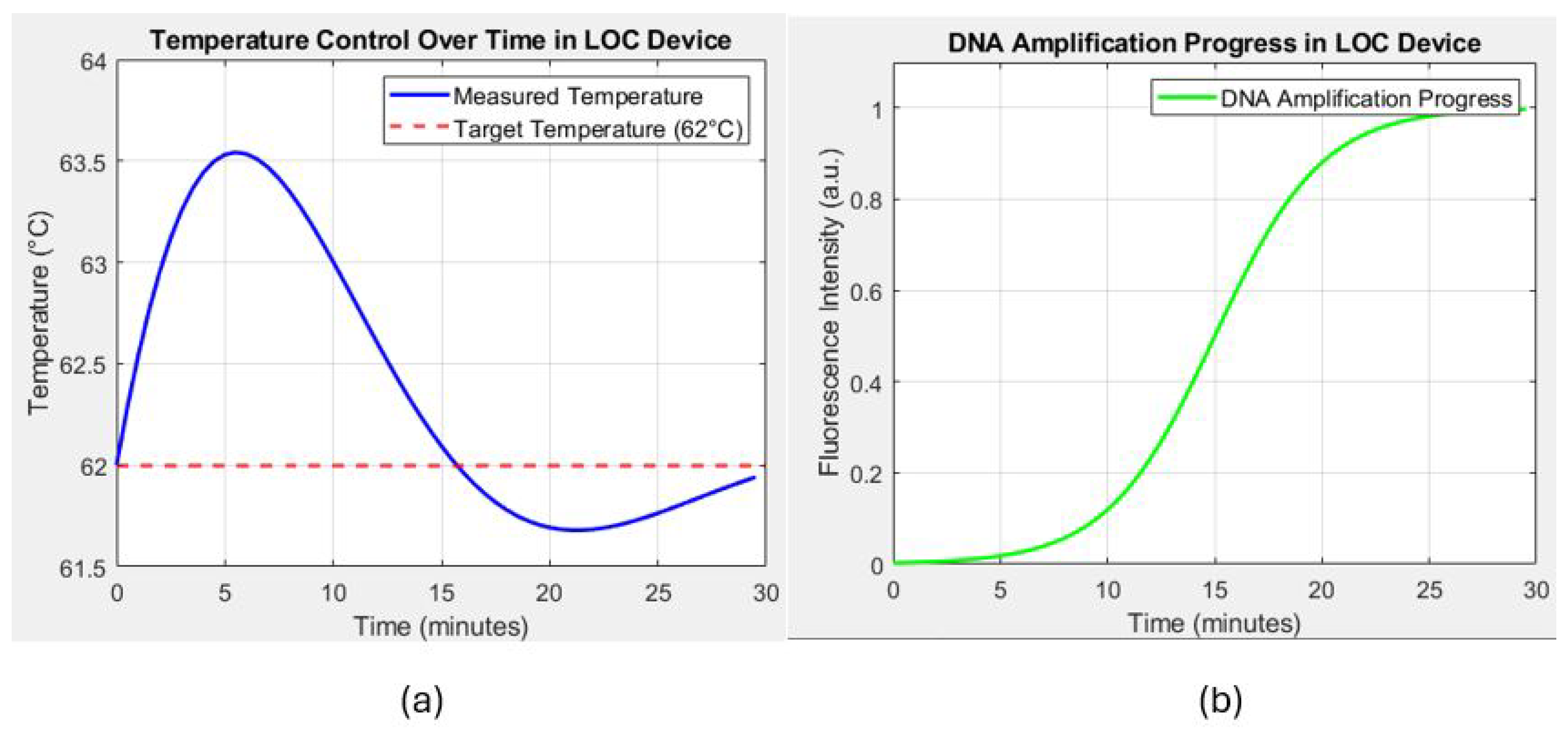
The thermal bed was tested with a real-time temperature monitoring setup using integrated optoelectronic sensors. Figure 12 (a) shows that the thermal bed rapidly reaches the target temperature of 62 °C within 2.5 seconds when a current of is applied. The measured temperature shows minor oscillations around the setpoint, indicating the control system’s effectiveness in maintaining a stable thermal environment. These oscillations were within C of the target temperature, demonstrating the precision of the temperature control system.
FEM simulations were conducted to predict the temperature distribution along the copper trace and validate the uniformity of the heating. Figure 12(a) illustrates the simulated temperature distribution at different intervals. The first half of the trace reaches the target temperature quickly, while the other half gradually heats up, confirming the expected thermal behavior of the system. The results indicate that the temperature distribution is highly uniform along the trace, with a deviation of less than throughout the length, even in a steady state.
The effectiveness of the thermal bed in facilitating DNA amplification was evaluated by monitoring the fluorescence intensity over time, which correlates with the DNA concentration during the amplification process. As depicted in Figure 12(b), the fluorescence intensity, representing the progress of DNA amplification, follows a typical sigmoid curve. This indicates successful DNA replication, with the amplification process nearing completion around the 25-minute mark. The sharp increase in fluorescence intensity between 10 and 20 minutes reflects the exponential phase of DNA replication, further demonstrating the thermal bed’s ability to maintain optimal conditions for rapid and efficient amplification.
The optoelectronic sensors integrated into the thermal bed played a crucial role in achieving precise temperature control and real-time monitoring of the DNA amplification process. The temperature sensor was calibrated to ensure accurate readings within the temperature range required for the -LAMP process. The calibration was verified through multiple trials, demonstrating a high correlation between sensor readings and reference temperatures, confirming the sensor’s reliability for real-time temperature monitoring. The colorimetric sensor, used to detect changes in the optical properties of the reaction mixture, was validated against known color standards. The sensor showed high sensitivity and specificity, detecting tiny color changes associated with DNA amplification. This capability is crucial to determine the endpoint of the amplification process without manual intervention.
The design efficiency of the thermal bed was evaluated based on its thermal response time, energy consumption, and compatibility with microfluidic systems. The thermal bed demonstrated a rapid thermal response, reaching the target temperature in less than 3 seconds. The thermal stability was maintained over extended periods, with minimal drift, essential for prolonged DNA amplification procedures. The design also allows for rapid cooling when required, making it adaptable for various thermal cycling protocols. The power consumption of the thermal bed was measured to be less than 1 W during steady-state operation, making it highly energy-efficient. This low power requirement is particularly advantageous for portable and battery-operated microfluidic devices, ensuring prolonged use without frequent battery replacements or recharges.
The results demonstrate the thermal bed’s suitability for integration into various microfluidic and lab-on-chip devices. Its ability to maintain precise temperature control and facilitate rapid DNA amplification has significant implications: the thermal bed can be used in point-of-care diagnostics for rapid pathogen detection, enhancing the speed and accuracy of disease diagnosis in clinical settings. The device’s also has the capability to detect and amplify DNA sequences can be applied to monitor biological safety in various environments, including food safety testing and environmental monitoring. The rapid and reliable DNA amplification facilitated by the thermal bed can help reduce processing times in forensic applications, particularly in analyzing crime scene samples and backlogged forensic cases.
DNA Amplification Progress: This graph represents the progress of DNA amplification over time, measured through the fluorescence intensity. The amplification follows a typical sigmoid curve, indicating successful DNA replication as the process progresses, which is detected by the increase in fluorescence intensity.
These results demonstrate the ability of the LOC device to maintain precise temperature control and effectively facilitate DNA amplification.
4. Discussion
The novel thermal bed design offers significant advantages over traditional thermal control systems used in DNA amplification. Using PCB copper traces and dielectric materials, the thermal bed provides a compact, modular, and repairable platform easily integrated into various microfluidic devices. Optoelectronic sensors enhance the system’s reliability and functionality, allowing for real-time monitoring and control of the amplification process.
The uniform temperature distribution and precise control achieved by the thermal bed are critical for the success of the -LAMP technology. Maintaining a stable thermal environment ensures high specificity and sensitivity in DNA amplification, making the thermal bed suitable for various applications in molecular diagnostics, including disease detection, biological safety monitoring, and forensic analysis.
The results of both experimental validation and simulations using the finite element method (FEM) demonstrate the efficacy and robustness of the proposed thermal bed design for DNA amplification using -LAMP technology. This discussion will explore the significance of these findings in the context of current technologies, the advantages and potential limitations of the design, and future directions for this research.
The novel thermal bed design using PCB copper traces and dielectric materials represents a significant advancement over traditional thermal control systems used in DNA amplification. Conventional systems often rely on bulkier heating elements, such as Peltier devices or resistive heaters, which can lead to uneven temperature distribution and increased energy consumption. In contrast, the proposed design offers several distinct advantages:
Enhanced Uniformity in Temperature Distribution: The FEM simulations and experimental data confirm that the thermal bed achieves a highly uniform temperature distribution throughout the copper trace, with deviations of less than . This is a critical improvement over existing systems, where temperature gradients can compromise the efficiency and accuracy of the amplification process.
Improved Energy Efficiency: With a power consumption of less than 1 W during steady-state operation, the thermal bed is substantially more energy-efficient than traditional heating. This low power requirement not only reduces operational costs but also makes the device suitable for portable, battery-operated applications, a significant benefit for point-of-care diagnostics.
Rapid Thermal Response: The ability to reach the target temperature of in 2.5 seconds demonstrates the rapid thermal response of the system. This quick response time is essential for reducing the overall processing time in DNA amplification, enabling faster diagnostic results compared to conventional systems that may require longer ramp-up and stabilization times.
The integration of optoelectronic sensors into the thermal bed design significantly enhances its functionality by providing real-time monitoring and control capabilities. The temperature sensor integrated into the system provides continuous feedback, allowing for precise control of the thermal environment. This real-time monitoring is crucial for maintaining the narrow temperature range required for optimal DNA amplification, reducing the risk of thermal fluctuations that could negatively impact the specificity and sensitivity of the process. The colorimetric sensor allows for the direct observation of DNA amplification progress by detecting changes in the optical properties of the reaction mixture. This capability not only simplifies the workflow by eliminating the need for external detection equipment but also enhances the accuracy of endpoint determination, which is crucial for applications requiring precise DNA quantification. The findings have significant implications for the future development of microfluidic and lab-on-chip devices. The modular design of the thermal bed allows for easy integration into various lab-on-chip configurations. Its scalability is advantageous for developing customized diagnostic platforms tailored to specific applications, such as infectious disease detection or genetic analysis. The potential to scale up production using standard PCB manufacturing techniques further supports its application in high-throughput.
5. Conclusions
We present a comprehensive approach to designing a novel thermal bed for temperature-controlled DNA amplification using optoelectronic sensors. The proposed thermal bed, constructed with PCB copper traces and dielectric materials, offers a precise and reliable temperature control crucial for the -LAMP process. The integration of optoelectronic sensors facilitates real-time monitoring and feedback control, significantly enhancing the system’s functionality and ensuring high specificity and sensitivity in DNA amplification.The experimental results and the finite element method (FEM) simulations confirm that the thermal bed maintains a stable thermal environment, which is essential to achieve consistent DNA amplification outcomes. The device’s ability to precisely control temperature in microfluidic settings makes it a versatile tool suitable for various applications in molecular diagnostics, including disease detection, biological safety monitoring, and forensic analysis.
Furthermore, the modular and repairable design of the thermal bed represents a significant advancement in lab-on-chip technologies, providing a versatile platform that can be easily adapted to other temperature-sensitive applications. Future work will focus on optimizing the response times of the thermal bed and exploring its scalability for mass production, potentially expanding its applicability in clinical and research settings. These developments underscore the potential for the integration of advanced thermal control systems and optoelectronic sensors into miniaturized diagnostic devices, paving the way for more efficient, reliable, and automated molecular diagnostics.
Author Contributions
conceptualization, H.T.O., M.S. and G.G.T. methodology, H.T.O., M.S. and G.G.T. software, R.E.M., and A.B.B.G. validation, R.E.M., and A.B.B.G. formal analysis, H.T.O. Investigation, H.T.O. resources, H.T.O and R.E.M. writing–original draft preparation, H.T.O., M.S., and G.G.T. writing–review and editing, H.T.O., M.S., and G.G.T. visualization, H.T.O., M.S. and G.G.T. supervision, M.S. and G.G.T. project administration, H.T.O and R.E.M. funding acquisition, H.T.O.and R.E.M.
Funding
This research received no external funding.
Conflicts of Interest
The authors declare no conflict of interest.
References
- Rodriguez, N.M.; Wong, W.S.; Liu, L.; Dewar, R.; Klapperich, C.M. A fully integrated paperfluidic molecular diagnostic chip for the extraction, amplification, and detection of nucleic acids from clinical samples. Lab Chip 2016, 16, 753–763. [Google Scholar] [CrossRef] [PubMed]
- Magro, L.; Escadafal, C.; Garneret, P.; others. Paper microfluidics for nucleic acid amplification testing (NAAT) of infectious diseases. Lab Chip 2017, 17, 2347–2371. [Google Scholar] [CrossRef] [PubMed]
- Yin, K.; Pandian, V.; Kadimisetty, K.; Ruiz, C.; Cooper, K.; You, J.; Liu, C. Synergistically enhanced colorimetric molecular detection using smart cup: a case for instrument-free HPV-associated cancer screening. Theranostics 2019, 9, 2637–2645. [Google Scholar] [CrossRef] [PubMed]
- Kundrod, K.A.; Barra, M.; Wilkinson, A.; others. An integrated isothermal nucleic acid amplification test to detect HPV16 and HPV18 DNA in resource-limited settings. Sci Transl Med 2023, 15, eabn4768. [Google Scholar] [CrossRef] [PubMed]
- Zamani, M.; Furst, A.L.; Klapperich, C.M. Strategies for Engineering Affordable Technologies for Point-of-Care Diagnostics of Infectious Diseases. Acc Chem Res 2021, 54, 3772–3779. [Google Scholar] [CrossRef]
- El-Ali, J.; Sorger, P.K.; Jensen, K.F. Cells on chips. Nature 2006, 442, 403. [Google Scholar] [CrossRef]
- Dittrich, P.S.; Tachikawa, K.; Manz, A. Micro total analysis systems. Latest advancements and trends. Analytical chemistry 2006, 78, 3887–3908. [Google Scholar] [CrossRef]
- Whitesides, G.M. The origins and the future of microfluidics. Nature 2006, 442, 368. [Google Scholar] [CrossRef]
- Li, D. Encyclopedia of microfluidics and nanofluidics; Springer Science & Business Media, 2008.
- Wu, L.L.; Babikian, S.; Li, G.P.; Bachman, M. Microfluidic printed circuit boards. 2011 IEEE 61st electronic components and technology conference (ECTC). IEEE, 2011, pp. 1576–1581.
- De Bourcy, C.F.; De Vlaminck, I.; Kanbar, J.N.; Wang, J.; Gawad, C.; Quake, S.R. A quantitative comparison of single-cell whole genome amplification methods. PloS one 2014, 9, e105585. [Google Scholar] [CrossRef]
- Luka, G.; Ahmadi, A.; Najjaran, H.; Alocilja, E.; DeRosa, M.; Wolthers, K.; Malki, A.; Aziz, H.; Althani, A.; Hoorfar, M. Microfluidics integrated biosensors: A leading technology towards lab-on-a-chip and sensing applications. Sensors 2015, 15, 30011–30031. [Google Scholar] [CrossRef]
- Lakssir, B.; Benhassou, H.A. ; others. A Lab-On-Card for a point of care infectious disease diagnosis. 2016 6th Electronic System-Integration Technology Conference (ESTC). IEEE, 2016, pp. 1–3.
- Zhang, R.; Qin, J.; Tian, H.; Si, W.; Wang, T.; Liu, Z. Study on DNA electrochemical behavior for label-free micro PCR application. 2011 6th IEEE International Conference on Nano/Micro Engineered and Molecular Systems. IEEE, 2011, pp. 952–955.
- Varapula, D.; Gutta, S.; Mauk, M.; Liu, C. A highly-simplified nucleic-acid microfluidic test device based on capillary wicking action for point-of-care diagnostics. 2015 41st Annual Northeast Biomedical Engineering Conference (NEBEC). IEEE, 2015, pp. 1–2.
- Collings, A.; Caruso, F. Biosensors: recent advances. Reports on Progress in Physics 1997, 60, 1397. [Google Scholar] [CrossRef]
- Hilvert, D. Critical analysis of antibody catalysis. Annual review of biochemistry 2000, 69, 751–793. [Google Scholar] [CrossRef] [PubMed]
- Cheng, A.K.; Ge, B.; Yu, H.Z. Aptamer-based biosensors for label-free voltammetric detection of lysozyme. Analytical chemistry 2007, 79, 5158–5164. [Google Scholar] [CrossRef] [PubMed]
- Singh, M.; Kathuroju, P.K.; Jampana, N. Polypyrrole based amperometric glucose biosensors. Sensors and Actuators B: Chemical 2009, 143, 430–443. [Google Scholar] [CrossRef]
- Chang, W.H.; Wang, J.H.; Ling, W.S.; Cheng, L.; Wang, C.H.; Wang, S.W.; Lee, G.B. An intergated microfluidic system for detecting human immunodeficiency virus in blood samples. 2013 IEEE 26th International Conference on Micro Electro Mechanical Systems (MEMS). IEEE, 2013, pp. 903–906.
- Safavieh, M.; Ahmed, M.U.; Zourob, M. High throughput low cost electrochemical device for S. aureus bacteria detection. SENSORS, 2013 IEEE. IEEE, 2013, pp. 1–4.
- Choi, G.; Song, D.; Miao, J.; Cui, L.; Guan, W. Mobile all-in-one malaria molecular diagnosis for field deployment in resource-limited areas. 2016 IEEE Healthcare Innovation Point-Of-Care Technologies Conference (HI-POCT). IEEE, 2016, pp. 212–215.
- Lao, A.I.; Lee, T.M.; Hsing, I.M.; Ip, N.Y. Precise temperature control of microfluidic chamber for gas and liquid phase reactions. Sensors and Actuators A: Physical 2000, 84, 11–17. [Google Scholar] [CrossRef]
- Sun, Y.; Wang, X.; Wang, K.; Ma, X.; Zeng, Y. A Programmable Thermal Controlling Array for Microfluidic Lab-On-A-Chip Systems. 2007 1st International Conference on Bioinformatics and Biomedical Engineering. IEEE, 2007, pp. 1230–1233.
- Babikian, S.; Wu, L.; Li, G.; Bachman, M. Microfluidic thermal component for integrated microfluidic systems. 2012 IEEE 62nd Electronic Components and Technology Conference. IEEE, 2012, pp. 1582–1587.
- Zheng, Y.; Sawan, M. Planar microcoil array based temperature-controllable lab-on-chip platform. IEEE Transactions on Magnetics 2013, 49, 5236–5242. [Google Scholar] [CrossRef]
- Scorzoni, A.; Tavernelli, M.; Placidi, P.; Valigi, P.; Nascetti, A. Accurate analog temperature control of a thin film microheater on glass substrate for lab-on-chip applications. SENSORS, 2014 IEEE. IEEE, 2014, pp. 1216–1219.
- Scorzoni, A.; Tavernelli, M.; Placidi, P.; Zampolli, S. Thermal modeling and characterization of a thin-film heater on glass substrate for lab-on-chip applications. IEEE Transactions on Instrumentation and Measurement 2014, 64, 1098–1098. [Google Scholar] [CrossRef]
- Streit, P.; Nestler, J.; Shaporin, A.; Schulze, R.; Gessner, T. Thermal design of integrated heating for lab-on-a-chip systems. 2016 17th International Conference on Thermal, Mechanical and Multi-Physics Simulation and Experiments in Microelectronics and Microsystems (EuroSimE). IEEE, 2016, pp. 1–6.
- Petrucci, G.; Caputo, D.; Nascetti, A.; Lovecchio, N.; Parisi, E.; Alameddine, S.; de Cesare, G.; Zahra, A. Thermal characterization of thin film heater for lab-on-chip application. 2015 XVIII AISEM Annual Conference. IEEE, 2015, pp. 1–4.
- Osawa, Y.; Katsura, S. Temperature control on a curved surface for implementing to wearable interfaces. IECON 2016-42nd Annual Conference of the IEEE Industrial Electronics Society. IEEE, 2016, pp. 348–353.
- Gonzalez, I.O.B.; Perez, R.R.; Batlle, V.F.; Fernandez, L.P.S.; Perez, L.A.S. Fuzzy gain scheduled Smith predictor for temperature control in an industrial steel slab reheating furnace. IEEE Latin America Transactions 2016, 14, 4439–4447. [Google Scholar]
- Martinez-Quijada, J.; Caverhill-Godkewitsch, S.; Reynolds, M.; Sloan, D.; Backhouse, C.J.; Elliott, D.G.; Sameoto, D. Deterministic Design of Thin-Film Heaters for Precise Spatial Temperature Control in Lab-on-Chip Systems. Journal of Microelectromechanical Systems 2016, 25, 508–516. [Google Scholar] [CrossRef]
- Stojkovic, M.; Uda, N.R.; Brodmann, P.; Popovic, M.; Hauser, P.C. Determination of PCR products by CE with contactless conductivity detection. Journal of separation science 2012, 35, 3509–3513. [Google Scholar] [CrossRef]
- Liu, Z.; Zhang, R.; Guo, C.; Qin, J.; Tian, H.; Si, W.; Wang, T. Integration of micro-PCR with CMOS EC detection: Opportunity and challenges. 2011 6th IEEE International Conference on Nano/Micro Engineered and Molecular Systems. IEEE, 2011, pp. 1200–1203.
- Bumiller, E.; Hillman, C. A review of models for time-to-failure due to metallic migration mechanisms. DFR Solutions white paper 2009. [Google Scholar]
- Bergman, T.L.; Incropera, F.P.; DeWitt, D.P.; Lavine, A.S. Fundamentals of heat and mass transfer; John Wiley & Sons, 2011.
- Scholl, M.S.; Wolfe, W.L. Infrared target design: fabrication considerations. Applied optics 1981, 20, 2143–2152. [Google Scholar] [CrossRef] [PubMed]
- Scholl, M.S. Thermal considerations in the design of a dynamic IR target. Applied optics 1982, 21, 660–667. [Google Scholar] [CrossRef] [PubMed]
- Scholl, M.S. Spatial and temporal effects due to target irradiation: a study. Applied optics 1982, 21, 1615–1620. [Google Scholar] [CrossRef]
- Chaber, P.; awryńczuk, M. Effectiveness of PID and DMC control algorithms automatic code generation for microcontrollers: Application to a thermal process. 2016 3rd Conference on Control and Fault-Tolerant Systems (SysTol). IEEE, 2016, pp. 618–623.
- Haiyang, Z.; Yu, S.; Deyuan, L.; Hao, L. Adaptive neural network PID controller design for temperature control in vacuum thermal tests. 2016 Chinese Control and Decision Conference (CCDC). IEEE, 2016, pp. 458–463.
- Said, M.; Shalaby, A.; Gebali, F. Thermal-aware network-on-chips: Single-and cross-layered approaches. Future Generation Computer Systems 2019, 91, 61–85. [Google Scholar] [CrossRef]
Figure 1.
Block diagram illustrating the sensors and hardware interconnections within the Lab-On-Chip (LOC) system. The diagram shows how a microprocessor coordinates the communication between sensors and a computer using standard communication protocols, enabling precise control and monitoring of the DNA amplification process.
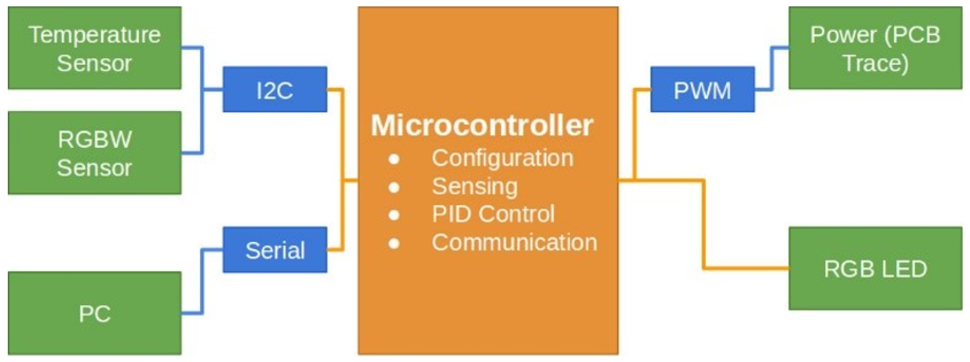
Figure 2.
Characteristics of the PCB used in the design of the thermal bed. (a) Cross-sectional view of the copper trace on the substrate material, illustrating the physical dimensions and layout of the trace. (b) Graph showing the relationship between electric current and the transverse cross-sectional area of the copper trace for various final temperature increments under a 1 W power source. The graph demonstrates temperature increases from 10 °C to 100 °C in 10 °C intervals, highlighting the thermal response characteristics of the copper trace.
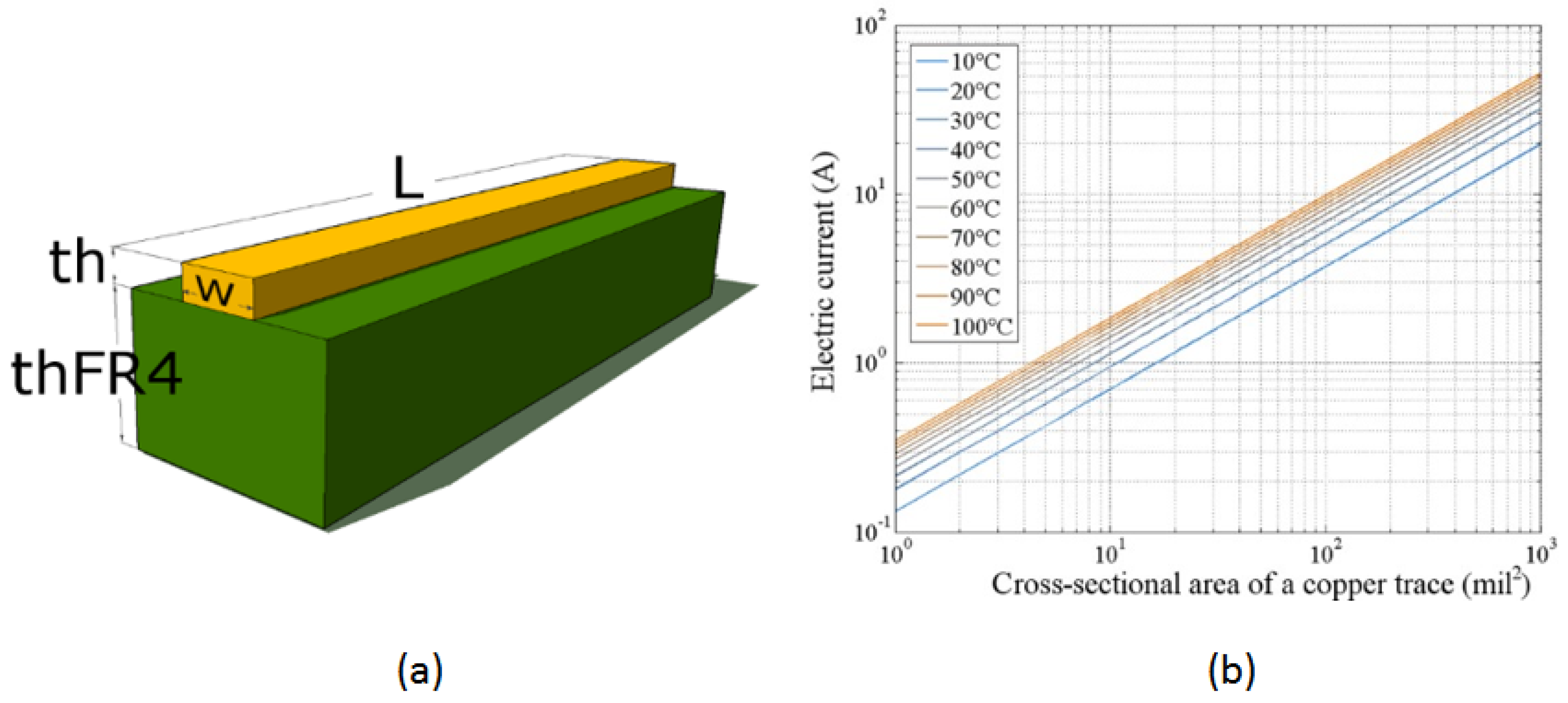
Figure 3.
Sketch used to model the thermal energy transport along the copper trace and the calibration curve of temperature as a function of electrical current. (a) Geometry used to determine the energy flow balance through a segment of the copper trace at a specific moment in time. The resistive losses generate heat as electrical current flows through the copper trace, resulting in a temperature increase. There is no external thermal input or output energy in this model. (b) Temperature as a function of electrical current for the copper trace in the PCB, showing an approximately quadratic relationship.
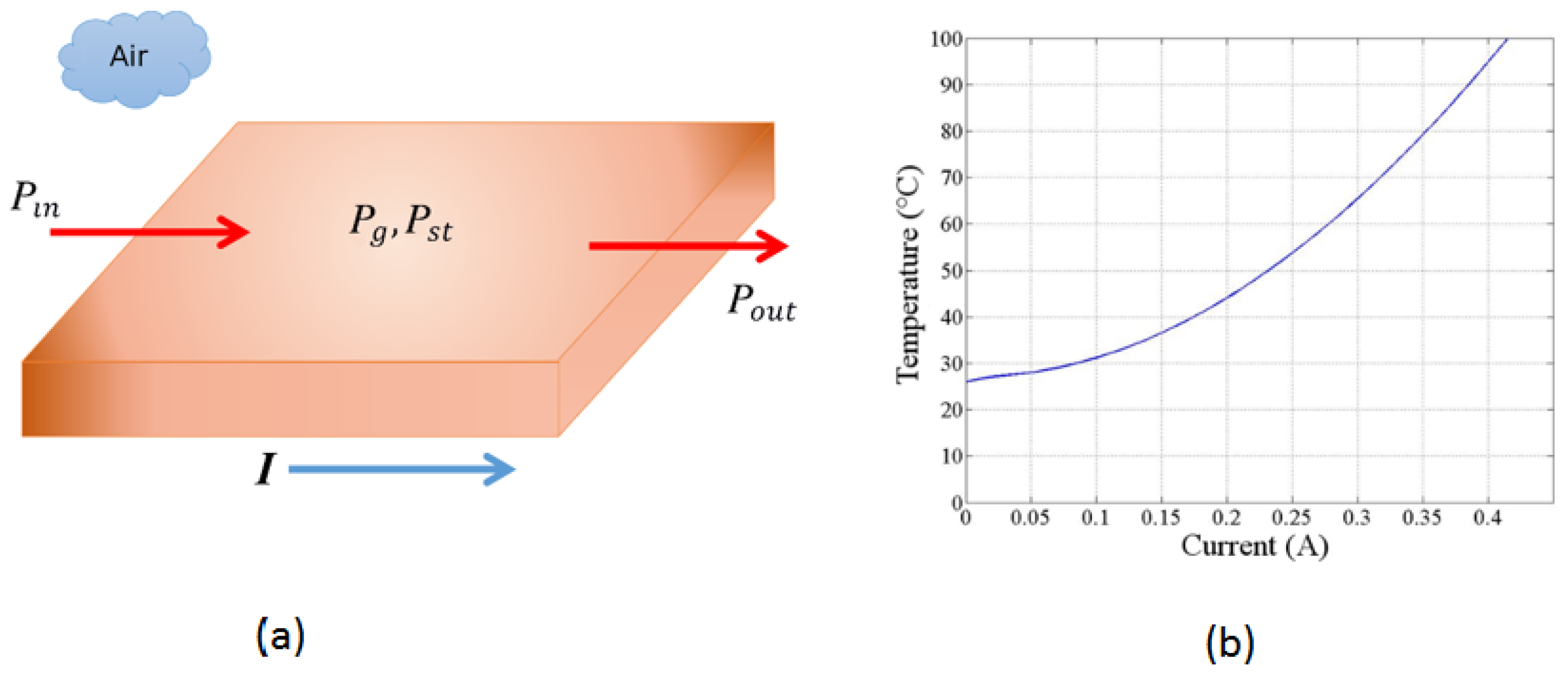
Figure 4.
Two schemes of the PCB trace analyzed using the finite element method (FEM). (a) The dynamic mesh suitable for FEM, showing the geometric layout of the copper trace. The mesh density increases in areas of greater interest, such as corners, to enhance the accuracy of the analysis. (b) The vector current density as a function of location on the trace, indicating how electrical current is distributed along the copper trace.
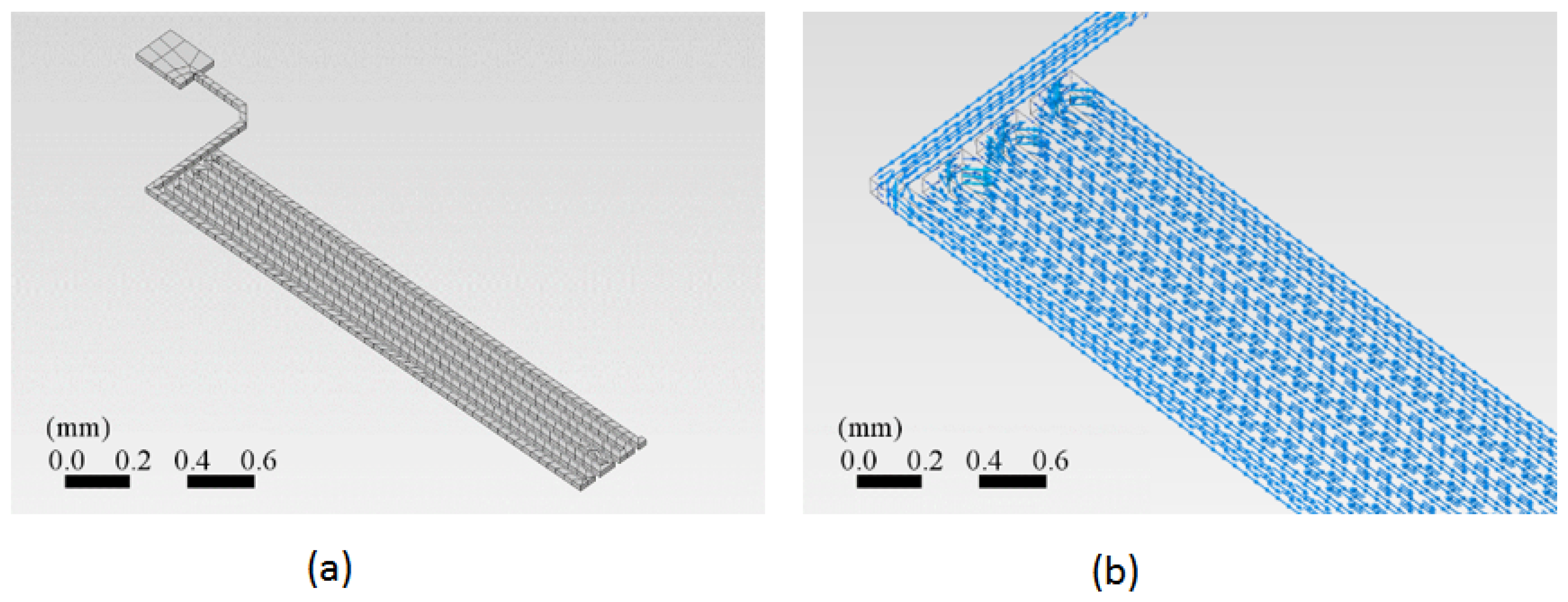
Figure 5.
Geometrical and current density parameters of the PCB trace. (a) The geometrical configuration of the copper trace shows the reference potential points and motion anchoring positions used in the analysis. (b) The electric current density vectors as a function of location on the trace surface. The color scale on the right indicates current density values, ranging from 0 to A m−2. The current density magnitude is highest where the trace bends at a 90 °C.
Figure 6.
Temperature distribution in the copper trace starting from an initial temperature of 25 °C. (a) At 0.5 seconds after a current of 0.5 A is applied, the first half of the trace has begun to heat, while the end segment remains at room temperature, as indicated by the darker blue color. (b) At 2.5 seconds with the same current of 0.5 A, the first half of the trace has reached the target temperature of 62°C, while a portion of the trace still remains at room temperature, represented by the blue color.
Figure 7.
Design of the thermal stage using the EAGLETM CAD program. (a) The layout of the upper layer shows the arrangement of copper traces designed to ensure optimal uniformity when heating the sample chamber. (b) The layout of the lower layer illustrates a similar trace arrangement to maintain uniform heating throughout the sample chamber.
Figure 8.
Block diagram of the PID control system implemented in the DNA amplification device. The PCB (plant) is modeled as an RLC circuit to represent the resistive (R), inductive (L), and capacitive (C) components of the thermal control system. This model allows precise regulation of the temperature within the device to ensure optimal conditions for DNA amplification.
Figure 9.
(a) The temperature response programmed in the controller using the proposed thermal model. The blue line represents the reference signal, scaled and expressed in temperature units, showing how the system tracks the desired setpoint. (b) The simulated control signal for the system demonstrates the initial peak with a saturation limitation due to the sharp change from a high-step input. This peak behavior results from the control system’s attempt to reach the target temperature rapidly.
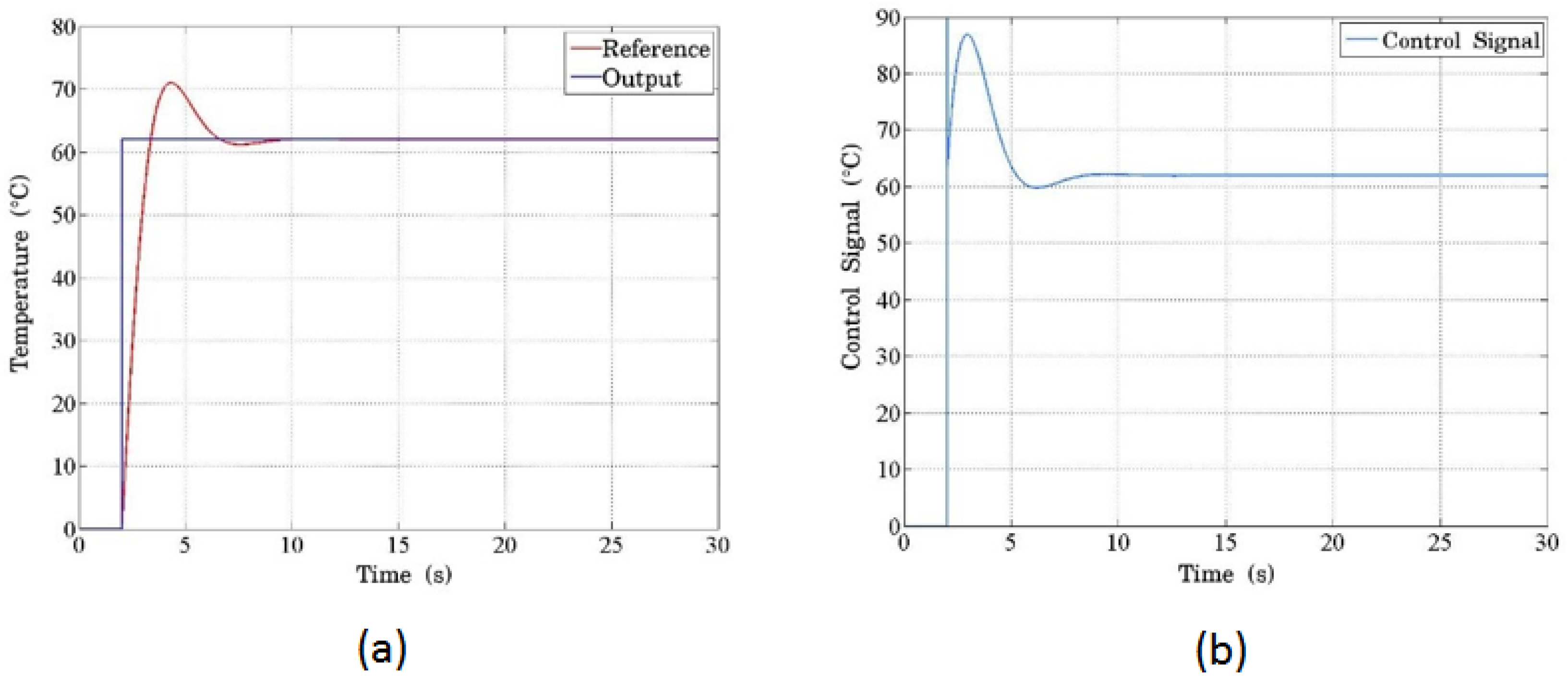
Figure 10.
A photo of the assembled control systems for the DNA amplification device. (a) The primary PCB control unit, showing the main components responsible for regulating temperature and system operations. (b) The secondary control PCB with a protective cover, which houses additional circuitry for managing the device’s sensor inputs and outputs.
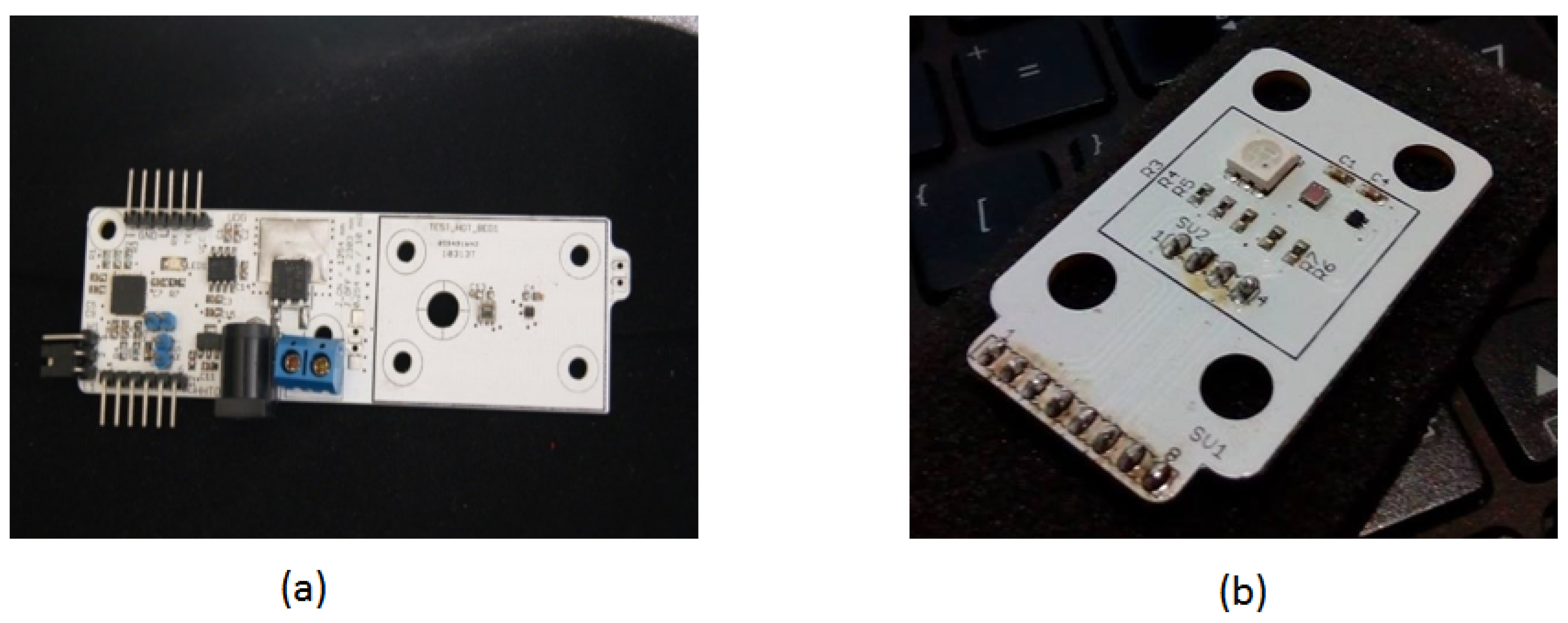
Figure 11.
PCB layout design for the DNA amplification device control unit. (a) Top view of the primary PCB control layout, showing the placement of components and copper traces for optimal performance. (b) Bottom view of the primary PCB control layout, illustrating the routing of connections and additional components to ensure reliable operation of the control system.
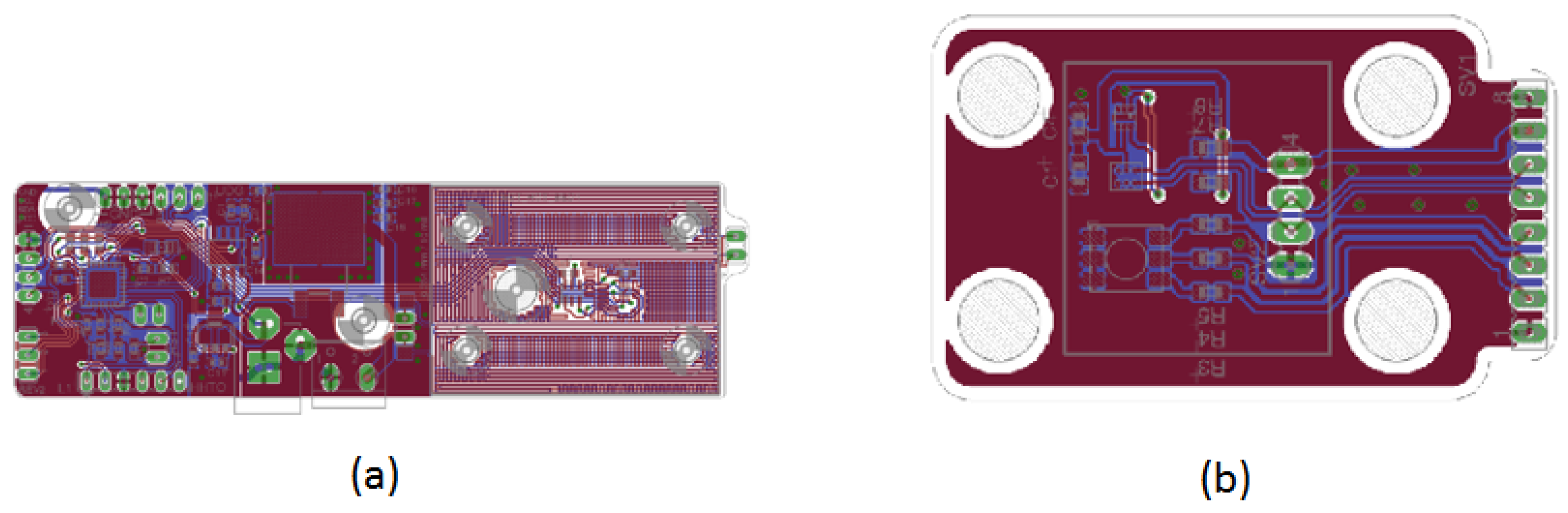
Figure 12.
(a) Temperature control over time in the Lab-On-Chip (LOC) device, showing the measured temperature (blue line) and the target temperature (C, red dashed line). The graph demonstrates the ability of the device to maintain a stable temperature around the target setpoint, which is critical for effective DNA amplification. (b) Progress in DNA amplification in the LOC device, represented by the fluorescence intensity over time (green line). The sigmoid curve indicates the successful amplification of DNA, with the process nearing completion around the 25-minute mark
Disclaimer/Publisher’s Note: The statements, opinions and data contained in all publications are solely those of the individual author(s) and contributor(s) and not of MDPI and/or the editor(s). MDPI and/or the editor(s) disclaim responsibility for any injury to people or property resulting from any ideas, methods, instructions or products referred to in the content. |
© 2024 by the authors. Licensee MDPI, Basel, Switzerland. This article is an open access article distributed under the terms and conditions of the Creative Commons Attribution (CC BY) license (http://creativecommons.org/licenses/by/4.0/).
Copyright: This open access article is published under a Creative Commons CC BY 4.0 license, which permit the free download, distribution, and reuse, provided that the author and preprint are cited in any reuse.


