Submitted:
26 August 2024
Posted:
27 August 2024
You are already at the latest version
Abstract
This paper evaluates the open and closed loop DC-DC converter operation within a DC coupling multilevel inverter architecture to obtain an infinite level stepped sinusoidal voltage. Adding a cascade controller to the DC-DC converter should reduce the settling time and increase the number of levels in the output voltage waveform, it could decrease the speed error and phase shift concerning the sinusoidal reference signal. The proposed methodology consists of implementing an experimental multilevel inverter with DC coupling, through a single-phase bridge inverter energized from a BUCK converter, trigger signals for the two converters are obtained from a control circuit based in an ATMEGA644P microcontroller, and a digital controller is also implemented to evaluate the operation of the BUCK converter in open and closed loop and observe its influence in the stepped sinusoidal output voltage. The evaluation is performed to energize a resistive load with common output voltage in multilevel inverters, that is 3, 5, 7, 11, and infinity levels. Results show that during the design stage, fast dynamic elements, like the storage capacitor, can be used to obtain a minimum THD because the settling time is sufficiently fast and the speed error remains small and there isn’t a need for a controller. A digital controller requires processing time and although in theory, it can reduce the settling time to a minimum, the processor introduces latency in the control signals generation, producing the opposite effect. Controller complexity of the digital controller must be considered because it increases processing time and influences the efficiency of the closed-loop operation.
Keywords:
Multilevel inverter
; Infinite level inverter
; Buck converter
; Open loop
; Closed loop
1. Introduction
At present, electrical energy from renewable energy sources is one of the main research topics, especially the use of solar energy captured by photovoltaic panels. To integrated this systems into the electrical power system, it is necessary to use an inverter, power converters that allow obtaining an AC voltage from a DC voltage; the simplest and most commonly used topology is known as PWM inverter, it produces a square voltage waveform where the fundamental sinusoidal component predominates. The disadvantage of this topology is the harmonic content with a THD of 48.43%. Modulation strategies improve the pwm inverter output such as sinusoidal pulse width modulation (SPWM), which reduces the harmonic content with a THD of 41% and allows voltage amplitude control, however, it increases switching losses, limiting the switching frequency [1]. THD is an importan factor in High power applications, harmonics can generate undesired operation effects, electromagnetic interference, low efficiency, In Figure 1 the output waveform and frequency spectrum of a PWM and SPWM inverter are showed, the difference in the harmonic content can be appreciated.
Multilevel inverter topologies can deal with these drawbacks, they have a topology in which a stepped voltage waveform is obtained and a low harmonic content can be reached because the waveform is more similar to a sinusoidal. The THD can be controlled with the quantity of levels, it can be said that more levels less THD. [2]
The stepped voltage waveform is obtained with energy bank implemented with series connected capacitors to provide nodes where controlled switches are connected. Each capacitor has a voltage according to Equation (1), where m represents the number of levels or accesible nodes form tue energy bank .
A conceptual topology is showed in Figure 2, the stepped voltage waveform is generated from each energy bank node to a reference node , if the positive half period output waveform is generated when switching from to and return to with appropiate control signals. The negative half period is generated in opposite way when and switching starts in [3]. In Figure 2 the output voltage waveform is showed.
The harmonic distorsion can be reduced with a high number of voltage level in the waveform, Figure 3 shows the harmonic spectre in a nine level inverter. Compared to the harmonic spectre in Figure 1, a considerable reduction in the number of harmonics and its amplitude can be noted, without the need to use a modulation technique.
Multilevel inverter topologies seek to use low breakdown voltage power switches in high voltage applications, commonly used topologies are clamping diode, floating capacitor and cascaded inverters, the first two topologies require a large number of power switches, in addition to other electronic components whose number will increase depending on the number of levels in its output, additionally they introduce static and dynamic unbalances in the blocking voltages of each device, so external damping networks must be added to equalize the blocking voltages. Single-phase cascaded inverters present a similar disadvantage in terms of the number of components, however, they present an easier implement design, but the control of each inverter must be adjusted each time that change the number of output voltage levels. In general terms, a multilevel AC waveform increases the amount of static and dynamic losses in power converters, so it is common implement inverters of 15 levels as maximum. In Table 1 the electric components number is showed, it can be noted that the higher the number of levels, the more complex the circuit becomes in the number of devices as well as the control [5].
In [7] a clamping diode configuration is used, where THD values of 28.58% are obtained using a 5-level inverter. Tests are performed where the THD decreases to a value of 2.53% when using a 15-level inverter implemented with 28 switches per phase. [8] implements a basic unit of a switched capacitor topology utilizing a cascaded H-bridge to generate 13 and 31 level output voltage with a lower number of components, a THD 0f 2.63% was achieved. [9] shows a cascaded module configuration where the number of switches will be for levels at the output, the THD obtained for an 11-level configuration (12 static switches in the bridge) is 8.61%. These works evidence the use of a large number of semiconductor elements, moreover, in three-phase systems the number of semiconductors triples and requires the use of complex controllers running extensive algorithms.
In [10,11,12] a topology called inifinite level inverter (ILI) is proposed, where a DC-DC converter is cascaded with a single-phase full-bridge inverter. This topology is mentioned in [13] as variable inverter with DC link, a stepped wave can be obtained by controlling the output voltage of the DC-DC converter while the inverter switches its switches in conduction at 180° A topology scheme is showed in Figure 4. Through this type of operation, an infinite-level inverter can be obtained where several levels can be reached with fewer electronic devices, reducing losses, costs, size, complexity and increasing efficiency.
In [14,15] a buck-type step-down DC-DC converter with variable duty ratio in steps according to a sampled sine wave is used as a DC link, generating at the inverter output a step wave with a THD of 2.36% at a switching frequency of 10 KHz. Similar results are obtained in [16] with a THD of 1.2% and 98% efficiency in an evaluation with resistive load. In [17,18] a buck-boost converter is used to make more efficient use of the DC voltage at the input of the converter. In these works there is no voltage feedback so the levels depend exclusively on the reference signal generated, and can be affected by disturbances, introducing distortion in the output voltage waveform. In the case of [18] a THD that varies from 2% to 8.20% depending on the load associated with the circuit at a switching frequency of 10KHz is obtained. [19] presents a novel topology to develop a three phase infinite level inverter, it use less semiconductors than traditional inverter topologies and in combination with third harmonic injectio PWM technique can achieve a THD of 0.39%.
ILI has been investigated in applications such as motor management, voltage restoration and reactive compensation, in all these works the inverter works in open loop and the transient response to disturbances is not evaluated [16,20,21]. For Infinite levels operation, the DC-DC converter output voltage must follow a sinusoidal signal reference, being necessary to consider the dynamics of the DC-DC converter, which has been little or nothing explored. If there is a speed error, there will be a phase shift in the inverter voltage signal, which would complicate control signals synchronization, especially if it works integrated into a power electrical system (PES). Also a poor transient response could result in a poor response to disturbances or primary control strategies within a PES [22,23,24,25].
Power converters in closed loop could improve its dynamic response in time and over impulse throught a controller [26]. There are some works that include a cascade controller in DC-DC converters such as [22,27,28], they implements PID, GPI and H∞ controllers on high-end processors such as DSP and FPGA, GPI controller presents a lower settling time compared to PID, vs. respectively. In addition, GPI control shows an output shorter recovery time against sudden RL load switching and showed a higher noise decrease in the response. H∞ controller has adaptive characteristic as it changes the parameter based on the degree of error present in the output, this controller obtains a settling time of .
Modern control straegies have been explored in DC-DC converters, [29] implements a Particle Swarm Optimization (PSO) algorithm to tune PID controller parameters and compared it with conventional Ziegler-Nichols method. Investigation concludes that the latter strategie provides a better dynamic response, however, it is noted that this technique is effective as long as system parameters like input voltage and load don’t change too much. Algorithms such as SMC (Sliding Mode Control) implemented in [30] are a good nonlinear control strategy applied to power converters, it presents better performance compared to a dual-loop PI controller. Complex control algorithms require higher computational load, requiring complex control systems to improve system robustness but slowing down dynamic response.
In this article a monophasic multilevel inverter with DC-DC link is implementes trought a single-phase full-bridge inverter energized from a Buck converter, it includes closed loop operation in the BUCK converter, the contribution given is the analysis of closed loop operation to reduce the speed error and provide immunity to disturbances, compared with open loop operation in order to determine the suitability or not of this operation mode.
2. Materials and Methods
To evaluate the open and closed loop operation of the DC-DC converter in an infinite-level inverter topology, an experimental electronic circuit is implemented according to Figure 5. To obtain results that can be contrasted with the work of [12] and [31], the circuit is able to deliver an output voltage of for a resistive load of . Considering the load, a single phase full bridge inverter is implemented with a maximum input voltage of ; for the DC-DC converter the BUCK topology is used with an input voltage of from a DC source, voltages between and can be obtained according to the duty cycle control. Switching frequency is selected considering [32], it should be between to , however taking as reference the work of [18] that compares several works related to multilevel waves using BUCK and BOOST topologies, switching frequency is stablished in 40 KHz.
2.1. BUCK Converter Stage
According to Figure 5, Buck converter design has two stages, firstly, capacitor and inductor are selected to define an output voltage ripple and inductor current ripple; secondly, power switches () are dimensioned to tolerate blocking voltages and conduction currents. Design conditions are showed in Table 2.
L and C are calculated with Equations (2) and (3) [33]. A toroidal inductor of and an output capacitor of are selected. Equations (4), (5), (6) and (3) are used for dimension diode and Mosfet [33], a Hiperfast BYC15-600 diode is used in D, which due to its high switching speed reduces associated Mosfet dynamic losses. is a MOSFET IRFP460A, whose high speed and low dynamic losses make it ideal for Switched Mode Power Supply applications.
2.2. Single-Phase Full Bridge Inverter Stage
A single phase full bridge inverter design consist in power switches dimensioning to tolerate blocking voltages and conduction currents with Equations (8) and (9). Power switches , , and are IGBT’s model K75H603, which is a high-speed switch model ideal for power converter applications.
For a proper IGBT triggering it is necessary to use a coupling circuit for the controller signals, HCPL 3120 is used as indicated in the figure is a high speed optocoupler that serves to isolate the control stage from the power stage and its output is adequate for IGBT trigger, HCPL 3120 is used as indicated in Figure 6.
2.3. Controller
Controller is the logic circuit that generates PWM signals to trigger power switches in the DC-DC converter and inverter, in open and closed loop operation. The control program is implemented in an ATMEGA644 microcontroller and an ADC0804 digital analog converter with a voltage divider is used for feedback the BUCK output voltage. Figure 7 shows used elements and their connections.
The developed program allows to choose the number of levels for the inverter output voltage waveform, then the value of the BUCK PWM duty ratio and its duration is calculated using the number of levels ans output frequency. For the full-bridge inverter, a PWM with duty ratio of 50% is generated, it remains constant all the time. In closed-loop operation, the BUCK output voltage error is calculated and execute the compensator routine to control the BUCK duty ratio; a program flowchart can be seen in Figure 8.
2.4. Digital Compensator
To improve the DC-DC converter dynamics, a PID compensator is used, taking into account that the position error will be cancelled and there will be fast response to disturbances as the change of reference by a sinusoidal relationship. Figure 9 shows a compensator schematic and Equation (9) and (11) describe mathematically the compensator in time domain, where E is the voltage error, while U is the BUCK converter pulse width value; KP, KI and KD represent proportional, integral and derivative constants that determine the compensator behavior [33].
To implement the compensator digitally and to establish a controller programming routine, (9) is discretized using bilinear transform with s to z relationship by Equation (12), digital PID difference equation is given by Equation (13) and compensator constants are determined by Equations (14), (15) and (16).
Compensator constants are obtained experimentally by classical tuning using Ziegler-Nichols. Constants have been adjusted to obtain the best transient response, the fastest response with the lowest overshoot is obtained with , y .
3. Results
To obtain data for open and closed loop evaluation of the BUCK converter within the infinite level inverter, the circuit described in the section is implemented, the output voltage is analyzed and recorded using an oscilloscope, with numerical storage capability, and then the data is analyzed with the FFT powergui tool of the simscape library of MATLAB R2023b, Figure 10 shows the implemented hardware.
First open-loop operation is evaluated to form a sine wave of infinite levels, for this duty ratio varies with for a complete period. A square waveform is obtained because the BUCK converter presents a slow dynamics, with a settling time () of . According to [18], the depends on equation 17, so the value of C is modified, the results are synthesized in Figure 11, where it can be appreciated that with a sine wave is obtained and . BUCK converter for an infinite level inverter must be designed with a low capacitance and so that this doesn’t affect ripple, it must be designed with a small value of .
The operation is evaluated with for C, to form a stepped waveform of 3,5,7 and 9 levels. Obtained results can be seen in Figure 12, where it is possible to appreciate the ripple presence in the levels of the stepped wave, this is due to the low value of capacitance.
Each wave is analyzed in MatLab to determine the distortion, obtaining the values shown in Table 3, where a decrease in the harmonic content with respect to the increase of levels can be appreciated, obtaining a distortion for infinite levels and increasing to for three levels. In the case of infinite levels, a low harmonic content in the third harmonic and less than for the rest. THD percentage value obtained for infinite levels is within the ranges allowed by IEEE std.519 for low voltage applications.
Before evaluating the infinite-level inverter closed-loop operation, isolated BUCK converter closed-loop is evaluated to observe the compensator influence. The test is performed for four reference values , , and . A comparison between open-loop and closed-loop dynamics is performed with the test results as can be seen in Figure 13.
For each reference value the maximum over impulse , settling time and rise time are measured. To measure , 10% criterion is taken into account while is measured between 10% and 90% of the voltage final value. For the , the maximum value of the response is compared to the steady-state response value in uderdamped response. Measured parameters for the four scenarios are shown in Table 4. There is an improvement in the for closed loop operation, as the settling time is reduced with larger reference change. The designed compensator allows to reduce steady state error so that in closed loop is maximum , while in open loop the errors reaches for reference variations from to .
Finally closed-loop operation of the infinite level inverter is evaluated, the evaluation conditions are the same as in the open-loop test in order to contrast the results. Results obtained can be seen in Figure 14, where a frequency of 60 Hz is achieved for the fundamental. When there is an increase of levels there is not a considerable improvement in THD as can be seen in Table 5. The best result is presented for 3 levels with a THD of 33.51% which increases to 58.04% for infinite levels. The infinite level test measures a high presence of odd and even harmonics, so the resulting voltage waveforms have high THD and asymmetry values. As in open-loop, output voltage waves present peaks due to the low value of C and it can be said that due to the fast dynamics in open-loop, the compensator does not help to improve the THD, compensator introduces latency in the inverter operation.
Additionally, Compensator behavior with 2200 uF in the BUCK converter output was evaluated, results shows that it isn’t possible to generate an output voltage with frequencies in 50Hz to 60Hz range, due to the converter slow dynamics. Changes in the reference at frequencies close to 60Hz generate system instability due to the output capacitor charging and discharging times. The frequencies generated under these test parameters allowed to generate alternating voltage waves at the output frequency up to and a THD of 14.24% in the best case, there are no voltage peaks and compensator improve the transient, these results can be seen in Figure 15 .
4. Conclusions
Open-loop test results are better than closed-loop tests results, open-loop harmonic distortion of 3.47% was obtained, which is a distortion value accepted by IEEE std 519 in low voltage applications, on the other hand, closed-loop showed high levels of harmonic distortion as well as the presence of even harmonics revealing a low quality in the output voltage waveform generated. This shows that for an infinite level inverter designed with a fast dynamic DC-DC converter it is not convenient to close the loop with the DC output voltage, as future research would be to evaluate the behavior by closing the loop with the rms voltage at the inverter output.
The use of the controller allows decreasing the rise times in the converter response, however, the converter output continues presenting a slow transient response, which does not satisfy the dynamics requirement for an inverter of infinite levels, so it is not possible to generate output AC voltages with frequencies between 50-60 Hz that are applicable to common loads. The converter presents instability when working with slow dynamics (high output capacitance) to rapid changes in the reference.
In similar works, PI controllers are used in the control loop, due to simplicity, and the problems that could cause the use of more complex controllers in their execution time. The implemented digital PI controller, in spite of improving the dynamics in open loop, did not present good results for this type of applications. Modern digital compensators require high processing times, which requires that they be developed on multicore embedded or FPGA-based systems to avoid introducing speed error- due to latency in this application where there is fast dynamic. The increasing use of high-end microprocessor systems operating at speeds of the order of GHz in power electronics applications will allow the development and execution of more precise control algorithms that can take advantage of different power conversion circuit topologies in more efficient ways.
The current development of more stable, fast, efficient and high blocking voltage semiconductor devices will allow the more frequent use of DC-DC converter topologies to obtain inverters with low distortion at high voltages, leaving aside the common inverter topologies (anchored diode, floating capacitor and cascade bridge) due to their size, number of semiconductor elements and control complexity.
The discharge time of a capacitor depends on the value of the capacitor and the value of the load, which can be on the order of nanoseconds (ns), milliseconds (ms) or seconds (s). For small times, the compensator has almost no effect on the dynamics of the system because the controller can use longer sampling times, also must be added the execution times used by the controller to perform mathematical floating point operations and control of other peripherals.
Author Contributions
Conceptualization, N.G.V.P., A.A.T., J.R.U., V.T.O and E.G.; Methodology, N.G.V.P., A.A.T., J.R.U. and V.T.O.; Software, MATLAB R2023b, N.G.V.P., A.A.T., J.R.U. and E.G.; Validation, N.G.V.P., A.A.T., J.R.U, V.T.O and E.G.; Formal analysis, N.G.V.P., A.A.T., J.R.U., V.T.O and E.G.; Investigation, N.G.V.P., A.A.T., J.R.U. and E.G.; Resources, N.G.V.P. and A.A.T.; Data curation, N.G.V.P., A.A.T. and J.R.U.; Writing—original draft, N.G.V.P., A.A.T., J.R.U., and V.T.O.; Writing—review & editing, N.G.V.P., A.A.T., J.R.U., V.T.O and E.G.; Visualization, N.G.V.P. and A.A.T.; Supervision, A.A.T. and J.R.U.; Project administration, A.A.T.; Funding acquisition, A.A.T. All authors have read and agreed to the published version of the manuscript.
Funding
This research received no external funding.
Data Availability Statement
The original contributions presented in the study are included in the article/supplementary material, further inquiries can be directed to the corresponding author/s
Conflicts of Interest
The authors declare no conflicts of interest
References
- Shakeera, S.; Rachananjali, K. Advancing Power Conversion: A Comprehensive Survey on Reduced Multilevel Inverters, Switching Techniques, And Controllers. 2024 International Conference on Advancements in Power, Communication and Intelligent Systems (APCI), 2024, pp. 1–6. [CrossRef]
- Rajesh, B. ; Manjesh. Comparison of harmonics and THD suppression with three and 5 level multilevel inverter-cascaded H-bridge. 2016 International Conference on Circuit, Power and Computing Technologies (ICCPCT), 2016, pp. 1–6. [CrossRef]
- Buccella, C. ; others. Recursive Method for Harmonic Elimination Problem in Multilevel Inverters. 2024 International Symposium on Power Electronics, Electrical Drives, Automation and Motion (SPEEDAM), 2024, pp. 515–520. [CrossRef]
- Vivert, M.; Diez, R.; Cousineau, M.; Bernal Cobaleda, D.; Patino, D.; Ladoux, P. Real-Time Adaptive Selective Harmonic Elimination for Cascaded Full-Bridge Multilevel Inverter. Energies 2022, 15, 2995. [Google Scholar] [CrossRef]
- Gonzalez, S.A.; Verne, S.A.; Valla, M.I. Multilevel Converters applIcatIons; 2013; p. 217.
- Shieh, J.J.; Hwu, K.I.; Chen, S.J. Perspective of Voltage-Fed Single-Phase Multilevel DC-AC Inverters. Energies 2023, 16, 898. [Google Scholar] [CrossRef]
- Juyal, V.D.; Upadhyay, N.; Singh, K.V.; Chakravorty, A.; Maurya, A.K. Comparative harmonic analysis of Diode clamped multi-level inverter. Proceedings - 2018 3rd International Conference On Internet of Things: Smart Innovation and Usages, IoT-SIU 2018. [CrossRef]
- Ahmad, A.; Anas, M.; Sarwar, A.; Zaid, M.; Tariq, M.; Ahmad, J.; Beig, A.R. Realization of a Generalized Switched-Capacitor Multilevel Inverter Topology with Less Switch Requirement. Energies 2020, 13, 1556. [Google Scholar] [CrossRef]
- Uddin, M.J.; Islam, M.S. Implementation of Cascaded Multilevel Inverter with Reduced Number of Components. ICREST 2021 - 2nd International Conference on Robotics, Electrical and Signal Processing Techniques 2021, 669–672. [Google Scholar] [CrossRef]
- Joy, M.C.; B, J. Three-phase infinite level inverter fed induction motor drive. 2016 IEEE International Conference on Power Electronics, Drives and Energy Systems (PEDES), 2016, pp. 1–5. [CrossRef]
- Joy, M.C.; V, C.; B, J. Three-phase infinite level inverter based active power filter. 2016 IEEE International Conference on Power Electronics, Drives and Energy Systems (PEDES), 2016, pp. 1–6. [CrossRef]
- Joy, M.C.; Jayanand, B. Three-phase infinite level inverter fed induction motor drive. IEEE International Conference on Power Electronics, Drives and Energy Systems, PEDES 2016 2017, 2016-Janua, 1–5. [Google Scholar] [CrossRef]
- Rashid, M.H. Electrónica de Potencia: Circuitos, Dispositivos y Aplicaciones, 2004.
- Renukadevi, V.; Jayanand, B.; Sobha, M. A DC-DC converter-based infinite level inverter as DSTATCOM. International Transactions on Electrical Energy Systems 2019, 29, 1–13. [Google Scholar] [CrossRef]
- K R, A.; B, J. Comparison of Sine-wave inverter topologies: Infinite-Level inverter and Differential inverter. 2023 International Conference on Power, Instrumentation, Control and Computing (PICC), 2023, pp. 1–7. [CrossRef]
- A. , H.; B., J. Scalar and Vector Controlled Infinite Level Inverter (ILI) Topology Fed Open-Ended Three-Phase Induction Motor. IEEE Access 2021, 9, 98433–98459. [Google Scholar] [CrossRef]
- Husev, O.; Matiushkin, O.; Roncero-Clemente, C.; Blaabjerg, F.; Vinnikov, D. Novel Family of Single-Stage Buck-Boost Inverters Based on Unfolding Circuit. IEEE Transactions on Power Electronics 2019, 34, 7662–7676. [Google Scholar] [CrossRef]
- Abbaszadeh, M.A.; Monfared, M.; Heydari-Doostabad, H. High Buck in Buck and High Boost in Boost Dual-Mode Inverter (Hb2DMI). IEEE Transactions on Industrial Electronics 2021, 68, 4838–4847. [Google Scholar] [CrossRef]
- Ajmal, K.T.; Muhammadali, S.K.; Jayanand, B. A Modified Three Phase Infinite level Inverter with Improved DC Bus Utilization. 2020 5th International Conference on Communication and Electronics Systems (ICCES), 2020, pp. 26–32. [CrossRef]
- Athira, P.S.; Renukadevi, V.; Jayanand, B. Infinite level inverter based DSTATCOM for power quality enhancement. 2017 International Conference On Smart Technologies For Smart Nation (SmartTechCon), 2017, pp. 1255–1258. [CrossRef]
- Reshma, K.; Aiswarya, N.; Jayanand, B. Infinite Level Inverter Based Dynamic Voltage Restorer for Mitigation of Voltage Sag and Swell. TENCON 2019 - 2019 IEEE Region 10 Conference (TENCON), 2019, pp. 2605–2609. [CrossRef]
- Zurita-Bustamante, E.W.; Linares-Flores, J.; Guzmán-Ramírez, E.; Sira-Ramírez, H. A comparison between the GPI and PID controllers for the stabilization of a dc-dc "buck" converter: A field programmable gate array implementation. IEEE Transactions on Industrial Electronics 2011, 58, 5251–5262. [Google Scholar] [CrossRef]
- Kim, M.G. Proportional-Integral (PI) compensator design of duty-cycle-controlled buck LED driver. IEEE Transactions on Power Electronics 2015, 30, 3852–3859. [Google Scholar] [CrossRef]
- Reshma, K.; Aiswarya, N.P.; Jayanand, B. Infinite Level Inverter Based Dynamic Voltage Restorer for Mitigation of Voltage Sag and Swell. IEEE Region 10 Annual International Conference, Proceedings/TENCON 2019, 2019-Octob, 2605–2609. [Google Scholar] [CrossRef]
- Gayathri Devi, K.S.; Sujatha Therese, P. Optimized PI controller for 7-level inverter to aid grid interactive RES controller. Journal of Central South University 2021, 28, 153–167. [Google Scholar] [CrossRef]
- Ogata, K.; Pinto Bermúdez, E.; Matía, F.; Pearson, E.; Hall, P.; Dorf, R.C.; Pearson, R.H.B. Ingeniería de control moderna www.elsolucionario.net; 2010; p. 909.
- Li, X.; Chen, M.; Shinohara, H.; Yoshihara, T. Design of an auto-tunable PID controller for buck converters through a robust H∞ synthesis approach. IEICE Communications Express 2016, 5, 7–12. [Google Scholar] [CrossRef]
- Yazici, I. Simple and robust voltage controller for buck converters based on the coefficient ratio method. International Transactions on Electrical Energy Systems 2020, 30, 1–14. [Google Scholar] [CrossRef]
- Altinoz, O.T.; Erdem, H. Particle swarm optimisation-based PID controller tuning for static power converters. International Journal of Power Electronics 2015, 7, 16–35. [Google Scholar] [CrossRef]
- Wu, J.; Lu, Y. Adaptive Backstepping Sliding Mode Control for Boost Converter With Constant Power Load. IEEE Access 2019, 7, 50797–50807. [Google Scholar] [CrossRef]
- Athira, P.S.; Renukadevi, V.; Jayanand, B. Infinite level inverter based DSTATCOM for power quality enhancement. In Proceedings of the 2017 International Conference On Smart Technology for Smart Nation, SmartTechCon 2017; 2018; pp. 1255–1258. [Google Scholar] [CrossRef]
- Hart, D.W. Electronica De Potencia - Hart.pdf, 2001 ed.; 2021.
- Rojas, J.; Lucero, C.; Merchán, I. Constant Voltage Battery Charger Energized from an MPPT Photovoltaic System. In Innovation and Research - A Driving Force for Socio-Econo-Technological Development; Zambrano Vizuete, M.; Botto-Tobar, M.; Diaz Cadena, A.; Durakovic, B., Eds.; Springer, Cham, 2022; Vol. 511, Lecture Notes in Networks and Systems, pp. 288–298. [CrossRef]
Figure 1.
Inverter Topologý, output waveform and harmonic spectre. Left, PWM inverter. Right, SPWM inverter.
Figure 1.
Inverter Topologý, output waveform and harmonic spectre. Left, PWM inverter. Right, SPWM inverter.
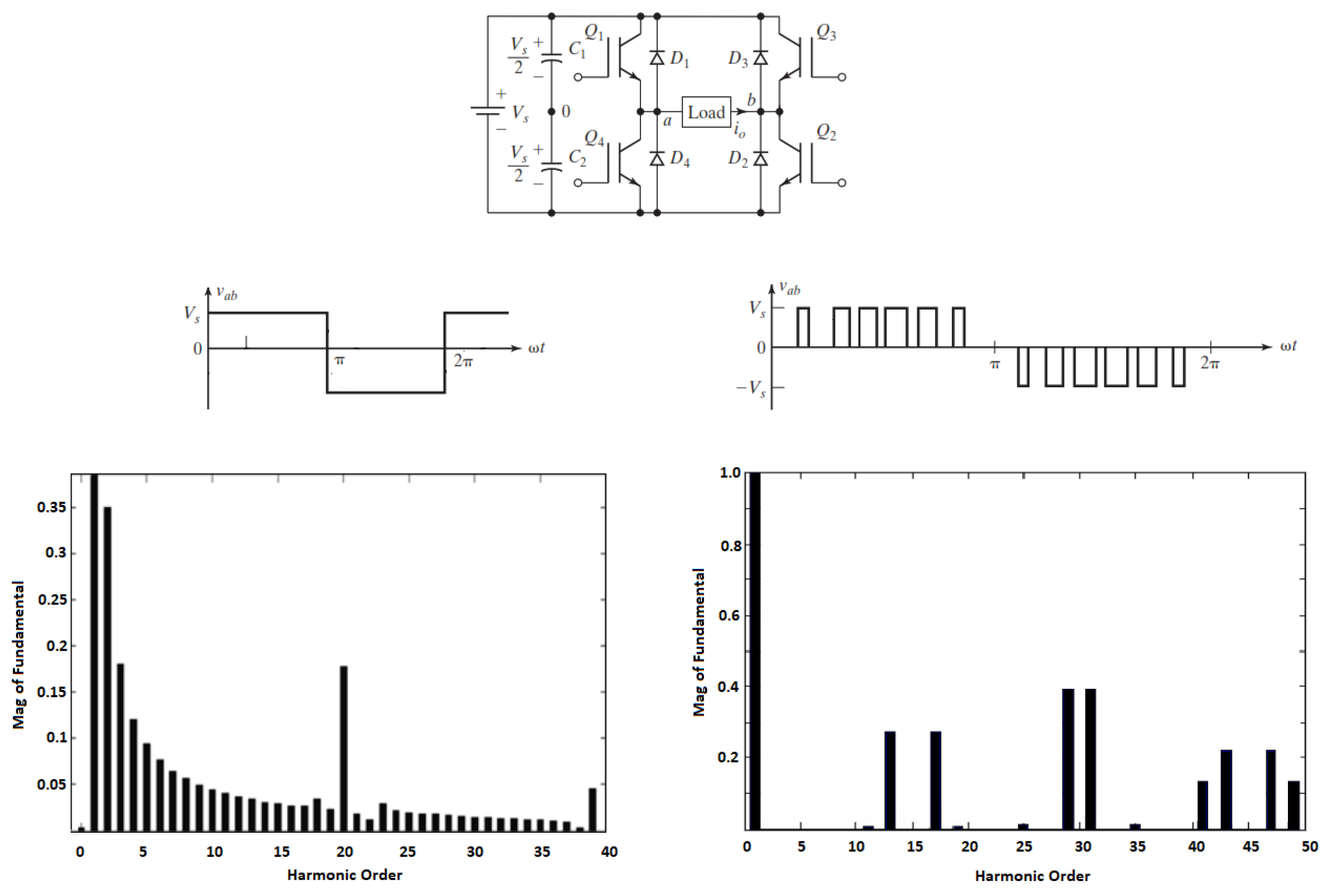
Figure 2.
Multilevel inverter conceptual topology and output waveform.
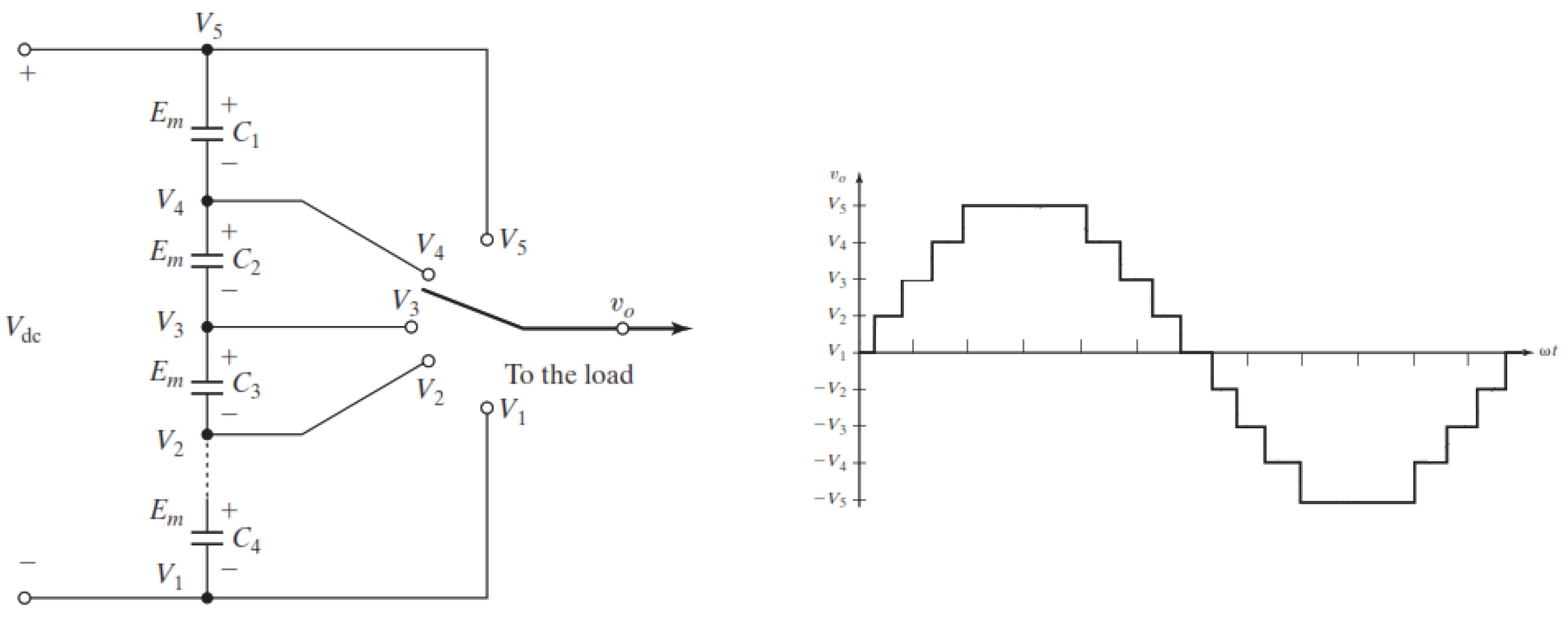
Figure 3.
Harmonic spectre in 5 and 9 level inverter.[4]
Figure 3.
Harmonic spectre in 5 and 9 level inverter.[4]
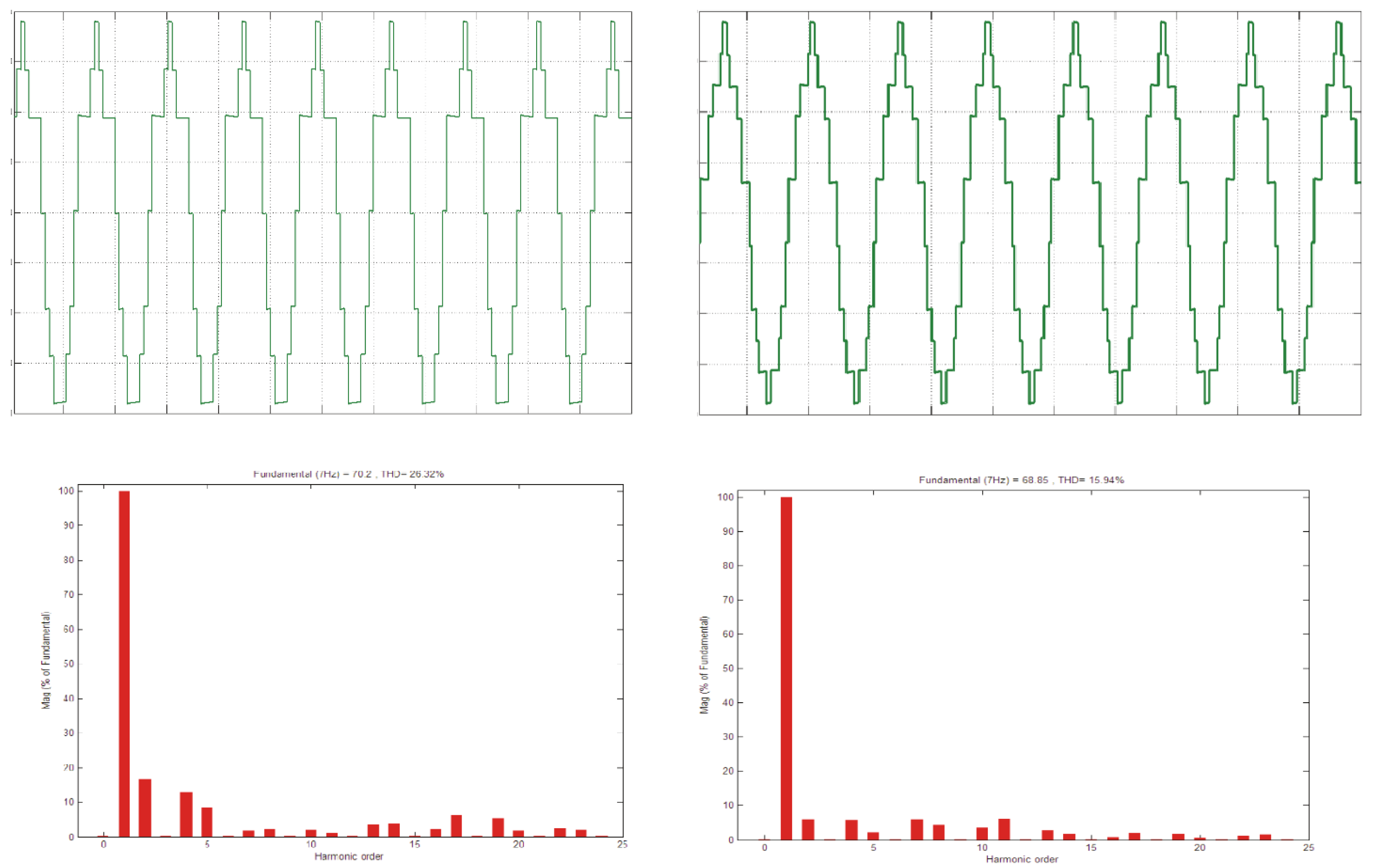
Figure 4.
Infinite level inverter schematic.
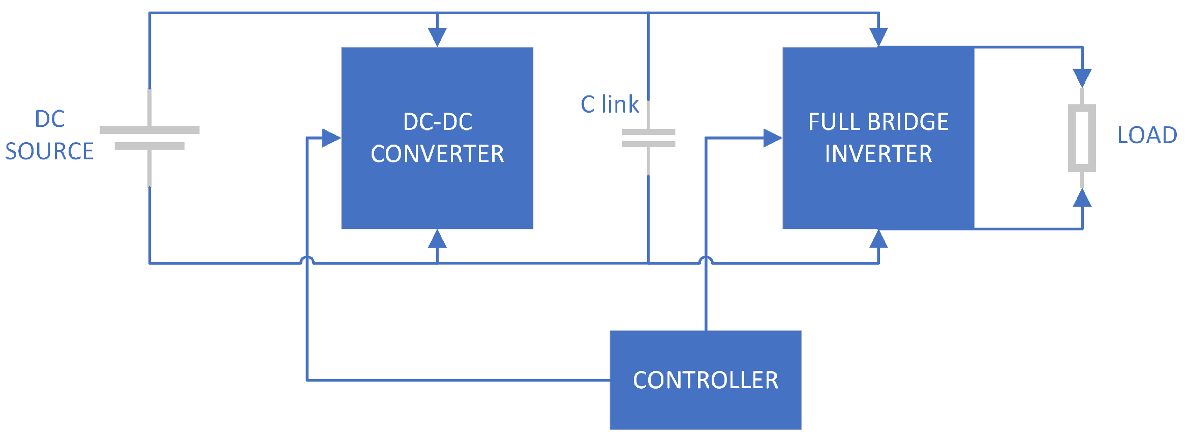
Figure 5.
BUCK converter topology.
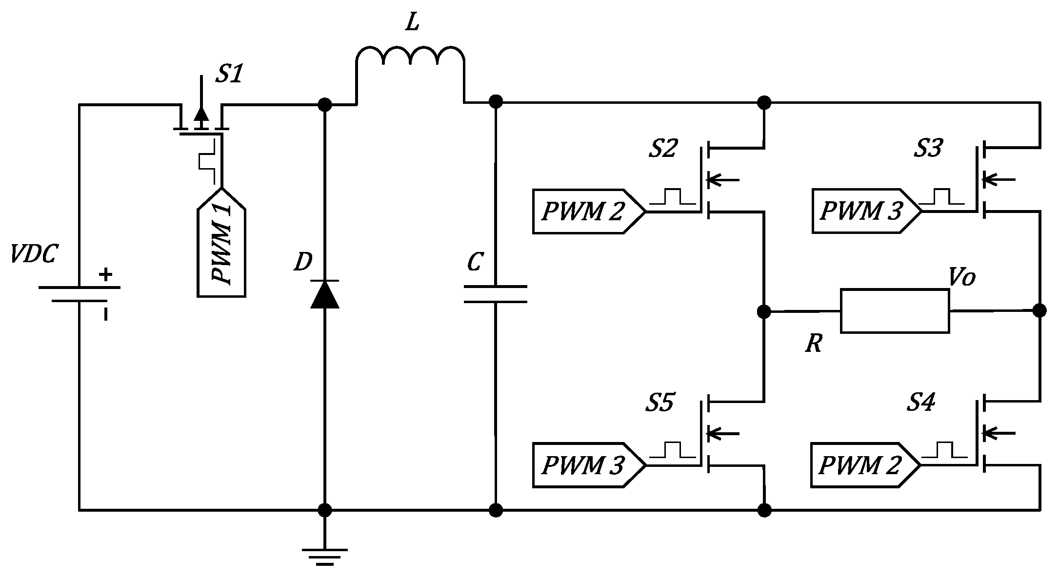
Figure 6.
BUCK converter topology.
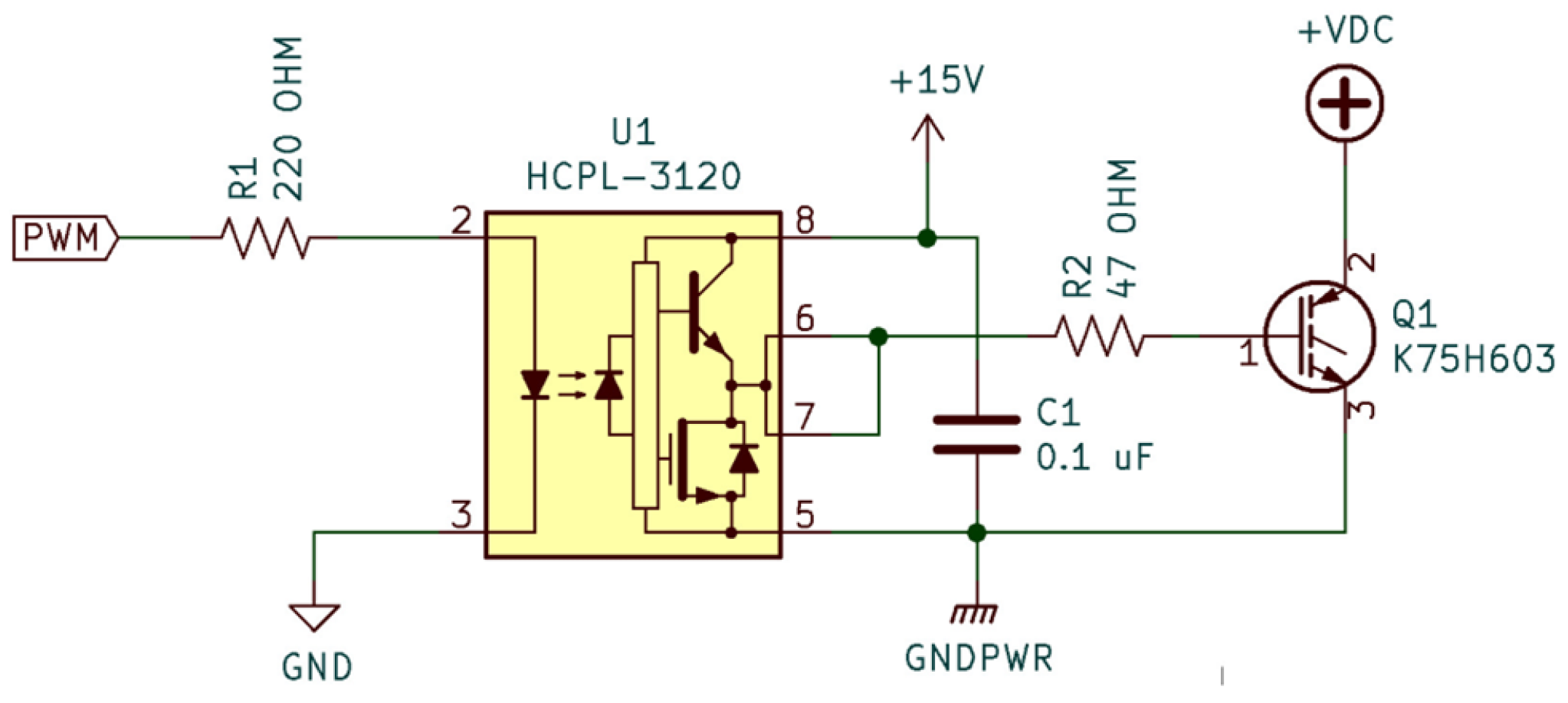
Figure 7.
Controller schematic
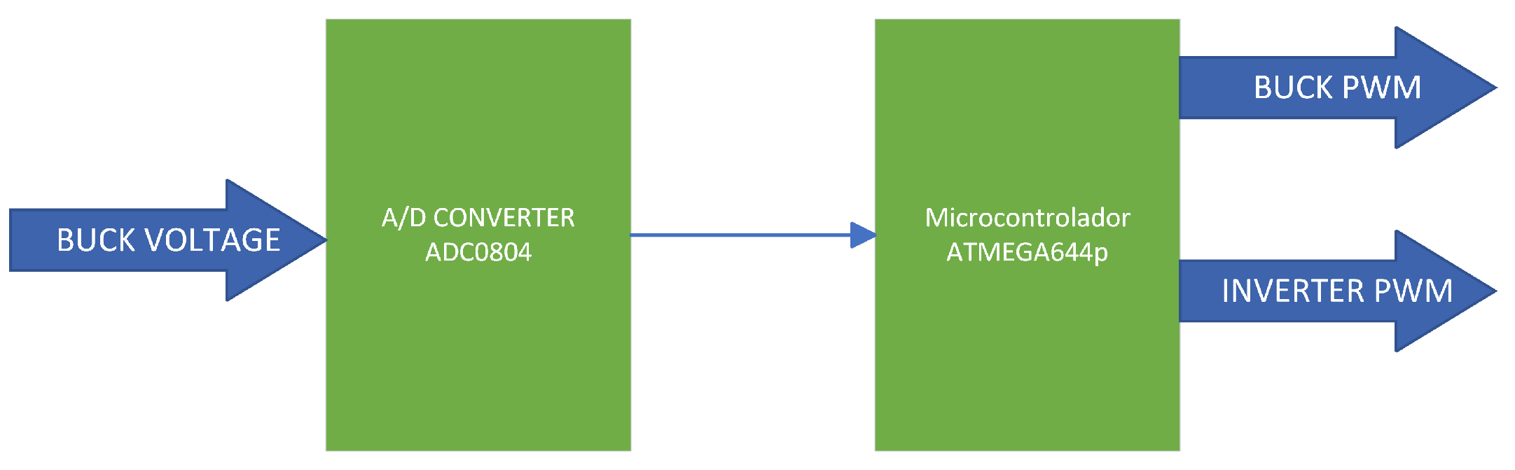
Figure 8.
ATMEGA644 program flow chart
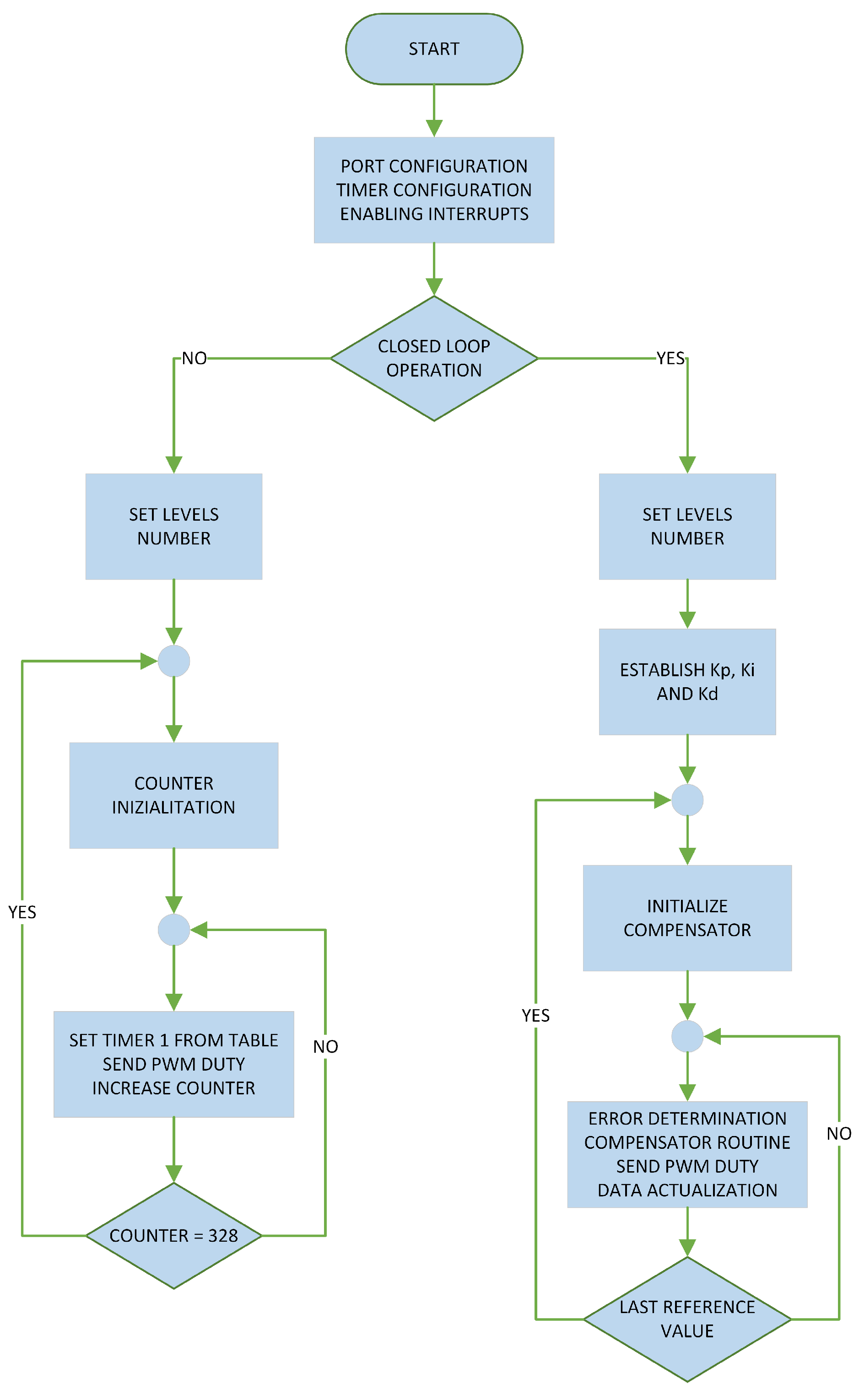
Figure 9.
Controller scheme
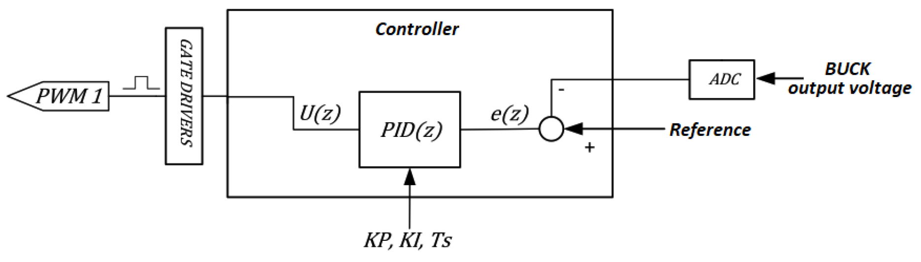
Figure 10.
Experimental hardware
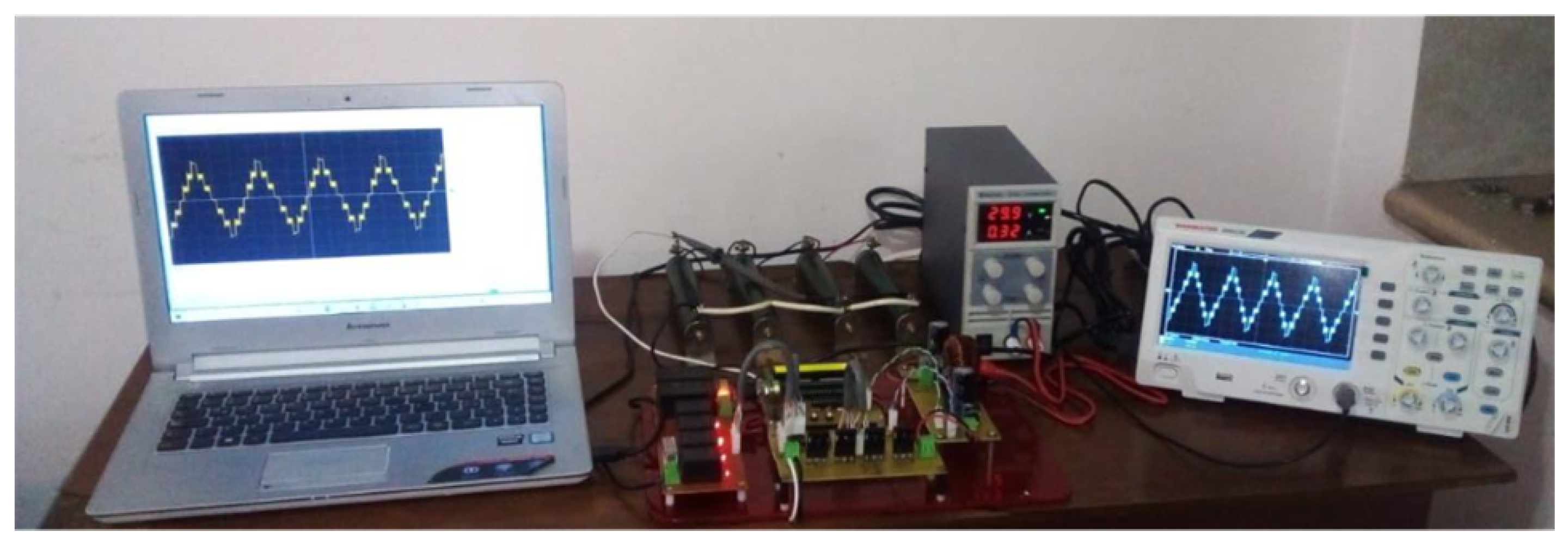
Figure 11.
Capacitance effect on Voltage output waveform
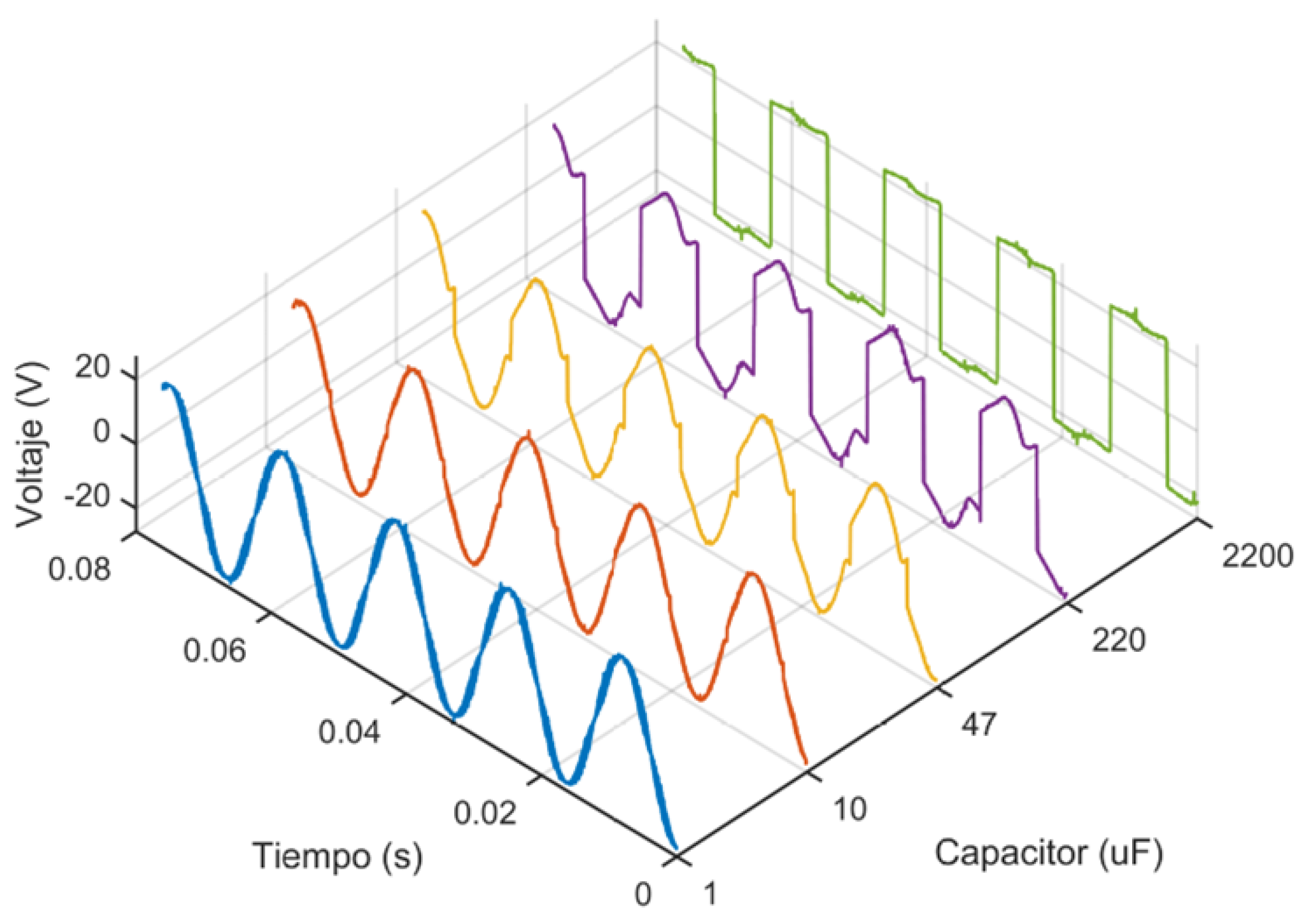
Figure 12.
Inverter output voltage waveform for 3, 5, 7, 9 and infinite level
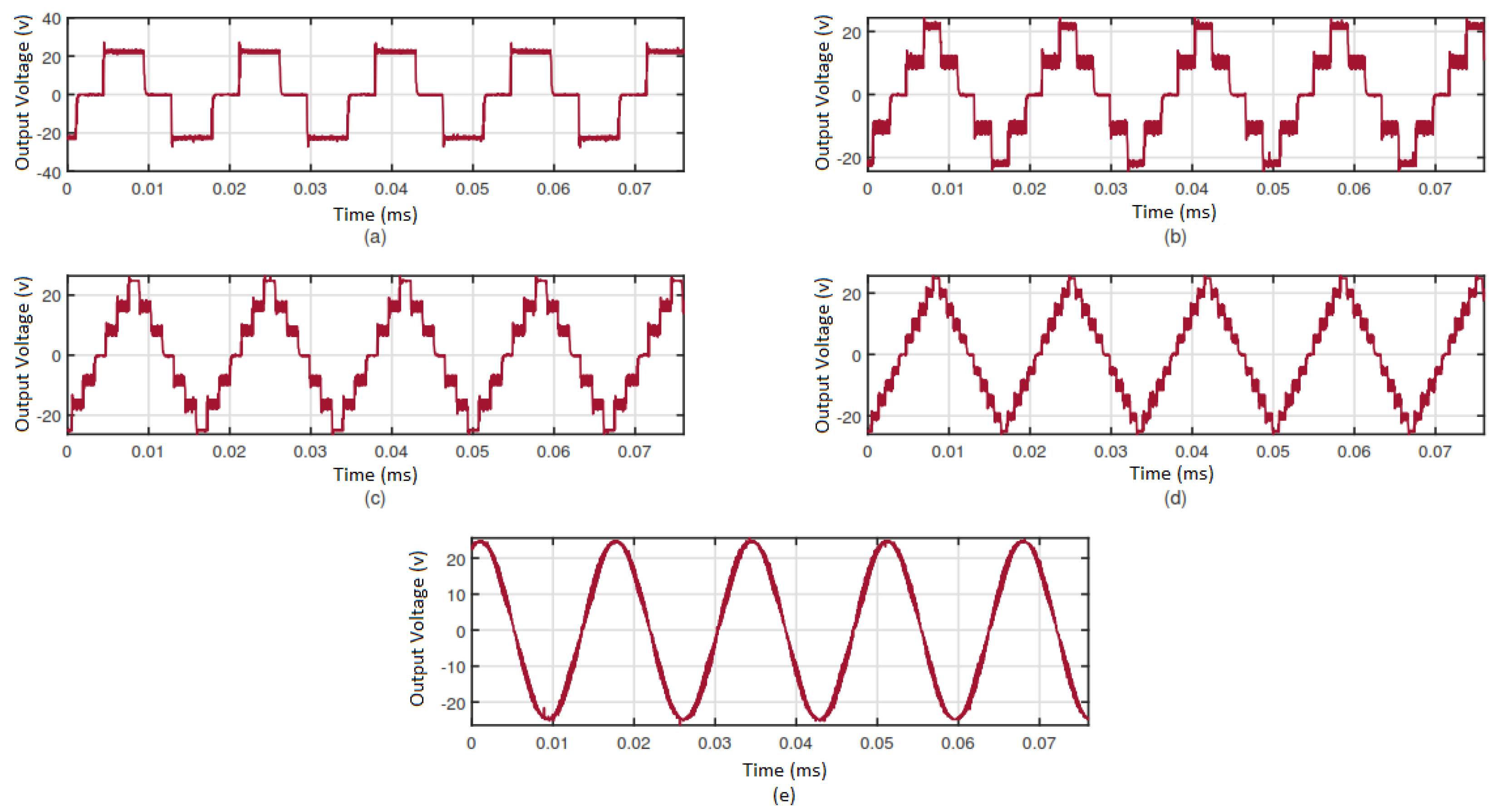
Figure 13.
BUCK converter in closed lopp operation
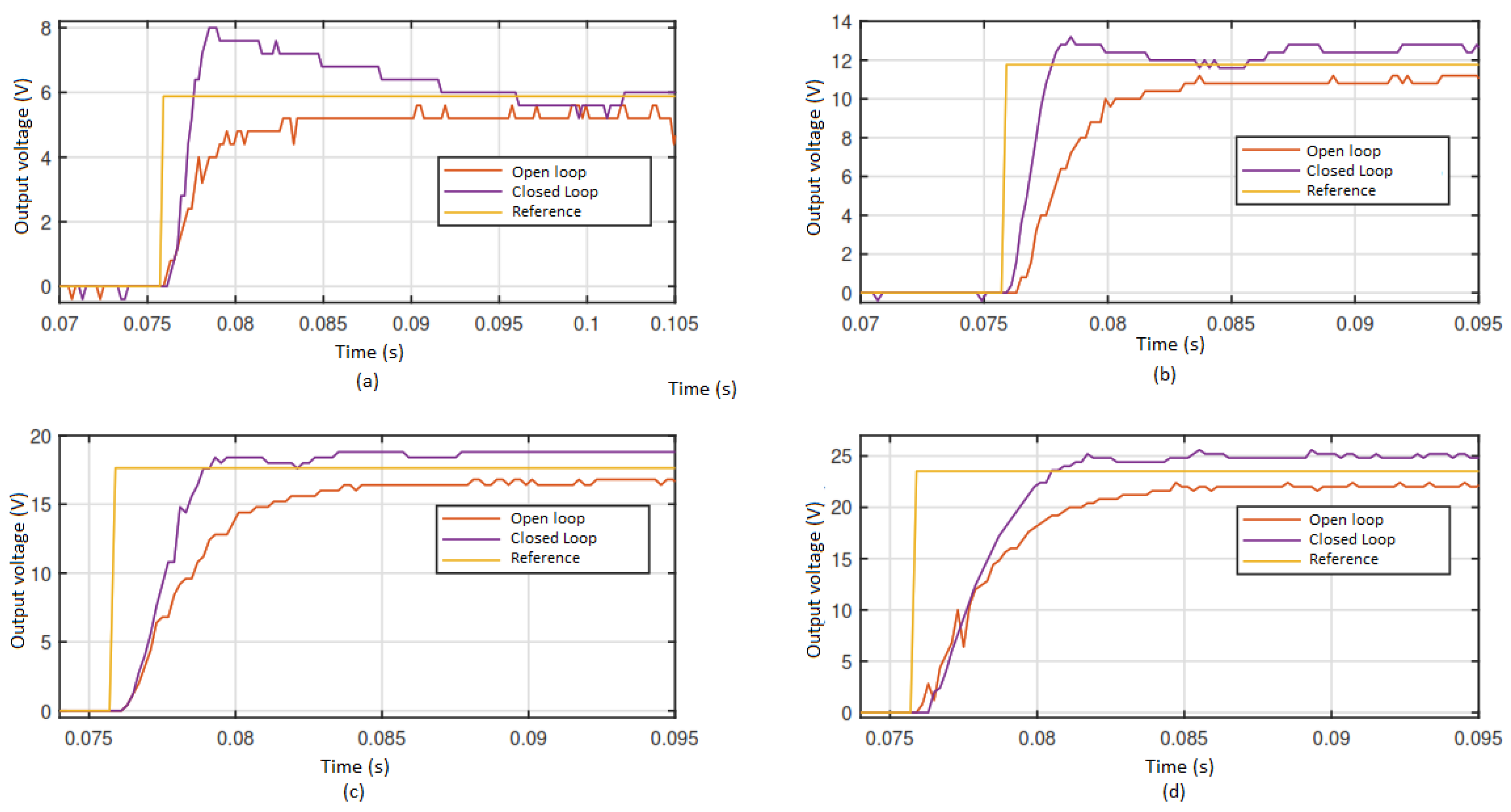
Figure 14.
Results in an infinite level inverter in closed loop operation for 3, 5, 7 and ∞ levels
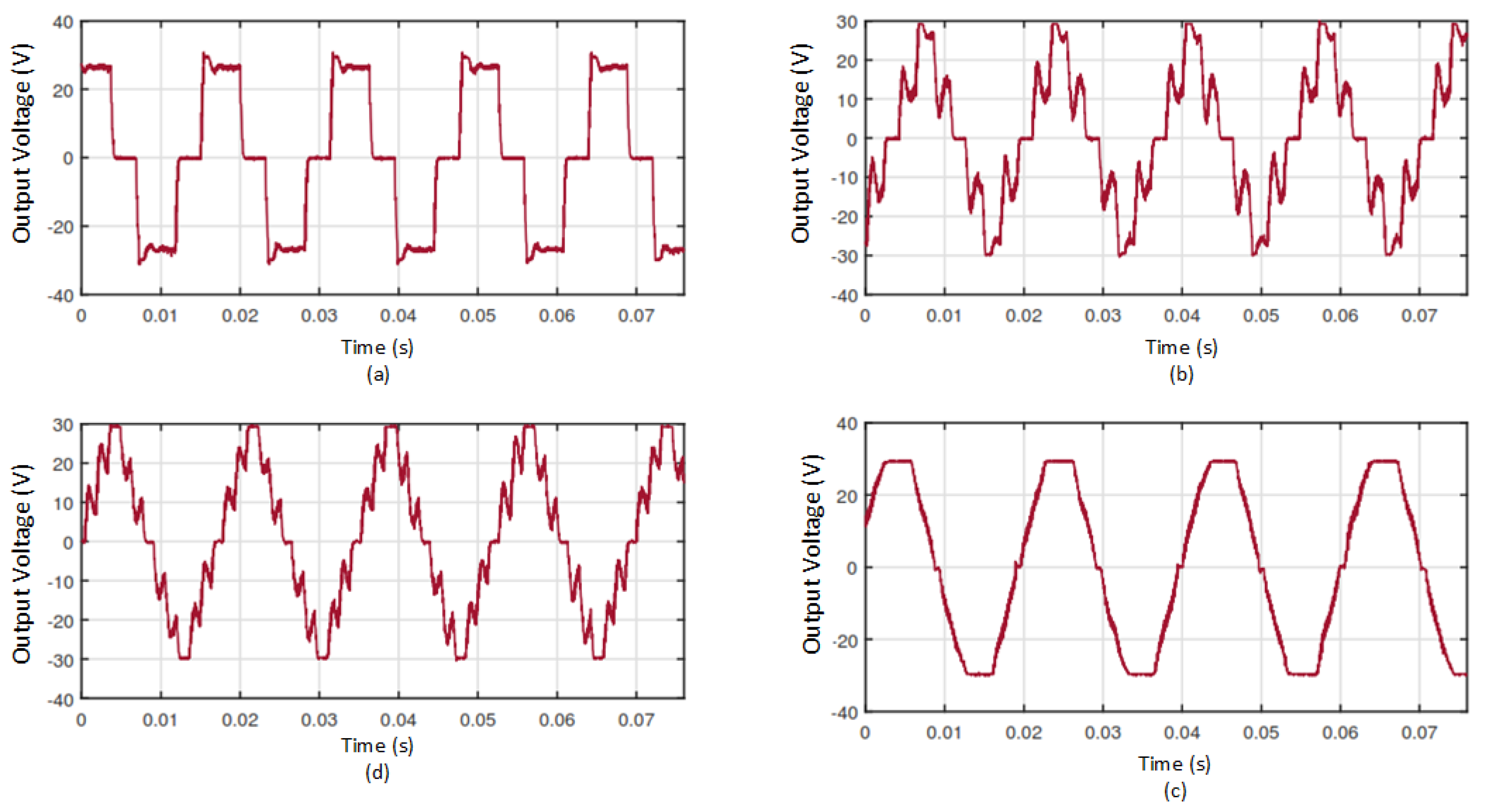
Figure 15.
Results in an infinite level inverter in closed loop operation for 3, 5, 7 and ∞ levels with
Figure 15.
Results in an infinite level inverter in closed loop operation for 3, 5, 7 and ∞ levels with
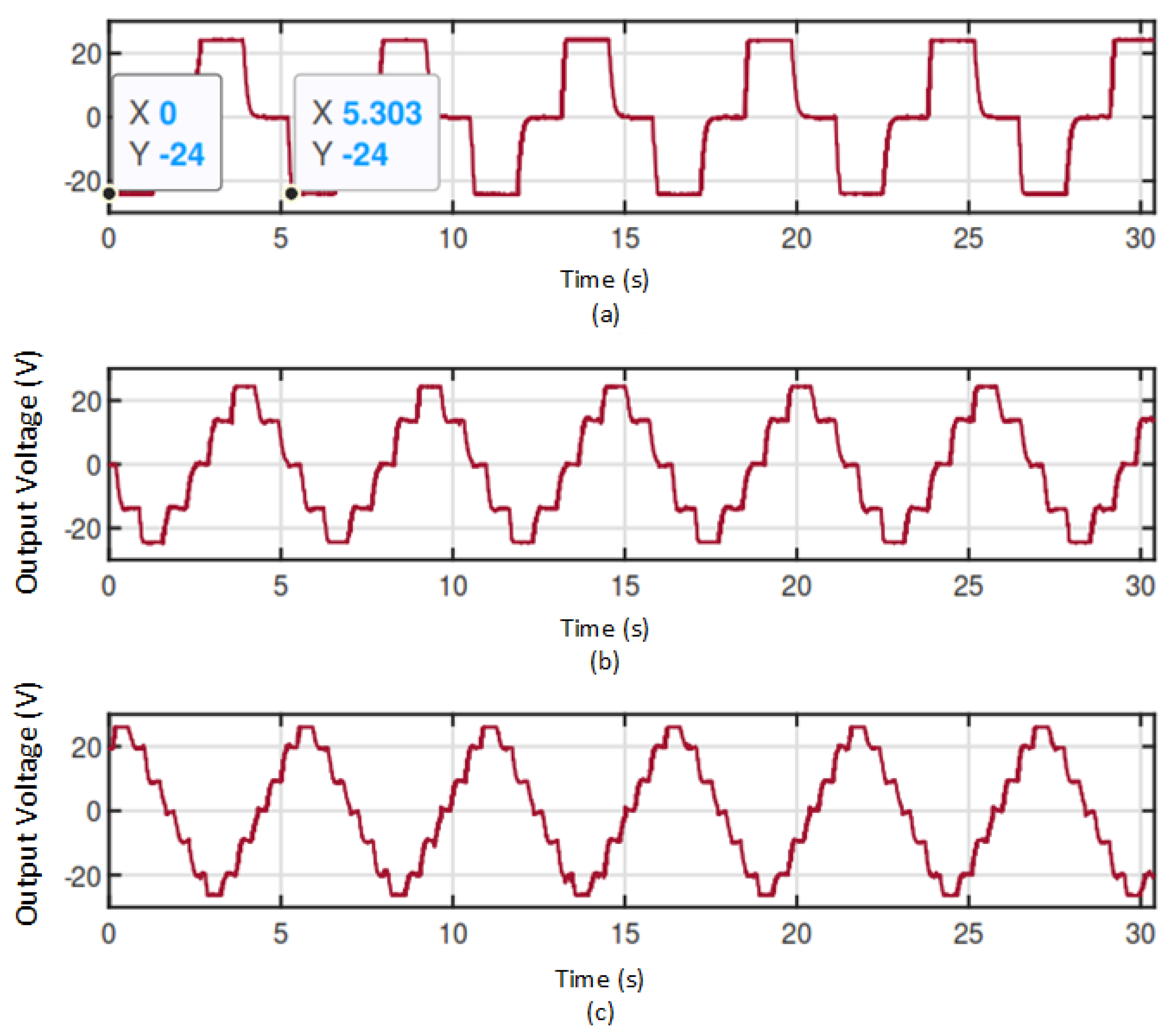

Table 1.
Electric components number in m-multilevel inverter topologies [6].
Table 1.
Electric components number in m-multilevel inverter topologies [6].
| Topology | Number of Switches | Number of Diodes | Number of Capacitors |
|---|---|---|---|
| Clamping Diode | |||
| Floating Capacitor | 0 | ||
| Cascaded inverters | 0 |
Table 2.
BUCK converter design conditions.
| Parameter | Symbol | Value |
|---|---|---|
| Input Voltage | ||
| Duty ratio | ||
| Output voltage ripple | ||
| Inductor current ripple | ||
| Switching frequency |
Table 3.
Characteristics and percentage of harmonic content of voltage signals.
| 3 Levels | 5 Levels | 7 Levels | 9 Levels | ∞ Levels | |
|---|---|---|---|---|---|
| THD(%) | 34.28 | 28.63 | 20.93 | 15.70 | 3.47 |
| Fund. (Vrms) | 16.42 | 12.68 | 14.24 | 14.21 | 17.35 |
| DC (V) | 0.05 | 0.16 | 0.13 | 0.14 | 0.08 |
| Fundamental(%) | 100 | 100 | 100 | 100 | 100 |
| h2(%) | 0.32 | 0.64 | 0.46 | 0.51 | 0.39 |
| h3(%) | 12.32 | 14.04 | 11.78 | 11.30 | 1.26 |
| h4(%) | 11.11 | 1.18 | 0.79 | 0.80 | 0.16 |
| h5(%) | 24.08 | 10.72 | 6.19 | 4.28 | 0.16 |
| h6(%) | 0.90 | 0.20 | 0.23 | 0.08 | 0.32 |
| h7(%) | 5.46 | 12.91 | 3.88 | 2.31 | 0.59 |
| h8(%) | 0.56 | 1.56 | 0.52 | 0.25 | 0.08 |
| h9(%) | 10.18 | 10.78 | 4.62 | 1.24 | 0.36 |
| h10(%) | 1.23 | 0.04 | 0.05 | 0.06 | 0.17 |
| h11(%) | 8.23 | 2.84 | 8.77 | 1.02 | 0.26 |
| h12(%) | 0.42 | 0.54 | 1.33 | 0.27 | 0.17 |
| h13(%) | 2.36 | 4.31 | 6.27 | 0.72 | 0.24 |
| h14(%) | 1.08 | 0.29 | 0.12 | 0.13 | 0.05 |
| h15(%) | 6.66 | 4.81 | 1.80 | 1.58 | 0.26 |
Table 4.
BUCK converter in open and closed loop comparison
| Closed loop | Open loop | |||||
|---|---|---|---|---|---|---|
| Voltage Reference () | (%) | |||||
| 5.880 | 1 | 28.9 | 36.05 | 3.2 | 9.21 | − |
| 11.76 | 1.2 | 19.1 | 12.24 | 4.4 | 9.01 | − |
| 17.64 | 2 | 9.61 | − | 5.2 | 8.41 | − |
| 23.52 | 3 | 6.41 | − | 4.8 | 9.61 | − |
Table 5.
Harmonic content for infinite level inverter in closed loop operation
| 3 Levels | 5 Levels | 7 Levels | ∞ Levels | |
|---|---|---|---|---|
| THD(%) | 33.51 | 34.54 | 32.77 | 58.04 |
| Fund. (Vrms) | 19.83 | 15.55 | 17.01 | 6.246 |
| DC (V) | 0.469 | 0.285 | 0.328 | 1.907 |
| Fundamental(%) | 100 | 100 | 100 | 100 |
| h2(%) | 1.58 | 0.44 | 5.90 | 11.76 |
| h3(%) | 6.89 | 14.08 | 7.72 | 4.73 |
| h4(%) | 2.57 | 1.05 | 1.71 | 8.83 |
| h5(%) | 17.85 | 15.70 | 0.75 | 4.27 |
| h6(%) | 2.61 | 0.47 | 0.79 | 2.29 |
| h7(%) | 4.83 | 12.67 | 1.57 | 2.21 |
| h8(%) | 0.36 | 3.43 | 1.62 | 2.25 |
| h9(%) | 2.54 | 12.21 | 1.31 | 4.23 |
| h10(%) | 0.78 | 0.45 | 0.43 | 3.21 |
| h11(%) | 0.38 | 3.51 | 1.85 | 1.73 |
| h12(%) | 0.13 | 1.38 | 1.67 | 1.61 |
| h13(%) | 0.11 | 1.72 | 1.38 | 1.54 |
| h14(%) | 0.43 | 0.56 | 0.83 | 1.03 |
| h15(%) | 1.36 | 0.36 | 0.29 | 0.16 |
Disclaimer/Publisher’s Note: The statements, opinions and data contained in all publications are solely those of the individual author(s) and contributor(s) and not of MDPI and/or the editor(s). MDPI and/or the editor(s) disclaim responsibility for any injury to people or property resulting from any ideas, methods, instructions or products referred to in the content. |
© 2024 by the authors. Licensee MDPI, Basel, Switzerland. This article is an open access article distributed under the terms and conditions of the Creative Commons Attribution (CC BY) license (http://creativecommons.org/licenses/by/4.0/).
Copyright: This open access article is published under a Creative Commons CC BY 4.0 license, which permit the free download, distribution, and reuse, provided that the author and preprint are cited in any reuse.


