Submitted:
22 July 2024
Posted:
24 July 2024
You are already at the latest version
Abstract
Low dropout (LDO) regulators are widely used in portable electronic devices because they 1 occupy small chip and printed circuit board (PCB) areas. This work presents the design of a low 2 noise low dropout (LDO) linear voltage regulator using folded cascode operational amplifier and 3 source follower buffer for frequency compensation. The proposed design achieves low output noise 4 with feedback loops, which makes it possible to improve load and line regulations as well as the 5 transient response for voltage applications in comparison with the literature. The designed LDO 6 linear regulator works under the input voltage of 2.8-4.8 V and provides up to 100 mA load current 7 for an output voltage of 2.6 V. 8 9 Moreover, the operational amplifier design contributes to the major reduction in the frequency 10 noise, and make sure the stability of LDO under different conditions. Furthermore, the novel LDO 11 design topology has very less dropout voltage, fast transient response and minimized power dissi- 12 pation under maximum load current, worst process corner, and maximum temperature to achieve 13 high power efficiency, maintain output voltage in the presence of fast load changes, and to lower the 14 power loss across the pass element especially at high load. Design criteria are addressed in detail. 15 16 This LDO topology is able to achieve ultra-low noise i.e. 2 /muv/√Hz for frequency >1kHz. The 17 proposed LDO is implemented in the cadence virtuoso H9A with CMOS 130 μm technology.
Keywords:
Low Dropout Regulator (LDO)
; folded cascode op-amp
; low-noise
1. Introduction
Supplying and conditioning power are the most fundamental functions of an electrical system. In modern electronics, it is very important to adapt the voltage and current levels coming from an external source to a user with different voltage-current characteristics. As the use of battery-powered portable devices such as mobile phones, laptops, and various handheld devices has rapidly increased, power management should be one of the most important issues for maximizing the battery lifetime and providing energy to multiple on-chip blocks [1]. Most electronic systems need a stable voltage to obtain performance in different operating conditions, especially in medical, military, and space fields. Sources like transformers, generators, batteries, and other offline supplies incur substantial voltage and current variations across time and they are normally noisy and jittery not only because of their inherent nature but also because high-power switching circuits like central-processing units (CPUs) and digital signal processing (DSP) circuits usually load it. These rapidly changing loads cause transient excursions in the supposedly noise-free supply, the results of which are undesired voltage drops and frequency spurs where only a DC component should exist.
A voltage regulator is an integral part of the power management system (PMS) of all electronic devices and it has been the focal point of research over the past few years [2]. The role of the voltage regulator is to convert these unpredictable and noisy supplies to stable, constant, accurate, and load-independent voltages, attenuating these ill-fated fluctuations to lower and more acceptable levels. A simple and cheap solution to regulate an output voltage powered by a higher input consists of using Low-dropout (LDO) regulators. An LDO creates a drop voltage by a series element between the input and the output. Due to their inherent simplicity, LDO is ideal off-chip and on-chip solutions for powering noise-sensitive loads, such as phase-locked loops, analog-to-digital converters, and sensor interfaces, because they convert voltage through a linear operation with no output voltage ripples [3]. An LDO requires no bulky components such as inductors, and therefore multiple of them can be integrated on a chip. Furthermore, since an LDO can create an independent voltage domain, each core/block of an SoC can operate at the optimal voltage, maximizing performance and energy efficiency [4]. The primary role of an LDO is to provide a regulated voltage by filtering the residual ripples from the switching converters. with low ripple to the individual functional blocks in an SoC [5]. The main issues concerning the LDO design consist of noise minimization and robustness against parameters’ variations.
Typical LDO uses a resistive divider to set the output voltage, so the noise gain is equal to the AC closed-loop gain, which as it turns out, is the same as the DC closed-loop gain [6]. LDO voltage regulators result in small voltage drops across the power transistor and provide a well-regulated low-noise voltage [7]. There are many sources of intrinsic noise in LDO. The major types of intrinsic noise include the following: thermal noise, 1/f noise, shot noise, and burst, or popcorn, noise [8]. To suppress thermal and flicker noise, conventional LDOs utilize highly filtered voltage references at their inputs and bypass capacitors at their outputs. However, with technology scaling, noise increases significantly. Since the corner frequency is a weak function of most transistor parameters, suppression of low-frequency noise from supply regulators in sub-micron CMOS processes is becoming a critical design [9].
The purpose of this work is the design a Low Drop Regulator (LDO) with low noise specifications to provide its final user with a stable voltage independent within certain limits of the voltage, process variations of its components, and the temperature. The LDO is designed in such a way as to have a low dropout voltage, low noise, high efficiency, good transient response, and stability over a wide range of frequencies. An optimal way of folded cascode op-amp is designed to ensure high gain, single pole, good noise performance, and large output swing as compared to other architectures of operational amplifiers since op-amp is one of the major sources of noise in LDO. Moreover, the noise performance is further reduced from the point of view of the process, by the implantation of a layer of fluorine on the poly-silicon which reduces the 1/f noise by 30%.
After a brief introduction of the fundamentals of these devices, all the phases of the design at the transistor level will be described to obtain low noise performances in all supply voltage ranges, processes, mismatches, and temperature conditions. LDO regulators find extensive use in system-on-chip (SoC) solutions where there are incorporate numerous functions, many of which switch simultaneously with the clock, demanding both high-power and fast response times in short consecutive bursts. The bandwidth performance of such a regulator guarantees the ability to respond quickly to these transient variations of the above circuits. Regulators also protect and filter integrated circuits (ICs) from exposure to voltages exceeding junction-breakdown levels.
The work is organized as follows. In section II, the LDO fundamentals and literature review are presented. In section III, the simulation of LDO with ideal components except for the pass element, the size of the pass element is designed in such a way to provide regulation in all operating conditions. In section IV, the design of the folded cascode operational amplifier and its frequency compensation is presented with a source follower buffer. The op-amp designed provide huge noise reduction. In section V, the test results are presented with different input voltage and load conditions, and in section VI conclusions are presented. The novel topology of LDO ensures low dropout voltage, fast transient response and minimized power dissipation to achieve high power efficiency, maintain output voltage in the presence of fast load changes, and to lower the power loss across the pass element especially at high load.
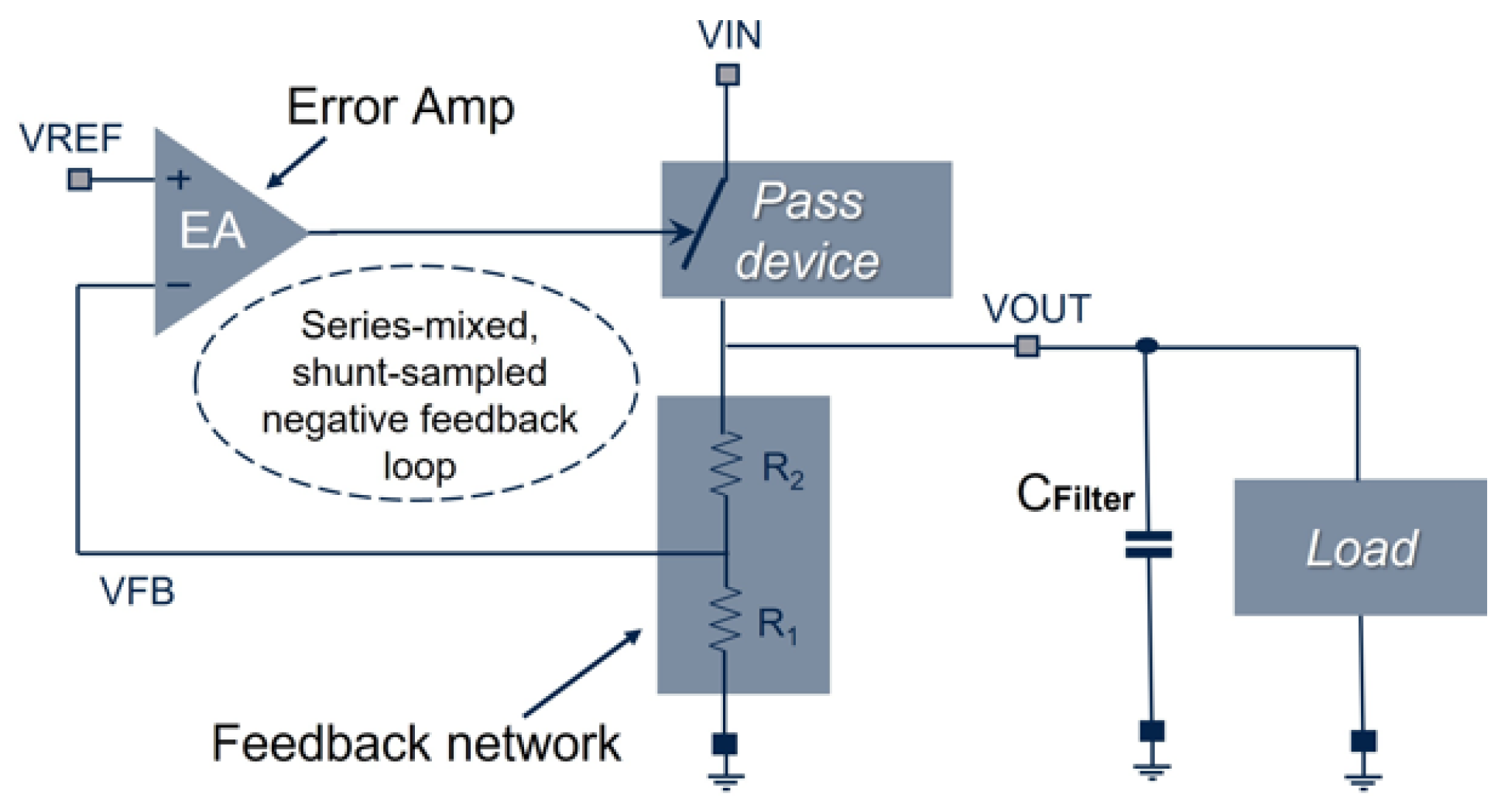
Figure 1.
Basic structure of an LDO.
2. LDO Fundamentals
A low dropout regulator is a device able to regulate output voltage with changing input voltage. It is a DC-DC linear converter that stabilizes the output voltage with a small difference in input voltage, this input-output voltage difference is called dropout voltage and is used to measure the efficiency of LDO. A typical architecture of LDO contains four basic elements which are voltage reference, error amplifier, voltage divider, and a series pass element. The error amplifier amplifies the difference between the reference voltage and feedback voltage obtained by the potential divider. The series pass element is controlled by the error amplifier which in turn controls the output current. The negative feedback loop shunt-samples the output voltage to ensure load-current variations have little impact on and series-mixes a sensed version of (via feedback voltage ) with dc input reference voltage to establish a virtual short between and , directly relating and regulating to . Finite loop gains, however, limit the efficacy of this regulating short, giving rise to nonzero load- (LDR) and line-regulation (LNR) effects on the output, that is, small variations in when confronted with changes in load current and input line voltage [10]. The output voltage can be given in terms of output resistors and reference voltage [11]:
The behavior of an LDO can be described by different parameters which are divided as [10]:
- Dropout Voltage
- Quiescent current
- Line regulation
- Load regulation
- Junction temperature
- Load transient
- Line transient
- Noise
- PSRR
- Stability
2.1. Stability Analysis
Since LDO is a negative feedback loop its phase margin should be positive. The LDO with compensation is shown in Figure 2. The stability of the LDO depends on the poles and zero location. The error amplifier, output capacitor, and pass element are responsible for the position of poles. To make the LDO stable over the required range of input voltage it is necessary to design each element carefully. The output voltage of an LDO depends on the load current and also on equivalent series resistance ESR and output capacitance . The output voltage variations can be given as:
where is the output voltage oscillations is the voltage affected when ESR is added is the response time of LDO By equation 2, we can see that output voltage oscillations are inversely proportional to the output capacitance.
For the error amplifier, a folded cascode structure is selected with a common source buffer to lower the output impedance of the error amplifier [12]. The structure of the error amplifier can be seen in Figure 3.
As discussed the stability of LDO is determined by the position of poles, the dominant pole of LDO is due to the output capacitor. To find the poles we can first find out the output impedance. The first pole (p1) is due to the PMOS pass transistor output resistance plus the equivalent series resistance ESR and the output capacitance . Looking at Figure 2 we get
where is the output resistance of pass element, is the output capacitor, and are the resistances of the voltage divider.
Since the resistances of the voltage divider and are greater than and the capacitive impedance, we get
The first pole can be found at
The second pole, due to the output impedance of the op-amp and parasitic capacitance of the large pass element, is at:
where is the output impedance of the error amplifier and is the parasitic input capacitance of pass transistor.
The zero is at
2.2. Noise
Noise occurs in transistors and resistors and is considered a physical phenomenon. Mainly, transistors consist of flicker and shot noise. Thermal noise is generated by the resistive elements in a MOSFET. Thermal and shot noise are random noises and do not depend on frequency. Another type of noise that is present in MOSFETs is flicker noise which is caused by charges present at the gate of MOSFET. Unlike thermal and shot noise, flicker noise is frequency dependent, and it decreases as frequency increases but at low frequencies, it has a great impact on MOSFET performance. At the lower frequency, the influence of intrinsic noise is more as compared to higher frequencies [13].
2.3. Noise Sources in LDO
- Voltage reference
- Error amplifier
- Series pass element
- Resistor divider
The major contribution of intrinsic noise in LDOs is from voltage reference and error amplifier. The noise can be estimated by the following equation
The two major sources of noise in an LDO are the error amplifier and the voltage reference due to the presence of large circuitry with many passive elements
3. Design and Simulation
To start, the targeted DC output voltage prescribes the gain ratio required from output feedback resistors and concerning , given the series-mixed feedback loop approximately equates to . DC conditions like input voltage , load or output current , and dropout voltage then set the basic operating requirements of the series pass device. In this chapter, each block of LDO is designed and simulated separately using cadence virtuoso H9A with technology .
3.1. Choice of MOSFET
We have chosen PMOS as the Pass Element because the output voltage is higher in this particular scenario since NMOS is positive signal driven concerning output, while PMOS is negative signal driven concerning input so we may need a charge pump to operate the NMOS at lower voltages. Secondly, when we use a charge pump with NMOS it may cause some oscillations at the output which is not desirable for the low-noise LDO. Thirdly, the input voltage in our case is higher as in PMOS the (where is the output voltage, is the drain-source saturation voltage and is the gate-source voltage) but using the NMOS we have which is not desirable with high because the output voltage will not be regulated. The PMOS operates in saturation region for most of the output load following the below equations
The choice of pass element also depends on the area requirements we want to achieve. PMOS as a pass element requires increases in the area of silicon 3x times as compared to NMOS. So the choice is a trade-off between all the requirements we want to achieve. Keeping in my mind all the parameters, the width over length (W/L) ratio is designed as described in Table 1.
3.2. Feedback Network
The feedback network is comprised of a potential divider by which the voltage is fed back to the non-inverting terminal of the op-amp. The values of and are selected to provide minimum quiescent current i.e. the minimum current required to power the LDO when the load current is zero while also taking into consideration the size of the resistor. The resistor ladder can be designed by considering the following equation
In terms of the quiescent current , the values of and can be retrieved as
It is preferable to have a low quiescent current value in LDO but it will lead to very large values of resistors resulting in large size which is not preferable. Hence, the choice of resistor ladder is a trade-off between power consumption and area size. In our scenario with a reference voltage is 1.2V and the desired output voltage is 2.6V the resistor values of 167.67k and 100k are designed to keep the feedback network and output voltage regulated.
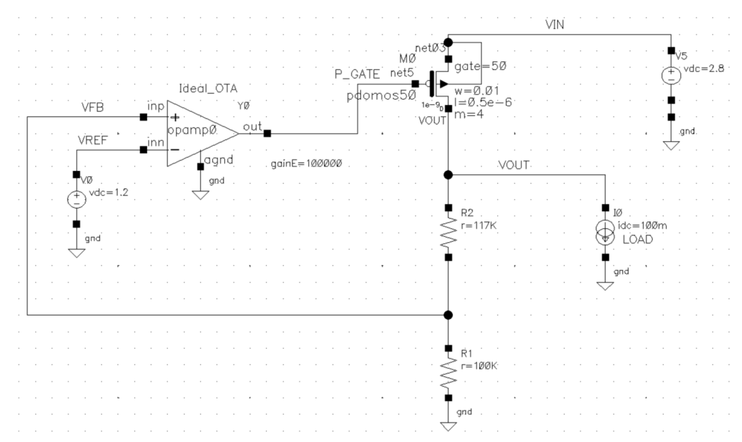
Figure 5.
Simplified constant loop with ideal components except for Pass element.
4. Design of the Operational Amplifier
The design of the operational amplifier is the most important part of the LDO in which the output voltage is fed back to keep the regulation with changing load currents. The difference between the reference and feedback voltage is amplified which in turn drives the gate of the pass element, any error in the voltage is compensated by the pass element. The architecture of op-amp is selected keeping in mind the noise, stability, and offset. The folded cascoded architecture is selected because of its increased stability at no-load conditions. A folded cascode op amp has a very high gain, single pole, good noise performance, and large output swing as compared to other architectures of operational amplifiers. It is also very suitable for negative feedback networks because of its very large small signal gain. The following equations could be considered for the design of an operational amplifier [15].
4.1. Architecture
The selected architecture of the op-amp is shown in Fig 6. The two parameters and represent PMOS differential pair with identical transistors, hence the current i.e. 2uA. In Figure 6, the blue area shows the input differential pair, the yellow area the different current mirrors while green area the cascode topology of the amplifier. The main reason for using this architecture is the small size and simplicity of the circuit which gives high gain. Folding the positive polarity transistors in folded topology decreases the headroom for the circuit giving the same performance even at low supply voltage. Since the current mirror’s output resistance appears in parallel with the output resistance of the amplifying portion of the circuit, the current source must be cascoded as well, so as not to extinguish all of the benefits that were gained by the cascode in the first place [12,16].
The first step of the design is to decide the amount of current to use based on the power dissipation. A way to select the current is that the current through the differential input pair should be larger than the output current stage to help ensure maximized gain and low power dissipation, and can be as large as four times. To determine the W/L ratio of each of the transistors, either the gain requirements or the input and output range requirements can be used. Each of these requirements is dependent upon the transconductance () and overdrive voltage (). By selecting the desired or , and using equations 18 and 19 below with the previously calculated currents, the appropriate W/L ratios can be retrieved.
If after calculating the W/L ratios for both the input and output range, the gain and phase margin requirements are not met, there are some modifications that the designer can make. To increase the gain of the circuit, the size of the input differential pair transistors can be increased. This will increase the gain of the circuit but also decrease the phase margin of the circuit. To increase the phase margin of the circuit, a compensation capacitor can be placed at the output node of the amplifier. The increased capacitance will improve the phase margin, however, this will trade away some of the bandwidth. Two pairs of resistor and capacitance are added at the input differential pair and at the output of op-amp that will generate a zero at
Table 2 shows the W/L selected for each MOSFET.
4.2. Stability
After selecting the size of the op-amp, frequency domain analysis is done to ensure the stability of the op-amp in all load conditions. At first, the allocation of poles and their contribution in the phase and gain margin were found. The behavior of the op-amp can be given by the following equations [17]:
While designing the op-amp following considerations concerning W/L ratio, Bias current, poles allocations, and differential pairs should be taken into account [17]:
-
W/LAll the MOSFET should work in the saturation region and the aspect ratio must be designed in such a way as to prevent their operation in the sub-threshold region [18].
- Bias Current The current mirrors and current source act as active loads in the op-amp so care must be taken to decide the bias current. When the bias current is increased the voltage at and will increase, but should not leave the saturation region. Alternatively when the bias current decreases the voltage at and will decrease which may leave in the sub-threshold region.
-
Poles AllocationThe dominant pole of the op-amp is due to the output capacitor used for compensation. The non-dominant pole of the op-amp is due to the NMOS cascode branch, located at a very high frequency which does not contribute to the stability.
- Differential Pair Differential pair is limited to the offset, which depends on the Load current, and flicker noise. The drain-source resistance of the differential pair must be kept high to make the non-dominant pole at a very high frequency.
4.3. Noise
The op-amp designed above is simulated to achieve the required noise level i.e., 2V/Hz at f < 1kHz. At low frequencies, the noise spectrum of an LDO is dominated by flicker noise. The main reason for using folded-cascode architecture is the small size, simplicity of the circuit, and low noise parameters. The W/L of the differential pair of the op-amp is chosen to maximize the gain and minimize the input-referred noise of the op-amp. The contribution of flicker noise is also reduced by altering the aspect ratio of the cascode topology.[12] The flicker noise in the op-amp is proportional to the bias current, reducing the bias current reduces the flicker noise, hence the bias current was optimized to achieve low noise with high gain and bandwidth.
4.4. Buffer
To stabilize the LDO a source follower buffer was designed with op-amp to provide low output impedance to the pass element [19] in that way the pole of the pass element is shifted to higher frequencies and does not contribute to the stability. [1] The output aspect ratio is 4 times the input aspect ratio, so the output impedance is 4 times smaller than the input impedance [20,21].
After designing each component, all are connected to simulate the LDO. The LDO is simulated under no load and full load conditions to stabilize the system in all load conditions.
4.5. Enable
An enable input is added in the LDO which when ’0’ the LDO is OFF and when ’1’ LDO operates. The Enable input (EN), available in positive and negative logic, turns the device on and off by an external signal. Active-high logic activates the device when the voltage at the EN input exceeds the high-logic threshold. The active-low logic switches the device off when the EN voltage falls below the logic-low threshold. The EN function is an important feature when sequencing power supplies in systems.
When the LDO is turned off and connected to the battery system, the input current will be limited. This Shutdown current is commonly confused with the quiescent current which is the current drawn by the device when it is enabled and operating with no load. Both shutdown and quiescent current is important parameters when realizing long battery lifetimes in portable devices. The enabling circuit is shown in Figure 7.
4.6. Pull Up and Pull Down Network
Pull-up and down networks are designed for the LDO to ensure that no current flows when the LDO is OFF. Pull-up is used to make the output logic high while pull-down is used to make the output logic low. Pull-up consists of PMOS transistors while pull-down is made with NMOS transistors. The pull-up transistor will act as a source when the output is logically high. The pull-down transistor will act as a sink when the output is logically low. During logical high output, the pull-up transistor is switched on and the lower pull-down transistor is switched off. Similarly, during logical low output, the pull-down transistor is switched on and the pull-up transistor is switched off. In both of these two outputs, the output current (source or sink) is low due to the complimentary pair of P-MOS and N-MOS transistors at the output and also at the input of any logic gate. Hence CMOS logic gates consume reduced power. The pull-down network PDN network can be seen in Figure 8.
4.7. Short Limiter Protection
A current loop is introduced in the main circuit to protect in case of
- (1)
- High current
- (2)
- Output shorted to ground
A current () is produced that is the copy of the pass element current by the following equations:
Since are same for both. Dividing both equations we get:
The current () is times smaller than pass current (). We select the size of PMOS smaller by a factor of a thousand than the pass element. The is selected to be 160mA. Hence,
To create a voltage at the drain of PMOS a resistor is introduced and is connected to the operational amplifier which compares this voltage with the reference voltage to control the current loop. The circuit connection is shown in Figure 9.
5. Results
5.1. Noise
The folded cascode architecture has good noise performance. The op-amp designed above is simulated to achieve the required noise level.
As shown in Figure 10, the noise is at 10 Hz.
The LDO is simulated at different input voltages and different load currents to make sure that it works for all conditions. First, we simulated LDO with an input voltage of 2.8V, then we increase the input voltage to 3.2, 3.8, and 4.8 to find the stability of LDO.
The obtained results are shown in the following tables:

Table 3.
Parameters at load (0 mA).
| Parameter | Vin=2.8 V | Vin=3.2 V | Vin=4.8 V |
|---|---|---|---|
| Gain (dB) | 60 | 61 | 61 |
| Phase Margin | 48 | 47 | 47 |
| Bandwidth (Hz) | 779.8 | 801 | 790 |
Table 4.
Parameters at load (10 A).
| Parameter | Vin=2.8 V | Vin=3.2 V | Vin=4.8 V |
|---|---|---|---|
| Gain (dB) | 66 | 66 | 66 |
| Phase Margin | 40 | 40 | 39 |
| Bandwidth (kHz) | 1.11 | 1.15 | 1.148 |
Table 5.
Parameters at load (100 A).
| Parameter | Vin=2.8 V | Vin=3.2 V | Vin=4.8 V |
|---|---|---|---|
| Gain (dB) | 78.674 | 78 | 80.31 |
| Phase Margin | 32 | 32 | 32 |
| Bandwidth (kHz) | 2.7 | 2.7 | 2.74 |
Table 6.
Parameters at load (10 mA).
| Parameter | Vin=2.8 V | Vin=3.2 V | Vin=4.8 V |
|---|---|---|---|
| Gain (dB) | 81.59 | 81 | 66 |
| Phase Margin | 63 | 63 | 39 |
| Bandwidth (kHz) | 50.5 | 53.45 | 54 |
Table 7.
Parameters at load (100 mA).
| Parameter | Vin=2.8 V | Vin=3.2 V | Vin=4.8 V |
|---|---|---|---|
| Gain (dB) | 59.67 | 82.13 | 94.35 |
| Phase Margin | 40 | 36 | 35 |
| Bandwidth (kHz) | 136 | 161 | 180 |
5.2. Transient Response
If an LDO’s load suddenly changes from high speed to low-speed state or vice versa, as a consequence the operating current change abruptly, resulting in a step change in LDO’s load current. An LDO should maintain its output voltage even in the presence of fast load changes. In actuality, the output voltage of an LDO does not remain constant but is changed slightly because it can not respond to instantaneous fluctuations in load currents. When a load changes, the negative feedback network of LDO causes the output back to its original steady-state value. The transient response simulations are done with different temperatures and different corners i.e., Fast-Fast Average (FFA), Fast-Slow Average (FSA), Slow-Fast (SFA), and Slow-Slow Average (SSA) as shown in Figure 12.
5.3. Dropout Voltage
Output voltage vs input voltage is plotted in Figure 13, with changing input voltage, the behavior of the pass element can be divided into three regions with respect to the input voltage which are as follows [22]:
-
Region Left to the cursor: indicates the linear region in which the pass element acts as a resistor. This region is called the dropout follower and the behavior of the output voltage can be described by the following Equation (32)where is the load currentis the ON resistance of pass element
- The knee point: At this point, the pass element is in the dropout region, which is the smallest difference between the input and output voltage, which is required to maintain regulation. The dropout voltage is given as:
- Region Right to the cursor: indicates the saturation or regulation region in which the output voltage remains constant with respect to the input voltage. In this region, the pass element acts as a current generator.
The dropout voltage regions can be seen in Figure 13.
The minimum dropout voltage shown in Figure 2 is 67 mV. The dropout voltage in regulation must be measured keeping in account the worst-case scenario i.e. with maximum load current, worst process corner, and maximum temperature. Low dropout voltage is important to achieve high power efficiency and to lower the power loss across the pass element especially at high load.
5.4. Junction Temperature
LDOs always have a temperature limitation to ensure proper working. The maximum allowable temperature should be specified to minimize power dissipation. To find the maximum allowable temperature, we must calculate allowable dissipation, PD(max), and the actual dissipation, PD, which must be less than or equal to PD(max). The maximum power dissipation limit is determined using the following Equation (34)
where is the maximum allowable junction temperature is the thermal resistance junction to ambient is the ambient temperature The power dissipation can be calculated by equation 35:
Figure 14 shows power dissipation curves concerning output current with input voltages the operating limit in which the regulator can be operated safely. It’s important to use thermal protection for LDO, which will turn off the device whenever the safe limit is exceeded.
5.5. PM and GM at Different Iout and Vin
After stabilizing the LDO with different load currents and input voltages Phase and Gain Margins are simulated with output current and input voltage in the following Figure 15.
Table 8 presents a comparison of improved results obtained in this paper in contrast to the previous work done. Devices with output voltage and maximum load current values close to the proposed one were chosen for comparison. The relevant papers cover a time span of about twenty years and the most recent one dates back to 2023; this shows that interest in the topic is always strong. The table shows that both the noise measured at 100 Hz and at 1 kHz have been effectively reduced giving better results comparatively; the noise performance is further reduced from the point of view of the process, by the implantation of a layer of fluorine on the poly-silicon. The higher value of the output capacitor allows a suitable dominant pole in the op-amp design. Finally, contrarily to other papers, we evaluated the load regulation resulting in about 1% of the output voltage; a better result is exhibited only by [23]; however, the related circuit works with a much lower current load.
Table 8.
Comparison with prior works.
| This work | [23] 2006 | [9] 2008 | [24] 2010 | [25] 2016 | [26] 2016 | [7] 2020 | [27] 2023 | |
|---|---|---|---|---|---|---|---|---|
| Output Voltage (V) | 2.6 | 2.8 | 1.5-2 | 0.8 | 1-3.3 | 1.2-5.4 | 1-3.3 | 1.27-2.67 |
| Input Voltage (V) | 2.8-4.8 | - | - | 0.95-1.4 | - | 2.3-5.5 | 1.4-5.5 | 2.97-3.63 |
| Max. Load (mA) | 100 | 150 | 50 | 66.7 | 100 | 150 | 150 | 10 |
| Noise @ 100 Hz () | 0.000169 | 0.34 | - | - | 0.13 | 12 | 51.3 | 5.09 |
| Noise @ 1000 Hz () | 0.000001 | 100 | 32 | - | 22 | - | 17.3 | - |
| Process () | 130 | 0.13 | 0.25 | - | 0.25 | 0.18 | CMOS | 0.04 |
| Capacitor () | 10 | 0.3 | 0.05 | Capless | Capless | Capless | Capless | 100 |
| Load Regulation (mV) | 24 | - | - | - | - | - | - | 1.28 |
6. Conclusions
The proposed work investigated the design of an LDO with op-amp. By the appropriate selection of pass element, its current-voltage characteristics, and sizing, ensure the output voltage regulation of LDO with changing operating points and load conditions. Moreover, the operational amplifier design contributes to the major reduction in the frequency noise, and make sure the stability of LDO under different conditions. Furthermore, the novel LDO design topology has very less dropout voltage, fast transient response and minimized power dissipation under maximum load current, worst process corner, and maximum temperature to achieve high power efficiency, maintain output voltage in the presence of fast load changes, and to lower the power loss across the pass element especially at high load.
The simulations were carried out with 130 m CMOS technology and an output voltage of 2.6 V, a noise level of 2V/ at f<1 kHz, and a dropout voltage of 67 mV, were achieved. As compared in Table 8 with published papers assesses the goodness of the obtained results.
Acknowledgments
The authors would like to thank Gioacchino Lo Iacono from STMicroelectronics (Catania site, Italy) for his contribution to this work.
References
- Choi, Jungsu, et al. Design of LDO linear regulator with ultra low-output impedance buffer. 2009 International SoC Design Conference (ISOCC); IEEE, 2009; 420–423. [CrossRef]
- Sobhan Bhuiyan, Mohammad Arif, et al. "CMOS low-dropout voltage regulator design trends: an overview." Electronics 11.2, (2022), 193. [CrossRef]
- Kim, H. S. (2023). Exploring Ways to Minimize Dropout Voltage for Energy-Efficient Low-Dropout Regulators: Viable approaches that preserve performance. IEEE Solid-State Circuits Magazine, 15(2), 59-68. [CrossRef]
- Wang, Zhaoqing, et al. Review, survey, and benchmark of recent digital LDO voltage regulators. 2022 IEEE Custom Integrated Circuits Conference (CICC); IEEE, 2022. [CrossRef]
- Chyan, Tan Yee, et al. Evaluation and perspective of analog low-dropout voltage regulators: A review. IEEE Access 10, 2022, 114469-114489. [CrossRef]
- Abbasizadeh, Hamed, et al. A design of ultra-low noise LDO using noise reduction network techniques. International SoC Design Conference (ISOCC); IEEE 2017, 10, 198–199. [CrossRef]
- Sunil, B., et al. Design of Low Noise and Low Power LDO for Sensor Application. 2020 International Conference on Smart Technologies in Computing, Electrical and Electronics (ICSTCEE); IEEE, 2020; 284–287. [CrossRef]
- Morita, Glenn. Noise sources in low dropout (LDO) regulators. Analog Devices Application Note AN-1120; Analog Devices Inc.: Norwood, MA, USA 2011, 1–12.
- Oh, Wonseok and Bakkaloglu. A CMOS low noise, chopper stabilized low-dropout regulator with current-mode feedback error amplifier. IEEE Transactions on Circuits and Systems I: Regular Papers 2008, 55, 3006–3015. [CrossRef]
- Morita, Glenn. Understand Low Dropout Regulator (LDO) Concepts to Achieve Optimal Designs. Analog Dialogue 2014, 48, 12.
- Teel, John C. Understanding noise in linear regulators. Texas Instruments Analog Applicant 2005.
- Chan, P. K., et al. Designing CMOS folded-cascode operational amplifier with flicker noise minimisation. Microelectronics Journal 2001, 32, 69-73. [CrossRef]
- Nogawa, Masashi. LDO noise examined in detail. Texas Instruments Analog Applications Journal 2012, 4, 2012.
- Morita, Glenn. Noise sources in low dropout (LDO) regulators. Analog Devices Application Note AN-1120; Analog Devices Inc.: Norwood, MA, USA 2011, 1–12.
- B. Razavi, Design of Analog CMOS Integrated Circuits. 2nd ed.; McGraw-Hill: New York, NY, USA, 2001.
- Zhiyuan, Li, Ye Yizheng, and Ma Jianguo. Design procedure for optimizing CMOS low noise operational amplifiers. Journal of Semiconductors 2009, 30, 4. [CrossRef]
- Chan, P. K., et al. Designing CMOS folded-cascode operational amplifier with flicker noise minimisation. Microelectronics Journal 2001, 32, 69-73. [CrossRef]
- Garimella, Annajirao, and Paul M. Furth. Frequency compensation techniques for op-amps and LDOs: A tutorial overview. In 2011 IEEE 54th International Midwest Symposium on Circuits and Systems (MWSCAS); IEEE, 2011; 1–4.
- Shedge, D. K., et al. A CMOS Source Followers and Super Source Follower. ACEEE International Conference on Advances in Electrical & Electronics, 2012; 63–66.
- Hamzah, Mohd Haidar, Asral Bahari Jambek, and Uda Hashim. Design and analysis of a two-stage CMOS op-amp using Silterra’s 0.13 μm technology. 2014 IEEE Symposium on Computer Applications and Industrial Electronics (ISCAIE); IEEE, 2014; 55–59. [CrossRef]
- Garimella, Annajirao, et al. Current buffer compensation topologies for LDOs with improved transient performance. Analog Integrated Circuits and Signal Processing 2012, 73, 131–142. [CrossRef]
- Understanding the terms and definitions of LDO voltage regulators. Available online: https://www.ti.com/lit/an/slva079/slva079.pdf?ts=1719469950693&ref$_$url=https253A%252F%252Fwww.google.com%252F.
- Wong, Kae and Evans, David. A 150mA low noise, high PSRR low-dropout linear regulator in 0.13 μm technology for RF SoC applications. 2006 Proceedings of the 32nd European Solid-State Circuits Conference; IEEE, 2006; 532–535.
- Or, Pui Ying and Leung, Ka Nang.An output-capacitorless low-dropout regulator with direct voltage-spike detection. IEEE Journal of Solid-State Circuits 2010, 45, 458–466. [CrossRef]
- Magod, Raveesh, et al. A low-noise output capacitorless low-dropout regulator with a switched-RC bandgap reference. IEEE Transactions on Power Electronics 2016, 32, 2856–2864. [CrossRef]
- Hong, Sung-Wan and Cho, Gyu-Hyeong. High-gain wide-bandwidth capacitor-less low-dropout regulator (LDO) for mobile applications utilizing frequency response of multiple feedback loops. IEEE Transactions on Circuits and Systems I: Regular Papers 2016, 63, 46–57.
- Lin, Min, et al. A fully integrated ultra-low noise low-dropout regulator inherently combined with bandgap reference for SoC applications. Microelectronics Journal 2023, 138, 105824. [CrossRef]
Figure 2.
LDO compensation with a dominant pole at the output.
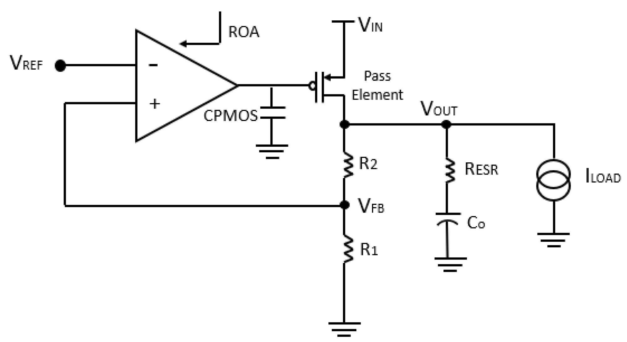
Figure 3.
Architecture of folded cascode op-amp.
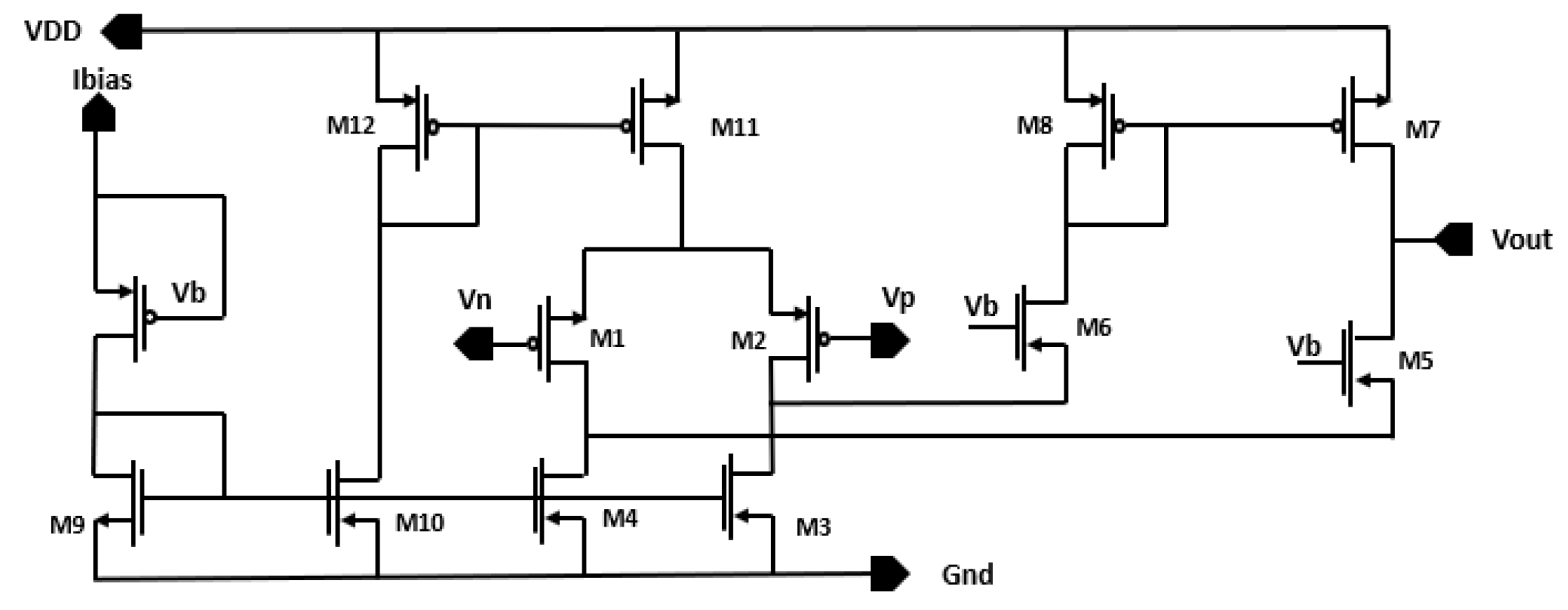
Figure 4.
LDO with noise sources.
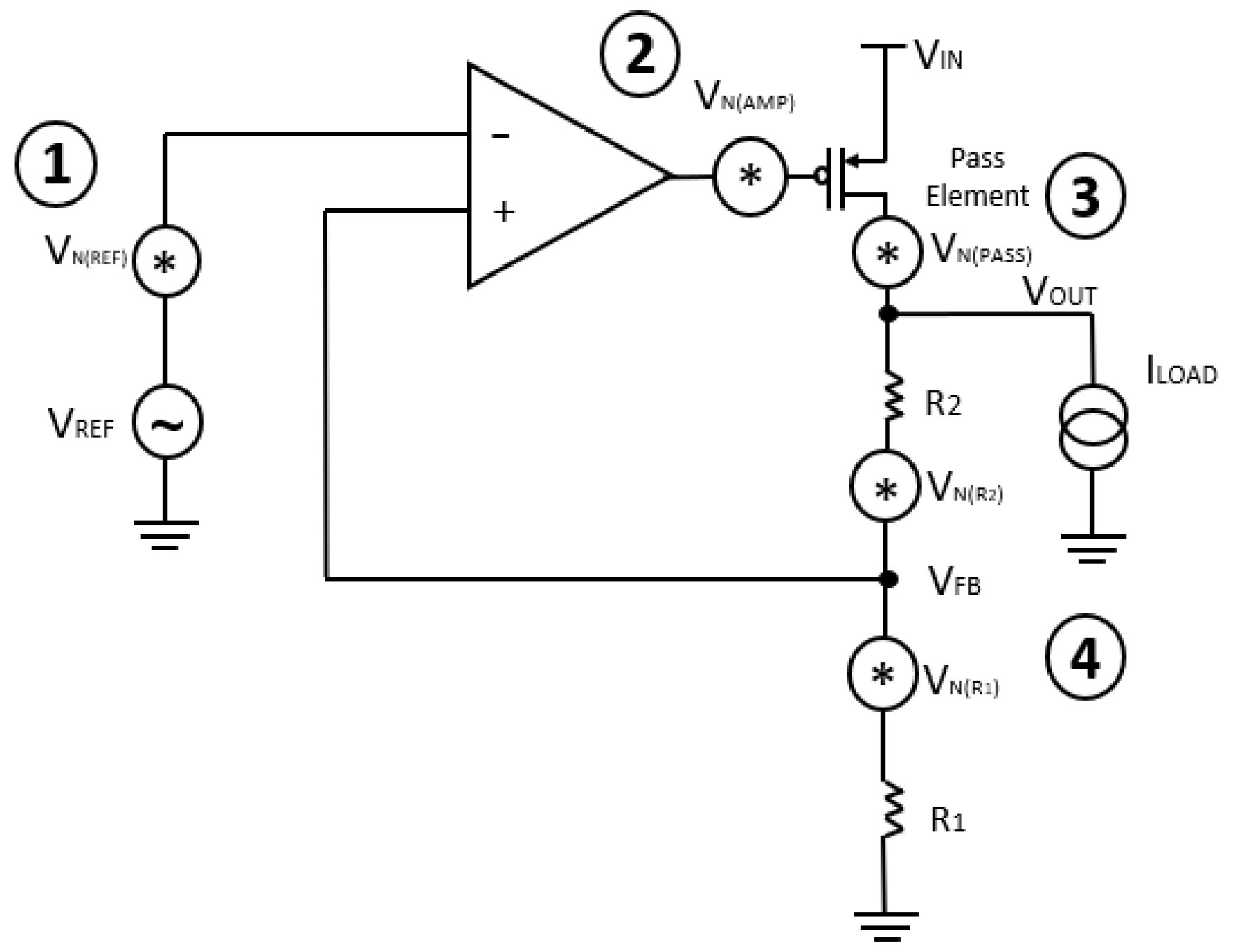
Figure 6.
Selected architecture of op-amp.
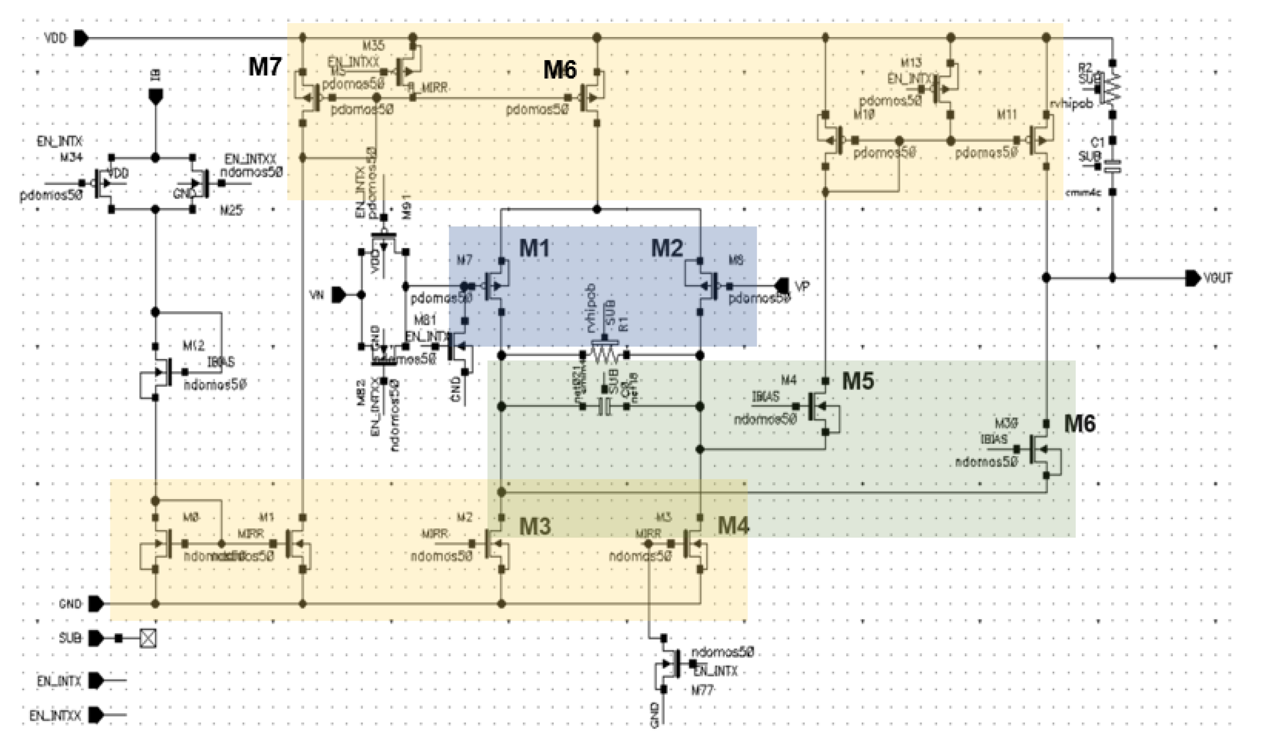
Figure 7.
LDO with enabling circuit.
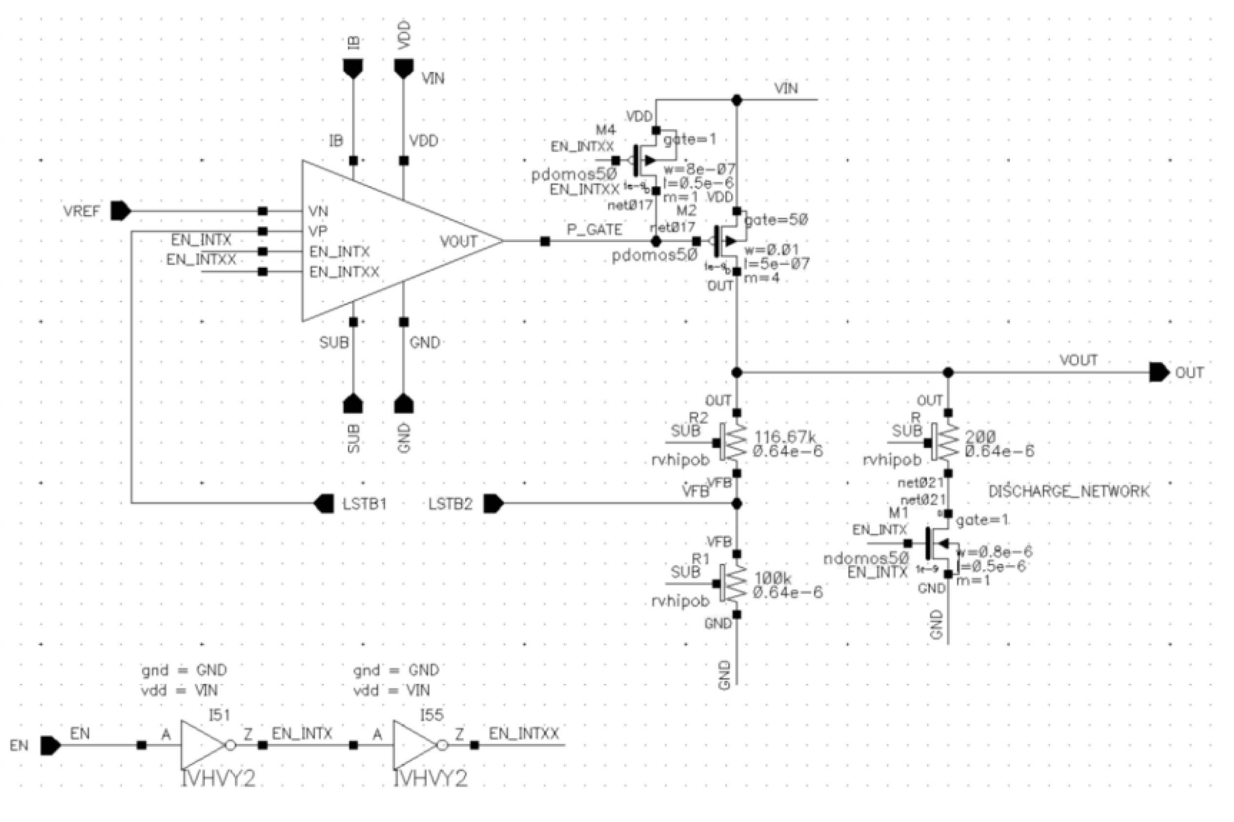
Figure 8.
Op-amp with shut down network.
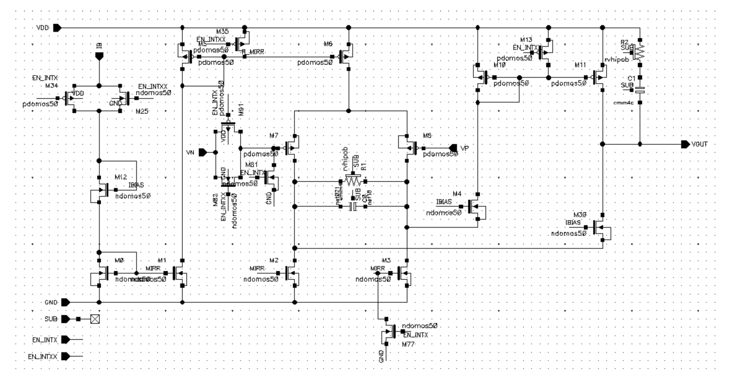
Figure 9.
Test bench for current limiter protection circuit.
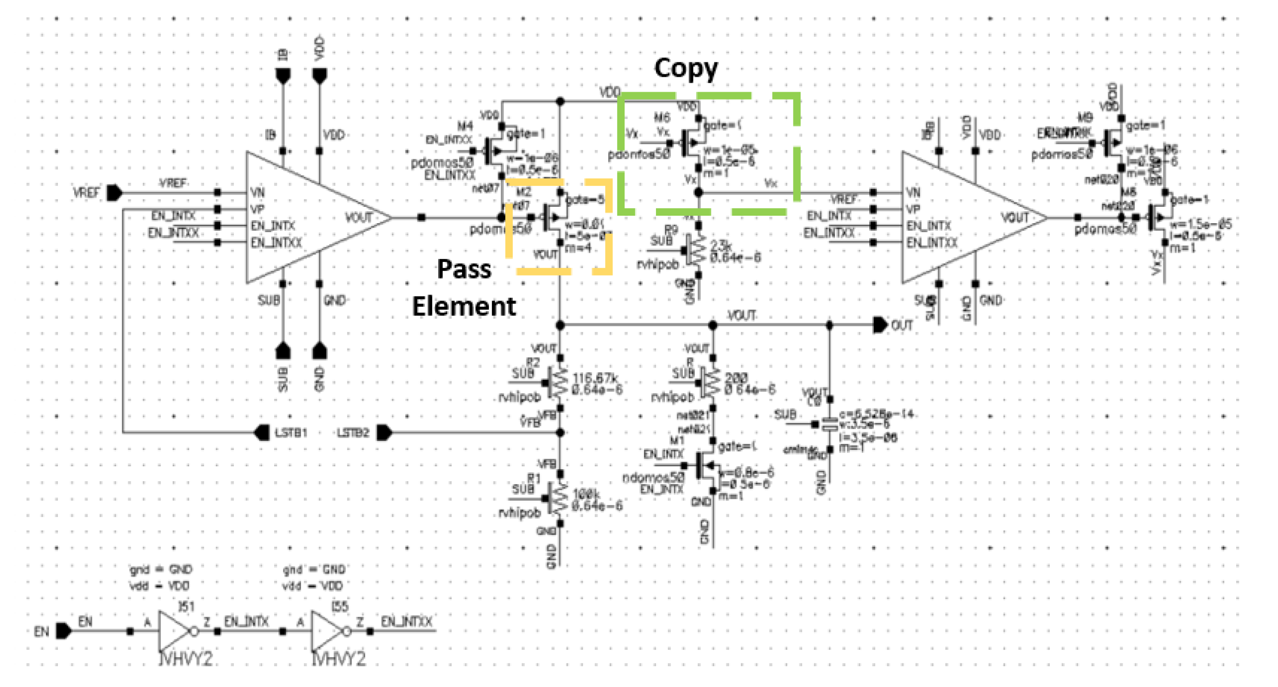
Figure 10.
Output noise vs frequency.
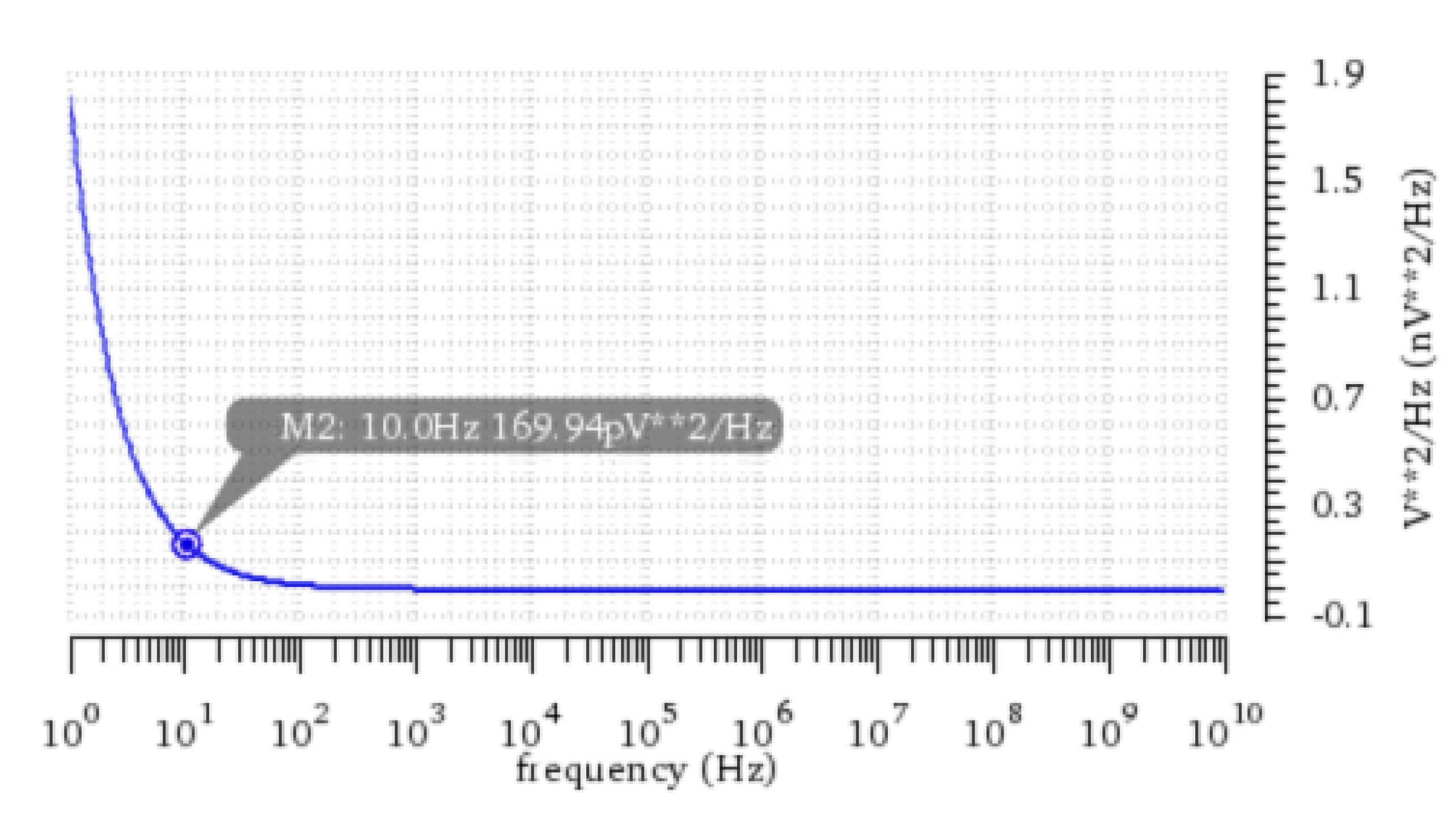
Figure 11.
Frequency Response of LDO.
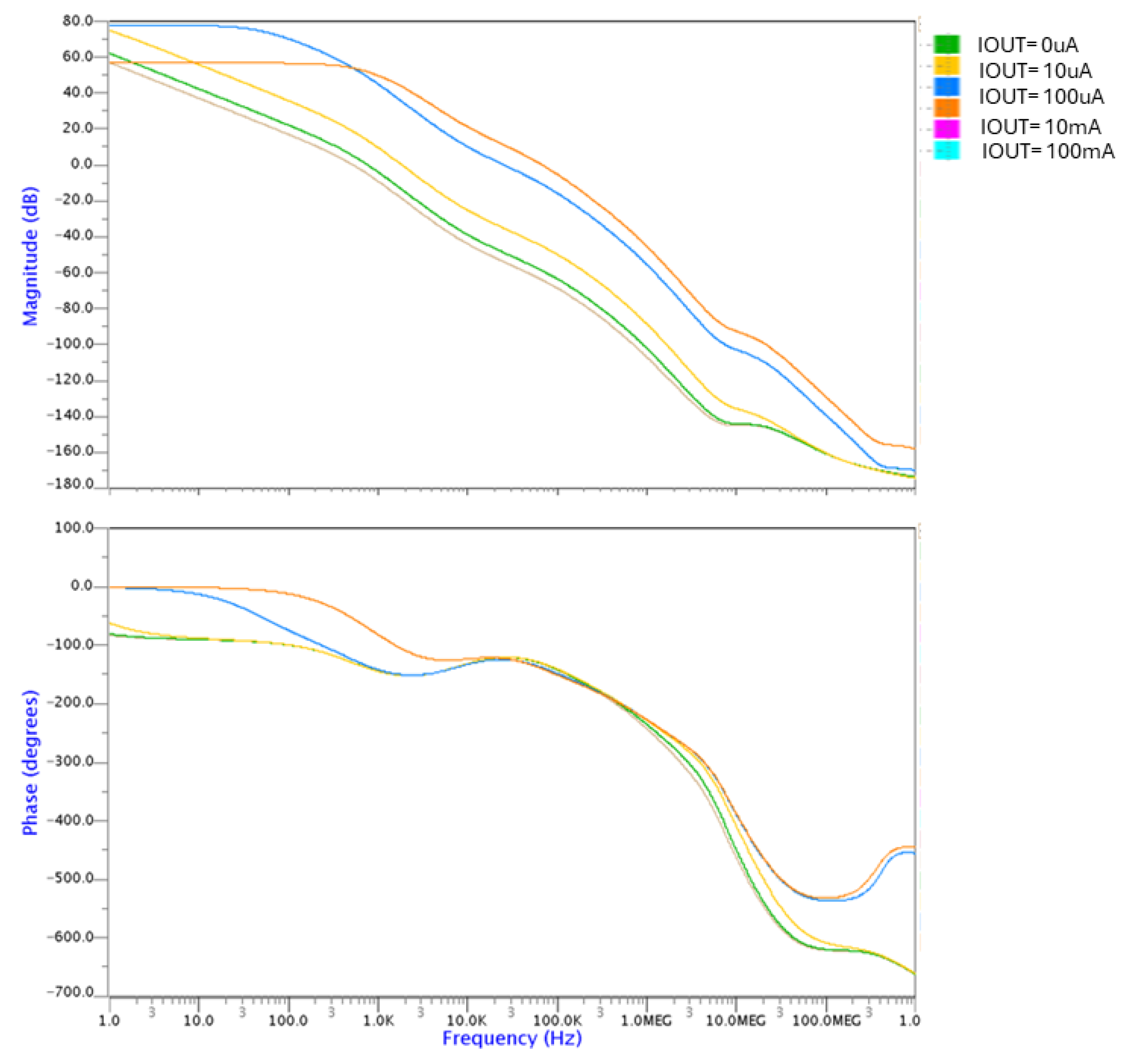
Figure 12.
Transient Response at different temperatures and corners.
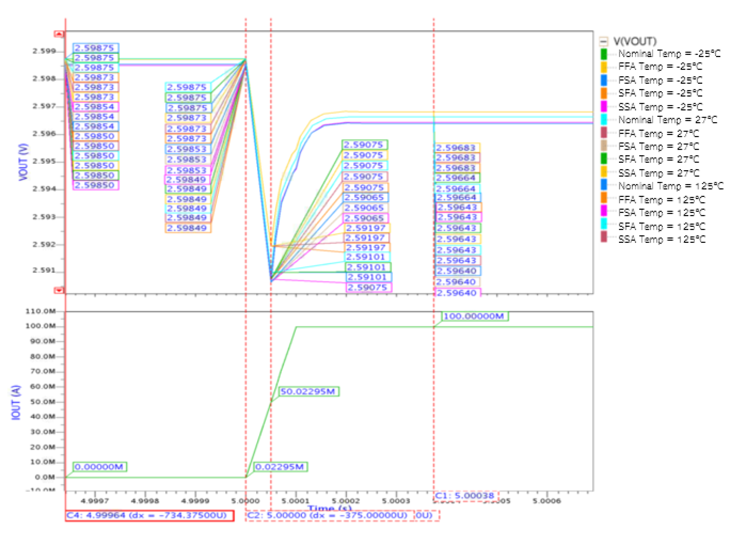
Figure 13.
Power dissipation vs output current.
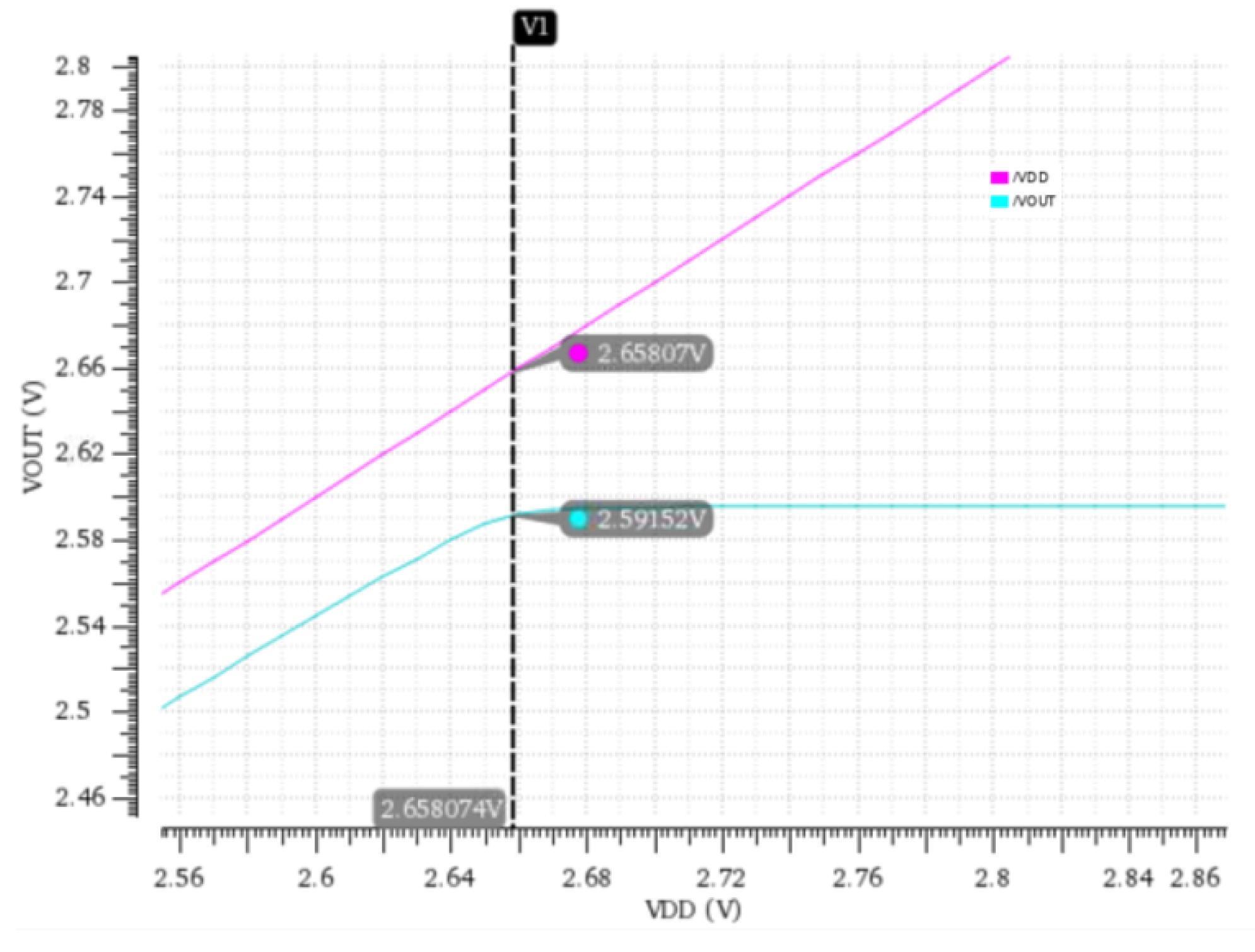
Figure 14.
Power dissipation vs output current
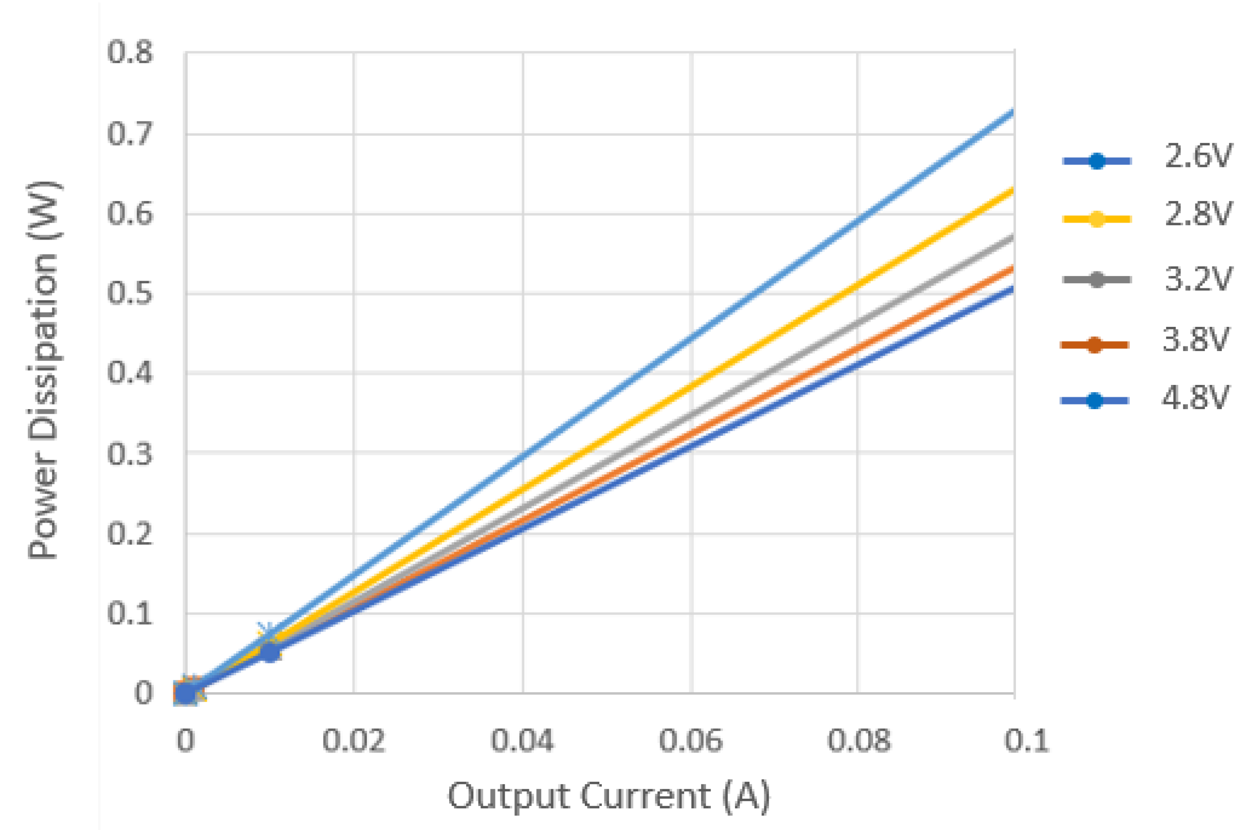
Figure 15.
PM and GM at different Vin and Iout, (a) Phase margin versus Iout at different Vin, (b) Gain margin versus Iout at different Vin, (c) Phase margin versus Vin at different Iout, (d) Gain margin versus Vin at different Iout
Figure 15.
PM and GM at different Vin and Iout, (a) Phase margin versus Iout at different Vin, (b) Gain margin versus Iout at different Vin, (c) Phase margin versus Vin at different Iout, (d) Gain margin versus Vin at different Iout
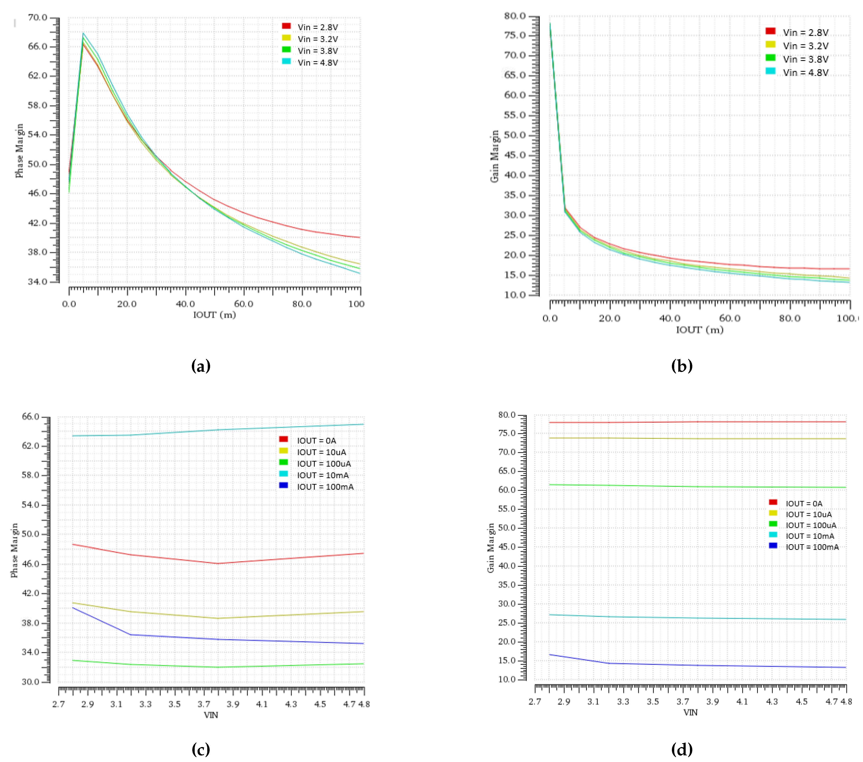
Table 1.
Aspect Ratio of Pass Element
| Width (mm) | Length ( m) | No. of devices |
|---|---|---|
| 10 | 0.5 | 4 |
Table 2.
Aspect Ratios of op-amp MOSFETs.
| Transistor | W/L |
|---|---|
| W=15 m, L=3 m | |
| W=4 m, L=5 m | |
| W=3 m, L=1 m |
Disclaimer/Publisher’s Note: The statements, opinions and data contained in all publications are solely those of the individual author(s) and contributor(s) and not of MDPI and/or the editor(s). MDPI and/or the editor(s) disclaim responsibility for any injury to people or property resulting from any ideas, methods, instructions or products referred to in the content. |
© 2024 by the authors. Licensee MDPI, Basel, Switzerland. This article is an open access article distributed under the terms and conditions of the Creative Commons Attribution (CC BY) license (http://creativecommons.org/licenses/by/4.0/).
Copyright: This open access article is published under a Creative Commons CC BY 4.0 license, which permit the free download, distribution, and reuse, provided that the author and preprint are cited in any reuse.


