
Submitted:
10 July 2024
Posted:
11 July 2024
You are already at the latest version
Abstract
Electromagnetic interference (EMI) generated by switching operations within high voltage DC (HVDC) converter stations is an issue that has been addressed by CIGRE and methods to manage EMI should be considered in the design phase using electromagnetic modeling techniques. It is shown that method of moments-based techniques that have been used in many previous studies may not be sufficient. Here, the finite-difference time-domain method is used to study the properties of single switching events using a realistic model of an HVDC converter station with special emphasis on determining the impact of the valve hall on shielding EMI. It is shown that the valve hall does not confine high frequency electromagnetic fields to the valve hall; rather it delays them from exiting through bushings in the wall. Further, it is shown that incorporating electromagnetic absorbing material into the valve hall design can significantly reduce EMI outside the converter station.
Keywords:
HVDC
; converter station
; valve hall
; EMI
; RFI
; FDTD
; MoM
1. Introduction
Electromagnetic interference (EMI) due to high voltage direct current (HVDC) converter stations or flexible alternating current transmission systems (FACTS) installations has been a subject of interest for many years. There are several distinct sources of EMI associated with these including corona-initiated noise from conductors and other hardware, spark discharges due to arcs between hardware at different space potentials, and commutation noise due to the current switching operations of power electronic devices. Here, the emphasis will be on the EMI due to switching operations in HVDC converter stations. Limits on EMI generated by these stations have been proposed by CIGRE [1]. Further, these limits have often been adopted by companies that employ HVDC converter stations within their electrical transmission network [2]. Hence, without measures to suppress EMI, the stations may not comply with the limits required by the companies that purchase them. One possible consequence is significant economic impact in terms of delays and contractual penalties.
Over the years, the technology used in power electronics has evolved. For example, many modern converter stations are based on modular multilevel converter technology that incorporates insulated gate bipolar transistors (IGBTs) to switch current. These IGBTs have switching times on the order of 100 ns; much shorter than those of the thyristors they have replaced. Although the CIGRE EMI limits are defined up to 18 GHz, the IGBT switching speed will limit the frequencies of interest to below approximately 30 MHz. This assumption has been validated by the statement in a later CIGRE paper [3]. “Above 30 MHz it is not possible to distinguish the level generated by the installation from the background noise level.”
Along with proposing EMI limits, the CIGRE Guide has described methods to be used to measure EMI (e.g., antenna and detector types including peak and quasi-peak) [1]. In addition, guidance is provided for interpreting measurements since EMI from other sources generally exists and must be separated from that generated by HVDC converter stations [1].
Generally, when HVDC converter station vendors propose equipment for these facilities, they are required to predict EMI and will want to ensure that the EMI meets CIGRE limits at this stage. Further, since these stations are expensive and time consuming to construct or modify, modeling EMI is required to reduce the cost and time needed to meet EMI limits.
Given this background, a considerable amount of literature has been published in the area of electromagnetic modeling of HVDC converter stations. Of necessity, these models utilize numerical modeling techniques given the complexity of the stations. In fact, in Sec. 6.1 of the CIGRE Guide it is noted that [1], “Describing an electromagnetic complex environment like the one of an electric substation is very complicated not only for the model itself, but mainly for the difficulty in knowing, even with rough precision, all the sources of electromagnetic field contained inside the fence circumscribing the area relevant to the substation…”
There are three components to the model. The first is to define the fundamental source(s) of the EMI. The second is to construct a model that accounts for the propagation of EMI currents throughout the HVDC converter station. This model will account for various components such as transformers, the smoothing reactor and the filters (if any). Appropriate techniques (e.g., circuit theory, transmission line theory, and full wave theory) are used depending on the distances involved relative to the appropriate wavelength. Finally, the source currents can be used for calculating the electric and magnetic fields in the vicinity of the HVDC converter station. This model should include the effect of shielding provided by the valve hall.
The specific characteristics of EMI sources within a station are not the subject of this paper because they are usually proprietary to a given manufacturer. Rather, the disposition of electromagnetic energy generated by these sources will be carefully examined1. One specific issue of interest is the impact of the of the valve hall construction. Part of the reason for this comes from the comment in Sec. 5.2 of the CIGRE Guide [1], “If the power electronic equipment is installed in a metallic building, or a building with metallic structures, the building will screen the radiation from the power electronic equipment by the induced compensating currents in the conducting metallic parts. The level of RFI [radio frequency interference] is reduced.” In this statement, there is no discussion about the attenuation and frequency variation of the shield, the effect of openings in the shield for connections of the AC and DC sides to the outside, or the ultimate disposition of the electromagnetic energy confined within the valve hall. Yet these topics are critical issues in determining the measured EMI at specified distances from the installation. They are also the major issues discussed in this paper.
1.1. Previous Research
Given the purpose of this paper, the following discussion of previous research identifies the relevance (or not) of each paper to the impact of valve hall shielding or other impacts on reducing EMI. The earliest reported research on this topic is that of Hylten-Cavallius and Olsson in 1962 [4]. The next was work reported by Annestrand in 1972 [5]. There, measurements were reported of EMI from the switchyard and along transmission lines. In addition, the attenuation of a valve hall was measured before equipment was installed. From [5], “The effectiveness of the valve hall screen at Celilo was verified before equipment was installed in the valve hall. A noise generator, essentially a vertical electric dipole, was erected in the valve hall and the noise level measured as a function of distance from the source. The dip in the profile at the wall screen was taken as a measure of the attenuation… In the frequency from to 5 MHz range an attenuation of 40 to 45 dB was measured.” Soon after this, Sarma2 and Gilsig reported their work on calculating EMI from HVDC converter stations [6]. They discussed the source of the EMI as the transient change in voltage across the terminals of a valve. Then, they calculated the high frequency transient currents in the converter station using appropriate high frequency equivalent circuits for different elements of the network. Comments are made about the effectiveness of inductive filters (15 to 20 dB reduction). These currents are then used to calculate the EMI fields in the vicinity of the station.
In the 1980’s, a large EPRI project was conducted to better understand the EMI from HVDC converter stations [7,8,9,10]. In this project, a scale model of an HVDC converter station was developed and used for measurements. Further, an EMI prediction program was developed using wideband circuit equivalents for components [8]. One relevant result was that [9], “the study showed that if the smoothing reactor is in the HVDC bus, it does attenuate the RF signal on the HVDC bus significantly.” There was no attempt to model shielding of the valve hall.
In 1989, Dallaire and Maruvada [11], rather than producing a full analysis of a converter station, applied the full-wave analysis using the method of moments to evaluate the effectiveness of traditional shielding and filtering techniques. This is a useful reference for at least two reasons: (1) Specific high frequency equivalent circuits of components are identified and (2) the results could potentially be used to identify the relative effectiveness of shielding and filtering. It was shown that there are situations in which the radiated field in a particular direction may actually be enhanced because of the shielding enclosure [11]. This stands in contrast, for example, to the blanket statements in [5,12] that indicate a value hall will provide at least 40 dB of reduced radiation. The statements in [5,12] are based on measurements and they do not provide a full-wave analysis of the electromagnetic environment representative of an actual valve hall. Later, Maruvada, Malewski, and Wong reported measurements of the electromagnetic environment, but no modeling [13].
In 1999, Murata et al. built a 1/400 scale model of an HVDC converter station and analyzed it using the method of moments in the frequency range 200–1000 MHz [14]. Included in the model were busses, equivalent circuits of devices such as DC reactors, the valve hall, and other buildings. No details were provided about the meshing or about how openings in the valve hall through which the busses passed were (if they were) modeled, however, calculated and measured fields were reasonably close.
In 2006, Juhlin et al. provided useful information about background noise as well as characteristics of different sources of EMI attributable to HVDC converter stations [3]. These include corona and sparking in addition to commutation noise. Several measurement results are given for points near HVDC converter stations, but no modeling was done.
In two papers that appeared in 2007 and another in 2009, Yu and various colleagues [15,16,17] described a complete circuit of the converter station including wideband equivalent circuits for components such as the smoothing reactor as well as parasitic elements. The entire circuit was evaluated using lumped circuit theory. Hence, the results are not likely to be valid at higher frequencies since at 30 MHz the wavelength is 10 meters and distances are no longer small compared to a wavelength. No attempt was made to model the shielding of the valve hall. Similarly, no attempt was made to model the valve hall shielding in a 2016 paper by Sun, Cui, and Du [18] or in the 2020 work of Wei, Wang, and Zou [19].
In a 2019 ABB Review article, it was reported that, “ABB’s smart simulation models, or digital twins, reproduce the entire converter stations including valves, valve hall, converter reactors, wall bushings, converter transformers, high frequency (HF) filters and the entire wiring in the AC- and DC-yards” [20]. While details of the modeling are not given in this article, some information about their models has been published in [2,21,22]. The simulations were performed in the CST Studio Suite using the transmission line matrix (TLM) time domain solver with broadband circuit models for the smoothing reactors and transformers. It was noted in [2] that the highest frequency of interest was 10 MHz. However, while the comparison between simulation and measurements reported in their Fig. 17 was generally good, there are significant differences at some frequencies below 10 MHz and the measurements in the range above 10 MHz suggest that some attention to modeling in this range is warranted. Further, in [20] it is noted that bushings, doors, vents and possible deficiencies in wall construction will reduce the shielding efficiency because they create openings in the Faraday cage. These issues will be visited in this paper.
Most recently, Ning et al. have developed a model for calculating the electromagnetic radiation of the converter valve based on the method of moments [25]. This model has been used to study the interaction between the converter valve and its operating system. It does not report any calculations of EMI outside the station.
2. Materials and Methods
Simulations were performed using the method of moments (MoM) and the finite-difference time-domain (FDTD) method. The MoM simulations employed the NEC-5 software [29,30]. The FDTD code was developed in-house. The software that was used is a varients of that described in [23] and is available from GitHub [24].
3. Results
3.1. The Method of Moments: Attributes and Limitations
One approach to modeling a substation as suggested by CIGRE is to use a large number of dipoles [1]. However, the surfaces, such as the metallic shielding surfaces that surround a valve hall, are not readily modeled merely by dipoles. Given this, several authors have modeled substations using the method of moments (MoM) which provides a method for describing the electromagnetic fields about a collection of conductors with specified sources [12,14,15,16,17,18,26,27,28]. The conductors are divided into small segments (effectively acting like dipoles) or surface patches (thus permitting the modeling of conducting enclosures such as associated with a valve hall). MoM is inherently a frequency-domain technique and thus the transient nature of sources in an HVDC station must be accounted for by specifying the correct magnitude and phase of the spectral components of the excitation and transforming to the time domain. The MoM does have several compelling attributes in terms of its modeling abilities. First, it permits simple and accurate modeling of thin conductors such as one would find throughout an HVDC converter station. Additionally, one can easily incorporate lumped elements at a point in a line or distribute a load over some portion of the line. But, caution must be exercised when modeling using a lumped circuit since it may require that physical elements of the structure responsible for the lumped circuit behavior be eliminated. Finally, one need only determine the currents that flow on wires and surfaces. Once these are obtained, the fields can be obtained throughout space.
MoM was used by Dallaire and Maruvada [11] to show that it is critically important to conduct a full-wave model of the enclosure with the associated conductors passing through the shielding. As mentioned, they showed that there are situations in which the radiated field in a particular direction may be enhanced because of the shielding enclosure [11]. As also mentioned, this contrasts, for example, with the statements in [5,12] that indicate a value hall provides at least 40 dB of reduced radiation. Again, the statements in [5,12] are based on measurements and the authors do not provide a full-wave analysis of the electromagnetic environment representative of an actual valve hall.
Since MoM has frequently been used to model emissions from converter stations, it was decided to explore the degree to which the most recent version of the MoM-based NEC code, i.e., NEC-5, could be expected to yield meaningful results for scenarios related to HVDC converter stations [29,30]. More specifically, a simple test where a dipole source was enclosed in a simplified valve hall represented by a hollow metallic cube 10 m to the side. The dipole was aligned with the axes of the cube and centered in two of the dimensions but offset from the center by 3 m in one of the dimensions. The valve hall was “perfect” in that there were no holes in its walls nor conductors passing from the inside to the outside. The magnitude of the electric field was recorded over a circle that was 200 m in radius and centered about the z axis. If the numeric code was performing perfectly, the exterior fields would be identically zero at all points throughout space exterior to the cube. However, that was not the result that was obtained.
Since the MoM is a numerical method and the currents on the patches that represent the walls of the enclosure are discretized, the currents are always approximations and one would not expect perfect cancellation exterior to the enclosure. Realistically, the best that one could hope for is that the exterior fields should be “small,” but what constitutes “small” and the degree to which MoM can achieve that appears open to question. In many applications, when comparing numerical results to either theoretical or measured results, an error of one percent is quite acceptable. Another way of thinking of one percent is two orders of magnitude or 40 dB. But in the scenario described above, with a source in a perfect valve hall, where the exterior field should be zero, the difference between any non-zero field and the correct value is infinite on a dB scale. Alternatively, one might compare the “numerically leaked” field at the exterior compared to the field when no valve hall is present. This was done for excitation frequencies of 200 kHz, 1 MHz, 5 MHz, and 25 MHz. Table 1 shows the reduction of the measured field caused by the valve hall compared to when the valve hall is not present (a finitely conducting ground beneath the perfect valve hall is present for all calculations with , mS/m).
Because the hall has no apertures, the correct change is on a dB scale, i.e., the lower the value the better. At 200 kHz we note that the reduction is on the order of 40 dB which is the value often given as the effect of the valve hall. Recall that a 40 dB reduction appears in [5,12] and was based on measurement. However, the approximate 40 dB reduction observed at 200 kHz with this NEC-5 simulation is purely a numeric artifact. The fact that this may agree with measurement should be considered coincidental and not indicative of this software capturing the full physics of the effect of the valve hall. In [30] the authors also report “shielding effectiveness” at 15 MHz of dB. That matches the value for 5 MHz in Table 1 remarkably closely. But, again, this is mere coincidence. If one continues to higher frequencies (up to 100 MHz), [12] reports the shielding effectiveness further increases to dB whereas the MoM results mysteriously drop to dB at 25 MHz (the highest frequency that was considered). In contrast to the behavior at these frequencies, the results obtained at 25 MHz are unacceptably high (predicting only about dB of shielding from the perfect valve hall) and apparently nearly immune to an increase in discretization of the valve hall walls. This is a cause for concern and at present we have no suitable explanation for this behavior.
The results in Table 1 were obtained using a discretization that adheres to the recommendations in the user’s manual [30]. Nevertheless, keeping in mind that any non-zero field represents an error and observing that results ran into difficulties at 25 MHz, the test was run using a finer discretization. The results in Table 1 were obtained using 400 patches per face of the cube (i.e., 20 patches along a side of the cube for patches). There was no significant difference in the results.
3.2. The Finite-Difference Time-Domain Method: Initial Insights from Simple Geometries
The finite-difference time-domain (FDTD) method [31,32] employs a fundamentally different approach. One must discretize not only the sources themselves, but also the space in the vicinity of the sources and the space that surrounds any physical features that might affect the field of interest. In addition to discretizing space (where the discretization assigns the appropriate material properties at each point in the discretization), the FDTD method also discretizes time. In this way all the derivatives in Maxwell’s equations (specifically the curl equations) are replaced with central differences. This yields a set of equations where future (unknown) fields are expressed in terms of past (known) fields. One then advances by incremental steps in time, revealing the time-domain behavior of the fields. While the MoM is a frequency-domain technique that allows one to obtain the fields throughout space at a single frequency, FDTD is a time-domain technique that can potentially yield results over a broad spectrum with a single simulation. However, FDTD will only directly yield the fields within the space that has been discretized. If one is interested in fields outside of the discretized space, one must do a transformation of the known fields to the point of interest. FDTD is generally considered to be quite computationally demanding. Furthermore, special consideration is needed to handle any number of features of a particular scenario such as having a relevant physical structure that is small compared to the discretization that is used.
Several FDTD simulations were run using code developed in-house that explored various aspects of HVDC converter station modeling with an emphasis on the effect of the valve hall. First considered was a “perfect” valve hall. As with the initial MoM testing, this hall had no openings nor any conductors running from the interior to the exterior. However, instead of using a cube 10 m to the side, the dimensions were based on those of an actual converter station. The valve hall dimensions were (x) 42 m by (y) 68 m by (z) 19 m. The hall and surrounding space were discretized with a step size of m. Initial simulations, which incorporated part of the AC yard and the DC hall (reactor hall), used a computational domain of cells in the x, y, and z directions, respectively.
The computational domain is depicted in Figure 1 where the scale is in terms of FDTD cells (one can divide by two to convert to meters). Red lines correspond to conductors and the rectangular structure near the center of the figures corresponds to the valve hall. Conductors are modeled as a line of electric field nodes set to zero. Several researchers have reported that the “effective” radius of such a line of cells is approximately [33,34,35,36,37], ranging from [33] to [35]. In [33,35,36,37] the researchers proposed ways to modify the FDTD update equations to model wires that had radii that were either smaller or larger than this effective radius. In [38], Taniguchi et al. reexamined the effective radius in the context of surge impedance and compared FDTD results to the theoretical work of Chen [39]. They obtained an effective radius of . This is taken to be most accurate value for the effective radius. Applying that to the modeling performed here yields an effective conductor radius of roughly 10 cm.
The green plane on which the valve hall sits is a perfectly conducting ground plane. Figure 1(a) shows the projection onto the plane (the green ground plane has been removed from this view). The AC yard is to the left (west) of the valve hall. The three lines in the AC yard ultimately are shorted together at what would be, in practice, the location of a transformer. Although this is a crude approximation for the electromagnetic behavior of the transformer at these frequencies, it is not an unreasonable one given the lack of a validated model for the transformer in the open literature. Nevertheless, because of the shorting of the lines at this location, the model presented here could not predicted the high frequency currents on the AC lines exiting the AC yard.
The conductors to the right (east) of the valve hall correspond to several of the lines that exist in the DC hall. The walls of the DC hall are not modeled. The 18 rectangular conductors seen within the valve hall serve as coarse approximations of the valves themselves. No attempt was made to model the detailed physical structure of the valves, but rather to model their overall size and shape to approximate how electromagnetic energy might propagate in their presence. A horizontal line passes through the center of each of the six sets of three “valves,” transitioning from the AC to the DC side of the hall. Figure 1(b) shows the projection of the computational domain onto the plane while Figure 1(c) shows an oblique perspective projection of the computational domain.
Energy is introduced into the computational domain by specifying the electric field at a particular FDTD node along one of the conductors. Specifically, the value of an node along a line that transits from the AC to the DC side of the hall is specified by a source function at each time-step of the simulation. This is equivalent to specifying the voltage at that location. The source function was a unit-amplitude Ricker wavelet. (A Ricker wavelet is obtained by taking the second derivative of a Gaussian. In this way the Ricker wavelet has somewhat similar spectral properties to a Gaussian pulse, but there is no DC component.) The Ricker wavelet had its peak spectral content at 10 MHz. This source can be thought of as introducing energy over a range of frequencies that can be associated with commutation events. But, the simulations are performed with a single “firing” of the Ricker pulse at a single location. For this analysis, the pulse source location is near the right edge of the center “valve” at the northern-most (greatest y) side of the valve hall as shown in Figure 1(a).
Although the computational domain is finite, an infinite space is approximated by surrounding the computational domain in a convolutional perfectly matched layer [40]. Simulations were typically run for time steps. For the discretization that was used, where the time step was ps, this corresponds to a total of s. (The Courant number was the 3D limit of .)
In FDTD, boundary conditions at material interfaces “take care of themselves” as one merely specifies material properties at all points throughout the discretized space, i.e., throughout the FDTD grid, and then advances in time via the discretized version of Maxwell’s equations. However, perfect electric conductors (or nearly perfect conductors) such as those that pertain with the metal walls of a valve hall, are realized not by specifying material values, per se, but rather by setting the electric fields tangential to such conductors to zero and leaving them zero. (This is similar to the way in which conductors are realized where a line of electric field nodes is set to zero.)
Simulations were performed of a perfectly intact valve hall where, although the conductors (red lines) shown in Figure 1 are present, they are terminated by unbroken conducting walls. The FDTD model of such an intact valve hall yields results consistent with expectations: (1) In contrast to the MoM solution, the fields exterior to the hall are identically zero. (2) Once energy is introduced into the valve hall, either in the form of fields that radiate away from the source or currents induced on the line in which the source is embedded (and the fields associated with such currents), this energy simply oscillates inside the hall until the simulation is terminated. (3) Strong resonances occur owing to the structure of the hall and the associated interior conductors. When the model consists solely of perfectly conducting wires and walls, there is no loss mechanism and the fields resonate indefinitely in this rectangular cuboid. (The simulation does allow for loss in the form of radiation and subsequent absorption in the perfectly matched layer that surrounds the computational domain. However, such loss can only take place if fields escape the valve hall. And, with the hall intact, no fields escape.)
Nine holes were then introduced into the valve hall walls corresponding to the locations of each of the lines seen in Figure 1 transitioning from the interior to the exterior of the valve hall (three on the AC side of the hall and six on the DC side). The size of the holes was not the minimum possible, but rather the minimum possible that could subsequently model a conductor passing through the hole. For the somewhat coarse discretization that was used ( m), the hole could be said to be approximately 1 m in diameter. Given the peak spectrum of the pulsed excitation was at 10 MHz, i.e., a wavelength of 30 m, the holes were small compared to the wavelength of the bulk of the excitation.
With the holes thus created, multiple simulations were performed with various modifications. First, in addition to introducing the holes, a 2 m section of each conductor passing through the walls was removed that was centered about the valve hall walls, i.e., a 1 m section of each conductor was removed to either side of the wall it passes through. Second, the conductors were left intact and merely passed through the holes. For both simulations, the magnitude of the electric field at two points were recorded, one point inside the hall and a point outside. These points were selected somewhat arbitrarily. Relative to the hole that was introduced to accommodate the northern-most line in Figure 1(a) that passes from the valve hall to the DC hall, the “inside point” was 4 m away in x (i.e., 4 m further into the hall relative to the wall with the hole), 3 m away from the hole in y (3 m closer to the center of the hall), and 2 m below the hole in the z direction. The outside point was 4 m away in x (i.e., 4 m away from the wall), but as with the inside point, 3 m away in y, and 2 m away (below) in z. Thus, each observation point was approximate m away from the hole. This northern-most line is also the one along which the commutation event is simulated.
Figure 2(a) shows the field measured3 at the inside and outside points when the 2 m segments are removed from each line. The fields are plotted on a log scale over the first 5 s of the simulation. Note that the field inside the hall becomes non-zero prior to the field outside the hall owing to its closer proximity to the source. The field inside the hall varies in the vicinity of roughly db while the field outside the hall varies in the vicinity of roughly db, i.e., a reduction in the field of approximately 50 db.
Figure 2(b) shows the field at the same two points, using the same excitation and the same geometry, but now the conductors are intact that transition through the holes in the valve hall walls. Again, the field arrives at the exterior point after arriving at the interior point. However, in this case the fields are almost comparable in magnitude. The inside field is generally larger, as would be anticipated, but only slightly so and there are instances where the field at the point outside the hall is greater than inside the hall. Another way to think about the contrast between Figure 2(a) and Figure 2(b) is that having the intact conductors raises the field exterior to the hall by approximately 50 dB.
The simulation for Figure 2(b) merely had the conductors passing through the holes surrounded by free space. Another simulation was performed that modeled bushings associated with each hole. These bushing were assumed to be cylindrical, extend 1 m to either side of the wall, and have relative permittivity, , of 3. The radius of the bushings was such that it filled the holes through which the conductors passed. The bushing made essentially no difference to the overall observed behavior seen without the bushings. Another simulation was performed where, in addition to having the bushings present, lumped-elements inductors were incorporated into the FDTD grid to represent the smoothing reactors found in the DC hall. The inductance used was mH (in keeping with the inductance provided in [21]; the implementation followed the work decribed in [41]). Again, this made effectively no difference in the roughly similar field observed inside and outside the valve hall.
In Figure 2(a) note that after about 1 s the fields decrease very little. Contrast this to the slight, but clearly evident, decrease in the field as time progresses in Figure 2(b). In both simulations there are nine holes in the valve hall walls, but only in the simulation for Figure 2(b) do conductors pass through the holes. In the case of Figure 2(a), given the relatively small size of the holes compared to the wavelength, the fields escaping the hall are primarily evanescent. These fields can couple onto the conductors that are present outside the hall, but this represents a nearly vanishingly small radiation of the fields which explains why there is seemingly no decay (with time) of the fields in Figure 2(a). (Figure 2 only displays the first 5 s of the simulation but this persistence of the field is evident for the entire s simulation.) On the other hand, when the conductors are intact, they serve to create what is effectively a transverse electromagnetic (TEM) transmission line for fields to pass from the interior to the exterior of the valve hall. There is no cut-off frequency for this transmission line (which needs to be the case to get DC and low-frequency energy in and out of the hall).
A conductor above a ground plane serves as a TEM transmission line. The lines in the AC yard can be thought of as segments of such lines. As a line passes through the valve hall wall, one might envision this transit as a very short co-axial line where the conductor is the inner core of the co-axial line and the wall is the outer conductor. There is an impedance mismatch going from one form of transmission line to another, but given the short extent of the intervening “co-axial” line, this mismatch does not cause significant reflections, i.e., fields directed out of the hall largely continue to exit the hall, a point which will be returned to when currents on the conductors are considered.
The component of the electric field at these observation points when the conductors are intact will now be considered. Figure 3(a) shows the log magnitude4 of the Fourier transform of the component of the electric field measured at the points inside and outside the hall over the range of frequencies from 0 to 35 MHz. For reference, the Fourier transform of the source function is also provided. One can see peak energy occurs at 10 MHz. Note that below approximately 14 MHz, there is very little difference between the fields inside and outside the hall and at several frequencies the field outside the hall is greater than inside the hall. For frequencies greater than 14 MHz, the field inside the hall is generally larger than outside the hall. This appears to indicate the valve hall is serving as a filter. However, such an assertion can be called into question, as discussed below. Note that the lowest-order resonant frequency for a valve hall of this size is MHz. The strongest resonances generally occur below this frequency. Thus, these resonances must be associated with the overall structure of the station, including the conductors in the AC yard and DC hall, and not merely with the valve hall itself. As will be seen, these “low frequency” resonances remain rather persistent regardless of what is done to the valve hall.
Consider the fields normalized by the spectral content of the source function as shown in Figure 3(b). Here the similarity of the fields below 14 MHz and the seeming filtering above 14 MHz are somewhat easier to discern. However, also consider the results shown in Figure 3(c) which are identical to those of Figure 3(b) except now the valve hall has been removed.5 Several of the peaks, especially below about 7 MHz remain nearly unchanged. The persistence of these resonances, independent of the existence of the valve hall, indicates they are associated with the conductors throughout the model. For frequencies above this, the results in Figure 3(c) are much “quieter” than they are when the valve hall is present. Consider the “outside” curves in Figure 3(b) and Figure 3(c). Although the curve in Figure 3(b) is much noisier than that of Figure 3(c), the fluctuations in Figure 3(b) appear to be roughly about the “baseline” shown in Figure 3(c). The same cannot be said of the results for the “inside” curves. It is certainly true that the results for the inside point in Figure 3(c) are quieter than for Figure 3(b), but one would not say that the fluctuations in Figure 3(b) are roughly about the curve present in Figure 3(c). Instead, when the valve hall is present, rather than filtering the outside field, its presence tends to elevate the interior field.
Putting these observations together, we can say that the valve hall does not diminish the exterior field but rather it enhances the interior field. Note, however, that this claim pertains to these two particular observation points, and both are in relatively close proximity to the line on which the source pulse exists. Were one to consider an exterior point located close to one of the two walls with no conductors passing through them, the field measured in the presence of the valve hall would certainly be reduced relative to having no hall present. Nevertheless, the interior field is enhanced6 by the presence of the valve hall (independent of where the field is observed in the interior). Because there is no loss present within the valve hall, the only place energy can go after it is introduced into the valve hall is out along the conductors that pass through the valve hall walls, i.e., along the transmission lines out of the hall. At these frequencies, these lines serve as antennas which then radiate fields into the surrounding environment (as will be considered below).
Instead of a component of the electric field, consider the current on a conductor measured both inside and outside the valve hall. The current is obtained by taking the line integral of the magnetic field around the conductor at the desired measurement point. The current was calculated on the same line on which the source exists (the northern-most line exiting the valve hall to the right in Figure 1(a)). The inside and outside measurement points are each 2 m from the wall (with one being inside the valve hall and the other being in the DC hall). Temporal plots of the currents at these points reveals a difference in the arrival time of fluctuations which is consistent with the different location of the observation points. There are some other differences in the currents, but these are generally relatively minor. Rather than showing a temporal plot, Figure 4(a) shows the log magnitude of the normalized spectrum of the currents when the valve hall is present. Figure 4(b) is the same scenario as Figure 4(a) except the value hall has been removed. Although there are some slight differences in the features observed in Figure 3 and Figure 4, overall the results in Figure 4 serve to confirm the statement made in connection with measurement of the electric field: The valve hall does practically nothing in terms of confining high frequency energy to the interior of the valve hall. One could say that the hall serves to redirect energy while not eliminating it (i.e., delaying energy’s eventual escape from the hall). Once a current has been established on a line within the valve hall, if that line exits the valve hall, the current found outside the hall will be nearly the same as inside.
Having established that the valve hall does little in terms of reducing the ultimate escape of high frequency currents and fields, attention is turned to measurements more aligned with those related to compliance. CIGRE [1] is frequently concerned with the fields that exist “200 m from the closest active part of the station.” The computational was extended domain 200 m (400 cells) in the y direction and the field was measured at several observation points that were 200 m “south” of the southern-most valve hall wall depicted in Figure 1(a) (i.e., 400 cells away from the valve hall wall in the y direction). Recall that the entire computational domain sits atop a perfectly conducting ground plane. All components of the electric and magnetic field were measured at 15 different locations with varying x and z values. Observation points were separated 15 m in x and had vertical displacements (z values) either 2, 3, or 4 m above the ground plane. For the discussion that follows, any, or all, of these points could have been selected and lead to the same observations. For the sake of concreteness, however, an observation point was selected that is m to the “west” of the western-most valve hall wall (i.e., the one leading to the AC yard), 200 m south of the southern-most wall, and 2 m above the ground plane.
Figure 5(a) shows the electric field magnitude over the initial 5 s of two simulations, one when the valve hall is present and the other where all the conductors are unchanged, but the valve hall has been removed. Unsurprisingly, when the valve hall is not present, the initial fields are stronger than when the hall is present (refer to the interval between 1 and 2 s). This is a consequence of the fields being free to directly radiate in all directions (other than “down” into the perfectly conducting ground) from the commutation event. However, after this initial burst, the fields without the valve hall drop below those observed when the hall is present. This is because, without the hall present, much of the energy is quickly lost to radiation throughout the surrounding environment. On the other hand, with the hall present (and there being no loss mechanisms contained within the hall) and energy unable to radiate in all directions, the energy confined to the hall can only escape slowly via the conductors which, in turn, serve as antennas to radiate the field to the surrounding environment. As previously mentioned, including inductances (that model the smoothing reactors) and bushings in the simulation has little effect on the radiated field (effecting mostly the phase but not the magnitude).
Two other scenarios were considered. In one, the walls of the valve hall remained in place, but the roof was removed. Potentially this could have directed significant amounts of energy “up” so that this energy would not be present for terrestrial measurements such as at the observation point being considered. However, at the frequencies being considered, it appears the height of the valve hall walls were not sufficient to so direct the energy. Instead, the fields largely diffract over the walls so that the observed fields in this case are similar to having no valve hall present at all and thus these results are not shown here.
The other scenario we considered introduced absorption loss into the valve hall. This took the form of a 2 m thick (in the z direction) dielectric slab adjacent to the ceiling of the intact valve hall. The slab nearly spanned the x and y extent of the hall, being displaced from the walls and roof by m. The slab had a relative permittivity, , of and a conductivity, , of mS/m. Figure 5(b) again shows the electric field magnitude at the observation point over the initial 5 s of two simulations. The results are again shown for an intact valve hall (the same as in Figure 5(a)) but also for the case when the lossy dielectric slab is in valve hall. In this case, the initial fields, in the interval from 1 to 1.5 s, are nearly identical but with the lossless case having slightly higher peaks. However, beyond that, the field for the lossy hall decreases significantly relative to the lossless case.
Figure 6 shows the log magnitude of the normalized spectrum of the x component of the magnetic field for the three scenarios considered in Figure 5. (If is scaled by the impedance of free space, nearly identical results are obtained compared to plotting the spectrum of . In practice the horizontal component of the magnetic field is measured using a loop antenna, which motivates the plotting of in Figure 6.) Across much of the spectrum, when the lossy slab is present the field is less than the other two scenarios and, over certain ranges of frequencies, significantly so. Above approximately 14 MHz, the lossy results are below those of the intact hall by roughly 10 dB. Between 7 MHz and 14 MHz, the difference between these results varies, but the lossy hall consistently out-performs the intact hall in terms of having lower fields. Below 5 MHz, the results are all quite similar. Again, this range of frequencies is largely below the lowest-order resonance for a cuboid the size of the valve hall.
4. Discussion
Electromagnetic interference (EMI) generated by switching operations within high voltage DC (HVDC) converter stations is an issue that has been addressed by CIGRE and methods to manage EMI should be considered in the design phase using electromagnetic modeling techniques. More specifically, CIGRE has proposed guidelines for maximum values of EMI fields.
Investigations into the modeling of high frequency (e.g., 9 kHz – 30 MHz) EMI emissions from an HVDC converter station leads to the conclusion that one must use a full-wave model to be able to capture the complicated physics of the problem over the broad spectrum of excitation that exists. However, work with MoM and the FDTD method points to the fact that there are numerous ways in which such a full-wave model might lead one astray or be rather limited in the information it can provide. For example, it is shown here that MoM calculations of the small fields outside a shielded valve hall may be numerical artifacts rather than accurate results. Although there are various papers that purport to characterize radiation from or into a shielding structure (e.g., [42,43]), to our knowledge there does not appear in the open literature a thorough analysis in which one can be confident that the effects of a valve hall are fully captured.
Here, a realistic model of an HVDC converter station has been developed and analyzed using the FDTD method. The model consists of the (shielded or unshielded) valve hall as well as conductors within it, the AC yard, the DC hall, and the territory surrounding the station so that EMI can be predicted at distant points.
It is often claimed that a valve hall provides perfect (or near perfect) shielding because it is assumed to be a Faraday cage. This is shown here to be true even if there are holes (small compared to a wavelength) in the shield despite claims that small (compared to a wavelength) seams in valve hall construction can cause significant leakage. It is also shown that the spectrum of the field inside the valve hall is greatly influenced by the cavity resonances associated with the cuboid geometry of a valve hall shield.
If, however, conductors penetrate the valve hall wall, significant leakage of the electromagnetic fields within the valve hall to outside occurs. And, in practice there must be conductors that pass through bushings uninterrupted from the interior to the exterior to carry the AC and DC currents into and out of the valve hall. Hence, the valve hall must be considered “leaky.” It is shown here that the difference between fields inside and outside the valve hall with and without conductors that penetrate holes in the shield can be on the order of 50 dB.
To understand what happens to high frequency electromagnetic energy generated by commutation events in a valve hall, it must first be noted that this energy is dissipated only by absorption in lossy materials or radiation to infinity. A shielded valve hall by itself (i.e., without absorbing material or conductors penetrating its walls) merely serves to trap radiated fields; it is shown here that they reflect around the valve hall indefinitely. If conductors inside the valve hall that penetrate its walls are introduced into the model, the interior fields can and will eventually couple onto these conductors as a means of escape. Once a current is induced on a line, the valve hall does little to filter the current from passing out of the hall. The result of this process is that the original pulse of EMI energy is spread out over a significant amount of time. After it exits the valve hall, it is radiated to infinity. It is this radiation that is the subject of CIGRE guidelines.
A converter station can be envisioned as a source of high frequency energy (owing to the commutations) where this source is surrounded by a lossless shield (the valve hall) that redirects the flow of this energy. Rather than radiating directly away from the source, the valve hall walls redirect any radiated energy back into the interior until it eventually manages to escape via the conductors that pass through the walls. The energy could be said to be temporarily trapped within the hall. However, if a loss mechanism exists within the hall, it becomes possible to absorb this trapped energy before it has a chance to escape and radiate to the surrounding environment.
It is shown here that adding electromagnetic absorbing material only in the vicinity of the ceiling of the valve hall can considerably reduce the EMI energy in the valve hall before it exits via conductors that penetrate its walls. As a result, the radiated EMI outside the valve hall is significantly reduced. It should be noted that this calculation is simply an illustration of what can be done. No attempt has been made to optimize either the electrical properties of the absorbing material, its geometry, or its location within the valve hall. This would be a fruitful endeavor.
Note that the results presented here concerned a single “commutation event” and the focus was on the high-frequency radiation association with that. No definitive claims were made about the precise field that might be measured for such an event. Rather, the goal was to better understand the degree to which the valve hall does or does not prevent fields generated from such an event escaping to locations where their presence may be problematic. In practice, in a modern voltage source converter (VSC) station, thousands of commutations may be occurring in ways that have overlapping and interacting fields. The issue of multiple and interacting commutations will be the subject of future work.
Given all the complexity of an HVDC station, although full-wave modeling is necessary, it is by no means sufficient. It can provide clues and insights into the behavior of various aspects of a converter station, but it cannot be trusted, by itself, to tell the full story. Base-level modeling of sufficiently complicated structures that mimic relevant interacting components of an HVDC converter station needs to be validated by actual measurements. Having validated the model, some level of changing the components of the models to guide design is certainly reasonable. However, it would be completely unreasonable, as appears to have been the case in some previous work, to obtain results from a model and then assume that the introduction of a valve hall that was not previously included in the model will provide a further reduction of, for instance, 40 dB in the radiated fields.
Funding
This research was funded by the Electric Power Research Institute.
Conflicts of Interest
The authors declare no conflicts of interest. The funders had no role in the design of the study; in the collection, analyses, or interpretation of data; in the writing of the manuscript; or in the decision to publish the results.
Abbreviations
The following abbreviations are used in this manuscript:
| AC | Alternating current |
| CIGRE | Conseil International des Grands Réseaux Electriques (Council on Large Electric Systems) |
| DC | Direct current |
| EMI | Electromagnetic interference |
| EPRI | Electric Power Research Institute |
| FACTS | Flexible AC transmission systems |
| FDTD | Finite-difference time-domain |
| HVDC | High voltage direct current |
| IGBT | Insulated gate bipolar transistors |
| MoM | Method of moments |
| NEC | Numerical Electromagnetics Code |
| RFI | Radio frequency interference |
| TEM | Transverse electromagnetic |
References
- CIGRE, Guide for Measurement of Radio Frequency Interference from HV and MV Substations, 2009, ISBN: 978-2-85873-078-0.
- Cottet, D.; Eriksson, G.; Ostrogorska, M.; Skansens, J.; Wunsch, M.; Grecki, F.; Piasecki, W.; Andersson, O. Electromagnetic modeling of high voltage multi-level converter substations, in Proc. of the Asia-Pacific Intl. Electromagnetic Compatibility (APEMC) Symposium, Singapore, May, 2018, 1001–1006. [CrossRef]
- Juhlin, L.-E.; Larsson, T.; Skansen, J.; Petersson, E. Considerations Regarding RI Limits for High Voltage HVDC or FACTS Stations, CIGRE Paper B4-207, 2006.
- Hylten-Cavallius, N.; Olsson, E. Radio Noise from Terminal Equipment of High Voltage Direct Current Systems. Direct Current 1962, 172–181. [Google Scholar]
- Annestrand, S.A. Radio Interference from HVDC Converter Stations. IEEE Trans. on Power Apparatus and Systems 1972, PAS-91, 874–882. [Google Scholar] [CrossRef]
- Sarma, M.P.; Gilsig, T. A Method of Calculating the RI from HVDC Converter Stations. IEEE Trans. on Power Apparatus and Systems 1973, PAS-92, 1009–1018. [Google Scholar] [CrossRef]
- EPRI, Radio Interference from HVDC Converter Stations: Modeling and Characterization, Electric Power Research Institute Report EL 4956, 1986.
- Kasten, D.G.; Caldecott, R.; Sebo, S.A.; Liu, Y. A Computer Program for HVDC Converter Station RF Noise Calculations. IEEE Trans. on Power Delivery 1994, 9, 1129–1136. [Google Scholar] [CrossRef]
- Kasten, D. G.; Liu, Y.; Caldecott, R.; Sebo, S. A. Radio Frequency Performance Analysis of High Voltage DC Converter Stations, IEEE Porto Power Tech Conference, Porto, Portugal, Sep. 2001.
- Caldecott, R.; DeVore, R. V.; Kasten, D. G.; Sebo, S. A.; Wright, S. E. HVDC Converter Station Tests in the 0.1 to 5 MHz Frequency Range. IEEE Trans. on Power Delivery 1988, 3, 971–977. [Google Scholar] [CrossRef]
- Dallaire, R. D.; Maruvada, P. S. Evaluation of the Effectiveness of Shielding and Filtering of HVDC Converter Stations. IEEE Trans.onPowerDelivery 1989, 4, 1469–1475. [Google Scholar] [CrossRef]
- Ding, Z. F.; Liu, L.; Liu, Y. Y.; Liu, X. F.; He, R.; Hu, Y. F.; Jiao, C. Q. Measurement and Analysis on Electromagnetic Shielding Effectiveness of a 500kV UPFC Valve Hall, IEEE 5th International Symposium on Electromagnetic Compatibility (EMC-Beijing), 2017, 1–4. [CrossRef]
- Sarma Maruvada, P.; Malewski, R.; Wong, P.S. Measurement of the Electromagnetic Environment of HVDC Converter Stations. IEEE Trans. on Power Delivery 1989, 4, 1129–1136. [Google Scholar] [CrossRef]
- Murata, Y.; Tanabe, S.; Tadokoro, M.; Ukawa, Y.; Fukunaga, E.; Nakao, H. 3D-MoM Analysis of Radio Frequency Noise Radiation from HVDC Converter Station, IEEE International Symposium on Electromagnetic Compatibility, 1999, Symposium Record (Cat. No.99CH36261).
- Yu, Z.; He, J. L.; Zeng, R.; Zhang, B.; Chen, S. M.; Rao, H.; Zhao, J.; Li, X. L.; Wang, Q. Simulation Analysis on EMI of +-800-kV UHVDC Converter Station, IEEE International Symposium on Electromagnetic Compatibility, 2007, 1–5. [CrossRef]
- Yu, Z.; He, J.; Zhang, B.; Zeng, R.; Chen, S.; Zhao, J.; Wang, Q. Simulation Analysis on Radiated EMI in ±500-kV HVDC Converter Stations, Proceedings of the 18th Int. Zurich Symposium on EMC, Munich, 2007.
- Yu, Z.; He, J.; Zeng, R.; Rao, H.; Li, X.; Wang, Q.; Zhang, B.; Chen, S. Simulation Analysis on Conducted EMD Caused by Valves in ±800-kV UHVDC Converter Station. IEEE Trans. on Electromagnetic Compatibility 2009, 51, 236–244. [Google Scholar] [CrossRef]
- Sun, H.; Cui, X.; Du, L. Electromagnetic Interference Prediction of ±800 kV UHVDC Converter Station, IEEE Trans. on Magnetics, 2016, 52(3), Art. no. 9400404. [CrossRef]
- Wei, L.; Wang, X.; Zou, J. Analysis of Electromagnetic Characteristics of Controllable Devices in HVDC Converter Station, IEEE Int. Conference on High Voltage Engineering and Application (ICHVE), 2020, 1–4. [CrossRef]
- ABB, HVDC Light® Digital Twin Facilitates EMC Design, ABB Review, Feb. 2019.
- Cottet, D.; Wunsch, B.; Grecki, F.; Piasecki, W.; Ostrogorska, M. Hybrid Model for Air Core Reactors in EMC Simulations of High Voltage Converter Stations, Joint International Symposium on Electromagnetic Compatibility, Sapporo and Asia-Pacific International Symposium on Electromagnetic Compatibility (EMC Sapporo/APEMC), 2019, 429–432. [CrossRef]
- Wunsch, B.; Cottet, D.; Eriksson, G. Broadband Models of High Voltage Power Transformers and Their Use in EMC System Simulations of High Voltage Substations, IEEE International Symposium on Electromagnetic Compatibility and 2018 IEEE Asia-Pacific Symposium on Electromagnetic Compatibility (EMC/APEMC).
- Schneider, J. B. , Understanding the Finite-Difference Time-Domain Method, https://eecs.wsu.edu/$\schneidj/ufdtd, 2010.
- https://github.com/john-b-schneider/uFDTD.
- Ning, J.; Li, J.; Hao, B.; Zhao, Z. , Calculation and Analysis of Electromagnetic Radiation in UHV High-capacity Flexible DC Converter Valve, 3rd International Conference on Electrical Engineering and Control Science (IC2ECS), 2023.
- Sun, H.F.; Du, L.S.; Liang, G.S. Calculation of Electromagnetic Radiation of VSC-HVdc Converter System, IEEE Trans. on Magnetics, 2016, 52(3), Art. no. 9400504. [CrossRef]
- Zhang, W.D.; Wan, Q.; Qi, L.; Zhao, D.L.; Zhao, G.L.; Cai, L.H. The Prediction of Radio Frequency Interference from HVDC-flexible converter valve, International Symposium on Electromagnetic Compatibility - EMC EUROPE, 2016, 790–793. [CrossRef]
- Zhang, J.; Lu, T.; Zhang, W.; Zhang, X.; Xu, B. Simulation of electromagnetic environment on ±320kV VSC-HVDC converter valve, IEEE International Symposium on Electromagnetic Compatibility & Signal/Power Integrity (EMCSI), 2017, 103–107. [CrossRef]
- NEC 5, https://softwarelicensing.llnl.gov/product/nec-v50.
- Burke, G. J.; Poggio, A. J. Numerical Electromagnetics Code – NEC-5 Method of Moments, User’s Manual, Lawrence Livermore National Laboratory, LLNL-SM-742937, Nov. 2017.
- Yee, K. S. Numerical Solution of Initial Boundary Value Problems Involving Maxwell’s Equations in Isotropic Media. IEEE Trans. on Antennas and Propogation 1966, AP-14, 302–307. [Google Scholar]
- Taflove, A.; Hagness, S. Computational Electrodynamics: The Finite-Difference Time-Domain Method, 3rd ed., Artech House, 2005.
- Umashankar, K.; Taflove, A.; Beker, B. Calculation and Experimental Validation of Induced Currents on Coupled Wires in an Arbitrary Shaped Cavity, IEEE Trans.onAntennasandPropagation. 1987; 35(11), 1248–1257. [Google Scholar] [CrossRef]
- Hockanson, D. M.; Drewniak, J. L.; Hubing, T. H.; Van Doren, T. P. FDTD Modeling of Thin Wires for Simulating Common-Mode Radiation from Structures with Attached Cables, Proceedings of International Symposium on Electromagnetic Compatibility, Atlanta, GA, USA, 1995, 168–173. [CrossRef]
- Noda T., Yokoyama, S. Thin Wire Representation in Finite Difference Time Domain Surge Simulation, IEEE Trans. on Power Delivery, 2002, 17(3), 840–847. [CrossRef]
- Railton, C. J.; Paul, D. L.; Dumanli, S. The Treatment of Thin Wire and Coaxial Structures in Lossless and Lossy Media in FDTD by the Modification of Assigned Material Parameters, IEEE Trans. 48(4), 2006. [Google Scholar] [CrossRef]
- Asada, T.; Baba, Y.; Nagaoka, N.; Ametani, A. An Improved Thin Wire Representation for FDTD Transient Simulations, IEEE Trans on Electromagnetic Compatibility, 2015, 57(3), 484–487. [CrossRef]
- Taniguchi, Y.; Baba, Y.; Nagaoka, N.; Ametani, A. An Improved Thin Wire Representation for FDTD Computations, IEEE Transactions on Antennas and Propagation, 2008, 56(10), 3248–3252. [CrossRef]
- Chen, K. Transient Response of an Infinite Cylindrical Antenna, IEEE Trans. on Antennas and Propagation, 1983, 31(1), 170–172. [CrossRef]
- Roden, J. A.; Gedney, S. D. Convolutional PML (CPML): An Efficient FDTD Implementation of the CFS-PML for Arbitrary Media, Microwave Optical Tech. Lett., 2000, 27, 334–339. [Google Scholar]
- Piket-May, M.; Taflove, A.; Baron, J. FD-TD Modeling of Digital Signal Propagation in 3-D Circuits with Passive and Active Loads. IEEE Trans. on Microwave Theory and Techniques 1994, 42, 1514–1523. [Google Scholar] [CrossRef]
- Zhao, Z.B.; Cui, X.; Li, L.; Zhang, B. Analysis of the Shielding Effectiveness of Rectangular Enclosure of Metal Structures with Apertures above Ground Plane. IEEE Trans. on Magnetics 2005, 41, 1892–1895. [Google Scholar] [CrossRef]
- Nie, X.C.; Yuan, N.; Li, L.W.; Gan, Y.B. Accurate Modeling of Monopole Antennas in Shielded Enclosures with Apertures. Progress in Electromagnetic Research 2008, PIER 79, 251–262. [Google Scholar] [CrossRef]
| 1 | For a transient source voltage with no DC component, energy inserted into the non-radiating near field is reabsorbed by the source by the time the transient voltage ends. What remains is the radiated field. |
| 2 | Maruvada P. Sarma also publishes under the names P. Sarma Maruvada and P. S. Maruvada. |
| 3 | For the remaining discussion of results obtained via FDTD, measured and measurement should be considered synonyms for calculated and calculation. |
| 4 | Twenty times the log base 10 of the magnitude. |
| 5 | These curves will be labeled “Inside” and “Outside” although for Figure 3(c) there is no value hall present to distinguish an inside from an outside and the location of the observation points have not changed. |
| 6 | This enhancement may not be evident at a particular time or at a particular frequency. Rather, if one integrates the square of the field over time, the overall value will be higher when the hall is present owing to the way in which it hinders radiation of energy in all directions except via the transmission lines that pass out of the hall. |
Figure 1.
Computational domain showing (a) projection onto the plane, (b) projection onto the plane, and (c) oblique perspective view. The red lines represent conductors, the shaded box corresponds to the valve hall, and the green-shaded plane on which the hall sits is a perfectly conducting ground plane.
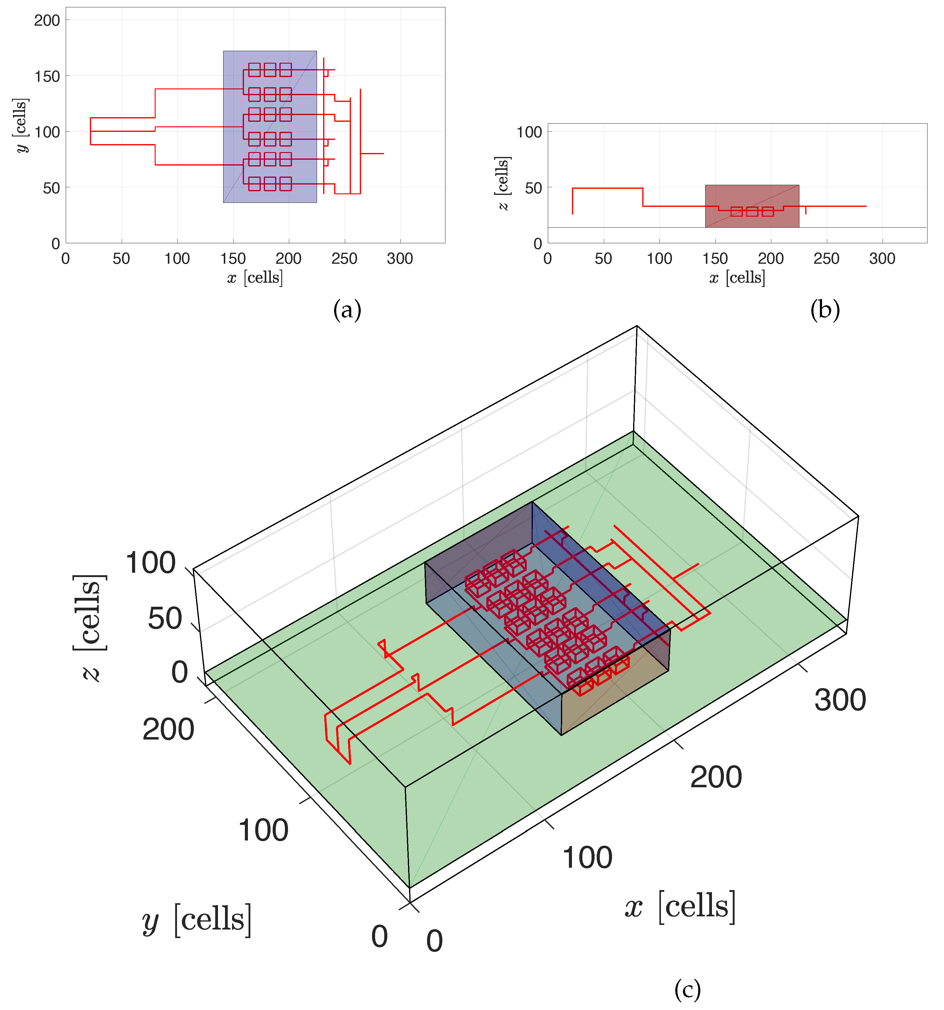
Figure 2.
Log magnitude of the electric field measured inside and outside the valve hall. (a) 2 m segments of the conductors that nominally pass through the valve hall walls are removed. (b) The conductors that pass through the walls are intact.
Figure 2.
Log magnitude of the electric field measured inside and outside the valve hall. (a) 2 m segments of the conductors that nominally pass through the valve hall walls are removed. (b) The conductors that pass through the walls are intact.
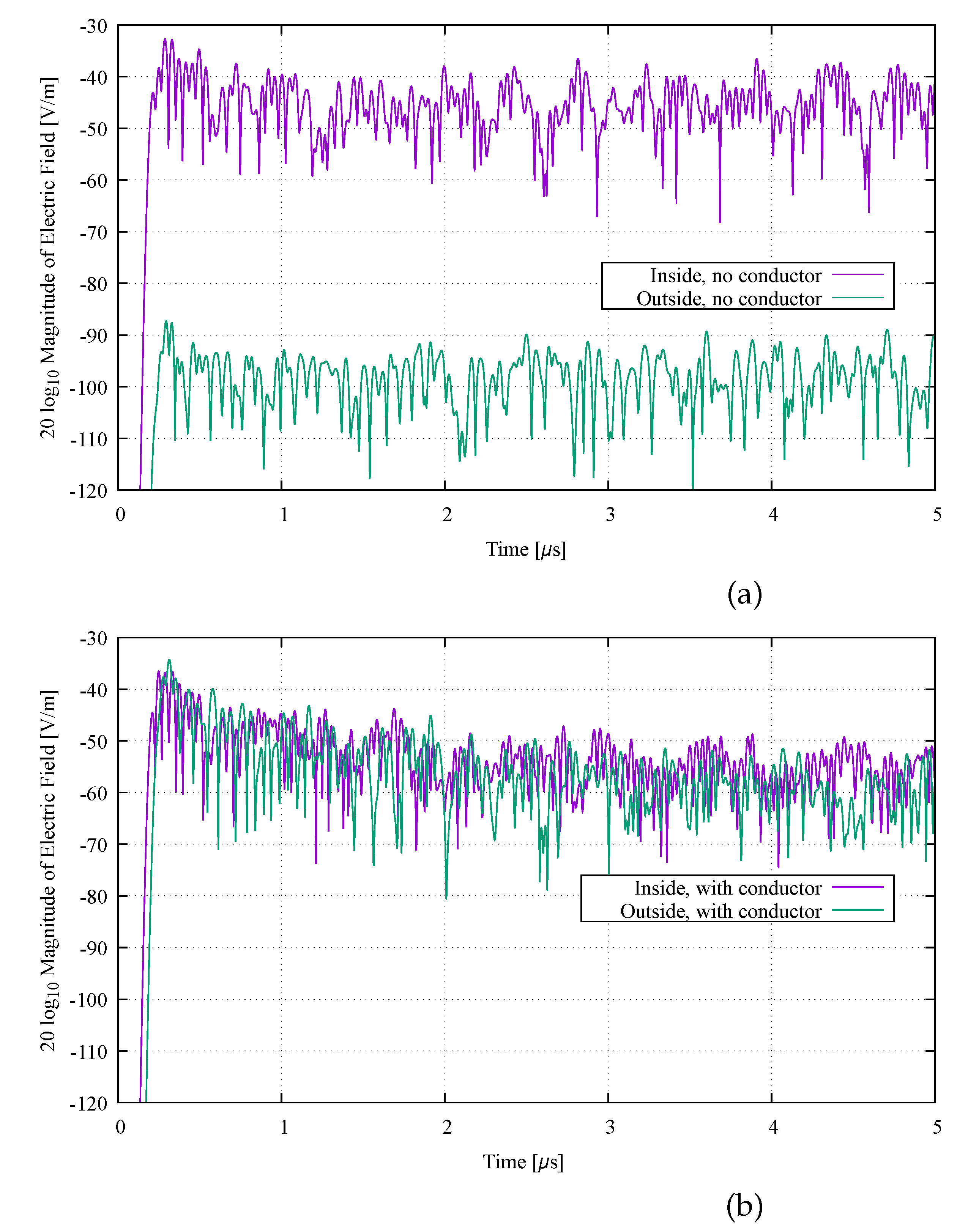
Figure 3.
Log magnitude of the spectral content of the component of the field measured at two points. (a) The observation points are inside and outside the valve hall. The reference curve shows the Fourier transform of the source function. (b) Fields at the observations points normalized by the source function. (c) The valve hall has been removed with no other changes to the simulation.
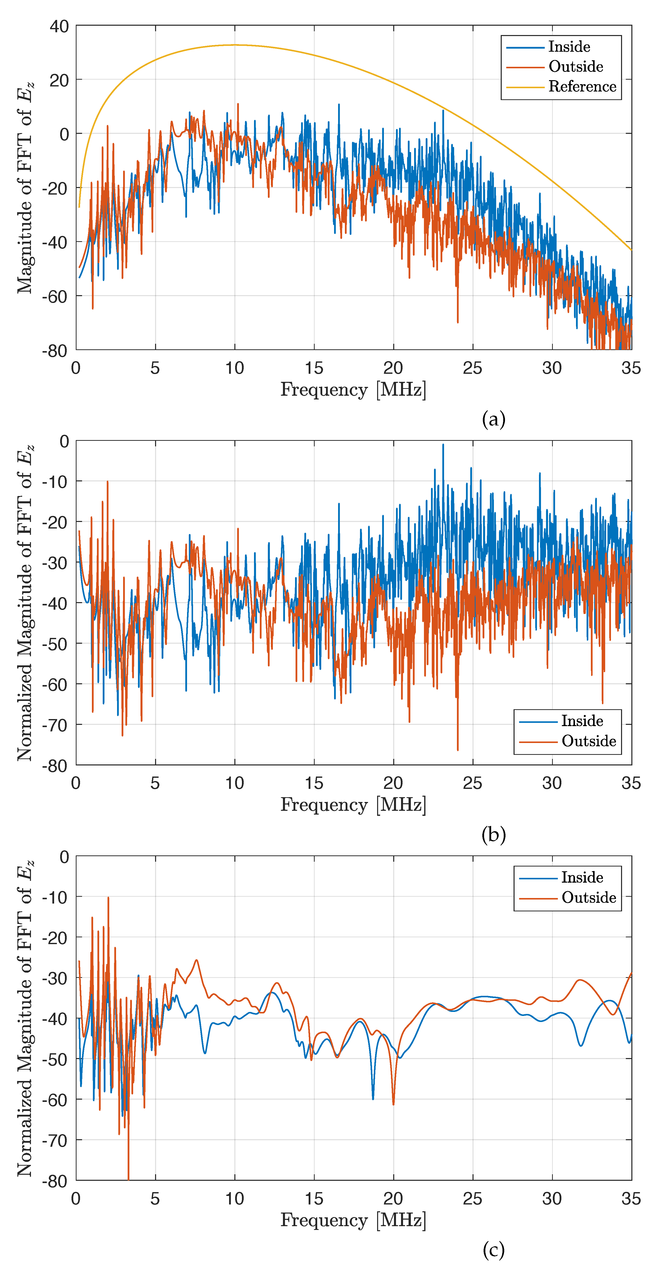
Figure 4.
Log magnitude of the normalized spectrum of the current measured at two points along the top-most line from the valve hall to the DC hall. (a) The hall is present. (b) The hall has been removed.
Figure 4.
Log magnitude of the normalized spectrum of the current measured at two points along the top-most line from the valve hall to the DC hall. (a) The hall is present. (b) The hall has been removed.
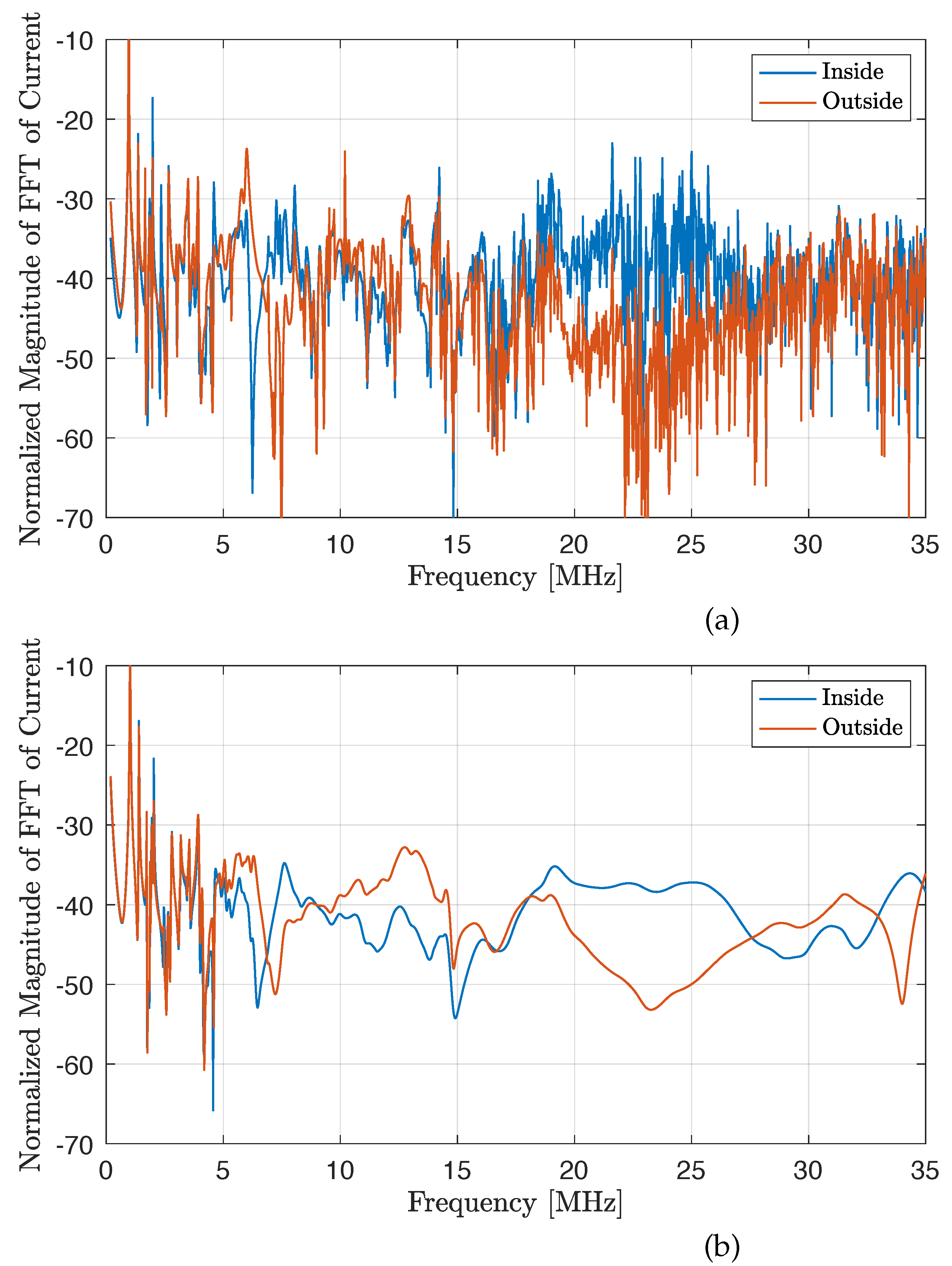
Figure 5.
Electric field magnitude measured approximately 200 m from the converter station (a) Field observed when the valve hall is and is not present. (b) Field observed when there is and is not a lossy dielectric slab placed in the valve hall.
Figure 5.
Electric field magnitude measured approximately 200 m from the converter station (a) Field observed when the valve hall is and is not present. (b) Field observed when there is and is not a lossy dielectric slab placed in the valve hall.
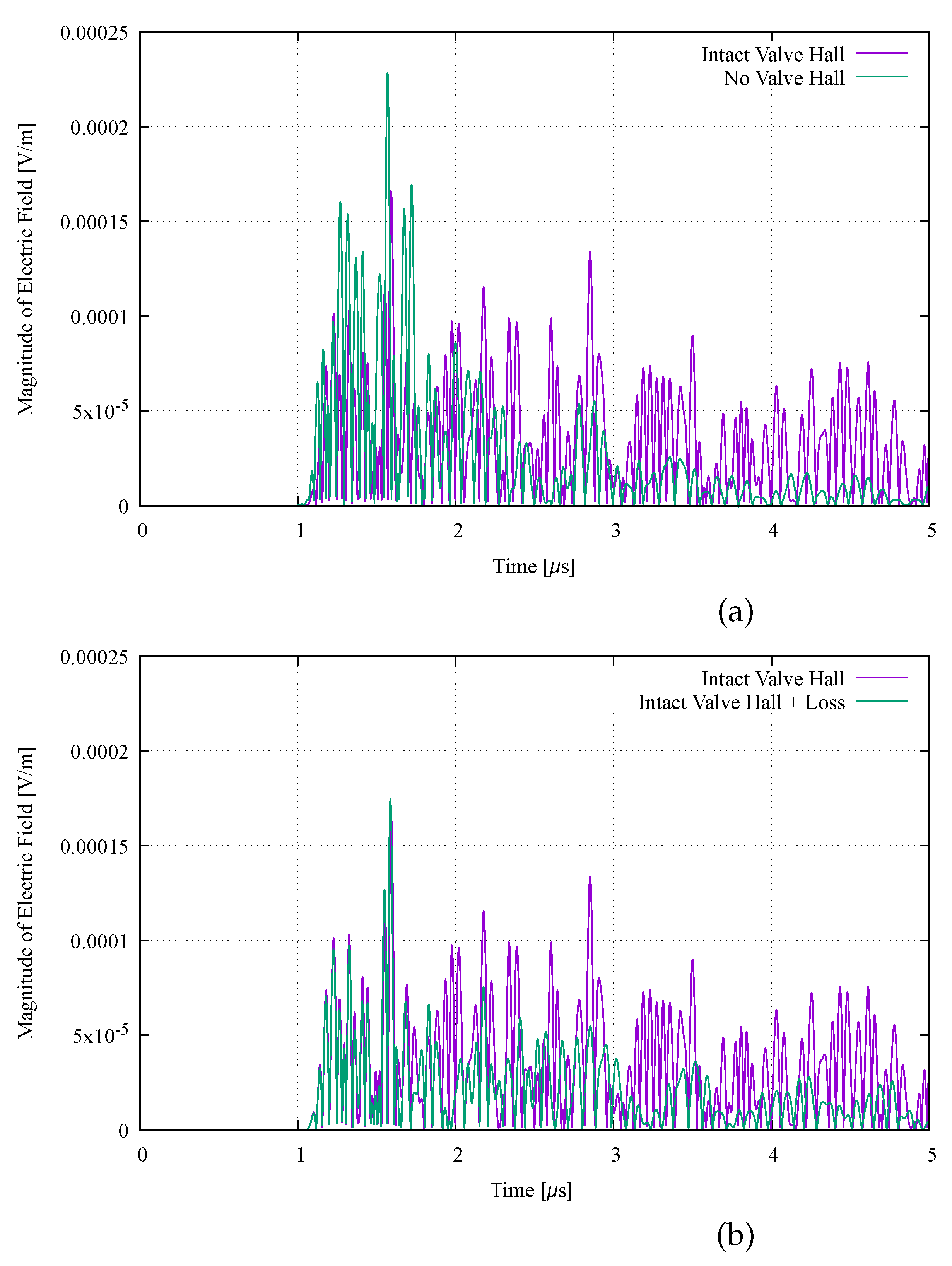
Figure 6.
Normalized spectrum of the field (in dB) measured approximately 200 m from the valve hall. Results are shown for an intact valve hall, when no valve hall is present, and when the valve hall is intact but contains a lossy dielectric slab.
Figure 6.
Normalized spectrum of the field (in dB) measured approximately 200 m from the valve hall. Results are shown for an intact valve hall, when no valve hall is present, and when the valve hall is intact but contains a lossy dielectric slab.
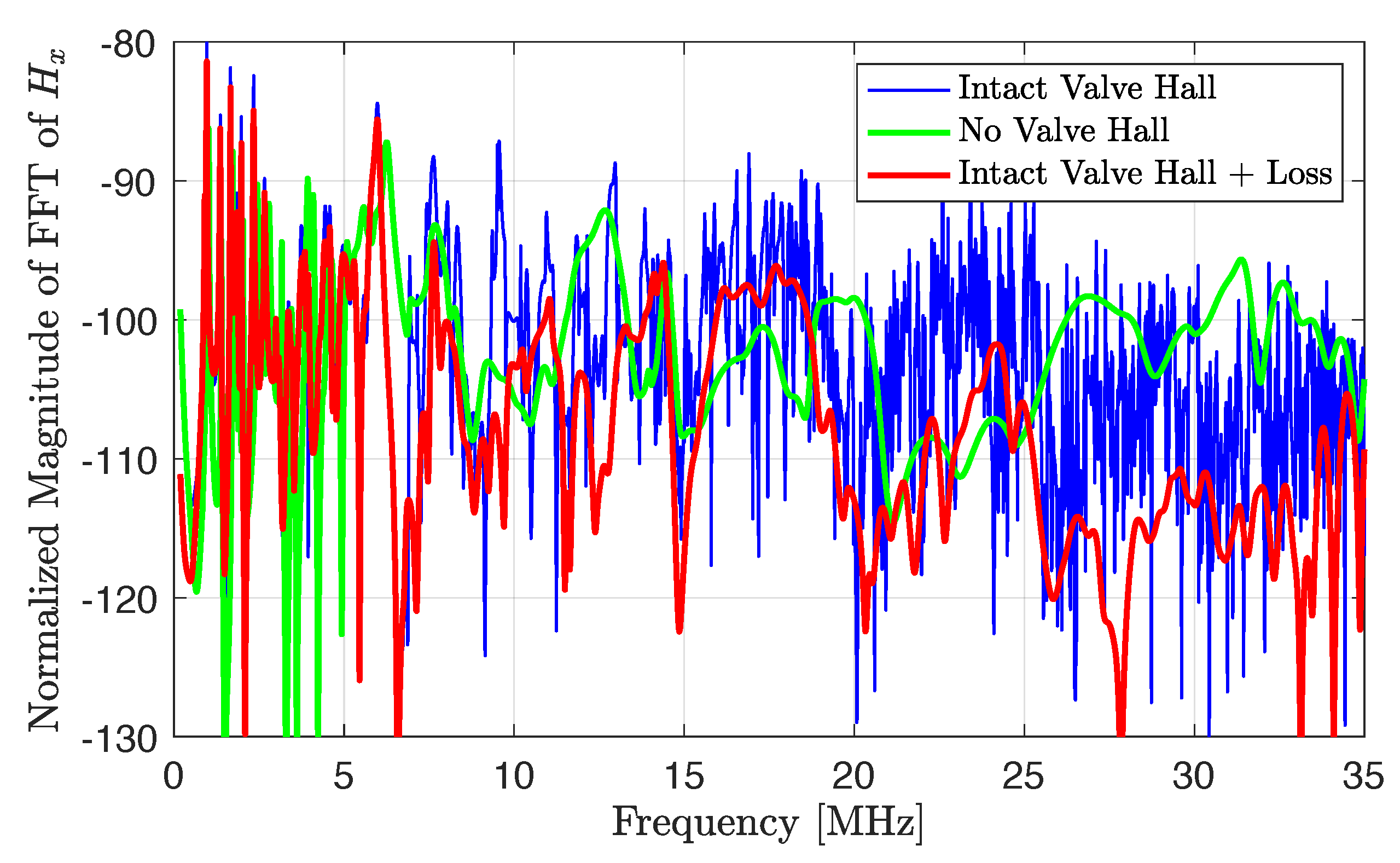

Table 1.
Shielding effectiveness of a “perfect” valve hall as determined by NEC-5. The measurement point was 200 m from the center of the m cubic hall.
Table 1.
Shielding effectiveness of a “perfect” valve hall as determined by NEC-5. The measurement point was 200 m from the center of the m cubic hall.
| Frequency | Change Causedby Valve Hall |
|---|---|
| 200 kHz | dB |
| 1 MHz | dB |
| 5 MHz | dB |
| 25 MHz | dB |
Disclaimer/Publisher’s Note: The statements, opinions and data contained in all publications are solely those of the individual author(s) and contributor(s) and not of MDPI and/or the editor(s). MDPI and/or the editor(s) disclaim responsibility for any injury to people or property resulting from any ideas, methods, instructions or products referred to in the content. |
© 2024 by the authors. Licensee MDPI, Basel, Switzerland. This article is an open access article distributed under the terms and conditions of the Creative Commons Attribution (CC BY) license (http://creativecommons.org/licenses/by/4.0/).
Copyright: This open access article is published under a Creative Commons CC BY 4.0 license, which permit the free download, distribution, and reuse, provided that the author and preprint are cited in any reuse.


