
Submitted:
09 July 2024
Posted:
11 July 2024
You are already at the latest version
Abstract
Due to the optical properties of the Electron Transport Layer (ETL) and Hole Transport Layer (HTL), inverted perovskite solar cells can perform better than traditional perovskite solar cells. It is essential to compare both types to understand their efficiencies. In this article, we studied inverted perovskite solar cells with NiOx/CH3NH3Pb3/ETL (ETL = MoO3, TiO2, ZnO) structures. Our results showed that the optimal thickness of NiOx is 80 nm for all structures. The optimal perovskite thickness is 600 nm for solar cells with ZnO and MoO3, and 800 nm for those with TiO2. For the ETLs, the best thicknesses are 100 nm for ZnO, 80 nm for MoO3, and 60 nm for TiO2. We found that the efficiencies of inverted perovskite solar cells with ZnO, MoO3, and TiO2 as ETLs, and with optimal layer thicknesses, are 30.16%, 18.69%, and 35.21%, respectively. These efficiencies are 1.5%, 5.7%, and 1.5% higher than those of traditional perovskite solar cells. Our study highlights the potential of optimizing layer thicknesses in inverted perovskite solar cells to achieve higher efficiencies than traditional structures.
Keywords:
perovskite
; inverted structure
; thickness
; metal oxides
; photoelectric parameters.
1. Introduction
Today, the demand for energy is increasing rapidly. To meet the growing need for electrical energy while preserving the environment and resources, we must turn to renewable energy sources. Among these, wind and solar energy are particularly popular. Solar cells are used to convert solar energy into electrical energy. Currently, there are four generations of solar cells, each aiming to address the limitations of the previous generation. Solar cells have three main types of losses: optical [1], electrical [2], and thermal [3]. Optical losses include reflection, spectral mismatch [4], parasitic absorption [5], and transmission. To reduce reflection, textures [6] and antireflection coatings [7] are applied. Depending on the refractive index of the antireflection coating, the reflection coefficient can be reduced by more than 20%. Spectral mismatch occurs because solar cells primarily absorb photons with energy higher than the material's band gap. High-energy photons generate hot carriers, which are unstable and recombine quickly through a process called thermalization, leading to parasitic absorption and heating of the solar cell. Due to spectral mismatch and parasitic absorption, the efficiency of single-junction solar cells cannot exceed 33%, according to the Shockley-Queisser limit [8]. Tandem [9] and heterojunction structures [10] offer solutions to spectral mismatch, with theoretical efficiencies of up to 68% achievable using tandem cells with an infinite number of stacked cells [11]. Another way to improve efficiency of solar cells is inclusion of metal nanoparticles to use from nanoplasmonic effect [12].
In the industry, silicon solar cells are predominantly produced. However, in the last 15 years, there has been growing interest in perovskite solar cells. Perovskite materials possess unique properties that make them excellent candidates for photovoltaic devices, such as tunable band gaps by mixing cations and anions [13], shallow traps [14], long diffusion lengths [15], and high absorption [16] in thin layers. Despite their potential, perovskite solar cells are not yet widely manufactured due to their low stability [17] and size effect [18]. The main causes of degradation in perovskite solar cells are structural distortion [19] under temperature and illumination, as well as ion migration [20]. Various methods have been proposed to improve their stability.
The architecture of a perovskite solar cell consists of an electron transport layer (ETL), light-absorbing layers (perovskite), and a hole transport layer (HTL). In our previous work [21], we studied a ZnO/perovskite/NiOx structure and found that the optical properties of NiOx might be superior to ZnO, serving both as an antireflection coating and a charge transport layer. In this study, we decided to investigate an inverted perovskite solar cell with an HTL/perovskite/ETL structure. We used NiOx as the HTL and ZnO, MoO3, and TiO2 as the ETL. According to the band structure of perovskite solar cells (as shown in Figure 1), ZnO, MoO3, and TiO2 are excellent choices for the ETL because they do not block electrons. In thin layers, the thickness of each layer significantly affects the performance of the solar cell [22]. Therefore, we focused on optimizing each layer of the inverted perovskite solar cell and identifying the optimal material for the ETL. Additionally, we compared inverted and traditional perovskite solar cells to determine which configuration performs better.
2. Materials and Methods
There are three primary methods employed in solar cell research: theoretical analysis, experimental investigation, and numerical simulation. Over the years, simulation techniques have seen significant advancements and gained popularity. Among the various simulation tools used for solar cell research—Silvaco TCAD, Sentaurus TCAD, SCAPS-1D, and Comsol Multiphysics—Sentaurus TCAD stands out due to its extensive range of physical models and its capability to perform both 2D and 3D simulations [23]. In this study, Sentaurus TCAD was selected for its versatility in handling complex physical models. We utilized four main tools within Sentaurus TCAD: Sentaurus Structure Editor, Sentaurus Device, Sentaurus Visual, and Sentaurus Workbench. Sentaurus Visual was particularly instrumental for visualizing results and importing data, while Sentaurus Workbench facilitated integration of various simulation components. The geometric model of the solar cell was constructed using Sentaurus Structure Editor. Figure 2 illustrates the geometric structure of the solar cell, highlighting variables such as the thickness of the electron transport layer (ETL), hole transport layer (HTL), and perovskite layers, which were adjusted within a specified range. Additionally, the doping concentrations and types of these layers (HTL, ETL, and perovskite) were defined within Sentaurus Structure Editor, set respectively at 1e16 cm-3, 1e17 cm-3, and 1e18 cm-3. In numerical simulations, the mesh size significantly influences result reliability. Our structure was meshed using two different sizes: a smaller mesh size of 1 nm for active regions such as heterojunctions, and a larger mesh size of 2 nm for other regions.
After creating the geometric model, the next step is to define the physical properties of each material used in the solar cell through numerical simulation in Sentaurus Device. Sentaurus Device allows us to control physical models, simulation accuracy, light intensity, temperature, and contacts. Choosing the right physical models from the options in Sentaurus TCAD is crucial, as using inappropriate ones can lead to unexpected errors in the simulation process. Simulating solar cells typically involves two stages: optical and electrical simulation. In optical simulation, we calculate important factors like photogenerated electron-hole pairs, how much light is absorbed, and how much is reflected or transmitted. There are three main optical models: Transfer Matrix Method (TMM), Ray Tracing, and Beam Propagation. Each model has its advantages; for example, TMM is good for including interference effects in thin layers [24], while Ray Tracing is useful for textured solar cells because it tracks how light rays move through them [25]. In our study of planar solar cells, where we're focusing on varying the thickness of each layer, we chose to use TMM (as defined by formula 1) for optical simulation. This model was chosen because it accurately includes interference effects, which is important for understanding how changing layer thickness affects solar cell performance.
Here: M is the matrix, Ei is the electrical field of incident light, Er is the electric field of reflected light and Et is the electric field of transmitted light.
In solar cells, ions, electrons, and holes play key roles in generating an electric field. The electrical field and potential within the solar cell are determined by solving the Poisson equation, represented by formula 2. This equation takes into account the distribution of electrons and holes using the Fermi distribution to calculate their concentrations.
Here: ε is the permittivity, ND and NA are the concentrations of donor and acceptor, q is the charge.
Electrons and holes in solar cells are separated by the internal electric field created by ions, after which they begin to migrate towards the electrodes. Various models exist to describe the transport of these charge carriers, such as Drift-Diffusion, thermodynamic, and hydrodynamic models. The thermodynamic and hydrodynamic models account for the influence of temperature on charge carrier transport. However, in our study, we did not specifically investigate the temperature effects on solar cell performance. Therefore, we employed the drift-diffusion model [26], as expressed by formula 3, to calculate charge carrier transport.
Here: µn, µp are the mobilities of electron and holes, Fn, Fp are the electron and hole quasi-Fermi potentials, Pn, Pp are the thermoelectric power of electrons and holes, T is the absolute temperature.
Photogenerated electrons and holes in solar cells can recombine through various mechanisms, such as defects within the material or by emitting photons. There are three main types of recombination: radiative recombination, Shockley-Read-Hall recombination, and Auger recombination. These mechanisms are all considered in our simulation to accurately model the behavior of charge carriers. Additionally, as an electrical boundary condition, the ohmic boundary condition [27] described by formula 4 is utilized. This condition helps define how the electrical potential behaves at the boundaries of the solar cell structure, ensuring consistency and accuracy in our simulations.
Here: ni,eff is concentration of effective intrinsic carrier, φF is Fermi potential of contact.
3. Results and discussion
3.1. Optimization of ETL
We studied the NiOx/perovskite/MeO structure (MeO = TiO2, ZnO, MoO3) to optimize geometrical sizes. The thicknesses of the NiOx and perovskite layers were set at 100 nm and 200 nm, respectively, while the ETL layer thickness varied from 20 nm to 200 nm. We calculated photoelectric parameters for each thickness. Figure 3 shows the dependence of short circuit current (a) and output power (b) on the ETL layer thickness. Both parameters exhibited a peak value within the 20-200 nm range. When comparing ETL layers, ZnO had the highest short circuit current, while TiO2 had the lowest. In experiment, it was found that perovskite solar cell with ZnO as ETL has higher short circuit current [28]. However, in terms of output power, TiO2 demonstrated the highest value, and MoO3 had the lowest. Notably, the output power of solar cells with ZnO and TiO2 was nearly the same, but it was significantly lower in case of MoO3. This discrepancy between output power and short circuit current is unusual, as high short circuit current typically correlates with better output power. The reason for TiO2's superior output power, despite its lower short circuit current, may be attributed to its higher fill factor and efficient charge extraction properties, which offset the lower current generated.
To further investigate this inconsistency, we examined the dependence of the fill factor on ETL layer thickness, as shown in Figure 4. The fill factor did not change significantly with thickness variations: the amplitude of change for MoO3 was less than 0.1%, for TiO2 less than 0.01%, and for ZnO less than 0.08%. Among all ETL layers, the solar cell with TiO2 exhibited the highest fill factor, while the one with MoO3 had the lowest. This high fill factor in the TiO2 layer is crucial, as it allows the solar cell to achieve maximum output power despite having the lowest short circuit current. The stability of the fill factor across different thicknesses further emphasizes the robustness of TiO2 as an effective ETL material in this structure. The high fill factor of TiO2 can be attributed to its excellent electronic properties, such as high electron mobility and favorable energy level alignment with the perovskite layer, which reduces recombination losses and improves charge collection efficiency. In experiment, Wang also found [29] that TiO2 ETL enhances the extraction and transportation of electrons to contacts from perovskite. So, our simulation results agree with experiment. On the other hand, the low fill factor of MoO3 might be due to its lower electron mobility and potential issues with charge recombination at the interface, leading to less efficient charge extraction.
Based on the analysis, the optimal thicknesses of the ETL layers for maximum output power were identified: 80 nm for MoO3, 60 nm for TiO2, and 100 nm for ZnO. Table 1 provides the photoelectric parameters of solar cells with various ETL layers at these optimal thicknesses. The short circuit current for ZnO, MoO3, and TiO2 layers at optimal thicknesses was 15.79 mA/cm², 15.62 mA/cm², and 15.52 mA/cm², respectively. The open circuit voltage was approximately 1.2 V for all ETLs. The fill factor was 54.18% for MoO3, 84.47% for TiO2, and 82.15% for ZnO. Consistent with our previous studies, TiO2 demonstrated a superior fill factor compared to other ETL materials. The efficiency of solar cells with optimal ETL layer thicknesses was 16.04% for MoO3, 25.61% for TiO2, and 24.6% for ZnO. These results confirm that TiO2 is the best ETL layer for the inverted perovskite structure, combining a high fill factor and efficiency, making it an excellent choice for optimizing solar cell performance.
3.2. Optimization of HTL
After finding the optimal thickness of ETL layers for each material, we decided to determine the optimal thickness of HTL layers. In this case, we maintained the optimal thickness of ETL layers and varied the NiOx layer thickness from 20 nm to 200 nm. Figure 5 presents the dependence of short circuit current (a) and output power (b) on NiOx layer thickness. Again, the short circuit current of the solar cell with ZnO as the ETL layer is the highest, and the lowest belongs to TiO2 as the ETL layer. However, the output power of the solar cell with TiO2 as the ETL layer is the highest, while the lowest belongs to MoO3. Both short circuit current and output power functions depending on NiOx layer thickness have an extremum in the range of 20-200 nm, indicating that the optimal value of the HTL layer thickness lies within this range. The increase and subsequent decrease in performance with varying thickness are due to the balance between photogeneration and recombination. Increasing the ETL or HTL layer thickness helps capture more photons but also leads to increased recombination. Therefore, ETL and HTL layers should be thick enough to transmit electrons or holes with a lower recombination rate to the contacts. According to the output power, the optimum value of the HTL layers is 80 nm for all three solar cells, suggesting that the type of ETL layer does not affect the optimal value of the HTL layer, likely because the sun rays fall from the HTL layer side. In experiment [30], it was predicted that optimal thickness of NiOx is between 50-150 nm. Experimental optimal thickness range includes our optimal thickness obtained by simulation and it shows agreement of our results with experiment.
The thickness of the HTL layer can affect the resistivity of the solar cell. As the ETL or HTL layer thickness increases, so does the resistivity, which in turn affects the fill factor of the solar cell. Figure 6 shows the dependence of the fill factor on the thickness of the HTL layer. Unlike the ETL layer thickness, the fill factor changed significantly with changes in HTL layer thickness. The amplitude of fill factor fluctuation was 0.7% for MoO3, 1.4% for TiO2, and 0.7% for ZnO. The solar cell with TiO2 had the highest fill factor, while the lowest belonged to MoO3. This explains why the output power of the TiO2-based solar cell is the highest, even though its short circuit current is the lowest. The fill factor significantly determines the optimal material for the ETL layer in our study. The functional dependence of the fill factor of the solar cell with TiO2 as the ETL layer on HTL layer thickness had an extremum in the range of 20-200 nm, consistent with short circuit current and output power. The quality of the curve for the functional dependence of the fill factor on HTL layer thickness for solar cells with ZnO and MoO3 was similar but with lower fluctuation amplitude, indicating that they did not significantly affect the optimal value of HTL layer thickness where output power reaches maximum value.
We provided the photoelectric parameters of solar cells with optimal ETL and HTL layer thicknesses in Table 2. The optimal thicknesses of ETL layers with MoO3, TiO2, ZnO, and HTL with NiOx are 80 nm, 60 nm, 100 nm, and 80 nm, respectively. The short circuit current of solar cells with optimal ETL and HTL layer thicknesses is 15.92 mA/cm² for MoO3, 15.84 mA/cm² for TiO2, and 16.06 mA/cm² for ZnO. The optimization of the HTL layer did not affect the open circuit voltage. The efficiency of solar cells with MoO3, TiO2, and ZnO is 16.35%, 26.15%, and 25.03%, respectively, with fill factors of 54.17%, 87.5%, and 82.21%, respectively. Both the fill factor and efficiency of the solar cell with MoO3 are 1.6 times lower than those of the solar cell with TiO2. The resistivity of TiO2 [31], MoO3 [32], and ZnO [33] varies with thickness, with average values of 1 Ωcm, 5.4 Ωcm, and 2 Ω*cm, respectively. Because of high resistivity of MoO3, its efficiency and fill factor is the lowest.
3.3. Optimization of Perovskite layer
After optimizing the HTL layer thickness, we observed efficiency increases of 0.31%, 0.54%, and 0.43% for MoO3, TiO2, and ZnO, respectively. Despite these improvements, the efficiency gains were lower than expected by optimizing only the ETL and HTL layers. Therefore, we decided to optimize the perovskite layer as well. We varied the thickness of the perovskite layer from 200 nm to 1600 nm while keeping the optimal ETL and HTL layer thicknesses from previous calculations. Figure 7 shows the dependence of short circuit current (a) and output power (b) on perovskite layer thickness. The short circuit current increased with the perovskite layer thickness and saturated after 1200 nm. This saturation occurs due to the balance between photogeneration and recombination rates. As the perovskite layer thickness increases, both absorbed photon density and recombination increase. Initially, the short circuit current of the solar cell with TiO2 was the lowest, but after increasing the thickness, it became the highest. The short circuit current increased from 15.8 mA/cm² to 22.6 mA/cm² when the perovskite layer thickness was increased from 200 nm to 1600 nm. The output power of each solar cell showed a maximum at a specific perovskite layer thickness. For the solar cell with MoO3, the output power increased from 10.4 mW/cm² to 11.8 mW/cm² when the perovskite layer thickness increased from 200 nm to 600 nm, after which it began to decrease. The output power of the solar cell with ZnO also increased from 15.8 mW/cm² to 19.1 mW/cm² within the perovskite layer thickness range of 200-600 nm. The output power of the solar cell with TiO2 behaved differently; it increased from 16.5 mW/cm² to 22.3 mW/cm² in the range of 200-800 nm and then began to saturate, showing little change beyond 800 nm. Based on these observations, we identified the optimal perovskite layer thickness for solar cells with MoO3, ZnO, and TiO2 as 600 nm, 600 nm, and 800 nm, respectively. For the solar cells with MoO3 and ZnO, the optimal perovskite thickness corresponded to the point of maximum output power. For the solar cell with TiO2, the optimal thickness was determined at the point where the output power started to saturate.
In Figure 8, the dependence of the fill factor on perovskite layer thickness is shown. As the thickness of the perovskite layer increases from 200 nm to 1600 nm, the fill factor of solar cells with MoO3, TiO2, and ZnO decreased by 14.4%, 1.9%, and 13.8%, respectively. Increasing the thickness of the perovskite layer leads to more photon absorption but also increases the recombination rate. The optimal thickness is determined by balancing recombination and photogeneration. The fill factor of solar cells with ZnO and MoO3 decreased significantly, which is the main reason for having an exact optimal thickness of the perovskite layer where the maximum output power is reached. On the other hand, the fill factor of the solar cell with TiO2 decreased only slightly, leading to the saturation of output power rather than a distinct maximum as the perovskite layer thickness increased. This suggests that TiO2 is the best ETL for inverted perovskite solar cells. The slight decrease in the fill factor for the solar cell with TiO2 indicates better charge transport and lower fill factor compared to ZnO and MoO3.
Each layer of the inverted perovskite solar cell has been fully optimized. In Table 3, the photoelectric parameters of the solar cells with optimal ETL, HTL, and perovskite layers are provided. There is no significant difference in the short circuit currents among the solar cells. The short circuit currents for solar cells with MoO3, TiO2, and ZnO are 21.12 mA/cm², 21.83 mA/cm², and 21.2 mA/cm², respectively. Before optimizing the perovskite layer thickness, the short circuit current of the solar cell with TiO2 was the lowest; after optimization, it became the highest. Due to the increased thickness of the perovskite layer, the open circuit voltage decreased by 0.012 V. The fill factors for solar cells with MoO3, TiO2, and ZnO are 44.14%, 86.83%, and 75.78%, respectively. The fill factor of the solar cell with TiO2 is almost twice that of the solar cell with MoO3. Consequently, the efficiencies of solar cells with MoO3, TiO2, and ZnO are 18.69%, 35.21%, and 30.16%, respectively. Similar to the fill factor, the efficiency of the solar cell with TiO2 is twice that of the solar cell with MoO3. Azri’s simulation study [34] also revealed that ZnO and TiO2 are the best candidates for ETL. ETL layers primarily transport electrons, and the band offset of conduction bands between the perovskite and ETL plays a vital role. The band offsets for MoO3, TiO2, and ZnO with the perovskite are 2.7 eV, 0.3 eV, and 0.6 eV, respectively. The large band offset for MoO3 could be the main reason for the low fill factor of the solar cell with MoO3. The optimization process highlights the critical importance of selecting and tuning the ETL, HTL, and perovskite layers to maximize the performance of inverted perovskite solar cells. Despite the initial lower short circuit current, the solar cell with TiO2 demonstrated the highest overall efficiency and fill factor, underscoring its superiority as an ETL material. The significant differences in band offsets among the materials suggest that minimizing the band offset between the perovskite and ETL is crucial for achieving higher fill factors and efficiencies.
3.3. Comparision of Traditional and Inverted Perovskite Solar Cells
Our main mission was to determine the better structure for perovskite solar cells, whether inverted or traditional. In Table 4, we present the photoelectric parameters of traditional solar cells with the same thicknesses of ETL, HTL, and perovskite layers as those in the inverted structure. We compared the photoelectric parameters of traditional and inverted perovskite solar cells. The short circuit currents of traditional solar cells with MoO3, TiO2, and ZnO are 1.9 mA/cm², 3.5 mA/cm², and 1.2 mA/cm² smaller than those of inverted solar cells. This indicates that the solar cell with ZnO has the highest short circuit current among the traditional configurations. This difference can be explained by the optical properties of the materials used. While the open circuit voltage of traditional solar cells is also smaller, the fill factor is greater compared to inverted solar cells. The efficiency of traditional solar cells with MoO3, TiO2, and ZnO are 1.5%, 5.7%, and 1.5% lower than those of the inverted solar cells. NiOx based inverted perovskite solar cell achieved more than 20% efficiency in experiment and it was higher than that of traditional one. These results suggest that the inverted structure generally provides better performance in terms of short circuit current and efficiency, despite the traditional structure showing a higher fill factor. This comprehensive comparison highlights the advantages of the inverted configuration in maximizing the overall efficiency and photoelectric performance of perovskite solar cells.
When we change the illumination side, it significantly affects the optical properties of the solar cells. The differences in efficiency and short circuit current between inverted and traditional perovskite solar cells can be attributed to these optical properties. In Figure 9, we present the absorption and reflection spectra of both inverted and traditional perovskite solar cells. In the wavelength range of 0.5-0.8 µm, the absorption coefficient of the inverted solar cell with TiO2 is higher than that of the other solar cells. This higher absorption is due to a lower reflection coefficient in this range. The improved absorption and reflection properties of the inverted solar cell with TiO2 contribute to its higher efficiency. The enhanced optical properties, combined with better electronic properties, explain why the inverted structure with TiO2 performs better in terms of efficiency and short circuit current.
In the case of traditional perovskite solar cells, the absorption coefficient of the solar cell with TiO2 is smaller than that of other solar cells. Additionally, its reflection coefficient is higher. In traditional solar cells, the optical properties of ETL layers play a crucial role in determining the absorption and reflection coefficients. In Figure 10, we present the real (a) and imaginary (b) parts of the complex refractive indices of ZnO, TiO2, MoO3, NiOx, and perovskite. The average refractive indices of ZnO, TiO2, MoO3, NiOx, and perovskite are 1.9, 1.92, 2.2, 1.65, and 2.62, respectively. Given that the refractive index of air is 1, the theoretical optimal refractive index for a layer between air and perovskite should be 1.61. Therefore, based on refractive indices, NiOx is the best candidate. In an inverted perovskite solar cell, light falls on solar cell from the NiOx side. In this configuration, NiOx acts as an effective antireflection coating in addition to its role in hole transport. Besides, in experiment, Wu found [35] that good device lifetime of inverted perovskite solar cell with NiOx as HTL can be stable up to 50 days.
The refractive indices of ETL materials are higher than the optimal refractive index for antireflection purposes. As a result, the absorption coefficient of the traditional solar cell is smaller than that of the inverted solar cell. The maximum absorption coefficients of inverted and traditional perovskite solar cells in the wavelength range of 0.3-0.9 µm are 1 and 0.85, respectively. Therefore, the efficiency of the inverted solar cell is higher than that of the traditional solar cell due to the higher absorption coefficient.
4. Conclusions
In conclusion, our study investigated the performance of inverted perovskite solar cells by optimizing the thickness of their layers. We focused on three materials for the electron transport layer (ETL) - ZnO, MoO3, and TiO2 - and found that TiO2 provided the best results. The performance was evaluated based on short circuit current, output power, and fill factor. TiO2 showed the highest efficiency and fill factor, making it the best choice for the ETL. The study also examined the hole transport layer (HTL) and the perovskite layer. We found that the optimal thickness for the HTL was 80 nm for all tested ETL materials, while the optimal thickness for the perovskite layer varied: 600 nm for MoO3 and ZnO, and 800 nm for TiO2. After optimizing these layers, the solar cell with TiO2 as the ETL achieved the highest efficiency of 35.21%, significantly outperforming the cells with ZnO and MoO3. This shows the importance of selecting and fine-tuning the materials and thicknesses of each layer to maximize the performance of perovskite solar cells. Our findings highlight that TiO2 is the most effective ETL material due to its excellent electronic properties and alignment with the perovskite layer, which enhances charge collection and reduces recombination losses. This optimization is crucial for improving the efficiency and stability of perovskite solar cells, making them more viable for large-scale energy production.
Supplementary Materials
The following supporting information can be downloaded at the website of this paper posted on Preprints.org., Figure S1: title; Table S1: title; Video S1: title.
Author Contributions
I.G.: conceptualization, investigation, methodology, writing-original draft, validation, software, project administration; O.A.: methodology, investigation, data curation, writing—review and editing, funding acquisition, formal analysis, validation; R.A.: conceptualization, investigation, methodology, validation, supervision; Z.A.B.: visualization, re-sources, funding acquisition, validation, writing—review and editing; V.A.: validation, formal analysis, software, writing—review and editing. All authors have read and agreed to the published version of the manuscript.
Funding
This research received no external funding.
Data Availability Statement
Data will be made available upon request from the corresponding author.
Acknowledgments
The authors would like to express their gratitude to Jasurbek Gulomov for his valuable feedback on the draft and for the insightful discussions regarding the obtained results.
Conflicts of Interest
The authors declare no conflicts of interest.
References
- Shen, X.; Jiang, S.; Wang, X.; Zhou, H.; Yu, Z. Suppressing Optical Losses in Solar Cells via Multifunctional and Large-Scale Geometric Arrays. Nanomaterials 2023, 13, 2766. [Google Scholar] [CrossRef] [PubMed]
- Saeed, F.; Haseeb Khan, M.; Tauqeer, H.A.; Haroon, A.; Idrees, A.; Shehrazi, S.M.; Prokop, L.; Blazek, V.; Misak, S.; Ullah, N. Numerical Investigation of Photo-Generated Carrier Recombination Dynamics on the Device Characteristics for the Perovskite/Carbon Nitride Absorber-Layer Solar Cell. Nanomaterials 2022, 12, 4012. [Google Scholar] [CrossRef] [PubMed]
- Vaillon, R.; Dupré, O.; Cal, R.B.; Calaf, M. Pathways for Mitigating Thermal Losses in Solar Photovoltaics. Scientific Reports 2018, 8, 1–9. [Google Scholar] [CrossRef]
- Gulomov, J.; Accouche, O.; Al Barakeh, Z.; Aliev, R.; Gulomova, I.; Neji, B. Atom-to-Device Simulation of MoO3/Si Heterojunction Solar Cell. Nanomaterials 2022, 12, 4240. [Google Scholar] [CrossRef]
- Fell, A.; Greulich, J.; Feldmann, F.; Messmer, C.; Schön, J.; Bivour, M.; Schubert, M.C.; Glunz, S.W. Modeling Parasitic Absorption in Silicon Solar Cells with a Near-Surface Absorption Parameter. Solar Energy Materials and Solar Cells 2022, 236, 111534. [Google Scholar] [CrossRef]
- Gulomov, J.; Aliev, R. Analyzing Periodical Textured Silicon Solar Cells by the TCAD Modeling. Scientific and Technical Journal of Information Technologies, Mechanics and Optics 2021, 21, 626–632. [Google Scholar] [CrossRef]
- Zhao, J.; Green, M.A. Optimized Antireflection Coatings for High-Efficiency Silicon Solar Cells. IEEE Trans Electron Devices 1991, 38, 1925–1934. [Google Scholar] [CrossRef]
- Ehrler, B.; Alarcón-Lladó, E.; Tabernig, S.W.; Veeken, T.; Garnett, E.C.; Polman, A. Photovoltaics Reaching for the Shockley-Queisser Limit. ACS Energy Lett 2020, 5, 3029–3033. [Google Scholar] [CrossRef]
- Lal, N.N.; Dkhissi, Y.; Li, W.; Hou, Q.; Cheng, Y.B.; Bach, U. Perovskite Tandem Solar Cells. Adv Energy Mater 2017, 7, 1602761. [Google Scholar] [CrossRef]
- Gulomov, J.; Accouche, O.; Aliev, R.; Azab, M.; Gulomova, I. Analyzing the ZnO and CH3NH3PbI3 as Emitter Layer for Silicon Based Heterojunction Solar Cells. Computers, Materials & Continua 2022, 74, 575–590. [Google Scholar] [CrossRef]
- Iftiquar, S.M.; Jung, J.; Yi, J.; De Vos, A. Detailed Balance Limit of the Efficiency of Tandem Solar Cells. J Phys D Appl Phys 1980, 13, 839. [Google Scholar] [CrossRef]
- Gulomov, J.; Accouche, O. Gold Nanoparticles Introduced ZnO/Perovskite/ Silicon Heterojunction Solar Cell. IEEE Access 2022, 10, 119558–119565. [Google Scholar] [CrossRef]
- Liu, Y.; Li, B.; Xu, J.; Yao, J. Improvement of Thermal Stability and Photoelectric Performance of Cs2PbI2Cl2/CsPbI2.5Br0.5 Perovskite Solar Cells by Triple-Layer Inorganic Hole Transport Materials. Nanomaterials 2024, 14, 742. [Google Scholar] [CrossRef] [PubMed]
- Baumann, A.; Väth, S.; Rieder, P.; Heiber, M.C.; Tvingstedt, K.; Dyakonov, V. Identification of Trap States in Perovskite Solar Cells. Journal of Physical Chemistry Letters 2015, 6, 2350–2354. [Google Scholar] [CrossRef] [PubMed]
- Stranks, S.D.; Eperon, G.E.; Grancini, G.; Menelaou, C.; Alcocer, M.J.P.; Leijtens, T.; Herz, L.M.; Petrozza, A.; Snaith, H.J. Electron-Hole Diffusion Lengths Exceeding 1 Micrometer in an Organometal Trihalide Perovskite Absorber. Science (1979) 2013, 342, 341–344. [Google Scholar] [CrossRef] [PubMed]
- Tao, H.; Zhang, W.; Zhang, C.; Han, L.; Wang, J.; Tan, B.; Li, Y.; Kan, C. High Absorption Perovskite Solar Cell with Optical Coupling Structure. Opt Commun 2019, 443, 262–267. [Google Scholar] [CrossRef]
- Singh, A.N.; Jana, A.; Selvaraj, M.; Assiri, M.A.; Yun, S.; Nam, K.W. Achieving Order in Disorder: Stabilizing Red Light-Emitting α-Phase Formamidinium Lead Iodide. Nanomaterials 2023, 13, 3049. [Google Scholar] [CrossRef]
- Zhang, Y.; Zhao, Z.; Liu, Z.; Tang, A. The Scale Effects of Organometal Halide Perovskites. Nanomaterials 2023, 13, 2935. [Google Scholar] [CrossRef] [PubMed]
- Straus, D.B.; Guo, S.; Abeykoon, A.M.; Cava, R.J. Understanding the Instability of the Halide Perovskite CsPbI3 through Temperature-Dependent Structural Analysis. Advanced Materials 2020, 32, 2001069. [Google Scholar] [CrossRef]
- Yuan, Y.; Huang, J. Ion Migration in Organometal Trihalide Perovskite and Its Impact on Photovoltaic Efficiency and Stability. Acc Chem Res 2016, 49, 286–293. [Google Scholar] [CrossRef]
- Gulomov, J.; Accouche, O.; Aliev, R.; Neji, B.; Ghandour, R.; Gulomova, I.; Azab, M. Geometric Optimization of Perovskite Solar Cells with Metal Oxide Charge Transport Layers. Nanomaterials 2022, 12, 2692. [Google Scholar] [CrossRef] [PubMed]
- Lee, D.; Kim, K.H.; Kim, H.D. Thickness Optimization of Charge Transport Layers on Perovskite Solar Cells for Aerospace Applications. Nanomaterials 2023, 13, 1848. [Google Scholar] [CrossRef] [PubMed]
- Gulomov, J.; Accouche, O.; Aliev, R.; Ghandour, R.; Gulomova, I. Investigation of N-ZnO/p-Si and n-TiO2/p-Si Heterojunction Solar Cells: TCAD + DFT. IEEE Access 2023, 11, 38970–38981. [Google Scholar] [CrossRef]
- Sachchidanand; Kumar, A.; Sharma, P. Transfer Matrix Method-Based Efficiency Enhancement of Lead-Free Cs3Sb2Br9 Perovskite Solar Cell. Solar Energy 2023, 259, 63–71. [CrossRef]
- Gulomov, J.; Aliev, R.; Urmanov, B. Effect of the Thickness on Photoelectric Parameters of a Textured Silicon Solar Cell. Journal of Surface Investigation 2022, 16, 416–420. [Google Scholar] [CrossRef]
- Lin, A.S.; Phillips, J.D. Drift-Diffusion Modeling for Impurity Photovoltaic Devices. IEEE Trans Electron Devices 2009, 56, 3168–3174. [Google Scholar] [CrossRef]
- Miller, W.A.; Olsen, L.C. Model Calculations for Silicon Inversion Layer Solar Cells. Solar Cells 1983, 8, 371–395. [Google Scholar] [CrossRef]
- Baltakesmez, A.; Biber, M.; Tüzemen, S. Inverted Planar Perovskite Solar Cells Based on Al Doped ZnO Substrate. J Radiat Res Appl Sci 2018, 11, 124–129. [Google Scholar] [CrossRef]
- Wang, Y.; Wan, J.; Ding, J.; Hu, J.S.; Wang, D. A Rutile TiO2 Electron Transport Layer for the Enhancement of Charge Collection for Efficient Perovskite Solar Cells. Angewandte Chemie International Edition 2019, 58, 9414–9418. [Google Scholar] [CrossRef]
- Wang, T.; Ding, D.; Zheng, H.; Wang, X.; Wang, J.; Liu, H.; Shen, W. Efficient Inverted Planar Perovskite Solar Cells Using Ultraviolet/Ozone-Treated NiOx as the Hole Transport Layer. Solar RRL 2019, 3, 1900045. [Google Scholar] [CrossRef]
- Saini, K.K.; Sharma, S.D.; Chanderkant; Kar, M.; Singh, D.; Sharma, C.P. Structural and Optical Properties of TiO2 Thin Films Derived by Sol–Gel Dip Coating Process. J Non Cryst Solids 2007, 353, 2469–2473. [Google Scholar] [CrossRef]
- Meng, L.; Yamada, A. Low-Resistance Orthorhombic MoO3-x Thin Film Derived by Two-Step Annealing. Thin Solid Films 2018, 665, 179–183. [Google Scholar] [CrossRef]
- Raimondi, D.L.; Kay, E. High Resistivity Transparent ZnO Thin Films. Journal of Vacuum Science and Technology 1970, 7, 96–99. [Google Scholar] [CrossRef]
- Azri, F.; Meftah, A.; Sengouga, N.; Meftah, A. Electron and Hole Transport Layers Optimization by Numerical Simulation of a Perovskite Solar Cell. Solar Energy 2019, 181, 372–378. [Google Scholar] [CrossRef]
- Wu, Y.W.; Wang, C.Y.; Yang, S.H. Exploration and Optimization of the Polymer-Modified NiOx Hole Transport Layer for Fabricating Inverted Perovskite Solar Cells. Nanomaterials 2024, 14, 1054. [Google Scholar] [CrossRef]
Figure 1.
Band structure of NiOx/CH3NH3PbI3/TiO2 (a), NiOx/CH3NH3PbI3/ZnO (b) va NiOx/CH3NH3PbI3/MoO3 (c) solar cells.
Figure 1.
Band structure of NiOx/CH3NH3PbI3/TiO2 (a), NiOx/CH3NH3PbI3/ZnO (b) va NiOx/CH3NH3PbI3/MoO3 (c) solar cells.
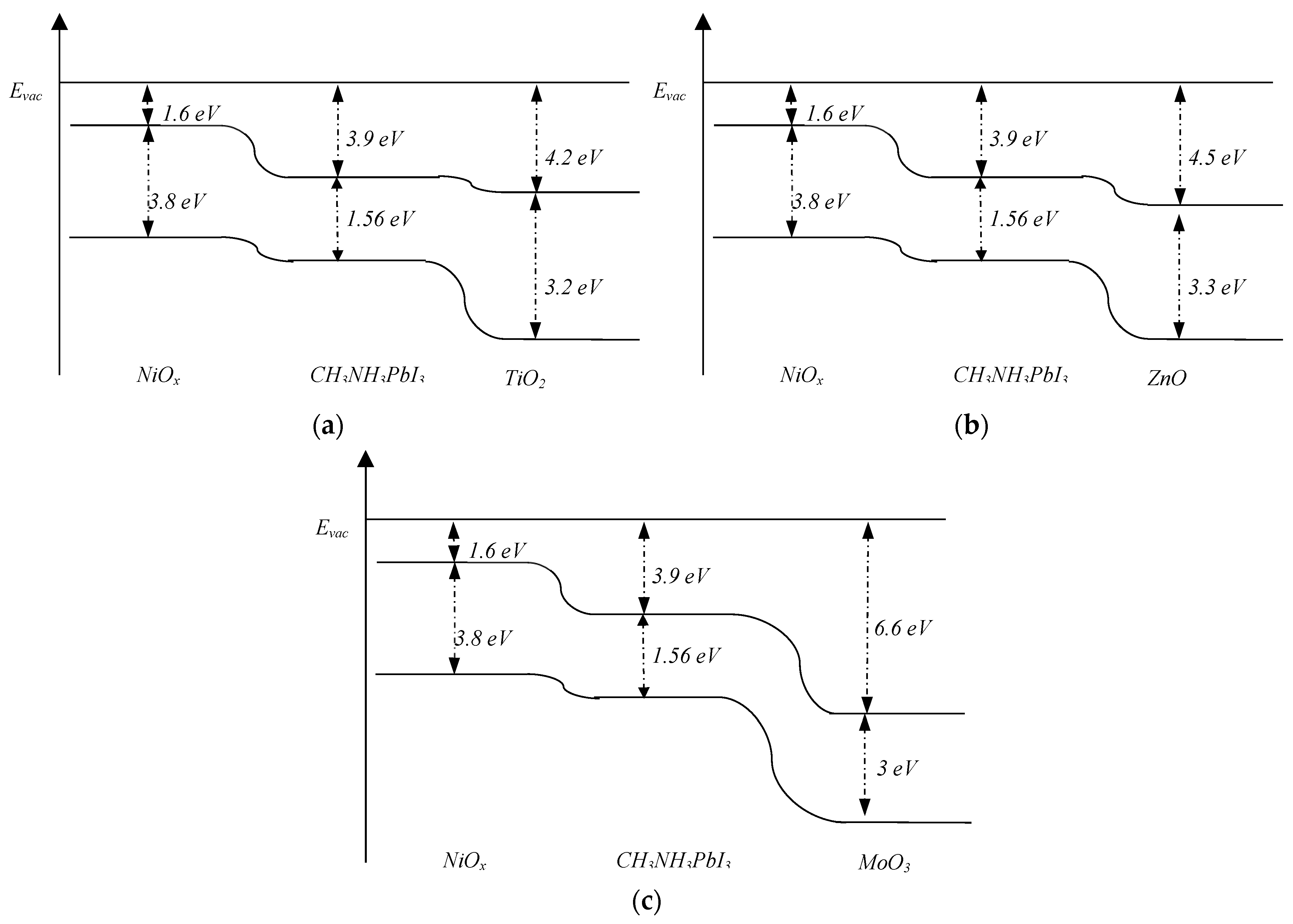
Figure 2.
Geometrical structure of inverted perovskite solar cell. Lk – width of contact region, dHTL – thickness of HTL, dp – Thickness of perovskite layer, dETL – thickness of ETL, L – width of solar cell..
Figure 2.
Geometrical structure of inverted perovskite solar cell. Lk – width of contact region, dHTL – thickness of HTL, dp – Thickness of perovskite layer, dETL – thickness of ETL, L – width of solar cell..
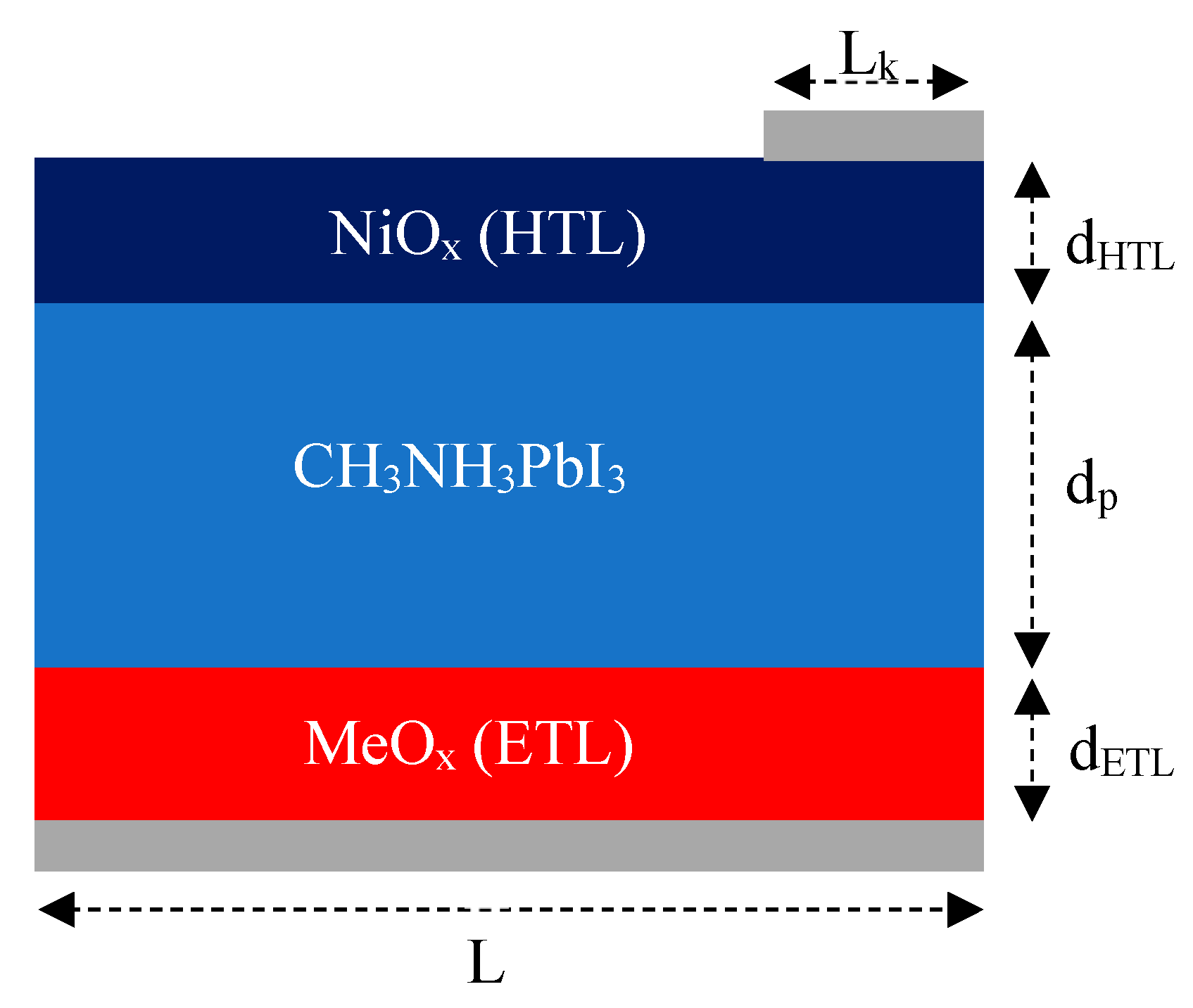
Figure 3.
Dependence of short circuit current (a) and output power (b) on thickness of ETL.
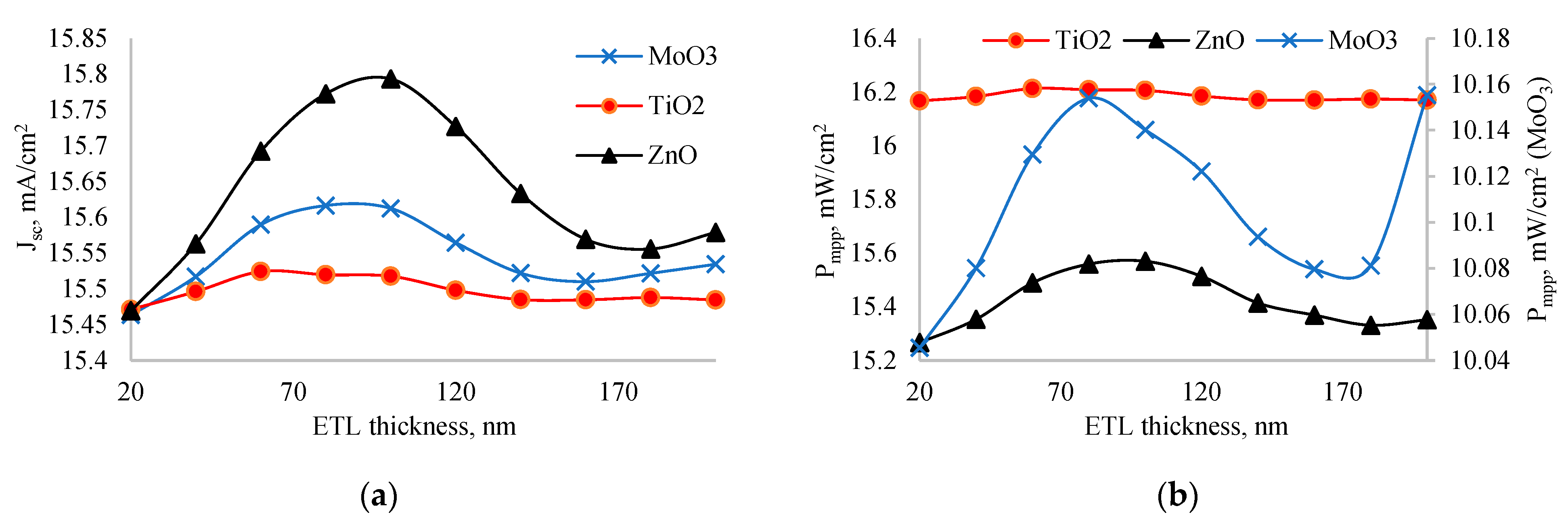
Figure 4.
Dependence of fill factor of solar cells with MoO3, TiO2 and ZnO as ETL on thickness of ETL.
Figure 4.
Dependence of fill factor of solar cells with MoO3, TiO2 and ZnO as ETL on thickness of ETL.
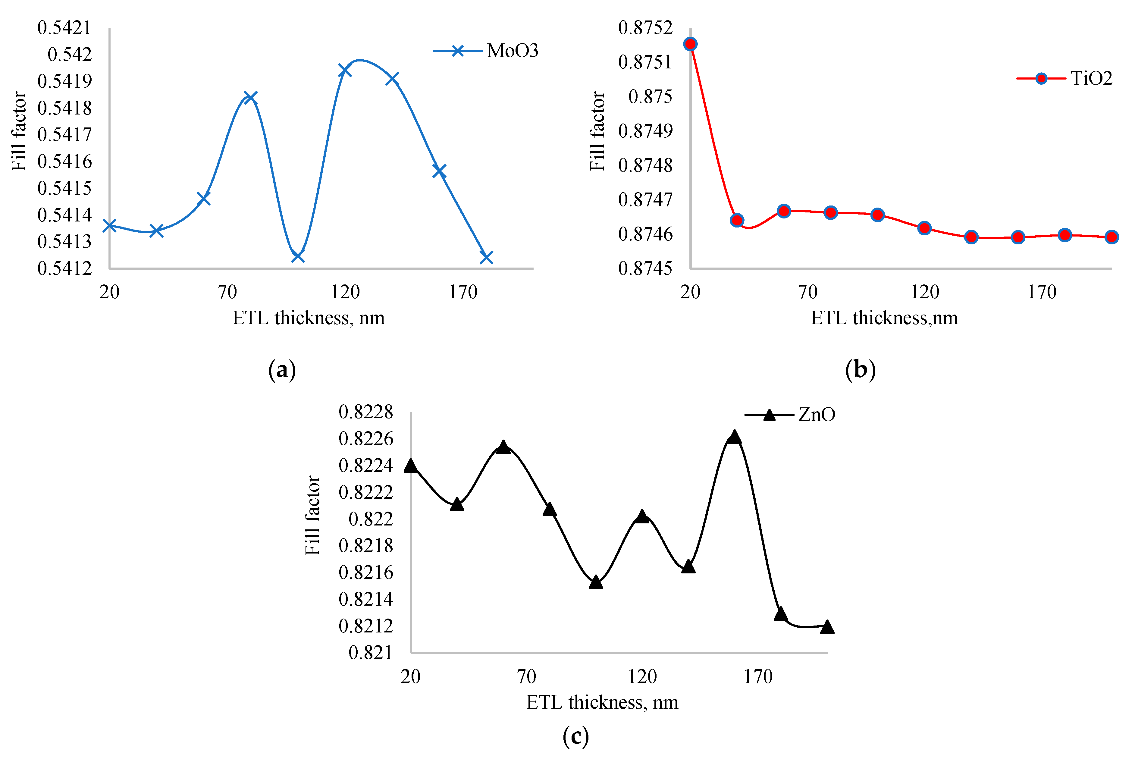
Figure 5.
Dependence of short circuit current (a) and output power (b) on thickness of HTL.
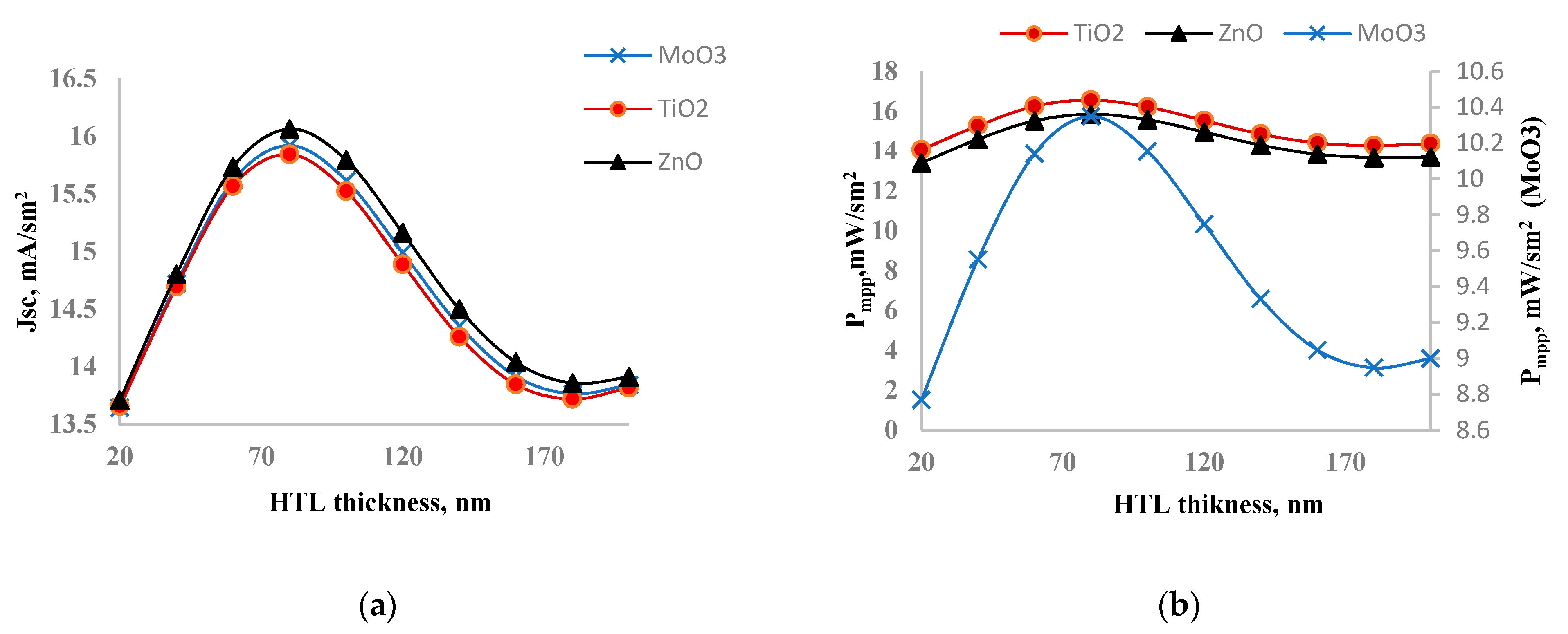
Figure 6.
Dependence of fill factor of solar cells with MoO3, TiO2 and ZnO as ETL on thickness of HTL.
Figure 6.
Dependence of fill factor of solar cells with MoO3, TiO2 and ZnO as ETL on thickness of HTL.
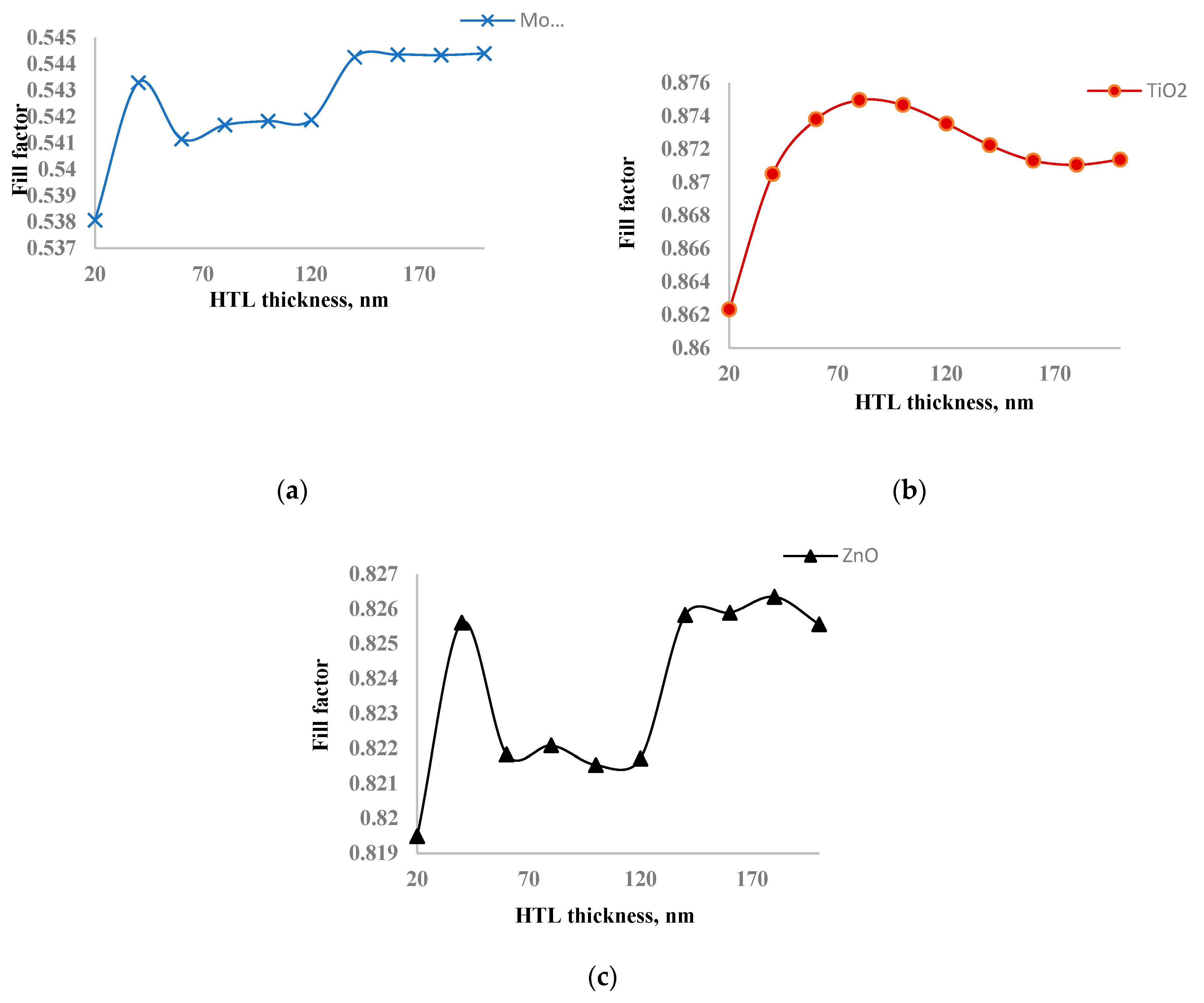
Figure 7.
Dependence of short circuit current (a) and output power (b) on thickness of perovskite layer thickness.
Figure 7.
Dependence of short circuit current (a) and output power (b) on thickness of perovskite layer thickness.
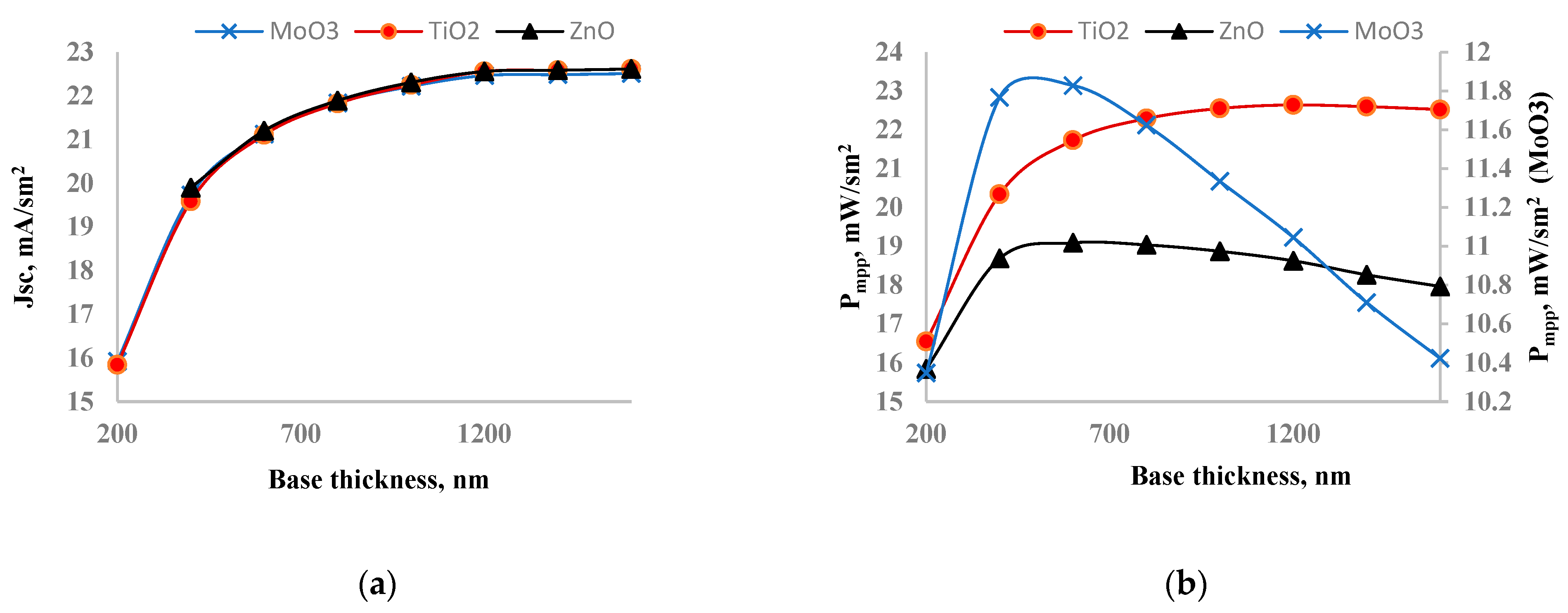
Figure 8.
Dependence of fill factor of solar cells with MoO3, TiO2 and ZnO as ETL on thickness of perovskite layer.
Figure 8.
Dependence of fill factor of solar cells with MoO3, TiO2 and ZnO as ETL on thickness of perovskite layer.
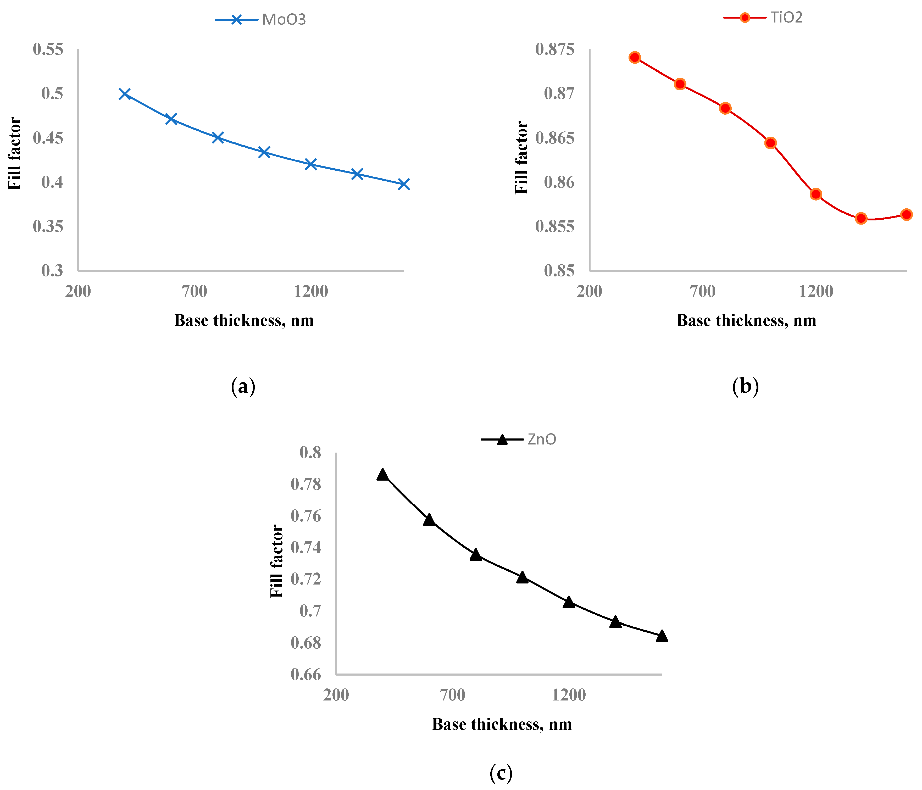
Figure 9.
Absorption (a,c) and reflection (b,d) spectrum of inverted (a,b) and traditional (c,d) perovskite solar cells.
Figure 9.
Absorption (a,c) and reflection (b,d) spectrum of inverted (a,b) and traditional (c,d) perovskite solar cells.
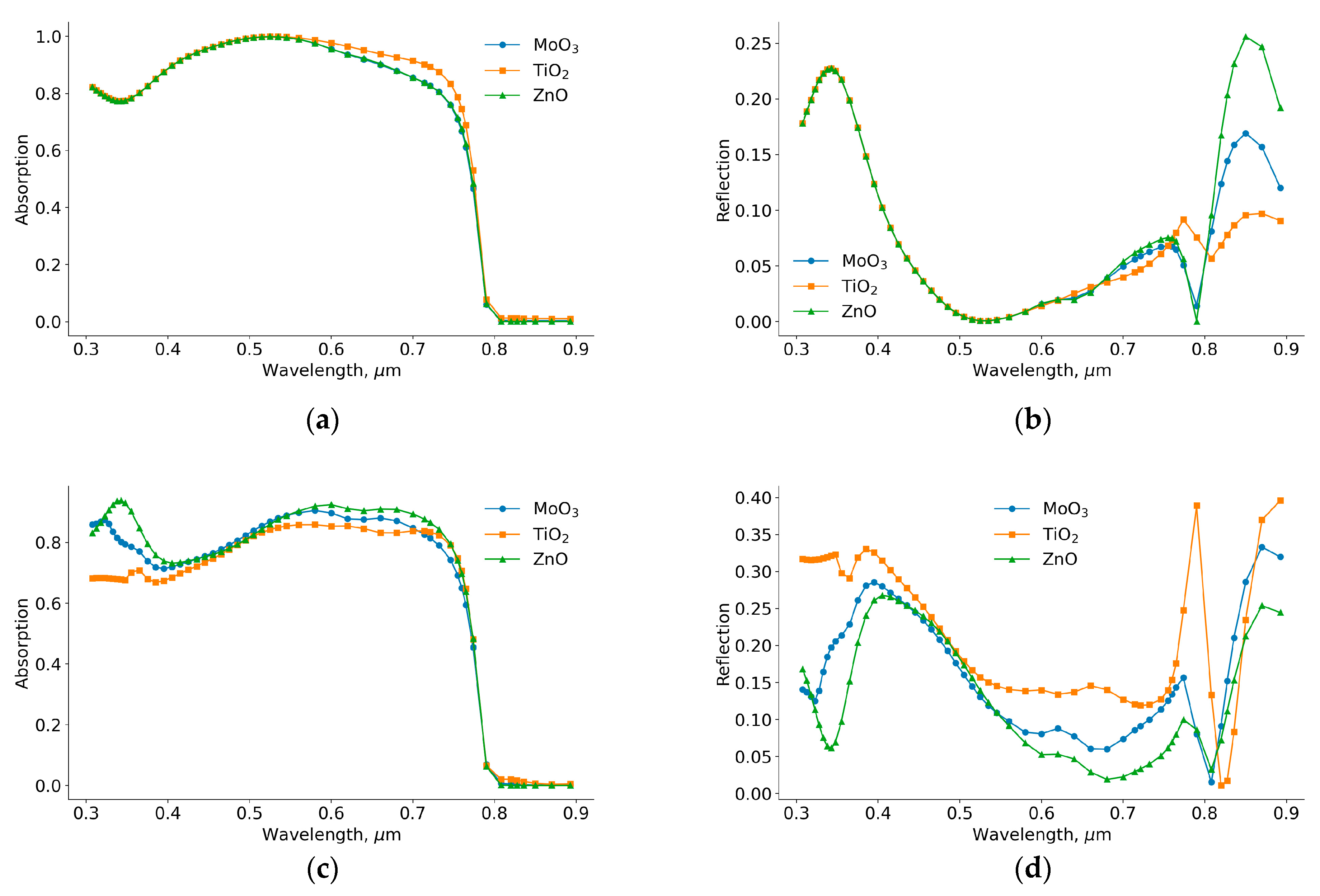
Figure 10.
Dependence of short circuit current (a) and output power (b) on thickness of perovskite layer thickness.
Figure 10.
Dependence of short circuit current (a) and output power (b) on thickness of perovskite layer thickness.
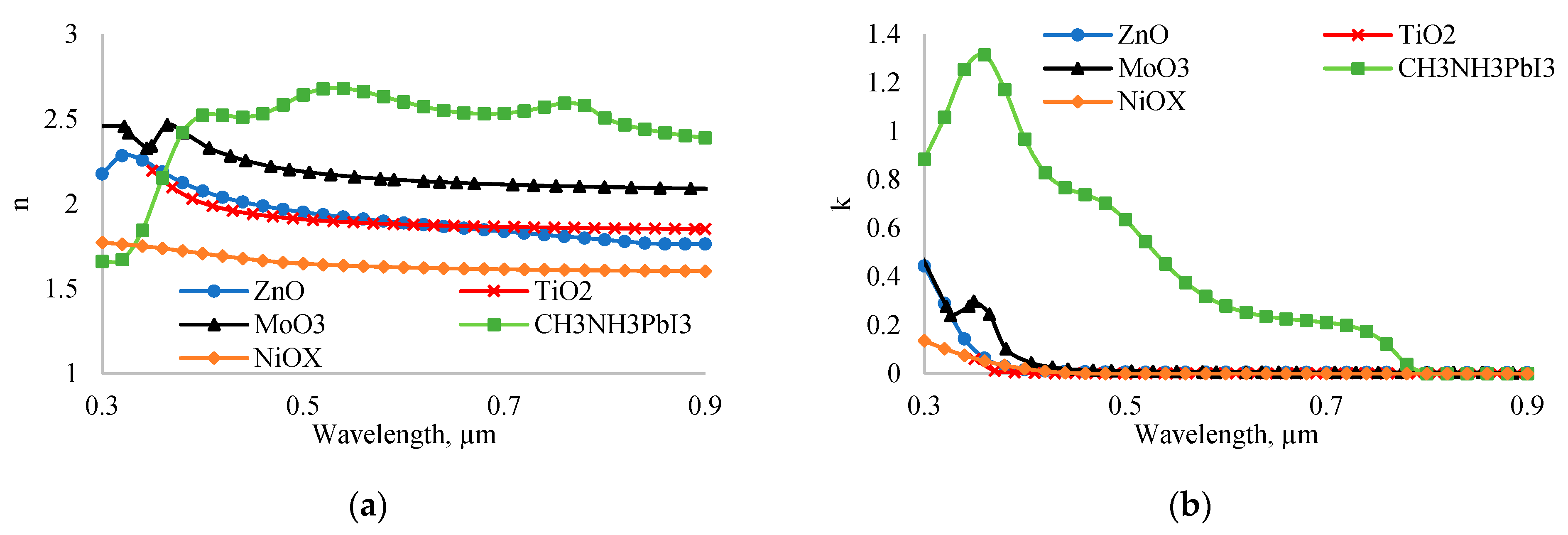

Table 1.
Photoelectric parameters of inverted perovskite solar cell with optimal ETL thikcness. dbase=200 nm and dHTL=100 nm.
Table 1.
Photoelectric parameters of inverted perovskite solar cell with optimal ETL thikcness. dbase=200 nm and dHTL=100 nm.
| Materials | dETL, nm |
Jsc, mA/cm2 | Uoc, V | Pmpp, mW/cm2 |
FF, % | η, % |
|---|---|---|---|---|---|---|
| MoO3 | 80 | 15.62 | 1.200 | 10.15 | 54.18 | 16.04 |
| TiO2 | 60 | 15.52 | 1.194 | 16.21 | 87.47 | 25.61 |
| ZnO | 100 | 15.79 | 1.200 | 15.57 | 82.15 | 24.60 |
Table 2.
Photoelectric parameters of inverted perovskite solar cell with optimal ETL and HTL thicknesses. dbase=200 nm.
Table 2.
Photoelectric parameters of inverted perovskite solar cell with optimal ETL and HTL thicknesses. dbase=200 nm.
| Materials | dETL, nm | dHTL, nm | JSC, mA/sm2 | UOC, V | Pmpp, mW/sm2 | FF, % | ɳ, % |
|---|---|---|---|---|---|---|---|
| MoO3 | 80 | 80 | 15.92 | 1.200 | 10.35 | 54.17 | 16.35 |
| TiO2 | 60 | 80 | 15.84 | 1.194 | 16.55 | 87.50 | 26.15 |
| ZnO | 100 | 80 | 16.06 | 1.200 | 15.84 | 82.21 | 25.03 |
Table 3.
Photoelectric parameters of inverted perovskite solar cell with optimal ETL, HTL and perovskite layer thicknesses.
Table 3.
Photoelectric parameters of inverted perovskite solar cell with optimal ETL, HTL and perovskite layer thicknesses.
| Materials | dBASE, nm | dETL, nm | dHTL, nm | JSC, mA/sm2 | UOC, V | Pmpp, mW/sm2 | FF, % | ɳ, % |
|---|---|---|---|---|---|---|---|---|
| MoO3 | 600 | 80 | 80 | 21.12 | 1.188 | 11.83 | 47.14 | 18.69 |
| TiO2 | 800 | 60 | 80 | 21.83 | 1.176 | 22.29 | 86.83 | 35.21 |
| ZnO | 600 | 100 | 80 | 21.20 | 1.188 | 19.09 | 75.78 | 30.16 |
Table 4.
Photoelectric parameters of traditional perovskite solar cell with optimal ETL and HTL thicknesses.
Table 4.
Photoelectric parameters of traditional perovskite solar cell with optimal ETL and HTL thicknesses.
| Materials | dBASE, nm | dETL, nm | dHTL, nm | JSC, mA/sm2 | UOC, V | Pmpp, mW/sm2 | FF, % | ɳ, % |
|---|---|---|---|---|---|---|---|---|
| MoO3 | 600 | 80 | 80 | 19.20 | 1.182 | 10.86 | 47.85 | 17.15 |
| TiO2 | 800 | 60 | 80 | 18.30 | 1.171 | 18.68 | 87.14 | 29.51 |
| ZnO | 600 | 100 | 80 | 20.01 | 1.182 | 18.16 | 76.81 | 28.69 |
Disclaimer/Publisher’s Note: The statements, opinions and data contained in all publications are solely those of the individual author(s) and contributor(s) and not of MDPI and/or the editor(s). MDPI and/or the editor(s) disclaim responsibility for any injury to people or property resulting from any ideas, methods, instructions or products referred to in the content. |
© 2024 by the authors. Licensee MDPI, Basel, Switzerland. This article is an open access article distributed under the terms and conditions of the Creative Commons Attribution (CC BY) license (http://creativecommons.org/licenses/by/4.0/).
Copyright: This open access article is published under a Creative Commons CC BY 4.0 license, which permit the free download, distribution, and reuse, provided that the author and preprint are cited in any reuse.


