Submitted:
30 June 2024
Posted:
01 July 2024
You are already at the latest version
Abstract
Resonance inductive coupling is widely used for wireless power transfer (WPT) in medical applications. In this paper, we analyze the LCL-compensated WPT structure and propose a novel constant voltage transmission system based on gain estimation, without any extra feedback from the receiver. The system is capable for implant neural stimulation where the load impedance and the coupling coefficient are both variable. Compared to existing methods for constant voltage transmission, our approach offers advantages in compact size and the compatibility with the industrial, scientific and medical (ISM) band. We validate the load-independent resonant characteristic and the feasibility of constant voltage transmission using an experimental prototype working at 6.78MHz. Finally, we discuss the structure of the implant stimulator and methods of applying the proposed WPT system.
Keywords:
WPT
; resonance inductive coupling
; wireless neural stimulator
; implant device
1. Introduction
Neural stimulation has long been practiced as an effective treatment for chronic diseases and pain. In recent years, advancements in electronic engineering have brought significant attention to implantable stimulators with wireless power transfer (WPT) capabilities.
Among a series of WPT techniques, resonance inductive coupling technology is most commonly employed for neural stimulation[1]. The basic principle is to utilize LC resonance characteristic to generate higher voltage or current and compensate the gain deduction caused by the enlarged gap. However, there are drawbacks of the traditional structure. The resonant frequency splits with varying coupling coefficient [2], and the voltage gain is affected by load impedance.
It is a popular direction for improvement to added compensation networks to the original circuit and form hybrid topologies. Numerous structures have been proposed, such as LCC[3,4,5], LCL[6,7] and others. Most of these topologies are designed for kW-level WPT[8] and are modeled at frequency around 100kHz. For medical use, however, the WPT systems work at several hundred kilohertz to a few megahertz to ensure more compact size and biocompatibility[1,9,10]. The parasite parameters like the stray capacitance become remarkable in this range, but are often neglected since they are trivial in lower frequency and in high-power system [3,4,11,12]. Additionally, researches from the perspective of power electronics typically focus on efficiency, which is not the top priority in low-power medical use. Therefore, the MRC structure should be remodeled and better tuned for medical applications.
For AM or ASK modulated implant stimulators[13], insensitivity to misalignment is crucial because relative movement between the transmitter and receiver may lead to varying coupling coefficient, and consequently, changes in received voltage amplitude. The transmitter should be able to monitor the received voltage and implement feedback control. Besides complex wireless communication, one solution is to track the resonant frequency to maintain constant voltage gain[14], yet the narrow ISM band strictly limit the adjustment range. Another approach is to adaptively compensate the MRC circuit by a selective impedance matching network[15], but it is only capable for discrete control and involves bulky relays.
The purpose of this paper is to analyze and design the LCL-compensated WPT structure for constant voltage transmission, primarily for medical use. Section 2 derives the characteristics of the structure by modeling the circuit and theoretically proves the feasibility of CV-WPT. Section 3 presents the experimental results, and Section 4 discusses the application methods.
2. Materials and Methods
The proposed LCL-compensated WPT structure is shown in Figure 1a. The coils with self-inductance and are coupled with mutual inductance , where k denotes the coupling coefficient. depicts the equivalent AC load. when the output is rectified and filtered. The circuit is re-drawn as Figure 1b for analysis. and depict ESR of the coils. is split into and using the conclusion of Li et-al[12] to provide extra degree of freedom and achieve load-independent constant voltage transmission. Parasite capacitance of both coils are absorbed by and . The composited capacitance can be measured and tuned to ideal in practice, hence the parasite capacitance is neglected in analysis.
2.1. Load-and-Matching-Independent Resonant Frequency
Denote the mesh currents in Figure 1b as to , the KVL matrix is written as:
In which to denote the complex impedance of each mesh. Parasite parameters are neglected temporarily. The voltage gain is then:
It is obvious that when there are and , making the voltage gain irrelevant to both the load and the matching condition. To set this fully independent resonant frequency to be , the circuit should satisfies:
Equation (5) demonstrates that the LCL-compensated voltage gain is inversely proportional to i.e. the "turns ratio" of an ideally-coupled transformer, which makes smaller receiving coil possible. Notice that the electromagnetic attenuation is neglected here. However, the loss becomes dominant in loosely-coupled condition and (5) no longer holds. Non-ideal parameters also restrict from increasing further with smaller k, which will be discussed later.
2.2. Online Estimation of Received Voltage
Although load-independent, voltage gain at still varies with k. A feedback loop with information of received voltage or the intermediate parameter k must be constructed. With LCL compensation, the needed signal can be extracted from the transmitting side. It avoids extra wireless communication from the receiver and enhances responding speed as well as robustness.
The input number is denoted as in Figure 1b. Let Equation (4) into Equation (1), at is obtained:
Where the effect of cannot be eliminated, but can be reduced to negligible. Let , , it is obvious that B is irrelevant to . Then the effect of on is:
diminishes with larger . For K-level load, the load adjustment rate can be further reduced by tuning the inductors ratio. Although a small is desired for more compact receiver, it is practical to have a larger and smaller . Notice that , otherwise becomes irrelevant to k from Equation (6).
At light load, Equation (6) becomes a function of k. monotonically deceases when and increases otherwise. The boundary is obtained by:
When is not within the working range, is a always a monotonic function. Therefore the inverse function is single-valued and can be used to estimate k. Notice is also where the maximum lies. So should be put as far as possible from the possible range of k.
is extracted by measuring the amplitude of voltage across .
Where and denotes the amplitude of the input and measured voltage respectively.
2.3. Minimization of Effect of Frequency Error
By selecting compensation component value as given in Equation (4), it is straightforward to demonstrate that is the independent resonant frequency where . However, is not necessarily where the maximum voltage gain is achieved. A high Q-value in the LCL-compensated WPT circuit may results in significant overvoltage with minor deviations in frequency, posing risks especially in medical applications. Therefore, it is advisable to smoothen the gain curve around .
To obtain as a function of , expand in Equation (3):
Where is the weight matrix of the polynomial function . It is omitted here for simplicity. The analytical solution of peaks of is hard to obtained, but it is still easy to investigate whether is one of the solution. With the resonance characteristic that , as long as .
Obtain the derivative of Equation (13) to , then substitute with :
The real part of Equation (14) is variable with k. Thus cannot be a static peak. However, when an average coupling coefficient is determined, the inductors can be tuned to minimize the gain slope around as Equation (15). The effect is demonstrated in Figure 3.
2.4. Analyzing the Effect of Parasite Resistance
Denote ESR of as , and likewise , and . The output impedance of the power source is absorbed by . and forms a frequency-independent voltage divider, hence temporarily assume for simplicity. Keep the values of the LC components so that the Equation (4) still stands. The matrix in Equation (1) is re-written as Equation (16).
Merge Equation (2), (4) and (16). with parasite resistance considered is obtained.
Observed from Equation (19), the derivative of to is controlled by . With K-level load and less than 10, the load adjustment rate is normally less than 0.1%.
When take into consideration, remains the same except of an extra voltage-division factor . usually has a lower Q-factor compared to for the strict size limitation of the implant receiver. However, for a reasonable and H at 10MHz, is still much smaller than , leading to a division factor of greater than . Therefore the voltage gain at can still be considered as load-independent.
It is obvious from Equation (17) that is still a single-valued function to k, but is no longer monotonic with parasite resistance. first increases with k and then declines after a critical point , which is written as:
The intermediate derivation is omitted for simplicity. From Equation (20), The CV control is made easier as the gain around becomes smoother.
Additionally, for which is used to extract k, is indivisible from . Equation (7) is re-written as:
With , and join the denominator, becomes less sensitive to .
In conclusion, the impact of parasite resistance on resonant frequency and k estimation is negligible in practice. While the exact number of does change, it can be easily tracked with experiment measurement and numerical simulation. Moreover, is irrelevant to the resonant frequency, allowing a relatively low Q-value for the receiving coil.
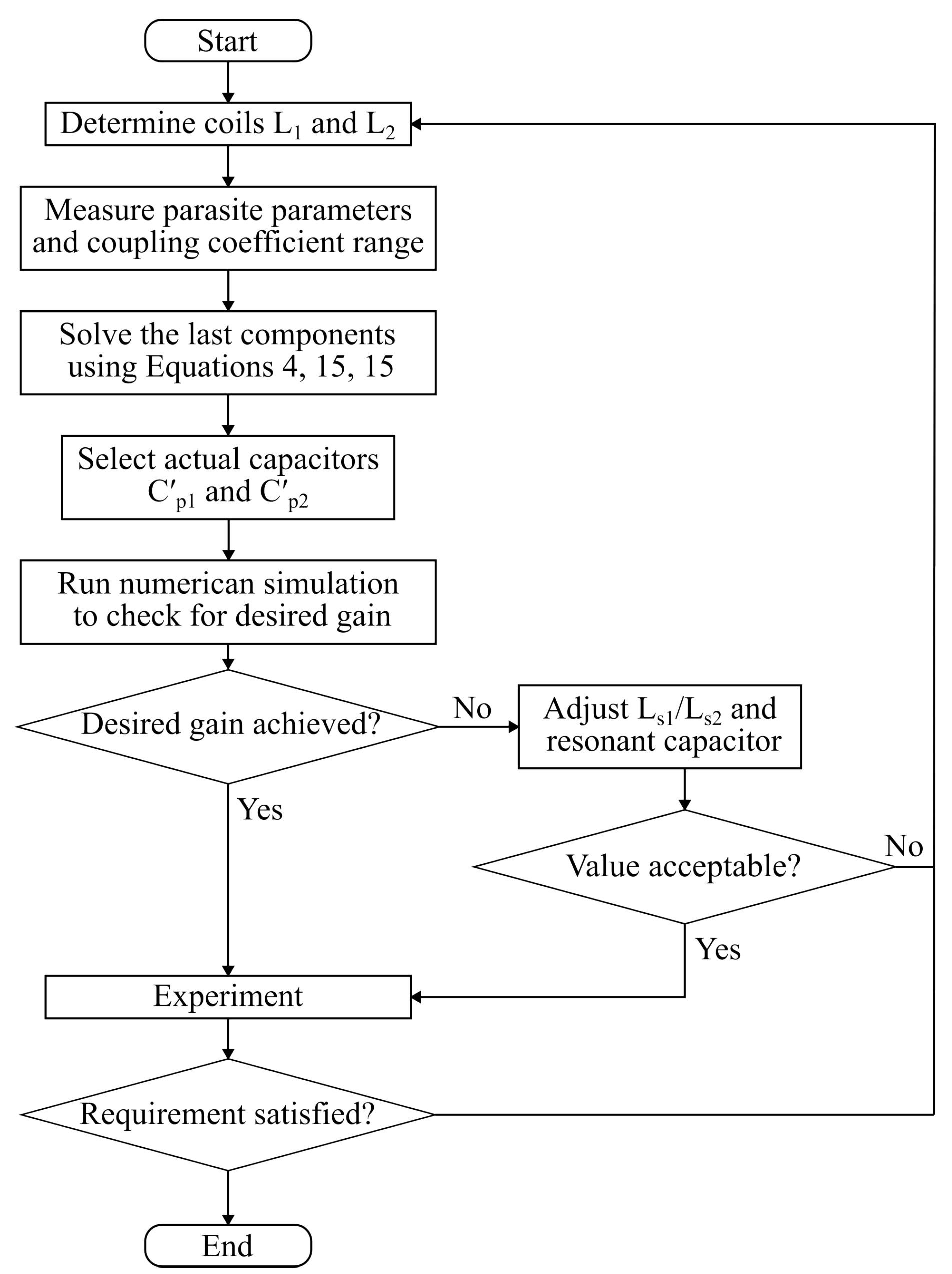
2.5. Design Procedure
The circuit in Figure 1b has seven parameters to be determined. Given that the effect of the parasite resistance is limited, the circuit can be assumed as ideal when select the LC values. Based on experiment result, iteration may be needed to account for parasite parameters, including the stray capacitance of the coils.
The coil and should be determined before designing the LCC compensation circuit. The parasite parameters of coils and their coupling coefficient range is then measured. The last 5 components can be solved by Equation (4),(5) and (15) to make the circuit resonant at , smoothen the gain slope and acquire desired gain at . The actual capacitors are selected as and . A numerical simulation based on Equation (3) to check weather the desired gain is achieved. when not, / and the corresponding resonant capacitor must be adjusted. If the adjusted value is beyond acceptance, then roll-back to the coil designing.
Figure 4.
Design flowchart
3. Results
3.1. Validation of LCL-Compensated WPT and Voltage Gain Estimation
An experiment platform of LCL-Compensated WPT circuit that works on 6.78MHz ISM band is constructed, shown in Figure 5. The coils are implemented on FR4 PCBs and of circular shape. The detailed parameters are listed in Table 1 and Table 2. To adjust the coupling coefficient, i.e. the distance between the coils, the PCBs are fixed on a 3D-printed PLA material base, with the length of the nylon columns between them adjustable.
The transmitter is driven by signal generator via SMA cable. As 0805 chip inductors are used in the compensation circuit, the driving voltage is set to 300mVpp. and are monitored by oscilloscope. To cover the internal resistance of the signal generator, is also monitored, and data is normalized as .
Two sets of data are recorded in experiment, with pure resistive load and open-circuit respectively. The recorded result and theoretical curves are plotted in Figure 6.
4. Discussion
4.1. Discussion of experiment result
The recorded data in Figure 6 shows that the characteristic of experiment circuit follows the identical trend as that of the mathematical model proposed in section 2. The effect of load changes on the estimation is limited, but still observable. Data points of load deviate from the theoretical curve farther, as the parasite parameters vary at the frequency higher than those at which they were measured.
Noises occurred in the measurement has affected the recorded data, creating inconsistent points. Such noises are expected to appear in applications as well. Averaging may be required to ensure the accuracy of the estimation. Additionally, as the independency of resonant voltage gain is slightly weaker than expected due to complex parasite parameters, should be measured during intervals of transmission with lower , based on Equation (7). The new estimation strategy is shown in Figure 7.
4.2. Application
The proposed CV-WPT strategy is planned to be implemented in an implant neural stimulating system shown in Figure 8. To achieve bipolar current stimulation, the system uses amplitude modulation (AM) to transfer power. A threshold voltage is established in the implant stimulator. When the demodulated AM signal surpasses the threshold, the stimulator outputs positive current and vice versa. This procedure is referred as Polarity Recovery. The aforementioned CV-WPT techniques provides robust and precise control with varying k. We use a linear transmission circuit built by Direct Digital Synthesis (DDS) and High-Power Output Current Feedback Amplifier (CFA) for better accuracy, with a trade-off of efficiency.
The MCU uses two LUTs to estimate the received voltage. First of them is derived from Equation (11), it estimates basing on measured . The other is derived from Equation (18) and outputs the corresponding of given . The desired is calculated by , and sent to the DDS. The intermediate is also used to detect misalignment or fault.
5. Conclusion
The LCL-Compensated WPT circuit is re-analysis for constant voltage transmission. The proposed CV-WPT system uses voltage measures on the transmitting side to estimate the coupling coefficient and voltage gain. Its feasibility is proved and the load-independent characteristic is validated through experiment. Compared to existing methods, our approach does not require frequency sweep or bulky components such as RF relays. The tuning strategy helps further shrink the size of the implant receiver.
Author Contributions
Conceptualization, Zhiyang Cao, Shicong Gui, Chujia Xu and Yubo Li; Formal analysis, Zhiyang Cao; Investigation, Chujia Xu, Rui Zhong and Zhaotan Lin; Project administration, Yubo Li; Resources, Yubo Li; Software, Rui Zhong and Zhaotan Lin; Supervision, Yubo Li; Validation, Zhiyang Cao; Writing – original draft, Zhiyang Cao; Writing – review & editing, Shicong Gui. All authors have read and agreed to the published version of the manuscript.
Funding
This research was funded by Key R&D Program of Zhejiang Province grant number 2022C03038; BLB19J014.
Data Availability Statement
The data presented in this study are available on request. Please connect the corresponding author.
Acknowledgments
We gratefully acknowledge the support and collaboration of Qizhen Taichi Medical Co, Ltd.
Conflicts of Interest
The authors declare no conflicts of interest.
References
- Haerinia, M.; Shadid, R. Wireless Power Transfer Approaches for Medical Implants: A Review. 1, 209–229. Number: 2 Publisher: Multidisciplinary Digital Publishing Institute. [CrossRef]
- Niu, W.Q.; Chu, J.X.; Gu, W.; Shen, A.D. Exact Analysis of Frequency Splitting Phenomena of Contactless Power Transfer Systems. 60, 1670–1677. [CrossRef]
- Feng, H.; Cai, T.; Duan, S.; Zhao, J.; Zhang, X.; Chen, C. An LCC-Compensated Resonant Converter Optimized for Robust Reaction to Large Coupling Variation in Dynamic Wireless Power Transfer. 63, 6591–6601. Conference Name: IEEE Transactions on Industrial Electronics. [CrossRef]
- Xiao, C.; Cheng, D.; Wei, K. An LCC-C Compensated Wireless Charging System for Implantable Cardiac Pacemakers: Theory, Experiment, and Safety Evaluation. 33, 4894–4905. Conference Name: IEEE Transactions on Power Electronics. [CrossRef]
- Li, S.; Li, W.; Deng, J.; Nguyen, T.D.; Mi, C.C. A Double-Sided LCC Compensation Network and Its Tuning Method for Wireless Power Transfer. 64, 2261–2273. Conference Name: IEEE Transactions on Vehicular Technology. [CrossRef]
- Wang, X.; Xu, J.; Mao, M.; Ma, H. An LCL-Based SS Compensated WPT Converter With Wide ZVS Range and Integrated Coil Structure. 68, 4882–4893. Conference Name: IEEE Transactions on Industrial Electronics. [CrossRef]
- Gupta, R.; Samanta, S. A Novel Parameter Tuning for LCL–LCL WPT With Combined CC/CV Charging and Improved Harmonic Performance. pp. 1–11. [CrossRef]
- Abou Houran, M.; Yang, X.; Chen, W. Magnetically Coupled Resonance WPT: Review of Compensation Topologies, Resonator Structures with Misalignment, and EMI Diagnostics. 7, 296. Number: 11 Publisher: Multidisciplinary Digital Publishing Institute. [CrossRef]
- Yang, C.L.; Chang, C.K.; Lee, S.Y.; Chang, S.J.; Chiou, L.Y. Efficient Four-Coil Wireless Power Transfer for Deep Brain Stimulation. 65, 2496–2507. Conference Name: IEEE Transactions on Microwave Theory and Techniques. [CrossRef]
- Jiang, D.; Cirmirakis, D.; Schormans, M.; Perkins, T.A.; Donaldson, N.; Demosthenous, A. An Integrated Passive Phase-Shift Keying Modulator for Biomedical Implants With Power Telemetry Over a Single Inductive Link. 11, 64–77. Conference Name: IEEE Transactions on Biomedical Circuits and Systems. [CrossRef]
- Chen, Q.; Wong, S.C.; Tse, C.K.; Ruan, X. Analysis, Design, and Control of a Transcutaneous Power Regulator for Artificial Hearts. 3, 23–31. Conference Name: IEEE Transactions on Biomedical Circuits and Systems. [CrossRef]
- Li, J.; Zhang, X.; Tong, X. Research and Design of Misalignment-Tolerant LCC–LCC Compensated IPT System With Constant-Current and Constant-Voltage Output. 38, 1301–1313. Conference Name: IEEE Transactions on Power Electronics. [CrossRef]
- Yao, L.; Zhao, J.; Li, P.; Liu, X.; Xu, Y.P.; Je, M. Implantable stimulator for biomedical applications. 2013 IEEE MTT-S International Microwave Workshop Series on RF and Wireless Technologies for Biomedical and Healthcare Applications (IMWS-BIO), pp. 1–3. [CrossRef]
- Kim, J.D.; Sun, C.; Suh, I.S. A proposal on wireless power transfer for medical implantable applications based on reviews. 2014 IEEE Wireless Power Transfer Conference, pp. 166–169. [CrossRef]
- Beh, T.C.; Kato, M.; Imura, T.; Oh, S.; Hori, Y. Automated Impedance Matching System for Robust Wireless Power Transfer via Magnetic Resonance Coupling. 60, 3689–3698. Conference Name: IEEE Transactions on Industrial Electronics. [CrossRef]
Figure 1.
LCL-compensated WPT structure(a) and its equivalent circuit model(b)
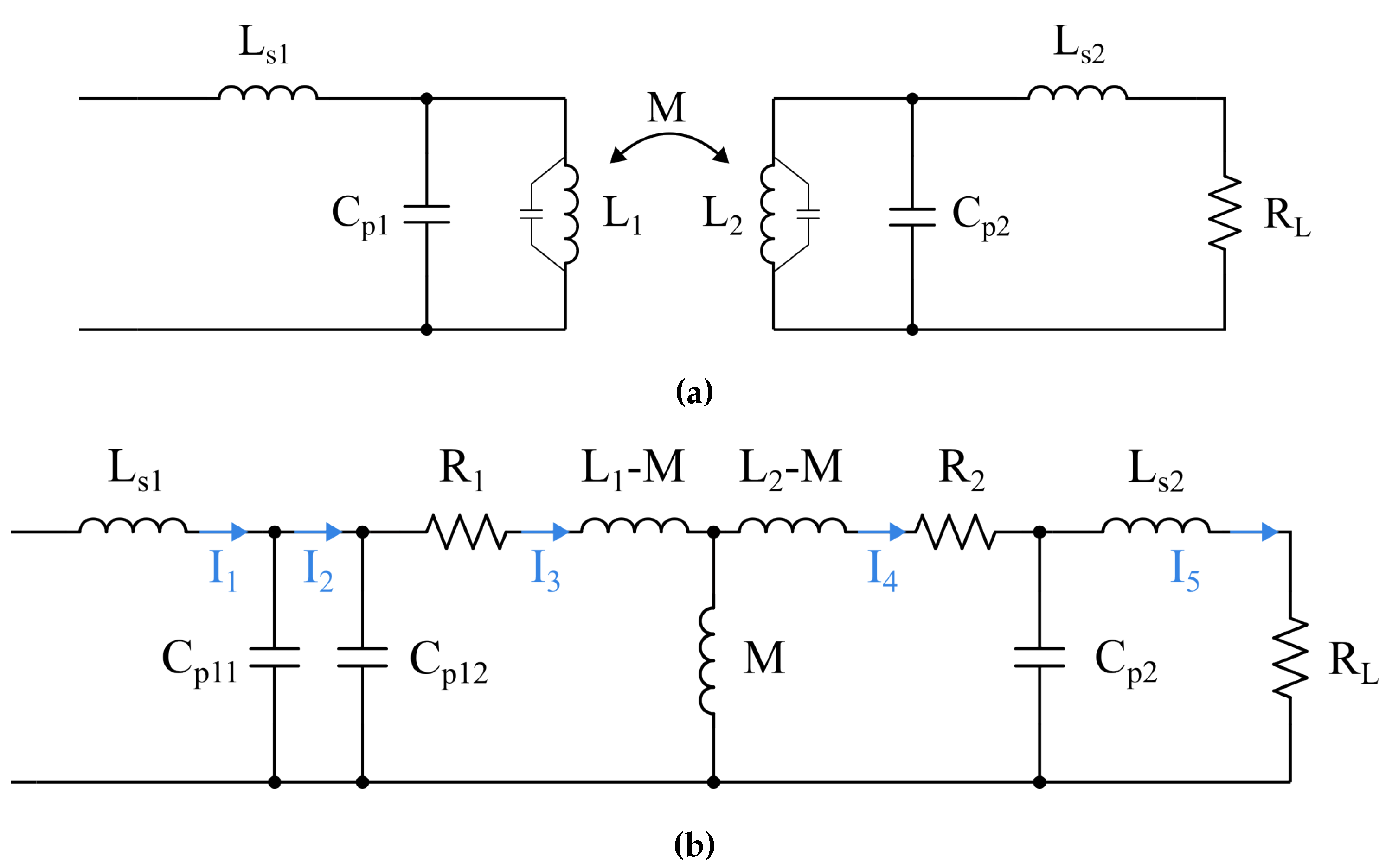
Figure 2.
-G-k relationship with , , at 13.56MHz
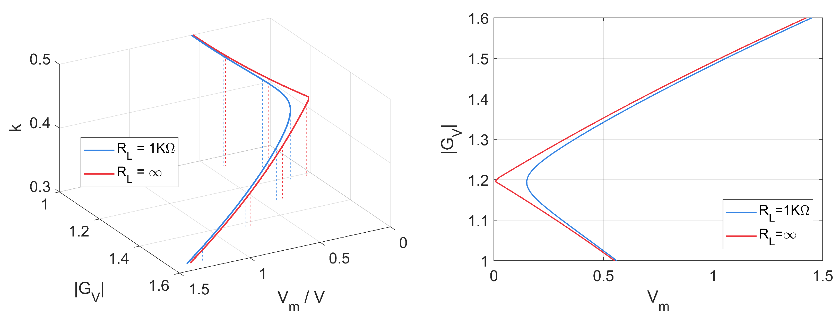
Figure 3.
Minimized gain slope by Equation (15)
Figure 3.
Minimized gain slope by Equation (15)
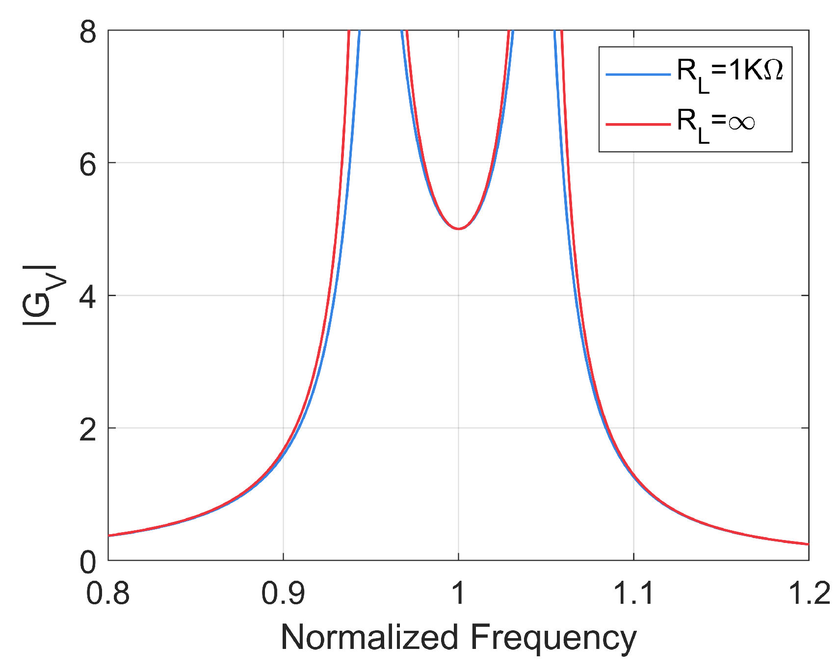
Figure 5.
Experiment PCBs(a) and 3D-printed base(b)
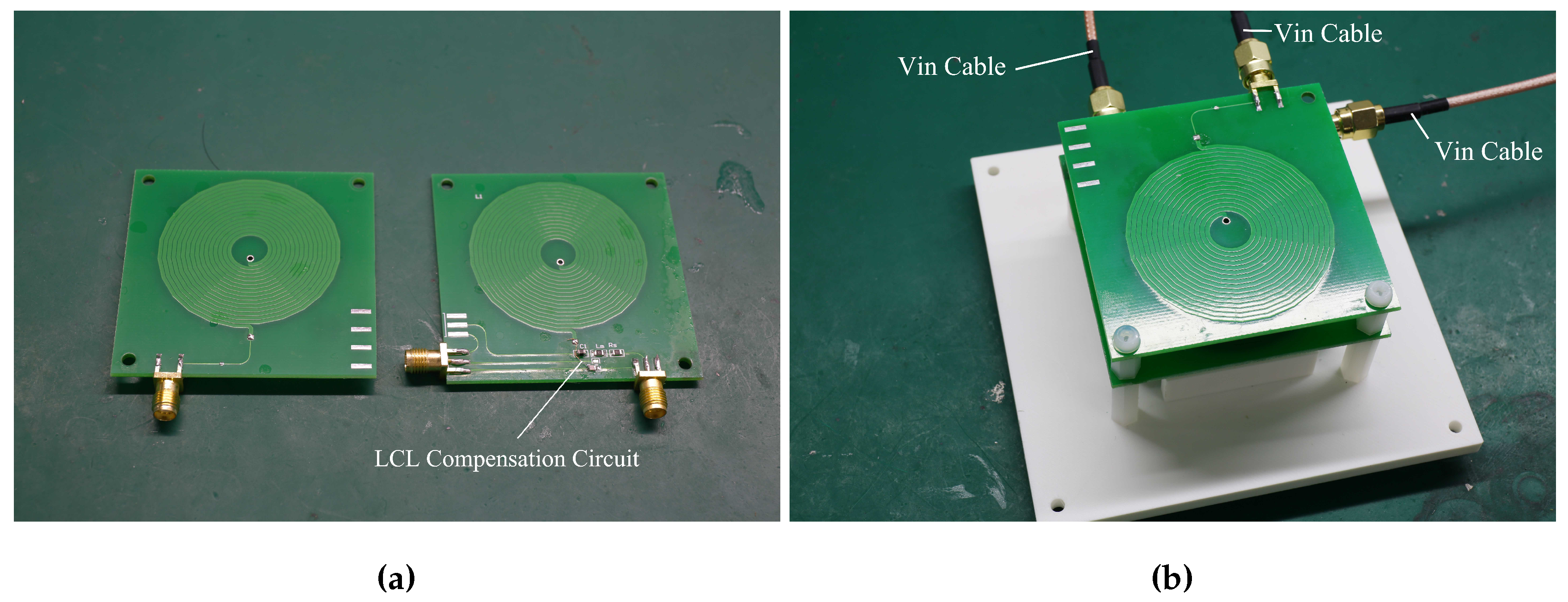
Figure 6.
Simulated and recorded - of the experiment circuit, with parameters in Table 2
Figure 6.
Simulated and recorded - of the experiment circuit, with parameters in Table 2
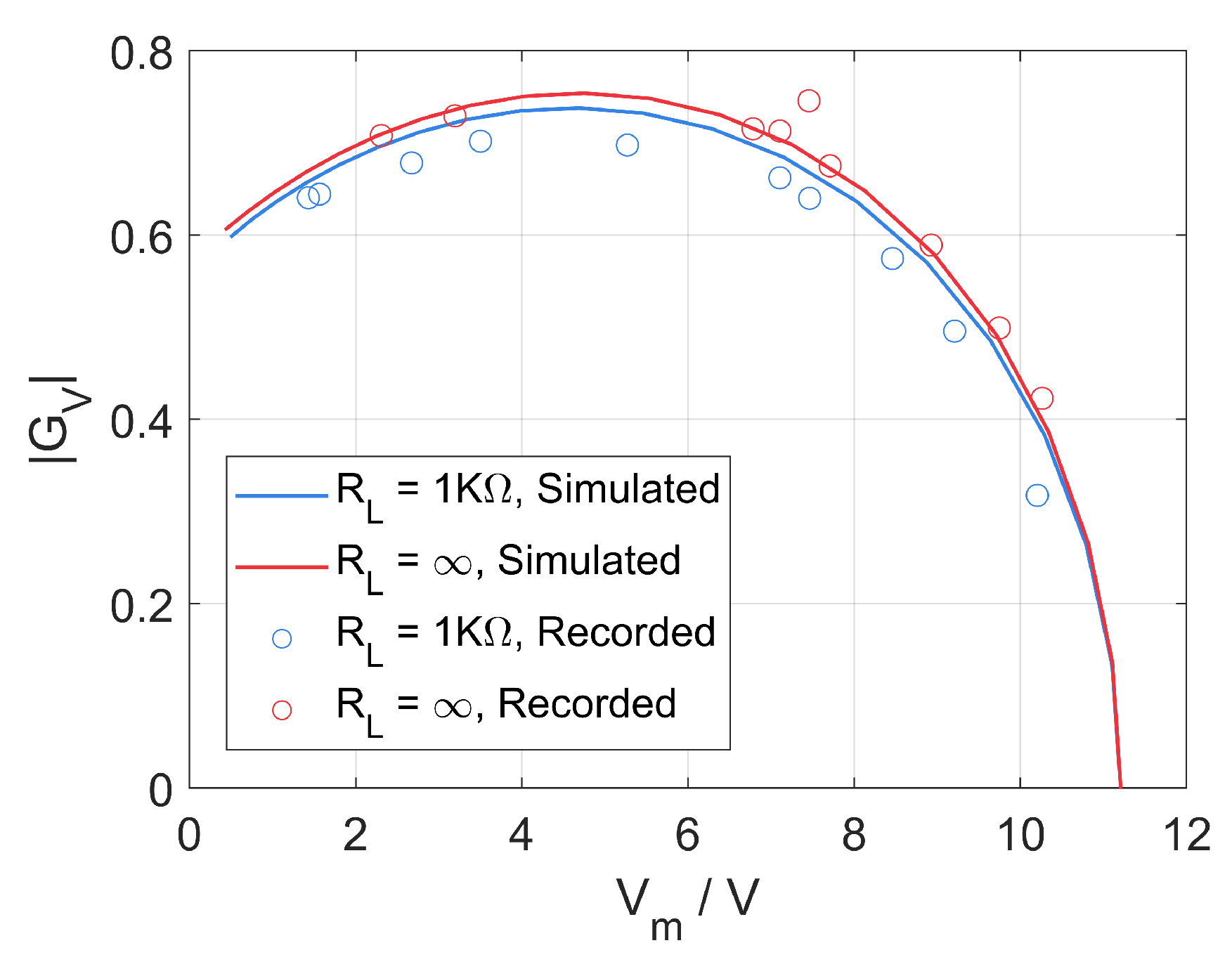
Figure 7.
CV-WPT with estimation strategy
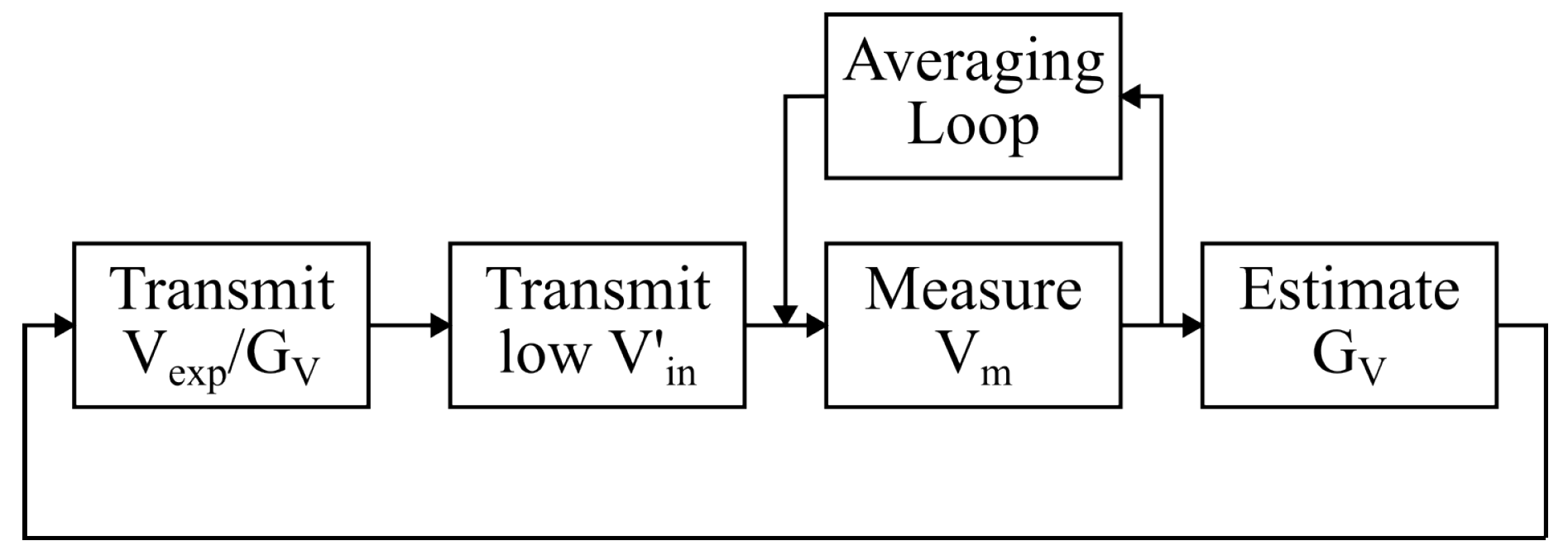
Figure 8.
Functional diagram of proposed wireless stimulation system
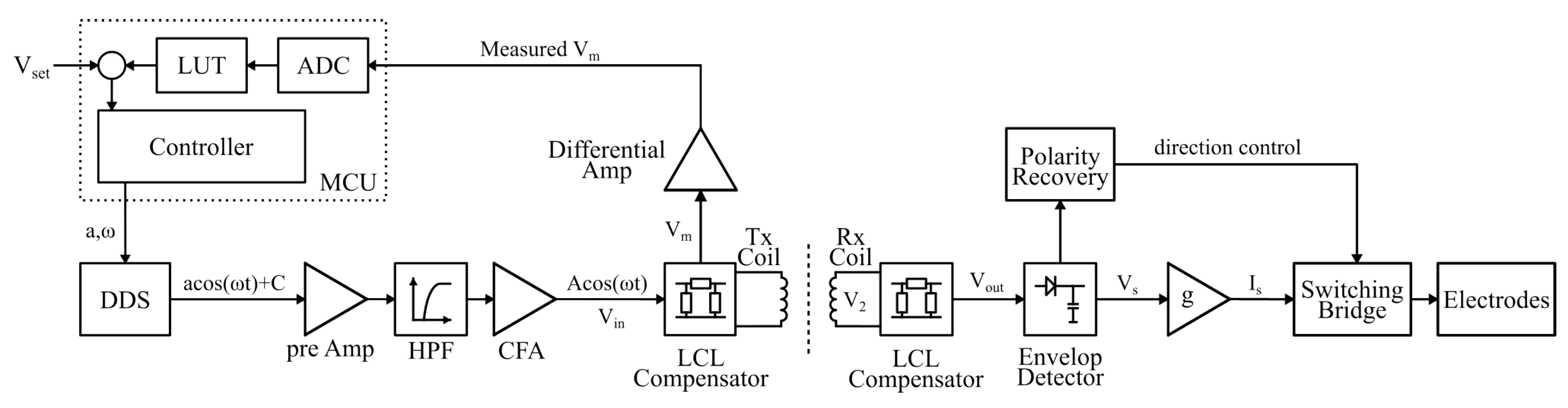

Table 1.
Parameters of the PCB coil
| Parameter | Value |
|---|---|
| Outer diameter | 44.8mm |
| Inner diameter | 8.6mm |
| Number of turns | 32 |
| Wire width | 40mil (1.016mm) |
| Wire thickness | 1.37mil (0.0348mm)1 |
| Wire spacing | 5mil (0.127mm) |
| Board thickness | 1.6mm |
1 1 Oz copper.
Table 2.
Parameters of the experiment circuit
| Component | Value |
|---|---|
| 22.2H 1 | |
| 22.3H 1 | |
| 14.7H 1 | |
| 5.64H 1 | |
| 15pF 2 | |
| 15pF 2 | |
| 59.9pF 1 | |
| 93.8pF 1 | |
| 35.0 2 | |
| 12.6 2 | |
| 3.24 1 | |
| 3.31 1 |
1 Measured by LCR meter at 100kHz. 2 Measured by VNA at 6.78MHz.
Disclaimer/Publisher’s Note: The statements, opinions and data contained in all publications are solely those of the individual author(s) and contributor(s) and not of MDPI and/or the editor(s). MDPI and/or the editor(s) disclaim responsibility for any injury to people or property resulting from any ideas, methods, instructions or products referred to in the content. |
© 2024 by the authors. Licensee MDPI, Basel, Switzerland. This article is an open access article distributed under the terms and conditions of the Creative Commons Attribution (CC BY) license (http://creativecommons.org/licenses/by/4.0/).
Copyright: This open access article is published under a Creative Commons CC BY 4.0 license, which permit the free download, distribution, and reuse, provided that the author and preprint are cited in any reuse.


