Submitted:
03 May 2024
Posted:
06 May 2024
You are already at the latest version
Abstract
In the present work, diamond films have been grown on GaN-on-Sapphire substrates by chemical vapor deposition (CVD) with the addition of nitrogen to the standard H2/CH4 precursor recipe. Diamond on GaN materials processing is not straight-forward, as GaN is susceptible to a quasi-pure hydrogen CVD plasma etching. 1%, 3% and 5% N2 gas was gradually added to the H2 gas with fixed 6% CH4 in the recipe to promote the growth of diamond nanocrystals. Different types of microstructures were produced, with addition of nitrogen to the precursor gas recipe. Nitrogen gas changes the diamond film microstructure from faceted to spherical grains, with signs of GaN etching. The sp3 bonded diamond film produced by nitrogen addition was found to be co-deposited along with a considerable amount of other non-diamond carbon phases (D - disordered graphite, G - crystalline graphite, TPA - trans-polyacetylene) and qualitatively all the diamond films were 50% pure (Raman peak ratio Isp3 / ID). The FWHM of the sp3 carbon Raman peak was calculated to be 6.5 cm-1, when there was no nitrogen gas in the precursor recipe, which deteriorates to a large extent after successive addition of N2. Fourier transform infrared spectroscopy (FTIR) showed a strong presence of the nitrogen related defects (peak positions at 1190 and 1299 cm-1) inside the nanocrystalline diamond (NCD) films grown with N2 addition. GaN layer etching from the base substrate by the CVD plasma was clearly evidenced by energy dispersive X-ray spectra (EDS) of the deposited films. Al elemental EDS peaks from the base sapphire substrate were observed for the films grown with nitrogen addition, but no Ga EDS peaks were detected. X-ray diffraction (XRD) micrographs further supported the enhanced GaN etching phenomenon. Nitrogen addition was thus found to be detrimental for growing CVD diamond films over GaN surfaces. The electrical resistivity of the uncoated GaN was initially measured to be 22.2 Ω-cm. However, the resistivity rose to 1.59×10⁶ Ω-cm after the nitrogen assisted film deposition; due to the GaN etching - thereby exposing the underlying insulating sapphire substrate.
Keywords:
CVD
; etching
; diamond
; GaN
; microstructure
; properties
1. Introduction:
GaN is used in high power electronics applications [1,2]. Its success in realizing wide industrial application depends on the effective heat dissipation of the GaN electronics [3]. One of the approaches to remove the heat is to integrate GaN having lower thermal conductivity (110 W/m-K) with the best heat conducting material, i.e., diamond (single crystals can have as high as 2000 W/m-K thermal conductivity at room temperature) [4,5]. However, combining GaN directly with diamond [6] is not possible due to incapability of the material to form a carbide. The ideal scenario is the deposition of chemical vapor deposition (CVD) diamond onto a GaN substrate [7] with H-terminated nanodiamond seeding technique, for a favorable surface zeta potential value. However, there are film adhesion problems associated with the direct growth of diamond on GaN, in comparison to the other nitride materials, like AlN [8]. Moreover, the harsh CVD processing conditions inside the diamond growth reactors reportedly etches the GaN material due to chemical reactions with the hydrogen plasma [9].
GaN and diamond are both wide band gap semiconductors with band gap values of 3.44 eV and 5.45 eV, respectively [10,11,12,13,14,15,16,17,18,19]. On the other hand, silicon has an intrinsic band gap of 1.12 eV with electron and hole mobilities of 1400 and 450 cm2/Vs, respectively. Silicon has a thermal expansion coefficient of 2.6 ppm/K with a thermal conductivity of 130 W/m-K (at room temperature) - closely matching with GaN but widely different from diamond. The critical break down field is the best for diamond 6×10⁶ V/cm, while GaN is almost half of that value at 3×10⁶ V/cm. Si is getting replaced in high power, high frequency and high temperature electronics by such wide bandgap semiconductors, due to its one order lower break down field of 3×10⁵ V/cm. The principal reason behind putting diamond in conjugation with GaN is to take away the generated heat from the power electronics. It will be an added advantage if the deposited diamond can also be made conducting where it can even be used as electrode or the diamond material itself can be used as a wide band gap semiconductor, replacing and/or enhancing properties of GaN power electronics. Nitrogen has been tried to induce n-type doping conductivity [20] in diamond but with limited success, due to the creation of a deep donor level [21]. However, nitrogen induces diamond re-nucleation, which can show other interesting electrical properties [22]. Nitrogen promotes higher growth rates of diamond films and thereby creates smaller grain sizes [23]. The graphitic and other non-diamond carbon phases that are present in the grain boundaries of the different diamond morphologies [24], grown with nitrogen gas addition in the CVD precursor recipe, are expected to induce electrical conductivity [25]. But there is as such no study in attempting direct deposition of conducting diamond films on GaN substrates, with nitrogen gas in the growth recipe. One of the reasons, is that growing diamond on GaN leads to surface chemical reactions [9]. The other reason is that the diamond on GaN technology [26] is not fully developed to exploit its versatile properties, in different combinations. Whereas, semiconducting diamond can be synthesized by using boron, nitrogen and/or phosphorous dopants [27] during the CVD deposition. The nitrogen atom has been reported to improve the grain boundary conductivity by promoting an (ultra)nanocrystalline diamond (NCD) morphology [28]. However, there is no literature on the properties of diamond on GaN films, while adding N2 to the CVD recipe for growth. In this work diamond is grown on GaN substrates by using different gas recipes, while keeping in mind its potential application in electronics.
2. Materials and Methods:
Table 1 describes the processing parameters for growing CVD diamond films with different precursor gas recipes. The as-received GaN/Sapphire substrates (from commercial suppliers) were first CF4 plasma treated for modifying the surface zeta potential [29], which is conducive for subsequent water suspension-based detonation nano-diamond (DND) seeding, as described earlier in literature [30]. Thereafter, the substrates were loaded into the 2.45 GHz resonant cavity CVD reactor chamber (ASTeX 6500) [31]. The starting base pressure before each CVD run was 3.7×10⁻³ Torr. The working pressure was 55 Torr and the total gas flow rate was 300 sccm, with 3000 W input microwave power. A flat type of molybdenum substrate holder was used which produced a substrate temperature of 600oC under these process parameters, as measured in-situ by a double wavelength optical pyrometer (Williamson, model no. PRO 92-400C). The methane percentages were fixed at 6% and the nitrogen gas was introduced gradually into the CH4/H2 precursor recipe by decreasing the H2 percentages as described in Table 1. Each CVD deposition was carried out for 2-hour long duration (Table 1, #D0-5).
Table 1 shows four sets of diamond films (D) which have been identified as per the nitrogen percentages (0-5 in the suffix) used inside the resonant cavity CVD reactor. The grown films were characterized by scanning electron microscope (SEM-FEI Quanta 200 FEG) for microstructure evaluation along with energy dispersive X-ray spectroscopy (EDS) for identifying the elements that are present on the CVD grown film surfaces. Raman spectroscopy (HORIBA Jobin Yvon T64000 spectrometer using laser light of 488 nm wavelength) was used to determine the different non-diamond carbon phases that are deposited along with the sp3 bonded diamond. Fourier transform infra-red spectroscopy (FTIR, Bruker- INVENIO R) revealed the different chemical bonds that exist in the CVD grown diamond film structure. X-ray diffraction (XRD) was performed with a Bruker D8 theta-theta diffractometer, equipped with a Göbel mirror (line focus, mostly Cu ka radiation). The X-rays are detected with a 1D lynxeye detector. X-ray scan was from 10º to 80º 2θ range, with 0.04º stepsize and 10 sec/step counting time. The electrical resistivity of the composite film structure (diamond on GaN/Sapphire) was measured by the Hall measurement technique [32], for 6×6 mm2 square shaped samples, based on conformal mapping method, developed by van der Pauw [33,34]. The contacts (pin material: tungsten carbide, pin tip radius: 200 μm) were at the circumference of the sample and were sufficiently small.
3. Results and Discussion:
3.1. Diamond Film Morphology - SEM
Different types of nanocrystalline diamond microstructures were produced over GaN/sapphire substrates (Figure 1), while increasing the N2 percentages in the precursor recipe from 0% to 5%. Nitrogen gas changes the diamond film microstructure from faceted (Figure 1d & 1e, #D0) to spherical grains (Figures 1a - #D1, 1b - #D3 & 1c - #D5) with possibility of GaN substrate etching, which will be explained later. When there was no nitrogen in the precursor gas recipe, i.e., 6% CH4 in 94% H2, well faceted diamond grains were produced (mostly octahedrals, Figure 1e) of approximately average 0.5 μm sizes. Whereas, with the introduction of nitrogen gas in the precursor recipe, the microstructure changes to spherical grains as found in Figure 1a, 1b and 1c. 1% N2 in the precursor recipe produced closely packed spherical diamond grains with average sizes of approximately 2 μm (Figure 1a). 3% N2 increased the growth rate of diamond resulting in reduced spherical grain sizes of approximately 0.7-1 μm. Figure 1b also revealed intergranular pores in the microstructure of the diamond films. Such internal pores become very big, exposing the underlying substrate surface with the addition of 5% N2 in the precursor recipe, as found in figure 1c. Its morphology looks very much similar to the non-coalesced diamond films, showing typical features of early nucleation and growth stages. The average diameter of the individual diamond spheres is approximately 0.8-1.2 μm (figure 1f) and they do not differ much from Figure 1b with 3% N2. Such individual spheres at higher magnification of 100kX (Figure 1f) are found to be cauliflower like or ballas type diamonds, made from smaller nanocrystals.
Figures 2a-2c are the NCD microstructures at 25kX magnification on Si substrates kept alongside the GaN/sapphire substrate during the CVD deposition. Successive addition of 1%-5% N2 does not change the microstructural features of the NCD films on Si. On magnifying the NCD microstructures further under SEM at 100kX, it is found to consist of densely populated nanocrystalline diamond grains, without any intermediate pores or appearance of the underlying substrate. However, when the microstructure of NCD on GaN/Sapphire (Figure 1) is compared with those on Si (Figures 2a-d), it appears to differ in two aspects. First is that the shapes of the diamond grains are different. NCD on GaN at 3% N2 addition (samples #D3) is found to be spherical or ballas type whereas, NCD on Si at 3% N2 addition is found to be irregular in shape. The average size of the spherical NCDs on GaN was approximately 0.7-1 μm (Figures 1b and 2e), while, the average size of the irregular shaped NCD grains on Si was also found to be approximately of the same size, as shown in Figure 2b. At the higher magnification, such apparently bigger micron sized diamond grains on Si (Figure 2c) appear to consist of 100-150 nm tiny diamond nanocrystals as shown in Figure 2d. If the equally magnified images of the spherical diamond on GaN films (Figures 1f and 2e) are compared with the irregular shaped NCDs on Si (Figure 2d), then the film on GaN/sapphire substrate also appears to have similar tiny diamond nanocrystals on its spherical surface. Therefore, it is found that although the NCD shapes are different their sizes are almost equivalent on both the Si and GaN/Sapphire substrates. The second striking difference between the NCD on Si and the NCD on GaN, is the gradual appearance of the underlying substrate with successive increase in nitrogen percentages for the NCD grown over GaN/Sapphire substrates, with a non-coalesced film morphology. On Si, unlike GaN/Sapphire, the diamond film coalesced and the underlying silicon substrate was never exposed with the successive nitrogen gas addition in the CVD precursor recipe.
3.2. Film Surface Characterisation - EDS
In order to evaluate the nature of the exposed surface and the corresponding CVD grown diamond films on GaN/sapphire substrates, EDS elemental analysis was done by area scan. Figure 3a and 3d are the EDAX peaks from the NCD films #D1 and #D0. Both of the EDS spectra show a signal only corresponding to carbon (C). The only contrast between them is that the respective individual C peak counts/intensity are different. Figure 3b is the EDS spectrum of the NCD film on GaN/sapphire substrate for 3% N2 in the CVD precursor gas recipe. SEM images 1b and 2e earlier showed that there were pores present in between the spherical diamond grains. EDS from such porous film not only produced the C elemental peak but also a small Al element peak at 1.49 eV was detected, corresponding to the sapphire substrate. Surprisingly, the EDS peak from a heavy element like Ga was absent. Moreover, the EDS did not detect any N elemental peak from the substrate, which should have been present from the NCD grown over the GaN surface, along with the appearance of the intergranular pores. May et al. [9] in their earlier effort to deposit diamond films on GaN surfaces using hot filament CVD, proposed the following three chemical reactions under the typical diamond CVD growth conditions:
2N (surface) + 3H2 (g) ↔ 2NH3 (g)
2Ga (surface) + H2 (g) ↔ 2GaH (g)
2GaN (s) ↔ Ga(l) + N2(g)
The H2 gas in the CVD diamond growth precursor recipe reacts with Ga and N on the substrate surface to produce gaseous by-products, which escape the film surface creating pores in the microstructures. Moreover, if the CVD growth temperature is high enough it can even dissociate solid GaN material into Ga and N2 respectively. With the non-presence of elemental Ga from the EDS spectra of the NCD on GaN/Sapphire substrate (Figure 3), it can be concluded that there is no Ga left. All the Ga must have reacted with the hydrogen plasma to escape into the gas phase. Surprisingly with the increased addition of N2 at 5%, there is a stronger appearance of Al and O elemental EDS peaks (Figure 3c) from the underlying base sapphire layer - but no elemental signature from the top substrate layer of GaN, which should have been present before appearance of any bottom layer sapphire peaks. This definitively shows that the nitrogen gas addition adversely affects the CVD plasma chemical reactions with the GaN surfaces by completely etching them out. Presence of nitrogen might have favoured the forward reaction 3, which resulted in more GaN to dissociate and thereby helping more hydrogen plasma etching of the Ga & N elements from the top substrate surface (forward reactions 1 and 2). EDS spectra 3c corresponds to the NCD microstructure image 2f (#D5). Therefore, the exposed surface that gradually started to appear is the underlying sapphire substrate with the disappearance of its top GaN layer.
3.3. Diamond Film Quality – Raman Spectroscopy
Figure 4 shows the Raman spectra of the diamond films [35] grown on GaN/Sapphire substrates (samples #D0-5). The Raman spectrum of the film (#D1) grown with 1% N2 (Figure 1a) in the precursor recipe produced sharp 1140 cm-1 signal (ν1) corresponding to nanocrystalline diamond crystallites. The sharpness and intensity of the ν1 peak position successively get reduced in Figures 1b and 1c, as the N2 percentages are increased to 3% (#D3) and 5% (#D5), respectively. This gradual variation in the nature of the ν1 peak indicates the re-nucleation characteristics of the diamond nanocrystals. Moreover, there is a slight shift in ν1 position to 1143 cm-1 for the NCD grown over GaN/Sapphire with 5% N2 – which is attributed to the complete etching out of the GaN layer with the appearance of the non-coalesced film microstructures (Figures 1c & 2f). Whereas, the typical ballas type NCD grains (Figures 1a and 1b) produced sharp nanocrystalline diamond peaks at the typical position of 1140 cm-1. Even the well facetted diamond grains (Figure 1d & 1e) produced the typical ν1 peak at the exact position of 1140 cm-1. The sample #D0 was grown with a relatively high proportion of 6% CH4 in the gas recipe, therefore such nano-diamond peaks are expected. There is also the appearance of the trans-polyacetylene (TPA) peaks at 1480 cm-1 for the diamond films #D1 and #D3. However, by changing the N2 percentages from 1% to 3%, the TPA peak absolute intensities are altered in comparison to the bumps around 1540 cm-1 (Figure 4a) or 1535 cm-1 (Figure 4b), which are due to the crystalline graphitic (G) inclusion in the film. Such G peak is further intensified (Figure 4c) when 5% N2 is used in the precursor recipe, with the appearance of the non-coalesced NCD microstructure (Figure 2f). The TPA peak relative intensity is also much suppressed in comparison to the G peak for the sample #D5. Whereas, it is the opposite, i.e., the relative intensities of the TPA peaks are higher than the G peak intensities for the samples #D0, #D1 and #D3. Each of the films clearly shows the sp3 diamond peak at 1332 cm-1, exception being the NCD film grown with 5% N2, where the sp3 peak is shifted to 1334 cm-1. The sp3 peak is always detected together with the disordered graphite (D) peak around 1350 cm-1. The relative Raman spectra intensities of sp3 peak (Isp3) to the disordered graphite sp2 peak (ID) was found to be always 50% (Figures 4a-c) for the NCD grown with 1%, 3% and 5% N2 addition. The NCD grown without (0%) N2 addition, showing a clear facetted crystalline nature (Figure 1d & 1e), leads to a relative diamond peak intensity Isp3 / ID of 59% (Figure 4d) and sp3 peak FWHM of 6.5 cm-1.
3.4. Chemistry of the Deposited Film - FTIR
Figure 5 shows the FTIR spectra of the diamond films grown with variable percentages of nitrogen in the precursor recipe. There are multiple peaks from the films which are several microns thick grown over 2 hrs of deposition time. The most prominent peak at 1190 cm-1 is due to the N-defect or the so-called aggregated nitrogen atoms in the tetrahedron form known as the B-defect centre, and the other prominent peak at 1299 cm-1 is due to the aggregated nitrogen atoms in platelet form known as the A-defect centre, inside the diamond cubic crystal lattice. The peak(s) at 1428 cm-1 or 1464 cm-1 are assigned to the bending or deformation of the C-H bonds [36]. The peaks at 612 cm-1 and 1103 cm-1 are due to the contamination of the CVD grown diamond film from the underlying substrate material [37]. 612 cm-1 is believed to be from the Ga-N bond stretching which appeared in Figures 5a and 5b for the samples #D1 and #D3. Surprisingly, such Ga-N bond stretching peak disappears in the FTIR Figure 5c for the sample #D5, which again confirms the earlier findings from the Figures 2f & 3c, that the GaN etching by CVD plasma was complete to only reveal the underlying sapphire substrate base at 5% N2 concentration. Figure 5d shows the strongest Ga-N FTIR signal for the NCD grown without N2 addition. However, it is to be noted that the FTIR instrument used here had a Si beam splitter which might have produced artifact that overlapped with the GaN peak as well.
3.5. Nitrogen Addition Enhances GaN Etching – XRD & Electrical Property
Figure 6a shows that the GaN-on-sapphire substrate produces a very strong peak of GaN face-centred cubic crystal structure from (111) planes, with interplanar spacing 4.5 Å at 34.4º 2θ angle of diffraction (JCPDS file no. 52-0791). On the other hand, the XRD signal from the base sapphire substrate at 41.6º 2θ angle, due to the reflection from (200) plane (JCPDS file no. 42-1468), was not very strong. Since the sapphire was underneath the GaN, it could not produce strong XRD peak in Figure 6a. However, after the CVD diamond deposition on the same GaN-sapphire substrates (sample #D5), the corresponding XRD diffraction micrograph in Figure 6b, does not show any GaN X-ray peak; but it produces only Al2O3 peak from the sapphire base. There is no X-ray signal from the top diamond film #D5, as glancing angle XRD technique was not used. It is again becoming evident that 5% N2 in the precursor recipe completely etched out the top GaN layer, thereby exposing the underlying sapphire substrate.
The electrical resistivity of the uncoated GaN-on-sapphire substrate (as-received from the commercial suppliers), measured by four-point probe method, was found to be 22.2 Ω-cm. Sapphire is the insulating base layer on top of which about 2 μm thick n-type GaN was deposited by the manufacturer, with a metal organic CVD (MOCVD) processing. The NCD film grown on GaN/sapphire substrate with 6% methane (#D0) inside resonant cavity 2.45 GHz microwave plasma enhanced CVD reactor showed a resistivity of 62.7 Ω-cm, which is more than the bare GaN/sapphire substrate. The resistivity measurement of the CVD grown diamond films (2.5 μm thick) was done on a “non-inert” GaN/Sapphire substrate, i.e., a substrate that has contribution to the Hall measurement. The measured resistivity is not only unique to the upper NCD film, but also the substrate properties (GaN/sapphire) are reflected in the resistivity measurements. The diamond samples can be arranged in the following order of increasing resistivity: GaN/Sapphire substrate<D0<D5. The nitrogen addition in the precursor gas recipe did not help to induce enhanced conductivity in the composite film structure of diamond-on-GaN. This was due to the adverse effect of the GaN substrate etching under the nitrogen environment of the CVD plasma. It was found earlier that the GaN was completely etched out when 5% N2 was used in the recipe and the underlying sapphire substrate became exposed which is an insulator. The resultant NCD film (#D5) had a very high resistivity in the order of 1.59×10⁶ Ω-cm.
Table 2 summarizes the effect of the nitrogen addition into the CVD precursor recipe on the enhanced GaN etching phenomenon. There are increased Al EDS peak signal counts from the base sapphire substrate with the increasing percentages of N2 in the CVD recipe. The Ga-N FTIR chemical bonds, that started to appear from the growing diamond films, with increasing nitrogen percentages from 0-3%, do not follow any definite trend. However, at 5% N2 concentration, the GaN chemical reaction with the CVD plasma was complete, so that no Ga-N bond could be detected by FTIR. Such substrate contaminated diamond films were found to contain non-diamond carbons phases (graphite D, G and TPA) and their quality as assessed by Raman spectroscopy are almost equivalent, irrespective of the added N2 concentrations in the CVD process recipe. The respective diamond grain sizes of the deposited films do not follow any definitive trend, with the increasing N2 concentration in the CVD recipe.
4. Conclusions
The GaN surface of the substrate reacted with the CVD plasma diamond growth environment. A standard process gas recipe, using methane and hydrogen inside a typical resonant cavity 2.45 GHz CVD reactor, without any nitrogen addition, produced well facetted crystalline films with 0.5 μm average sized diamond grains - covering the entire GaN/Sapphire substrate surface, without any apparent porosity. With the addition of 1% nitrogen gas in the CVD precursor recipe, the morphology changed to ballas type diamond grains of 2 μm in average size, while also some pores became visible. The corresponding EDS spectra with 0% and 1% N2 addition could only detect C elements from the diamond films. As the nitrogen percentages were gradually increased to 3% and 5%, there was a gradual appearance of the Al elemental peak from the underlying sapphire substrate, pointing to etching of the GaN substrate. The resistivity of such non-coalesced films was found to be very high (106 Ω-cm), which is due to the exposure of the underlying insulating sapphire substrate. The X-ray diffraction substrate peak for GaN completely disappeared after CVD growth of diamond with 5% N2 in the precursor recipe. Therefore, nitrogen in the CVD gas recipe is detrimental for growing diamond films directly onto GaN surfaces. It can have potential application for selective etching in making lithographic pattern for GaN electronics.
Author Contributions
AKM: conceptualization, methodology, formal analysis, investigation, resources, data curation, writing—original draft preparation, writing—review and editing, visualization; GK: methodology, formal analysis, investigation, resources, writing—review and editing; WCS: conceptualization, methodology, formal analysis, investigation, resources, data curation, writing—review and editing, visualization; PP: conceptualization, methodology, formal analysis, investigation, resources, data curation, writing—review and editing, visualization; KH: conceptualization, validation, writing—review and editing, visualization, supervision, project administration, funding acquisition.
Funding
This work was financially supported by the Methusalem NANO network and the Research Foundation – Flanders (FWO) via project G0D4920N. AKM acknowledges FWO for his Postdoctoral Fellowship with grant no. 12X2919N.
Acknowledgments
We thank our colleague Prof. Jan D’Haen for providing the SEM, EDS and XRD data. All data generated or analyzed during this study are included in this published article. The datasets generated during and/or analyzed during the current study are available from the corresponding author on reasonable request.
Conflicts of Interest
The authors declare that they have no known competing financial interests or personal relationships that could have appeared to influence the work reported in this paper.
References
- Amano, H.; Baines, Y.; Beam, E.; Borga, M.; Bouchet, T.; Chalker, P.R.; Charles, M.; Chen, K.J.; Chowdhury, N.; Chu, R.; et al. The 2018 GaN power electronics roadmap. J. Phys. D: Appl. Phys. 2018, 51, 163001. [Google Scholar] [CrossRef]
- Hu, J.; Zhang, Y.; Sun, M.; Piedra, D.; Chowdhury, N.; Palacios, T. Materials and processing issues in vertical GaN power electronics. Mater. Sci. Semicond. Process. 2018, 78, 75–84. [Google Scholar] [CrossRef]
- Lee, W.S.; Lee, K.W.; Lee, S.H.; Cho, K.; Cho, S. A GaN/Diamond HEMTs with 23 W/mm for Next Generation High Power RF Application, 2019 IEEE MTT-S International Microwave Symposium (IMS), Boston, MA, USA, (2019) 1395-1398. [CrossRef]
- Cuenca, J.A.; Smith, M.D.; Field, D.E.; Massabuau, F.C.-P.; Mandal, S.; Pomeroy, J.; Wallis, D.J.; Oliver, R.A.; Thayne, I.; Kuball, M.; et al. Thermal stress modelling of diamond on GaN/III-Nitride membranes. Carbon 2021, 174, 647–661. [Google Scholar] [CrossRef]
- Mahrokh, M.; Yu, H.; Guo, Y. Thermal Modeling of GaN HEMT Devices With Diamond Heat-Spreader. IEEE J. Electron Devices Soc. 2020, 8, 986–991. [Google Scholar] [CrossRef]
- Izsák, T.; Vanko, G.; Držík, M.; Kasemann, S.; Zehetner, J.; Vojs, M.; Zaťko, B. ; Potocký,.; Kromka, A. Direct Deposition of CVD Diamond Layers on Top of GaN Membranes, Proceedings 2020, 56, 35. [CrossRef]
- Mandal, S.; Thomas, E.L.H.; Middleton, C.; Gines, L.; Griffiths, J.T.; Kappers, M.J.; Oliver, R.A.; Wallis, D.J.; Goff, L.E.; Lynch, S.A.; et al. Surface Zeta Potential and Diamond Seeding on Gallium Nitride Films. ACS Omega 2017, 2, 7275–7280. [Google Scholar] [CrossRef]
- Smith, E.J.W.; Piracha, A.H.; Field, D.; Pomeroy, J.W.; Mackenzie, G.R.; Abdallah, Z.; Massabuau, F.C.-. .-P.; Hinz, A.M.; Wallis, D.J.; Oliver, R.A.; et al. Mixed-size diamond seeding for low-thermal-barrier growth of CVD diamond onto GaN and AlN. Carbon 2020, 167, 620–626. [Google Scholar] [CrossRef]
- May, P.; Tsai, H.; Wang, W.; Smith, J. Deposition of CVD diamond onto GaN. Diam. Relat. Mater. 2006, 15, 526–530. [Google Scholar] [CrossRef]
- Daniel Francis, Martin Kuball, 14 - GaN-on-diamond materials and device technology: A review, Editor(s): Marko J. Tadjer, Travis J. Anderson, In Woodhead Publishing Series in Electronic and Optical Materials, Thermal Management of Gallium Nitride Electronics, Woodhead Publishing, 2022, Pages 295-331, ISBN 9780128210840. [CrossRef]
- Zhan, T.; Xu, M.; Cao, Z.; Zheng, C.; Kurita, H.; Narita, F.; Wu, Y.-J.; Xu, Y.; Wang, H.; Song, M.; et al. Effects of Thermal Boundary Resistance on Thermal Management of Gallium-Nitride-Based Semiconductor Devices: A Review. Micromachines 2023, 14, 2076. [Google Scholar] [CrossRef]
- Mendes, J.C.; Liehr, M.; Li, C. Diamond/GaN HEMTs: Where from and Where to? Materials 2022, 15, 415. [Google Scholar] [CrossRef]
- Wort, C.J.; Balmer, R.S. Diamond as an electronic material. Mater. Today 2008, 11, 22–28. [Google Scholar] [CrossRef]
- Kohn, E.; Denisenko, A. Concepts for diamond electronics. Thin Solid Films 2007, 515, 4333–4339. [Google Scholar] [CrossRef]
- Markham, M.; Dodson, J.; Scarsbrook, G.; Twitchen, D.; Balasubramanian, G.; Jelezko, F.; Wrachtrup, J. CVD diamond for spintronics. Diam. Relat. Mater. 2011, 20, 134–139. [Google Scholar] [CrossRef]
- Ueda, K.; Soumiya, T.; Asano, H. Ferromagnetic Schottky junctions using diamond semiconductors. Diam. Relat. Mater. 2012, 25, 159–162. [Google Scholar] [CrossRef]
- Ueda, K.; Kawamoto, K.; Asano, H. High-temperature and high-voltage characteristics of Cu/diamond Schottky diodes. Diam. Relat. Mater. 2015, 57, 28–31. [Google Scholar] [CrossRef]
- Isberg, J.; Ferro, G.; Siffert, P. Diamond Electronic Devices. AIP Conf. Proc. 2010, 1292, 123. [Google Scholar] [CrossRef]
- Liu, D.; Sun, H.; Pomeroy, J.W.; Francis, D.; Faili, F.; Twitchen, D.J.; Kuball, M. GaN-on-diamond electronic device reliability: Mechanical and thermo-mechanical integrity. Appl. Phys. Lett. 2015, 107, 251902. [Google Scholar] [CrossRef]
- Rouzbahani, R.; Sankaran, K.J.; Pobedinskas, P.; Haenen, K. Advances in n-Type Chemical Vapor Deposition Diamond Growth: Morphology and Dopant Control, Rozita Rouzbahani, Kamatchi Jothiramalingam Sankaran, Paulius Pobedinskas, and Ken Haenen. Accounts Mater. Res. 2024. [Google Scholar] [CrossRef]
- Truscott, B.S.; Kelly, M.W.; Potter, K.J.; Ashfold, M.N.R.; Mankelevich, Y.A. Microwave Plasma-Activated Chemical Vapor Deposition of Nitrogen-Doped Diamond. II: CH4/N2/H2 Plasmas. J. Phys. Chem. A 2016, 120, 8537–8549. [Google Scholar] [CrossRef] [PubMed]
- Yu, S.; Sankaran, K.J.; Korneychuk, S.; Verbeeck, J.; Haenen, K.; Jiang, X.; Yang, N. High-performance supercabatteries using graphite@diamond nano-needle capacitor electrodes and redox electrolytes. Nanoscale 2019, 11, 17939–17946. [Google Scholar] [CrossRef]
- Li, M.-J.; Lu, X.-Y.; Sun, B.-R.; Li, C.-Y.; Li, B.; Jin, Z.-S. Nitrogen-doped diamond film and its doping behavior. Carbon 2007, 45, 2325. [Google Scholar] [CrossRef]
- Tang, C.; Fernandes, A.; Costa, F.; Pinto, J. Effect of microwave power and nitrogen addition on the formation of {100} faceted diamond from microcrystalline to nanocrystalline. Vacuum 2011, 85, 1130–1134. [Google Scholar] [CrossRef]
- Cuenca, J.A.; Sankaran, K.J.; Pobedinskas, P.; Panda, K.; Lin, I.-N.; Porch, A.; Haenen, K.; Williams, O.A. Microwave cavity perturbation of nitrogen doped nano-crystalline diamond films. Carbon 2018, 145, 740–750. [Google Scholar] [CrossRef]
- Smith, M.D.; Cuenca, J.A.; Field, D.E.; Fu, Y.-C.; Yuan, C.; Massabuau, F.; Mandal, S.; Pomeroy, J.W.; Oliver, R.A.; Uren, M.J.; et al. GaN-on-diamond technology platform: Bonding-free membrane manufacturing process. AIP Adv. 2020, 10, 035306. [Google Scholar] [CrossRef]
- Janssen, W.; Turner, S.; Sakr, G.; Jomard, F.; Barjon, J.; Degutis, G.; Lu, Y.-G.; D'Haen, J.; Hardy, A.; Van Bael, M.; et al. Substitutional phosphorus incorporation in nanocrystalline CVD diamond thin films. Phys. Status solidi (RRL) – Rapid Res. Lett. 2014, 8, 705–709. [Google Scholar] [CrossRef]
- Lloret, F.; Sankaran, K.J.; Millan-Barba, J.; Desta, D.; Rouzbahani, R.; Pobedinskas, P.; Gutierrez, M.; Boyen, H.-G.; Haenen, K. Improved Field Electron Emission Properties of Phosphorus and Nitrogen Co-Doped Nanocrystalline Diamond Films. Nanomaterials 2020, 10, 1024. [Google Scholar] [CrossRef] [PubMed]
- K. Haenen, P. Pobedinskas, R. Ramaneti, Growing Diamond Layers, Patent no. EP3745446A1; Published on 02/12/2020,
- Williams, O.A.; Douhéret, O.; Daenen, M.; Haenen, K.; Ōsawa, E.; Takahashi, M. Enhanced diamond nucleation on monodispersed nanocrystalline diamond. Chem. Phys. Lett. 2007, 445, 255–258. [Google Scholar] [CrossRef]
- Sankaran, K.J.; Yeh, C.-J.; Hsieh, P.-Y.; Pobedinskas, P.; Kunuku, S.; Leou, K.-C.; Tai, N.-H.; Lin, I.-N.; Haenen, K. Origin of Conductive Nanocrystalline Diamond Nanoneedles for Optoelectronic Applications. ACS Appl. Mater. Interfaces 2019, 11, 25388–25398. [Google Scholar] [CrossRef]
- D. K. Schroder, Semiconductor Material and Device Characterization (3rd edition), Sec. 8.3 Hall effect and mobility, (2015) 466-479, John Wiley & Sons, Inc.
- L. J. van der Pauw, A method of measuring specific resistivity and Hall effect of discs of arbitrary shape, Phil. Res. Rep. 13 (1958) 1-9.
- L. J. van der Pauw, A method of measuring specific resistivity and Hall effect on lamella of arbitrary shape, Phil. Res. Rep. 20 (1958) 220-224.
- Mallik, A.K.; Bysakh, S.; Sreemany, M.; Roy, S.; Ghosh, J.; Roy, S.; Mendes, J.C.; Gracio, J.; Datta, S. Property mapping of polycrystalline diamond coatings over large area. J. Adv. Ceram. 2014, 3, 56–70. [Google Scholar] [CrossRef]
- Ţucureanu, V.; Matei, A.; Avram, A.M. FTIR Spectroscopy for Carbon Family Study. Crit. Rev. Anal. Chem. 2016, 46, 502–520. [Google Scholar] [CrossRef]
- Chaudhari, G.N.; Chinchamalatpure, V.R.; Ghosh, S.A. Structural and Electrical Characterization of GaN Thin Films on Si(100). Am. J. Anal. Chem. 2011, 02, 984–988. [Google Scholar] [CrossRef]
Figure 1.
Diamond film morphologies on GaN/sapphire substrates deposited with (a) 1%, (b) 3%, (c) 5% and (d) 0% N2 in the CVD process gas recipe. Images (e) and (f) are the magnified views of (d) and (c), respectively.
Figure 1.
Diamond film morphologies on GaN/sapphire substrates deposited with (a) 1%, (b) 3%, (c) 5% and (d) 0% N2 in the CVD process gas recipe. Images (e) and (f) are the magnified views of (d) and (c), respectively.
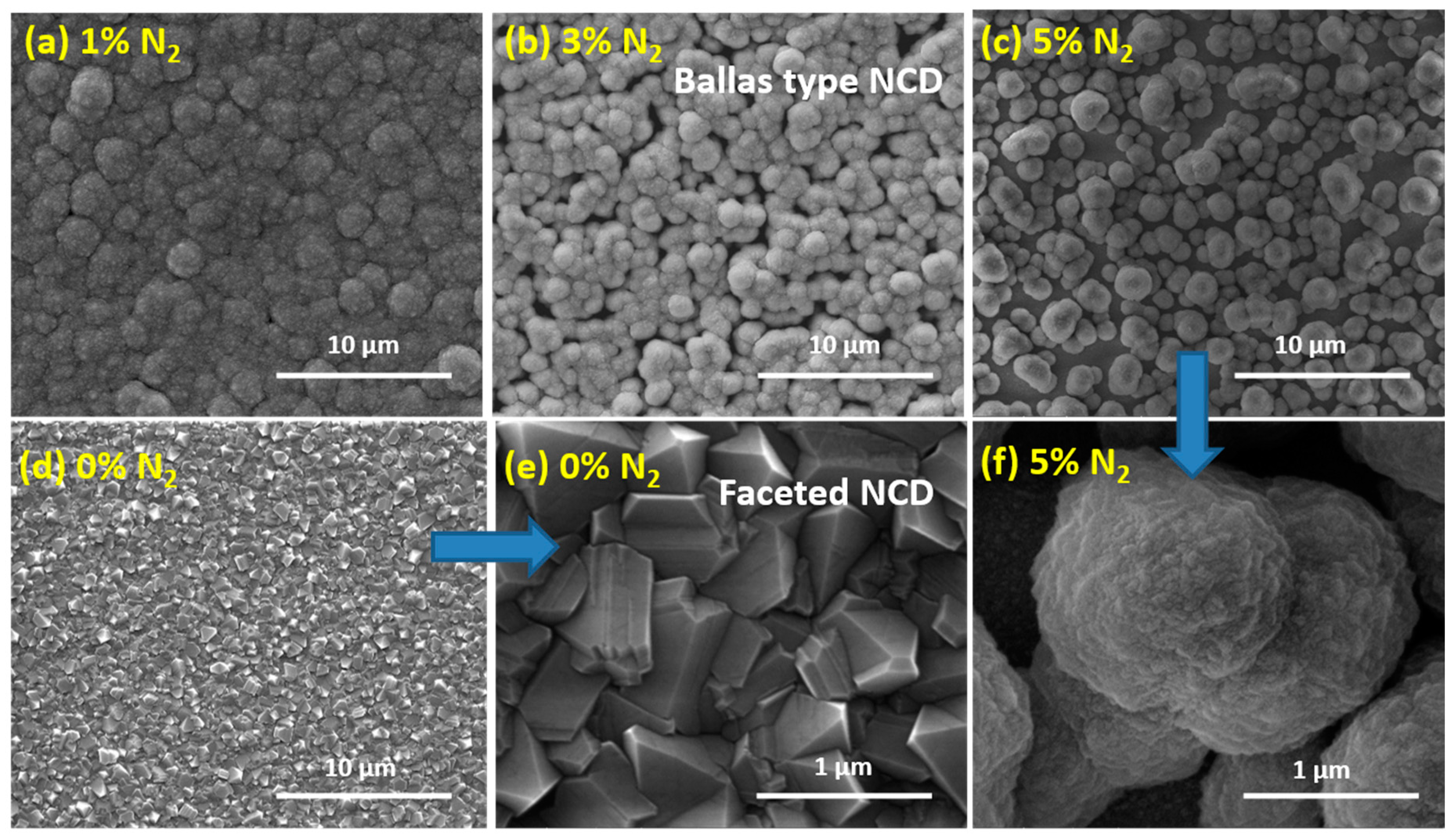
Figure 2.
Morphologies of diamond films, on Si substrates deposited with (a) 1%, (b) 3%, (c) 5% N2, (d) higher magnification SEM image of figure (c), and, on GaN/Sapphire substrates with (e) 3% and (f) 5% N2 in the CVD process gas recipe.
Figure 2.
Morphologies of diamond films, on Si substrates deposited with (a) 1%, (b) 3%, (c) 5% N2, (d) higher magnification SEM image of figure (c), and, on GaN/Sapphire substrates with (e) 3% and (f) 5% N2 in the CVD process gas recipe.
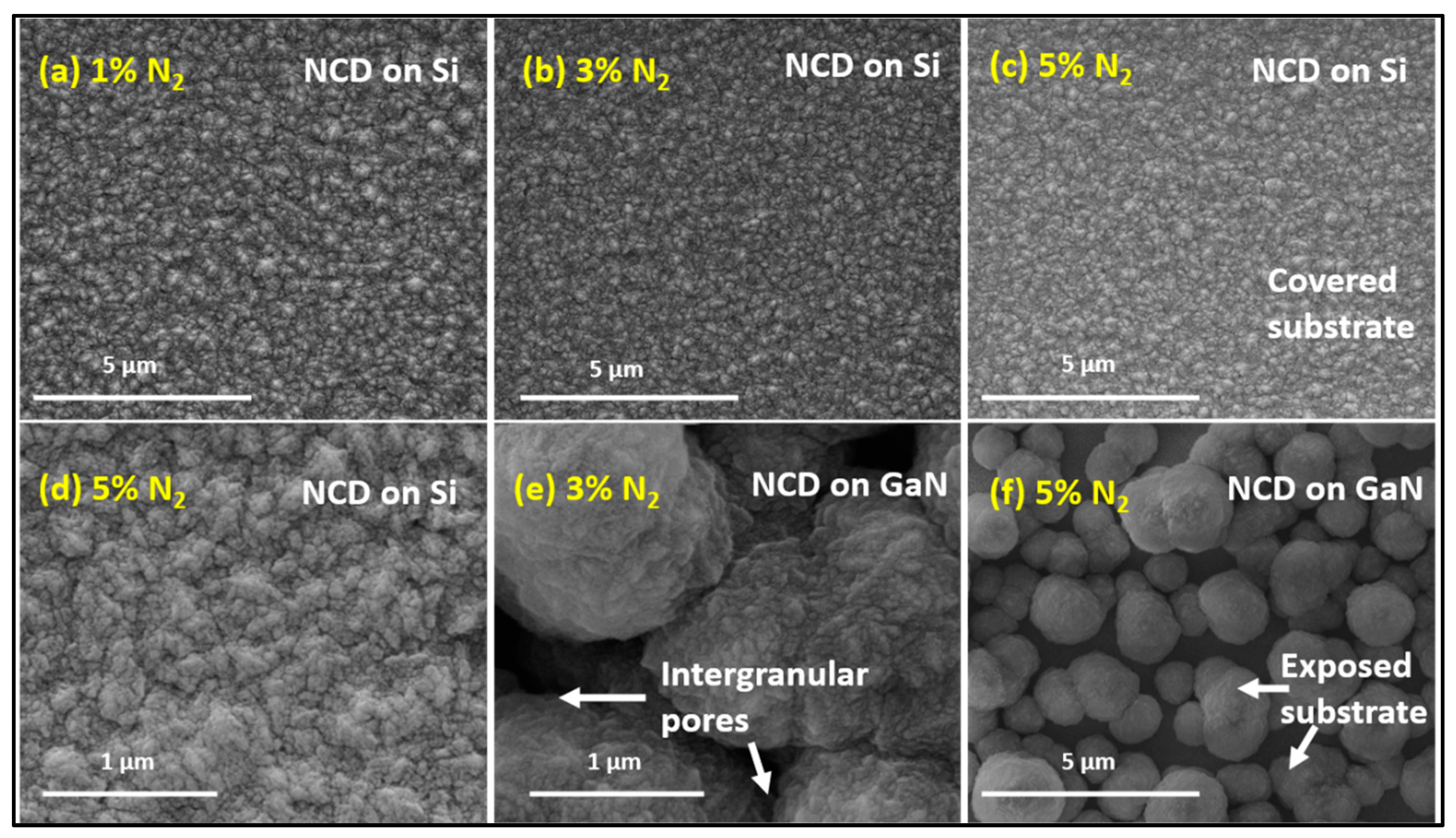
Figure 3.
Energy dispersive X-ray spectroscopy (EDS) of the diamond films on GaN/sapphire substrates deposited with (a) 1%, (b) 3%, (c) 5% and (d) 0% N2 in the CVD process gas recipe.
Figure 3.
Energy dispersive X-ray spectroscopy (EDS) of the diamond films on GaN/sapphire substrates deposited with (a) 1%, (b) 3%, (c) 5% and (d) 0% N2 in the CVD process gas recipe.
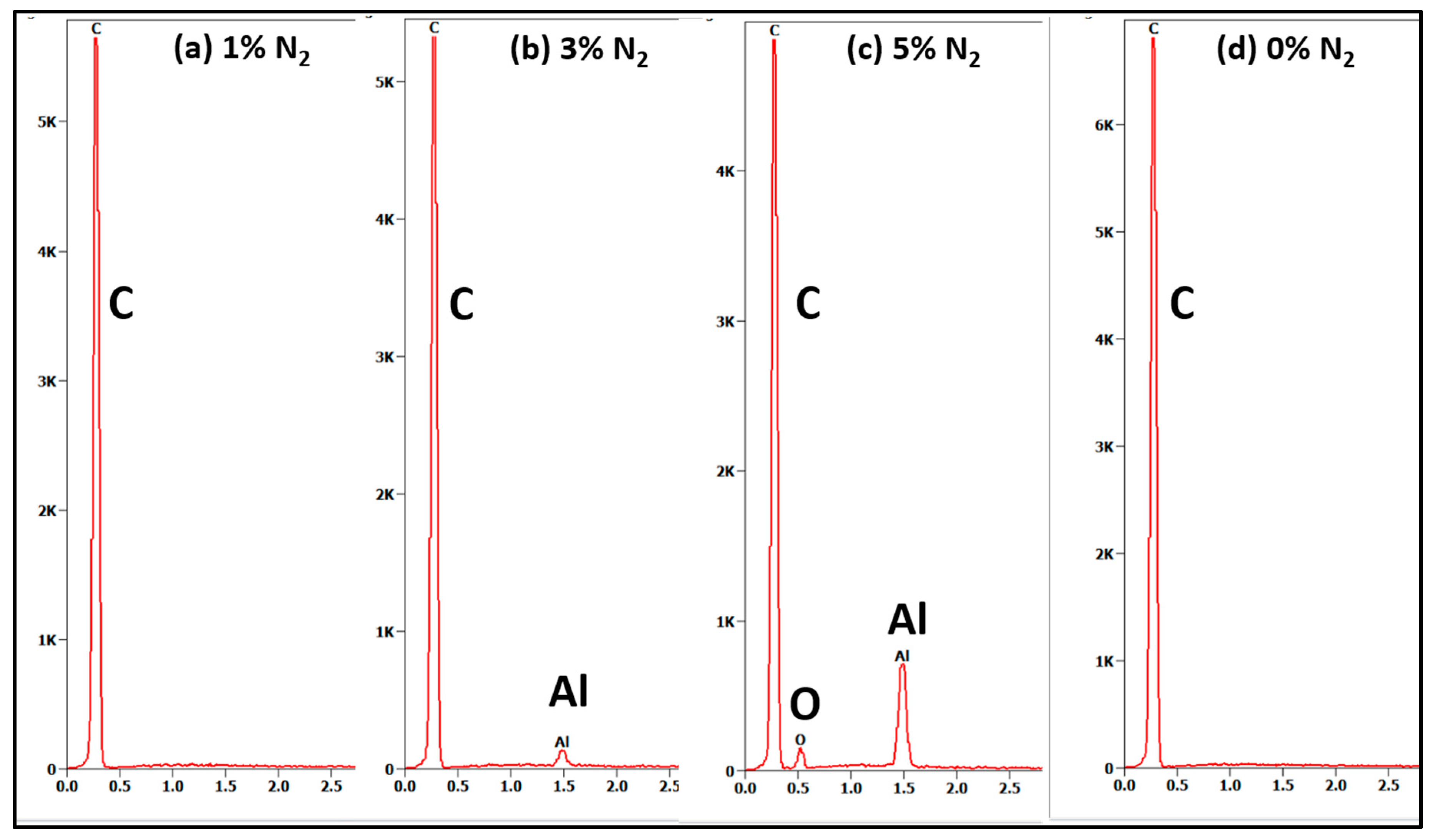
Figure 4.
Raman spectra of the diamond films on GaN/sapphire substrates deposited with (a) 1%, (b) 3%, (c) 5% and (d) 0% N2 in the CVD process gas recipe.
Figure 4.
Raman spectra of the diamond films on GaN/sapphire substrates deposited with (a) 1%, (b) 3%, (c) 5% and (d) 0% N2 in the CVD process gas recipe.
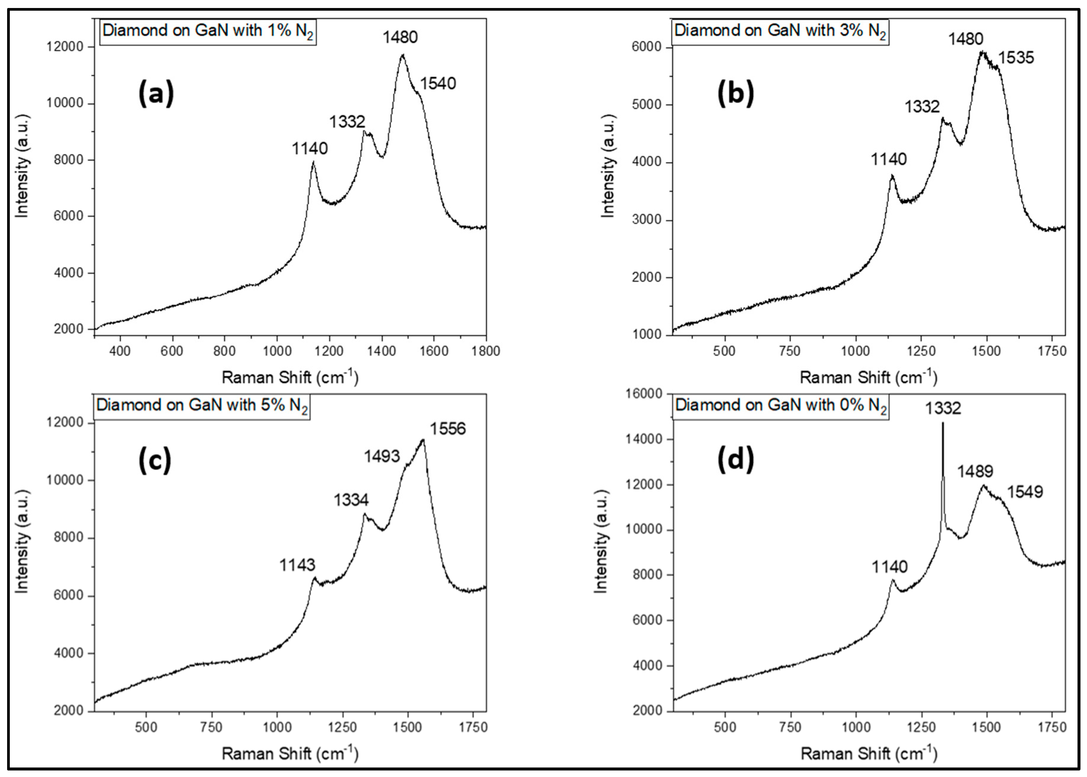
Figure 5.
Fourier transform infrared spectroscopy (FTIR) graphs of the diamond films on GaN/sapphire substrates deposited with (a) 1%, (b) 3%, (c) 5% and (d) 0% N2 in the CVD process gas recipe.
Figure 5.
Fourier transform infrared spectroscopy (FTIR) graphs of the diamond films on GaN/sapphire substrates deposited with (a) 1%, (b) 3%, (c) 5% and (d) 0% N2 in the CVD process gas recipe.
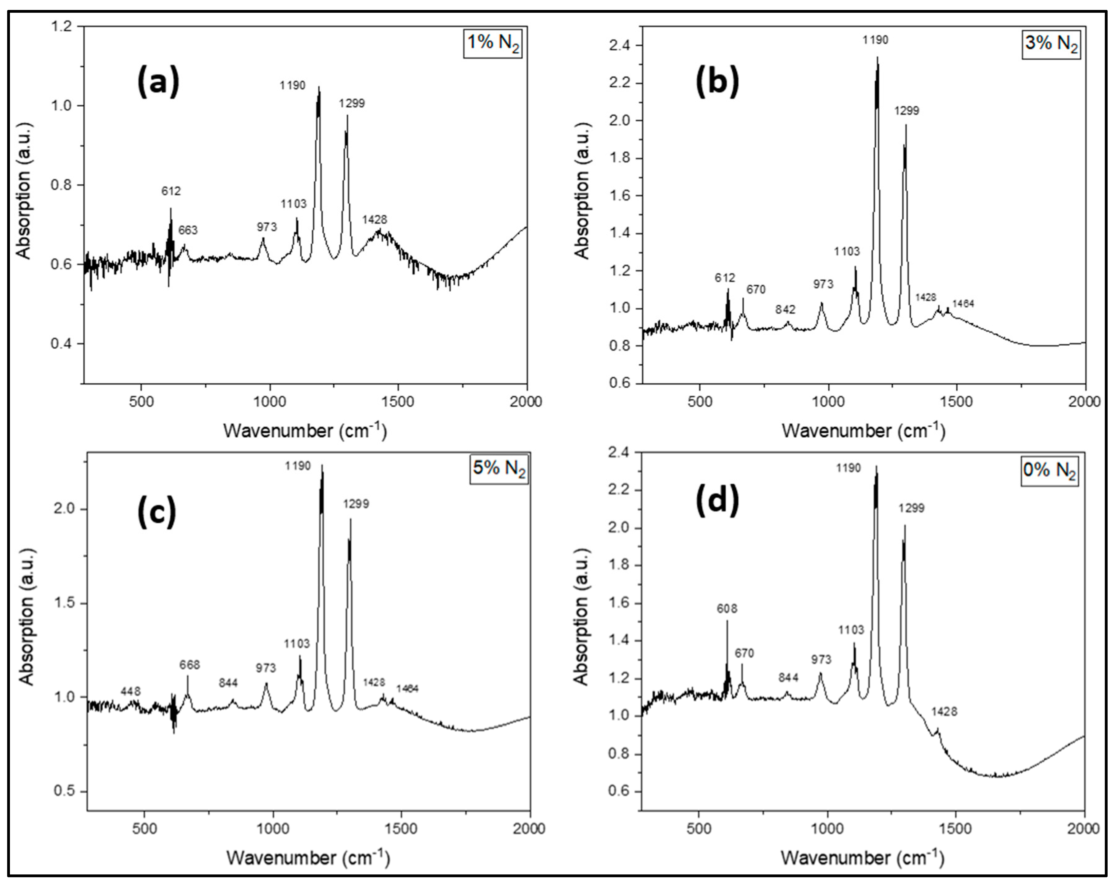
Figure 6.
X-ray diffraction peaks from (a) bare GaN-on-sapphire substrate and, (b) sample #D5.
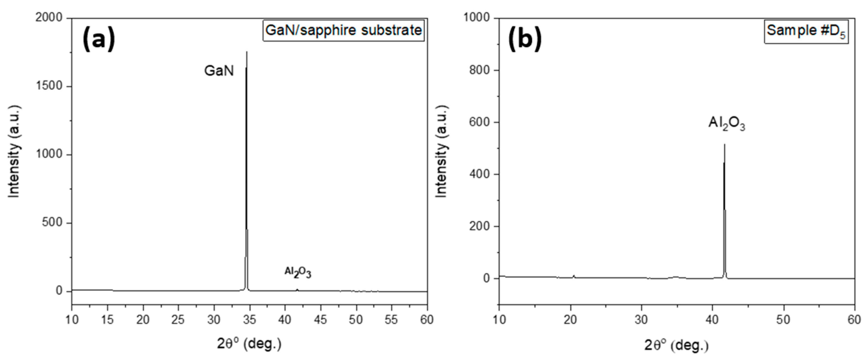

Table 1.
CVD process parameters for growing diamond films on GaN/Sapphire substrates.
| Sample # | N2 (%) |
H2 (%) |
CH4 (%) |
CO2 (%) |
Tsubstrate (oC) |
Power (kW) |
|---|---|---|---|---|---|---|
| D0 | 0 | 94 | 6 | 0 | 600 | 3 |
| D1 | 1 | 93 | 6 | 0 | 600 | 3 |
| D3 | 3 | 91 | 6 | 0 | 600 | 3 |
| D5 | 5 | 89 | 6 | 0 | 600 | 3 |
Table 2.
Experimental evidence of the effect of the N2 gas addition on GaN etching.
| Sample # |
N2 (%) |
Al EDS peak intensity at 1.49 eV (counts) |
Ga-N FTIR peak intensity (a.u.) |
Diamond qualities (Raman peak ratio Isp3 / ID) (%) | Diamond average grain sizes (μm) |
|---|---|---|---|---|---|
| D0 | 0 | absent | 151 | 59 | 0.5 |
| D1 | 1 | absent | 74 | 50 | 2.0 |
| D3 | 3 | 105 | 110 | 50 | 0.9 |
| D5 | 5 | 680 | absent | 50 | 1.0 |
Disclaimer/Publisher’s Note: The statements, opinions and data contained in all publications are solely those of the individual author(s) and contributor(s) and not of MDPI and/or the editor(s). MDPI and/or the editor(s) disclaim responsibility for any injury to people or property resulting from any ideas, methods, instructions or products referred to in the content. |
© 2024 by the authors. Licensee MDPI, Basel, Switzerland. This article is an open access article distributed under the terms and conditions of the Creative Commons Attribution (CC BY) license (https://creativecommons.org/licenses/by/4.0/).
Copyright: This open access article is published under a Creative Commons CC BY 4.0 license, which permit the free download, distribution, and reuse, provided that the author and preprint are cited in any reuse.


