2.2. Data Readout Firmware
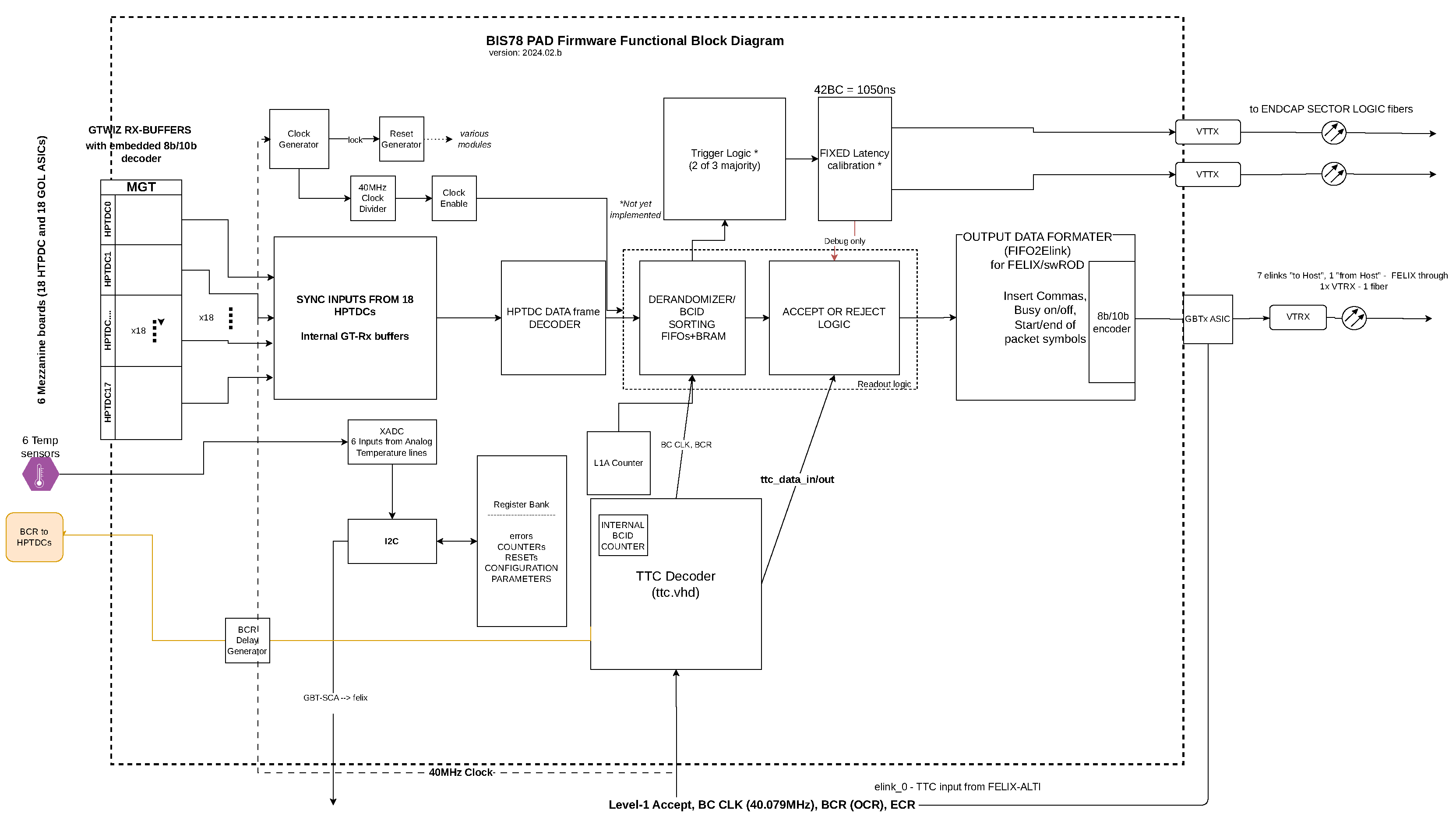
One of the most demanding parts in terms of research and development for this project, after the design of the electronics boards, has been the firmware (FW) (or gateware) for the Kintex-7 FPGA placed on the PAD board. There has been continuous development and improvement since May 2022, when a new firmware project was initiated. As mentioned before, one FPGA performs all the data-readout and, in the future, the trigger functions for one sector, which means up to 576 readout channels. The PAD board takes cares of the digital data acquisition and synchronization, decoding, sorting of the data according to their BCID, selective (triggered) read-back from the storing BRAM and data-formatting in FELIX appropriate format. The Functional Block Diagram displaying all the top level modules is presented in
Figure 5.
For the PAD logic to be working synchronous to the LHC clock (also called TTC clock), two basics components required are the TTC Decoder, which receives and decodes the TTC information from FELIX [
20] to be then internally used, and the Clock generator, which synchronizes all the PAD logic with the TTC clock and/or to other specific clock signals generated from it.
TTC Decoder: The TTC signals are generated by the ALTI module (directly, or inherited by the CTP), decoded inside FELIX and finally transmitted over fiber to the PAD board.
Synchronous to the TTC clock, three important signals are sent by FELIX and used inside the PAD board: the Bunch Counter Reset (BCR), the Event Counter Reset (ECR), and the Level-1 Accept (L1A).
The BCR serves the purpose of resetting the bunch crossing counter, which increments with each clock cycle on the TTC 40 MHz clock. This counter, also known as BCID, is a 12-bit counter. Approximately every 89 s, a BCR command is transmitted, aligning with the time it takes for a bunch to complete a circuit in the LHC. Within this interval, the BCID counter reaches its maximum value of 3564 counts.
The L1A communicates with the detector front-end readout systems, indicating whether to retrieve the event information stored in the front-end electronics pipelines.
The ECR is employed to increment the event reset counter, set to reset every 5 seconds for ATLAS. Combining the event reset counter with the L1A counter results in the Extended L1ID (EVID), a 32-bit value. The lower 24 bits contain the L1A counter, while the upper 8 bits contain the event reset counter. Upon receiving an ECR, the upper counter increases by 1, and the lower part resets to zero. With each L1A reception, the lower part increments by 1.
BCID and EVID values function as labels for the data accepted by the trigger.
A dedicated E-link, named TTC E-link, is used for transmitting the TTC information. The TTC E-link is configurable and, for the BIS78 project, it runs at 320 Mbps, transferring 8 bit TTC information on every TTC clock according to the
Table 1.
The full TTC e-link frame is transmitted from FELIX to the PAD, from the MSB (bit-7) to the LSB (bit-0). Every piece of TTC information is contained within one bit period, which is equivalent to 3.125 ns (the TTC signal runs at 320 MHz).
Clock Generator: Another basic component is the IP-based Clock Generator which is connected to the 40 MHz TTC clock input from FELIX and from which all the necessary clocks are generated.
In order to sample the TTC information, a higher frequency clock is needed. For this purpose, the Clock Generator is used to create a 320 MHz clock. The clock is delayed by 1.5625 ns with respect to the incoming TTC clock, and thus to the TTC stream, in order to correctly decode the TTC incoming data. Since the TTC stream is output with this delay, all the other internal clocks, used to elaborate this information, are delayed by the same time (1.5625 ns) in order to be aligned to it. A delayed version of the 40MHz clock is used for the TTC configuration block, and for the L1A and the EVID counters, whereas a further 40 MHz 180 °C shifted clock is used to send a delayed version of the BCR to the HPTDC. The delay value, which corresponds to 12.5 ns, has been chosen in order to respect the HPTDC specifications.
The Clock Generator generates three extra higher frequency clocks, an 80 MHz, a 160 MHz and a 320 MHz, in phase with the TTC delayed clock. The 80 MHz is used by the de-serializers, whereas the 160 MHz and the 320 MHz are used to speed up the remaining logic (the Readout Logic and Output Data Encoder, respectively). The Clock Generator has a locked signal output, which indicates the component is producing stable and reliable clocks. For this reason, the locked signal is used as an active low reset for all the PAD logic.
Deserializer (GTX) and HPTDC Data Decoder: The HPTDC’s output data frame, which is fed into the GTXs, is illustrated in
Figure 6 This output data frame, consists of 32 bits transmitted every 25 ns (40 MHz rate), containing the following fields: the HPTDC header (the four most significant bits of the frame). Normally, the HPTDC header is set to the constant binary value "0100", which indicates the HPTDC is working without errors in pairing mode. However, if the HPTDC detects an error condition, the HPTDC header is set to the binary value of "0110". Additionally, the frame includes the channel ID (identifying each of the 32 channels read from each HPTDC), the TDC ID (identifying the HPTDC), the hit width and leading time values, and the BCID (Bunch Identifier). As already mentioned, the hits data coming from 18 HPDTCs are serialized and 8B/10B encoded by the GOL ASIC before being transmitted to the PAD at 1.6 Gbps. On the PAD board, 18 GTX Gigabit Transceivers (a commonly used transceiver technology provided by Xilinx) are employed for the de-serialization process. To minimize power consumption, the GTXs are configured with Receiver (Rx) only, as the transmitter part is not used. The internal Rx buffer as well as the 8B/10B decoder are enabled to achieve alignment and synchronization, and to decode input data. Moreover, to reduce latency, the GTXs have been configured to serialize a 16-bit word every 50 ns (80MHz).
The GTX 16-bit parallel words are then processed by the
HPTDC Data Decoder block which, by looking at the 8B/10B comma words (corresponding to the hexadecimal values "50bc" and "c5bc"), is able to correctly align two consecutive words to reconstruct the 32 bit HPTDC frame (
Figure 6). The reformatted 32-bit words are then sent to the next block, the
Readout Logic.
Readout Logic: In the readout block, the input data is stored in two types of FIFOs and a Block RAM (BRAM). The logic can work in two modes: “pass-through”, where all data are sent out, or L1A-information based, which means that only when an L1-Accept signal arrives, data with the appropriate BCID tag are sent to the next block, where it is formatted and transmitted to FELIX via an optical link. In normal ATLAS runs, the L1A signal is issued by the Central Trigger Processor, the CTP. According to the hardware structure described in
Section 2.1.1, the readout logic consists of six replicas of the Readout block, each processing data coming from one mezzanine, i.e. from three HPTDCs.
Three 32-bit TDC-FIFOs are used to store the decoded output data of three HPTDC chips. Then, the HTPDC header of each frame is checked to validate the data (data frame structure in Fig.). If the header is "0100" the data is considered reliable and transferred to an additional TDC-FIFO, common to all the HPTDCs. If the header indicates an error (set to "0110"), the data is discarded, and an error monitor counter is incremented. The DATA-BRAM, 32-bit wide and 8192 locations deep, functions as a derandomizer controlled by the Readout Finite State Machine (FSM). Indeed, the Readout FSM manages writing and reading to/from the DATA-BRAM. It ensures that hits related to the same BCID are stored into consecutive locations within DATA-RAM. Up to 32 possible locations per BCID are available, corresponding to the maximum hit multiplicity expected under normal conditions. The dimensions of the DATA-RAM are chosen to safely store hits belonging to up to 256 BC (i.e. 6400 ns) before they are possibly selected.
In order to select the data with the appropriate BCID tag, very important is the information stored in the 44-bit L1A-FIFO. In the L1A-FIFIO, the L1ID and BCID values at which a L1A signal arrives are stored. Starting from the stored BCID and knowing the L1A signal latency, the Readout FSM calculates the readout BCID, so that it can read from DATA-RAM the data corresponding to the readout BCID up to the next following 6 BCID. The maximum value of BCID to be sent out is selected by the readout window parameter, and it has been chosen to facilitate the calibration of the detector during commissioning.
Output data format: The data formatting is handled by the Readout FSM. The data format shown in
Figure 7. For each L1A signal received, data corresponding to up to 6 consecutive BCID can be sent. This stream consists of a variable number of 16-bit width words, depending on the number of hits and the selected readout window width. The 16-bit width size has been chosen to fit the width constraint of
FIFO2elink module, which is going to be described in the next section.
For each communication to FELIX, via the e-links, two header words (Header_0 and Header_1) are necessary, containing specific FELIX ID identifiers and information, among which the 12-bit readout BCID value plays a fundamental role in the data reconstruction. The next two words contain the 32-bit EVID. The EVID is eventually followed by the HPTDCs data belonging to the readout window, up to the Last_word-2. Two words per each HPTDC data are necessary. The data are followed by a footer block, which starts with the "a0" hexadecimal symbol and contains the information of how many hits per BCID (in the readout window) have been sent. The range is from the first readout BCID called BCID0, up to BCID0+6, which represents the last BCID in the readout window.
The SW ROD plugin, which is custom-made for this project, as done for other ATLAS sub-detectors separately, can be programmed to store the whole data input to it, or discard some parts.
Output Data Encoder (FIFO2elink): From each readout block, the outputted formatted data needs to be sent to FELIX, using one of the available e-links.
The FIFO2elink module is used to encode the data according to the 8B/10B protocol before being sent to FELIX (optical communication over VTRX). The module is part of the ATLAS FELIX Project Firmware, released as open-source in [
11]. The related sources of firmware have been modified as required to fit the needs of the PAD board. The output rate is locked to 320 Mbps per e-link, for a total of 6 data e-links. After being processed by the GBTx ASIC, which is configured to GBT mode, which involves 120-bit wide output frames. A separate e-link for monitoring purposes, is considered for future implementation.
Trigger Logic: At the time of writing this document, this part is under development. Here, the signal is sourced from the Readout, and the data words -selected by L1A-info- are processed based on the 2-out-of-3 majority simple algorithm. Thus when a traversing muon hits one layer, incident within a wide range of angles, also a hit would be expected on one or both the two of the rest layers. If at least two (or all three) layers have a hit, in strips with close proximity between them, this means that the hit is valid. The data that correspond to these hits can be read-out from the Readout FIFOs and BRAM. Eventually, only this trigger information contained in the data words, forms the so called trigger candidates and will be sent via two fibers, using the two VTTX transmitters of the PAD to the End-cap Sector Logic electronics.
One last step remains: to adjust the output data to the End-cap Sector Logic at a fixed latency. This requirement is set by the Experiment’s Trigger sub-system, and should be exactly 42 BCs or 1050 nanoseconds.
Configuration via GBT-SCA and Register Bank: A set of configuration registers, which control FW parameters like BCID offset, TTC offset, Readout mode and more as well as other registers used as counters such as the TTC signals rate counter and the HTPDC error counter, are implemented in the FPGA. During development -before functionality was implemented- most of these parameters and configurations were set or read, by using VIOs in Vivado. For system testing, a C++ tool called I2C_scope is used to execute configuration and monitoring actions over .
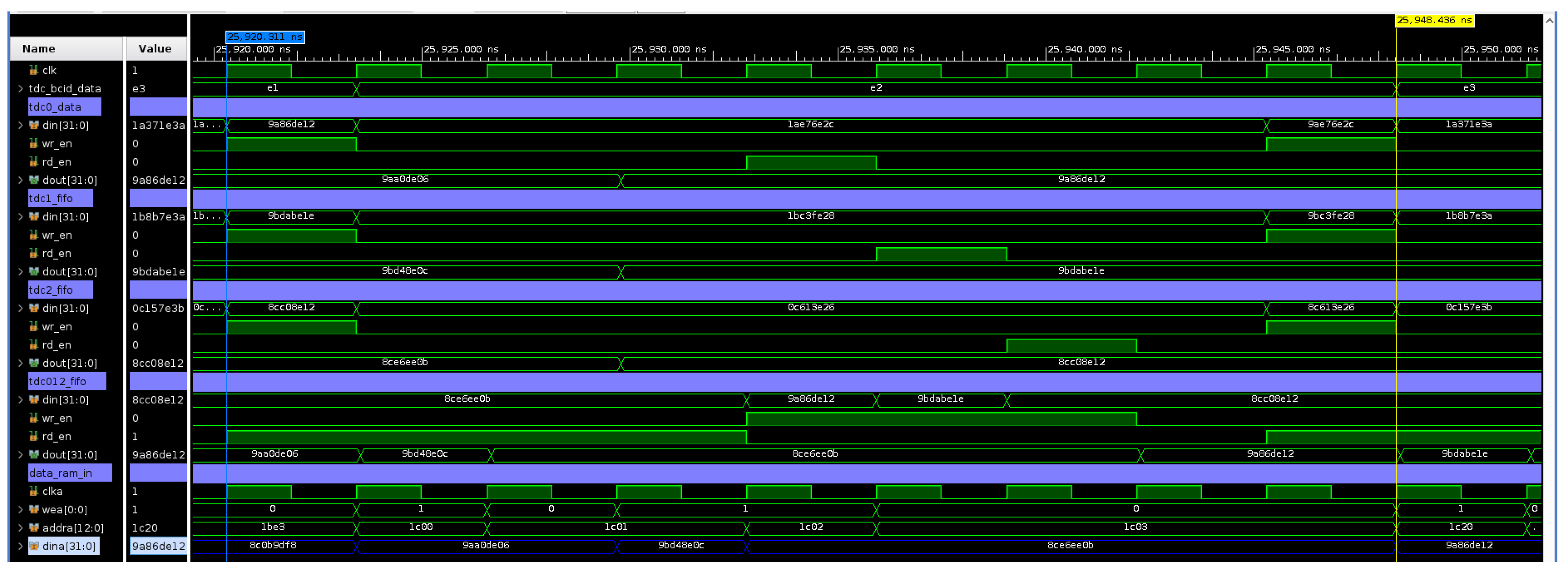
Simulation waveforms are shown in
Figure 8 and
Figure 9. In these Figures, the random inputs corresponding to 3 different HPTDCs are generated. There is one generated input L1A signal. Also the process of writing/reading the data into/out of the FIFOs and the BRAM is shown.
2.2.1. Resource Utilization
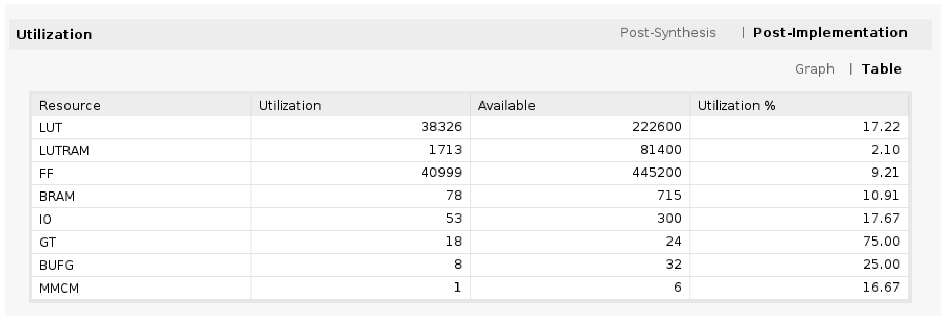
The resources used on the FPGA device are displayed in
Figure 10 as reported by Vivado 2021.2 with the vast majority of the Readout firmware implemented and with minimal ILA usage.
All the values are below 50%, except for the GTX receivers (but their number is final). Also the total On-Chip power reported is 5.494 W. As an indirect comparison, the PAD board which host the FPGA has has a measured consumption of 11.5 W for sector A4 and 12.5 W for sector A14.
