Submitted:
25 April 2024
Posted:
27 April 2024
You are already at the latest version
Abstract
The aim of this research work is to get a method for Galfenol electrodeposition thought which we can control the desired percentage of Ga versus Fe that has the maximum magnetostriction constant. Galfenol is electrodeposited on an optical fiber with an imbedded Fiber Bragg Grating (FBG) in its core. The final objective, that goes further of the scope of this research, is to get an optical magnetostrictive sensor. The device will sense magnetic field or current based on the combination of this magnetostrictive Galfenol, that will stress the optical fiber with the application of magnetic field or current and will change the reflected wavelength of the FBG as a consequence of the variation of the Bragg wavelength. We have developed a method of electrodeposition that allows controlling the density of current in the electrodeposition process in order to get the desired percentage of Ga and Fe in the alloy Ga X Fe 1-x. We have manufactured a set of samples with different parameters (as density of current and pH) and we have characterized these samples morphological, structural and magnetically. With this research we want to give to the scientific community the groundwork to design magnetostrictive optical sensors based on and FBG coated by giant magnetostrictive material. In this paper we have developed a method of covering the optical fiber controlling the composition of (Ga X Fe 1-X) in order to be able to get the maximum magnetostriction constant.
Keywords:
Electrodeposition
; Galfenol
; Optical Fiber
; FBG
; Magnetostriction
1. Introduction
The discovery and utilization of optical fibers have led to substantial advancements in information exchange processes, which continue to evolve today, as well as in the measurement of various magnitudes, as strain and temperature 1. The combination of an optical fiber with and embedded FBG and coated with a magnetostrictive material opens a new field of sensors, as magnetic field sensors and current sensors 2. The adoption of optical fibers has solved numerous issues, including signal loss and noise, that were previously encountered with initial electrical sensors.
To date, the most commonly employed optical sensors are those based on diffraction Bragg gratings (FBG). An FBG have unique characteristics that render it suitable for use as a sensor 1. An FBG is a structure based on a periodic alteration of the refractive index situated within a standard single-mode optical fiber segment, typically reduced to a few millimeters in length. It is distinguished by its periodic, resonant, and spatial attributes. Moreover, it alters the refractive index within the fiber’s core, where multiple interfaces exist between regions with different refractive indices. At each of these interfaces, a portion of the light signal injected in the fiber is reflected (the FBG acts as a selective wavelength optical reflector), while the rest of the wavelength are transmitted. The FBG behaves like an optical filter, reflecting a specific wavelength and transmitting the rest of the spectrum 4. The wavelength at which the maximum reflectivity is produced, is known as the Bragg wavelength.
The Bragg wavelength is given by:
whereis the effective refractive index of the fiber core and is the physical period of the induced refractive index modulation. Under strain or temperature changes, the Bragg wavelength suffers a shift that can be expressed as the sum of the effects of these two contributions 4:
The first term of the relative variation of the Bragg wavelenght represents the strain dependence, where and are the coefficients of the strain-optic tensor, is the Poisson ratio and is the strain. The second term shows the temperature dependence of the relative variation of the Bragg wavelenght, whereis the thermal expansion coefficient of the optical fiber and is the thermal coefficient of the effective refractive index.
FBG offers a wide range of applications, as optical reflectors, optical filters or as an optical device embedded in an optical fiber. FBG-based sensors have gained significant importance in today’s technology 5. FBG are employed in numerous applications, primarily due to the significant advantages they offer 6: they offer reduced insertion loss since they are fabricated within an optical fiber 7, they function as highly selective wavelength filters, they are tunable, both through strain and temperature; in other words, changes in these parameters impact the refractive index and the period of the Bragg grating of the FBG and they are immune to electromagnetic interference. Although these applications are predominantly found in optical communications, the utilization of FBGs in sensing is also widespread. This is attributed to their distinctive characteristics, as they are well-suited for temperature and strain sensing. Consequently, parameters that induce changes in temperature and strain can also be effectively measured with and FBG embedded in an optical fiber, such as strain, pressure, temperature, magnetic field, current, or any other magnitude that can be transduced to a strain or temperature.
One of the most intriguing research areas involving FBG-based sensors is the exploration of magnetostriction. Magnetostriction is a phenomenon observed in ferromagnetic materials, causing them to change its dimensions (strain change) when subjected to a magnetic field. By utilizing key magnetostrictive materials, such as Nickel, Terfenol-D, or Galfenol (which will be extensively discussed in this study), and depositing them on various substrates such as thin films 9, nanowires 13, or cantilevers 15, researchers have gained insights into the behavior of this property. This has led to the discovery of advanced applications in microactuators 17 and cutting-edge sensors, including MEMS devices 18. Research in magnetostrictive sensors based on FBGs and magnetostritive material has been extensive. These sensors are designed for measuring magnetic fields, electric current, and temperature. When a magnetostrictive material like Galfenol or Terfenol-D becomes magnetized, it experiences a deformation that is transmitted to the substrate on which it is applied 2. In the context of this research, the optical fiber with an embedded FBG and coated by a high magnetostrictive material undergoes either stretching or compression alongside the composite material, and this strain of the FBG results in a change in the grating period and, consequently, alters the Bragg wavelength.
The mechanism of magnetostriction at the atomic level is a relatively complex topic. However, it can be divided into two distinct processes at the macroscopic level. The first process involves the deformation of the domain walls within the material in response to external magnetic fields. The second process is the rotation of these domains. These two mechanisms enable the material to alter the orientation of the domains, leading to a change its dimensions. Because this deformation is isometric, there is a corresponding dimensional change in the orthogonal direction 19. While there can be multiple pathways to achieve domain reorientation, the fundamental concept is that the rotation and movement of the magnetic domains result in a physical change or deformation in the material.
2. Galfenol Electrodeposition over an Optical Fiber
In order to get the electrodeposition of Galfenol on the optical fiber we need to do two previous steps; sputtering and chemical deposition. This is because electrodeposition cannot be done on a nonconductive material. In first step we cover the optical fiber by sputtering with a Ni layer of 100nm. In second step, we do chemical deposition on the Ni sputtered optical fiber to get a thicker Ni layer, with lower enough resistivity to do the electrodeposition process.
2.1. Nickel Sputtering
Sputtering is used to coat the FBG with a Ni conductive layer. This is going to turn it into a cathode, which is necessary for the electroplating. The distance between the target and the sample will vary depending on the element to be deposited. In this project, nickel sputtering has been carried out. The conditions applied in the sputtering process are a distance from the fibers to the target of 5 cm and an applied intensity of 90 mA.
In order to achieve the proper results, it must be ensured that the vacuum value is kept below 10-5 mbar. Once the proper vacuum value has been achieved, argon gas is allowed to enter the capsule, maintaining the internal pressure between 2∙10-2 and 5∙10-2 mbar.
In order to achieve a layer thickness of approximately 100nm, the total time of the process was ten minutes (the sputtering was done in two times of 10 minutes each, rotating the fiber 180ο to cover all around the fiber with Ni).
2.2. Nickel Chemical Plating
Nickel sputtering provides a thin layer of nickel (around 100nm), although it is not thick enough to do the electroplating process due to its high resistance. In order to do a constant current electroplating we need to get a lower resistance of the sample. For this reason, electroless nickel plating (chemical plating) is subsequently carried out to achieve a high conductive layer on the sample. This conductive layer will be our electrode.
It is essential to add that it is not possible to do the nickel plating directly on the fiber since the nickel needs other Ni particles to be electroplated (or other metallic surface) [20,21].
Table 1 shows the components and quantities of an aqueous solution of 250mL used in Ni chemical plating. In general, it is important to bear in mind that the mixture must have a pH between 8 and 9 (ammonia has been used to regulate the pH), and the working temperature should be higher than 90ºC 20.
In Figure 3 it is shown a set of SEM and EDX images of an optical fiber covered by Ni and Fe. These images reflect the deposited layers on the optical fiber. Figure 3(a) shows a SEM image of an optical fiber subjected to all the fabrication process, that is, sputtering, chemical plating and electroplating. It can be seen the optical fiber in the center of the wire with a 135 µm diameter. In Figure 3(b) it is shown an EDX image of the Ni layer. This Ni layer has been got by sputtering (100nm) and with chemical deposition (5µm) and the first layer of chemical deposition layer of Ni and the Fe layer by electrodeposition. In Figure 3(c)-(e) are shown the EDX image of the Si and O due to the SiO2 of the optical fiber. In Figure 3(d) is shown the EDX of Fe layer (~30µm thickness, attempt to electroplate GaxFe1-x, but only Fe was deposited as the density of current employed was over 40mA/cm2, with 7mA on an optical fiber of 3.5cm length).
Galfenol Electrodeposition
The objective of the Galfenol electrodeposition on the optical fiber with an FBG embedded inside is to get a magnetostrictive sensor. For that, we pretend to use the giant magnetostrictive properties of Galfenol 23. The magnetostriction constant depends strongly on the percentage of Ga and Fe. In the alloy GaXFe1-x, the highest magnetostriction constant, 3/2 𝜆100, is get at around 18% and 28% of Gallium, being that value around 400 µε 24. in this paper, we are going to referee this Figure 4 in the analysis of the samples, but we have to clarify that it refers to a crystalline sample in a bulk sample, which is substantially different to our samples grown by electrodeposition on amorphous state (we have no reference about the magnetostriction of this kind of samples).
On the other side, the percentage of Ga and Fe by electrodeposition depends on the current density 2526. Conventional methods of electrodeposition are done by applying and electrostatic voltage between electrodes of the electrodeposition cells. In this case, it is used a reference electrode to control de voltage, which fix the percentage between Ga and Fe. The current density depends on the potential between the anode electrode and the reference electrode 28 (for instance, a calomel reference electrode Ag+/AgCl). In Figure 5 it is shown the setup for constant current electroplating, using as anode a Pt wire, as cathode the Ni layer on the optical fiber and the calomel reference electrode. The calomel electrode and measured voltage is used to confirm the relation between voltage and current density. Nevertheless, this relation between voltage and current density follows a very sensible magnitude of current versus potential. Changing the potential between 1V to 1.4V changes the density of current between 3 and 50 mA/cm2 19. That makes very difficult to control the density of current during electrodeposition when using a voltage to control the electrodeposition process.
In this research, we propose a new method of electrodeposition in order to control the density of current. We have used electrodeposition by constant current. That means that instead of using a voltage source to apply to the electrodes of the electrodeposition cells, we have replaced it by a current supply. Whit this, if we know the surface of the sample through which the current flows, we can determine de current density just controlling the current applied to the electrodes and, as a consequence, the percentage of electroplated Gallium and Iron. In Figure 6 it is shown the schematic of the current supply used for the electroplated process. The electronic schema in Figure 6 shows a current source applied to the electrodes, connected in the feedback loop of the operational amplifier. The range of this current supply is between 2 to 15mA. In this first experiment, we have used a constant current supply and we have been changing the level of current as the surface of the sample was growing. Therefore, the current density will not be constant but it will vary little around the expected value.
The first objective of this research is to determine the relation between current density and percentage of Gallium and Iron. This relation will depend also on the pH, the temperature and the current. For that purpose, we have applied a constant current to an optical fiber (first sputtered by Nickel and then with a chemical deposition of Nickel, with the objective of having a conductive Ni layer on with it could be able to do the electrodeposition of Galfenol). As the sample gets electroplated, its surface increases lowering the current density. Whit this procedure, we get the plot of percentage of Ga-Fe versus density of current, with current and pH as parameters. Once we know this relation, we can grow by electrodeposition with a constant density of current, in order to get the desired magnetostriction constant.
3. Magnetic Characterization
3.1. Magnetic Histeresys Loop
The magnetic hysteresis loop represents the nonlinear dependence of the magnetic flux density, B, and the magnetic field, H. A setup system has been developed to obtain the hysteresis loops of the samples (see Figure 8). This system consists of a driving coil, through which an applied current will create the driving magnetic field. Inside the driving coil there are placed two pickup coils. These pickup coils are connected in series-opposition. The sample to be measured will be inside one of the two pickup coils (coil-1). The other pickup coil (coil-2) will compensate the voltage induced in coil-1 due to the magnetic field of the driving coil. As a result, we will get only the induced voltage in the pickup coils due to the magnetization of the sample.
It should be noted that, since only one driving coil is used, special care should be taken to keep the pickup coils within it far enough apart so that they do not interfere with each other and the field can be compensated correctly.
The magnetic field produced by the driving is a function of the number of turns (N) which is the product of the number of turns in one layer (N1) and the number of or layers (N2), the applied current (I) and the length of the coil (l):
We use a copper wire with 1 mm diameter (∅wire). Therefore, we can reformulate the magnetic field:
In case of establishing a maximum current in the driving coil of 14A, the maximum magntic field wil be:
It has been use N2 = 8. Then, the maximum magnetic field will be 112 kA/m. We design the coil with a 14cm length, with a total number of turns of N = 1400 . In Figure 7 there is the schematic of the setup of the coil system for measuring hysteresis loops. In Figure 7 (b),(c) there are the pictures of the driving coils and the pickup coils. The driven coil has been calibrated with a gauss meter in order to get the experimental sensitivity, giving as a result 7.7 kA/m.A.
Once the pickup coil system are assembled, it is necessary to integrate the voltage induced in the pickup coils (e) in order to get the magnetic induction B (the voltage induced in the pickup coils is the derivative of the magnetic flux .
In Figure 8 it is shown the schematic setup and the picture of the system designed to get the hysteresis loop.
4.2. Magnetostriction Measurement with and FBG
Galfenol is a magnetostritive material with a positive magnetostriction coefficient. Due to this magnetostriction effect, when magnetic field is axially applied to the coated FBG, the GaFe coating stresses the FBG and the Bragg wavelength of the FBG suffers a positive wavelength shift. To characterize the composite sensor, the stress of the coated FBG under a uniform axial magnetic field was obtained measuring its Bragg wavelength shift. The driven coil used to generate the magnetic field axially to the FBG has a sensitivity of 7.7 kA/m.A. The coil is connected to a high current programmable power supply (KEPCO BOP 74V-14A). The FBG is connected to an optical interrogator (Micron Optics sm125) to track the Bragg wavelength shift.
Magnetostriction measurement was done by measuring the strain with the FBG embedded in the optical fiber. To provoke the magnetostriction, it was use a triangular magnetic field signal to analyse the linearity of the magnetostriction versus magnetic field, and with a square magnetic field signal to get the maximum magnetostriction for a given magnetic field.
The relation between wavelength shift and strain is 1pm = 1.1µε for the FBG used.
4. Sample Making and Morphological, Structural and Magnetic Characterisation
We have carried out a large number of experimental electrodepositions of Galfenol on an optical fiber. With that, our goal is to get conclusions about the relation of percentage of Ga-Fe and the density of current applied in the electrodeposition process. In this analysis, we have also considered all other parameters that can affect the electrodeposition process, as temperature or pH.
Following, we make a description of same of the manufactured samples, with conditions to electrodeposition, morphological, structural and magnetic characterization and conclusions.
4.1. Sample 1
In the fabrication process of the sample, first, we take out the cladding of the optical fiber. With this, we get the optical fiber with 135μm in diameter of SiO2, with a core of 10 µm diameter, trough where it travels the light. Then we cover the optical fiber by a sputtering process with nickel, with layer of around 100nm thickness. This sputtering process is necessary to get a conductive layer on the optical fiber in order to be able to apply the chemical deposition. Once we get the 100nm Ni layer we do chemical deposition of Ni. The objective of this new layer is to get a conductive layer of Ni with a low resistivity enough to do the electrodeposition. This chemical layer of Ni is grown with a thickness between 5 to 10 μm, which gives a low resistance layer that allows as to apply electrodeposition with currents between 1 to 20mA and with low voltage applied to the electrodes (below 15V, as we connect the electrodes of the electrodeposition bath between output and input of the Operational Amplifier, as a feedback device). The manufacture parameters of sample 1 can be seen in Table 3. Sample 1 have been produced at pH 2,5, with a constant current of I=3mA. The length of the fiber being coated by Galfenol is l=3.5cm. This current gives an initial density of current of δ=19.9mA/cm2. The electrodeposition process has been applied during t=12h getting an average deposition velocity of v=0,6μm/h. We have grown a layer of 7μm of Galfenol and, after the EDX, we have verified that 24% of Ga is present in this alloy (as can be seen in Table 4). In Figure 9, it can be seen the spectrum lines of the EDX with the amounts of Ga and Fe.
In Figure 10(a) it is shown a SEM image of the sample 1, where it can be seen the optical fiber covered by a 7µm thickness of FeGa (24% of Ga and 76% Fe, measured by EDX). In Figure 10(b) it can be observed the Galfenol layer on the optical fiber. It can be seen a Ni layer of 1µm thickness deposited by chemical deposition between Galfenol and the optical fiber.
Sample 1 have and embedded FBG in the core of the optical fiber and we have measured the magnetostriction trough the measurement of the wavelength shift of the FBG due to the strain caused by the applied magnetic field to the magnetostrictive Galfenol layer. In Figure 11 it can be seen the magnetostriction measured with the change in wavelength of the FBG. We get a maximum variation of around 4 pm. It has to be considered that the thickness of the Galfenol layer is only 7μm in contrast with the 135μm thickness of the optical fiber. An unipolar triangular signal of 6A amplitude, which corresponds to a 92 kA/m magnetic field amplitude has been applied axially to the sample. The saturation magnetostriction has been achieved at 1A amplitude, which corresponds to a 7,7 kA/m magnetic field amplitude. As it will be seen in other samples, the hysteresis loop as almost a square shape, with a very high remanence. That means that, the samples are almost magnetically saturated in the axial direction and the increase of magnetization in the axial direction is very small when an axial magnetic field is applied. In order to get the higher magnetostriction the magnetization of the sample has to be orthogonal to the axial direction, being the best magnetic configuration a circular magnetization.
After several samples that we grow with this similar parameter we realize that it is not adequate to use such a low pH. With a pH around 2.5 the deposition velocity is very slow and the solution is so acid that on some proves the solution corroded the previous electrodeposited amount of alloy. Due to such a critical parameter, we decided to grow samples with a higher pH that do not corrode the samples.
3.3. Sample 2
In Table 5 there are the growing manufacture paramenters os sample 5. The core of this sample is an optical fiber of 135 µm diameter. It was grown with a I = 4mA constant current during 92 hours (at an average deposition rate of 2.3 µm/h). The grown was from 135µm to 430 µm in diameter. In Table 5 it can be shown the initial and final parameters in the fabrication process. During the fabrication process it has been controlled the pH keeping it around 4.4, adding ammonia, if necessary, to stabilize the pH. All samples have been produced at room temperature. The chemical deposition takes place at 95 ºC and the electrodeposition at room temperature of 24ºC (the heating by the electrodeposition current is neglected respect to room temperature).
Once the sample has been grown, it is analyzed by SEM and EDX. We measured at different radius the percentage Ga-Fe by EDX (Dispersive X-Rays Spectroscopy). At each radius we get the surface, in order to get the current density, δ = I/S, being r the radius of the sample and l its length.
In Figure 12 (a) it is shown a SEM image of sample 2, with a thickness of Galfenol of 126μm and if Figure 12 (b) it is shown the Ni layer of 3.5 µm grown by chemical deposition over the sputtering layer of 100nm coating the optical fiber.
In Figure 13 (a) it can be seen that the current density diminishes with the growth of the sample (at a constant current of 4 mA), in plot (b) it is shown the Gallium percentage versus the current density measured by EDX. As it can be seen in this plot, the maximum percentage of Gallium is gotten at 12.5 mA/cm2 of current density. This have been done at pH 4.2, which is a very important parameter. From Figure 13 (b) we can see that the density of current has to be below 17 mA/cm2 to get a percentage of Ga over 15%, that according to Figure 4, the alloy starts to have a high magnetostriction constant.
In Figure 14 (a) and (b) it is shown the SEM image of sample 2. It has an inner optical fiber of 135μm in diameter and an outer Galfenol shell of 128μm thickness. In Figure 14 (c), (e) it can be seen the EDX images corresponding to the percentage of Ga and Fe. It fits with the plot in Figure 13(b) where in the outer shell the current density is lower, giving a maximum of Gallium percentage of 23,5% at a current density of 12,5 mA/cm2. In Figure 14 (e) it can be seen that the density of gallium increase as the radius increases (the density of green points increases with radius).
It can be seen that with 12,5 mA/cm2 and pH 4.2 it is obtained around Ga (23%) and Fe (77%), value that is the local minimum of Figure 4 19, which in a crystalline Galfenol could give around 300 µε 31. The samples produced by sputtering, chemical deposition and electrodeposition are amorphous, so the magnetostriction constant will not be the one in the Figure 4, but the proposal in this research work is, once the sample is produced, to crystalize the sample in order to get the proper magnetic domain structure to get the maximum magnetostriction constant in the axial direction of the optical fiber. For that, it is also very important to have the magnetization orthogonal to the axial direction, that is, to have a circular magnetization around the optical fiber (easier than to have transversal magnetization in a circular magnetic sample).
Next step consists in getting the hysteresis loop with the setup described in section 4.1. A signal proportional to the driven current is get by the voltage on a low resistance (0,5Ω) in series with the driven coil and the current power supply (orange signal on Figure 15). The voltage in the pickup coils is plot in Figure 15(a) in blue. This voltage needs to be integrated to get a signal proportional to the magnetic induction (blue signal in Figure 15(b)). The plot in XY mode of both signals of Figure 15(b) gives the hysteresis loop, as seen in Figure 16.
In Figure 16 there are the hysteresis loops of sample 2 for three frequencies; 14Hz (a), 28Hz (b) and 43Hz (c). It can be seen that as higher the frequency higher the coercive field. We can see from these plots that the sample have a high remanence that tells us that the magnetization is almost axial to the wire length. That is the reason why it is gotten a very small magnetostriction of 8pm in wavelength shift (8,8 µε in strain), as can be seen in Figure 17 (b). Magnetostriction has been measured applying a unipolar square driven current signal of 70kA/m to magnetically saturate the sample and measuring the wavelength shift in the FBG.
Figure 17(a) is an optical image of sample 2 where can be seen the Galfenol layer electroplated on the optical fiber.
3.3. Sample 3
Sample 3 was grown with 2.5mA during 48 hours, at an average deposition rate of 4.1µm/h and with 7.5 mA current during the next 48 h, at an average deposition rate of 4.8µm/h. The grown was from 135µm to 1000 µm in diameter. In Table 6 it can be seen the initial and final parameters in the fabrication process. During the fabrication process it has been controlled the pH keeping it around 3.9 in the first stretch to 540µm and them at pH 4.4 for the stretch up to 1000 µm. The pH was controlled by adding the appropriate amount of ammonia. The chemical deposition takes place at 95 ºC and the electrodeposition at room temperature of 24ºC.
Once the sample has been grown, it is analyzed by SEM and EDX. From the analysis of EDX we have get the percentage between Ga and Fe at a different radius form the center of the optical fiber. It has been determined the current density which depends on the current and on the radius (that is, on the surface). With all these measurements and calculations, we have plotted the relation between radius and current density, Figure 18(a), and the Gallium percentage versus radius, Figure 18 (b). Finally, on Figure 18 (c) it can be seen the percentage of Ga versus current density. Due that current density diminishes with the growth of the sample (with a constant current of 2.5 mA), at a radius of 270 µm it was changed the current to 7.5mA to increase the current density. As it can be seen in theses Figure 18 (c), the maximum percentage of Gallium is get around 15mA/cm2 of current density for pH 4.5 and at 7 mA/cm2 for pH 3.9. According to this data we conclude that we have to grow the samples with a pH over 4.5, as with lower pH only at lower current densities it can be obtained a high percentage of Ga and for a specific current density. On the other side, with pH 4.5 an over it is getting a high percentage of Ga over a wide range of current densities, as can be seen in Figure 18(c) in the range from 13 to 18 mA/cm2 with a percentage of Ga between 24 and 32%.
In Figure 19(a) it can be seen a SEM image of sample 3. It can be seen that the sample is rather rough at is surface. As will be deduced with the analysis of all samples, the pH has to be higher in order to get a higher percentage of gallium and a smooth surface. In Figure 19(b,c) there are the EDX images showing the amount of Fe and Ga, with the marked points where the EDX analysis have been done.
3.4. Sample 4
Sample 4 was grown with 2.5mA during 48 hours, at an average deposition rate of 5 µm/h and with 12.5 mA current during the next 48 h, at an average deposition rate of 4 µm/h. The grown was from 135µm to 1017 µm in diameter. In Table 7 it can be shown the initial and final parameters in the fabrication process. During the fabrication process it has been controlled the pH keeping it around 5,9. The pH was controlled by adding the appropriate amount of ammonia. The chemical deposition takes place at 95 ºC during 5 minutes and the electrodeposition at room temperature of 24ºC.
In Figure 20(a) it is shown the current density versus radius. In Figure 20(b) there is the percentage of gallium versus the radius. Figure 20(c) shows the percentage of gallium versus current density. It can be seen that there is a small change of percentage of gallium for the two different currents, but with similar current density. Al higher current densities there are strong changes of percentage of gallium. According to that, for a pH close to 6 it is gotten a lower percentage of gallium, around 10%, but with small variations changing the density of current.
With the analysis of the data, we can conclude that when the pH is increased close to pH 6, the chemical solution reduces its conductivity and the electrodeposition velocity is reduced. As can be seen in the SEM images, when the pH is increased, also improves the quality of the electrodeposition with a more uniform, cylindrical and with a smooth surface of the electroplated wire. On the negative side of increasing the pH, there is the fact, as can be seen in Figure 20 (c), that the percentage of Gallium is reduced below the level that allows us to get the maximum magnetostriction constant (see Figure 4). As can be seen in Figure 21(a), the SEM image of sample 4 shows a smooth surface and cylindrical shape. From the EDX of Figure 21 (b) and (c) it is determined the percentage of Ga and Fe, giving a lower percentage of Ga compared with the samples grown at pH 4.5.
3.5. Sample 5
Sample 5 has been grown with 3mA during 48 hours, at an average deposition rate of 2.5 µm/h and with 4.5 mA current during the next 48 h, at an average deposition rate of 1.6µm/h. The grown was from 135µm to 536 µm in diameter. In Table 8 it can be seen the initial and final parameters in the fabrication process. During the fabrication process, it has been controlled the pH keeping it around pH 4 up to a radius of 192µm and at pH 4.5 up to a radius of 268 µm. From figures 18 (b) and (c) it can be concluded that the pH has to be over 4.5 to get a percentage of Ga over 20%.
In Figure 22 (c) it can be seen the important effect of the pH level on the percentage of Gallium. We can see that at around 14 mA/cm2 current density, the percentage of Gallium increases from 13 to 17% as the pH increases from 4 to 4.5. If a percentage of gallium optimal for the maximum magnetostrictive effect is desired (that is, 18% or 28% of gallium) it will be necessary to grow the sample with a pH of 4.5 or over. We can also see that the tendency of the percentage of gallium could not be the same for different pH levels, as can be seen in Figure 22 (c) between 11 and 12 mA/cm2 of current density. In Figure 23 it can be seen a SEM image of a perpendicular cut of the electroplated wire with the optical fiber at the center and coated by a Galfenol layer of thickness of 200μm.
3.6. Sample 6
Sample 6 has been grown with 3mA during 48 hours, at an average deposition rate of 2.1µm/h and with 4.5 mA current during the next 48 h, at an average deposition rate of 3.8µm/h. The grown was from 135µm to 703µm in diameter. In Table 9 it can be shown the initial and final parameters in the fabrication process. During the fabrication process, it has been controlled the pH keeping it around pH 4.5 as we have concluded that the optimal pH for growing the samples is between 4.5 and pH 5.
In Figure 24, there are the graphs of current density (b) and percentage of Ga (c) versus radius, and in (d) the percentage of Ga versus current density. From the analysis of these plots, it can be seen that we have to use a density of current over 16mA/cm2. It can also be seen that with different current but same current density and pH we get the same percentage of Ga. In Figure 24(a) there is the SEM image of sample 6. The difficulty to cut the sample in its section produces breaks in the sample giving this irregular cut.
With the analysis of all the six previous samples, we can conclude that we have to use an electrolyte solution that have a pH level between 4.5 and 5. With this pH level, we can get a percentage of Ga around 18% or 28%, which are the values that gives the higher magnetostriction constant 19. In addition, we conclude that we have to use a current density over 16mA/cm2 to have a percentage of Ga around 28, which gives a maximum magnetostriction constant according to Figure 4.
3.7. Sample 7
Sample 7 has been grown with 3mA during 48 hours, at an average deposition rate of 1.4µm/h and with 4.5 mA current during the next 48 h, at an average deposition rate of 2.9µm/h. The grown was from 135µm to 554µm in diameter. In Table 10 it is shown the initial and final parameters in the fabrication process. During the fabrication process it has been controlled the pH keeping it around pH 5. By the analysis of previous samples, we can conclude that the deposition velocity is reduced when the pH is increased and that the percentage of Gallium is increased when the pH increases.
In Figure 25 are shown the plots of current density and percentage of Ga. We can see in Figure 25 (c) that the percentage of Ga is higher with a lower current density. We get a maximum of percentage of Ga between 10 to 12 mA/cm2, although the maximum magnetostriction constant is around 28% of Ga, which is between 13 to 18mA/cm2 with the growing current of 4.5mA, but we can see that with the same current density but different current, we get different percentage of Ga. In Figure 26(a) it can be seen a SEM image of sample 7, showing and uniform and smooth surface. In Figure 26 we can see images of sample 6 (b) and sample 7 (c) taken by optical microscope, where can be seen that sample 7, grown with pH 5 has a more uniform surface than sample 6 grown with pH 4.5. With this analysis and the one of previous samples, we conclude that the recommended conditions for growing the sample are 4.5mA and a pH 5.
3.8. Sample 8
Sample 8 has been grown with 5mA during 48 hours, at an average deposition rate of 1.9µm/h. The grown was from 145µm to 330µm in diameter. In Table 11 it is shown the parameters in the fabrication process. During the fabrication process, it has been controlled the pH keeping it around pH 5. By the analysis of previous samples, we can conclude that the deposition velocity is reduced when the pH is increased and that the percentage of Gallium is increased when the pH increases. From the analysis of sample 7 we conclude that it is preferable a current over 4.5mA, so we manufacture sample 8 with 5mA.
In Figure 27 we can see the plots of (a) current density versus radius, (b) Ga percentage versus radius, (c) Ga percentage versus current density. From this data, we can conclude that the increase of the current to 5mA and the pH 4.7 gives a percentage of Ga between 20 and 28% for all the range of current density between 14 to 28 mA/cm2.
In Figure 28 (a) it is shown a SEM image of sample 8. We have measured the magnetostriction of this sample, shown on Figure 24 (b), giving a maximum magnetostriction constant of 9 pm measured with the wavelength shift of the FBG, which corresponds to a strain of 9.9με, as for these optical fibers (1pm corresponds to 1.1 με). The magnetostriction value is very small because the magnetization must be almost saturated in the axial direction. To have a high magnetostriction, the magnetization has to be perpendicular to the direction of the applied magnetic field. Magnetization has to be circular instead of axial (as will be seen in sample 10. To get higher magnetostriction it is necessary to look for a method to rotate the magnetization in the circular direction of the optical fiber).
3.9. Sample 9
Sample 9 was grown on an optical fiber without embedded FBG (so, magnetostriction cannot be measured). Sample 9 has been grown with 6mA for 72 hours, at an average deposition rate of 2.5µm/h. The grown was from 142µm after chemical deposition to 504µm in diameter. In Table 12 it is shown the parameters in the fabrication process. During the fabrication process, it has been controlled the pH keeping it at pH 4.5. We have increased the current in order to increase the current density and the deposition rate. It can be seen in Figure 29 (c) that to increase the current density over 18mA/cm2 reduces the Ga percentage down to 14%, but there is an increase to 22% Ga for a current density of 29mA/cm2. This behavior is quite consistent with the growing parameters of sample 8, where it can be seen in Figure 27 (c) the same kind of behavior as in Figure 29 (c).
The hysteresis loop of sample 9 has been measured. In Figure 30 (a) there is the plot of the hysteresis loop of the sample as cast. It can be seen that the magnetization has a lower remanence than the previous samples. It can be due to the higher electrodeposition current. Reduction in remanence can be caused by the circular magnetic field in the Galfenol layer, caused by the axial electrodeposition current. This creates a circular magnetization that reduces the remanence in the axial direction of the Galfenol coated optical fiber. We have made a temperature annealing process with a current of 400mA passing through the Galfenol layer for 30 minutes. This current produces a circular magnetic field in the Galfenol coated optical fiber, while heats the sample around 350ºC. With this process, we pretend to rotate the magnetization in the Galfenol in order to get a circular magnetization. In Figure 30 (b) it is shown the hysteresis loop after the current and temperature annealing, giving a lower remanence and a more transversal magnetic field (circular magnetization due to the geometry of the sample).
5. Results and Conclusions
In this research work, we have grown composite samples composed of an optical fiber with an FBG imbedded in its core and an electrodeposition of Galfenol coating the fiber. The final objective is to get the experimental data on the optimal parameters to grow the Galfenol. To do these processes, first we had to do sputtering on the optical fiber to get a Ni layer coating the optical fiber. This layer needs to be over 100nm in order to do the next step in the fabrication process. After that, we do electrochemical deposition of Ni. With this procedure, we obtain a thicker layer of Ni between 5 to 10μm. This layer has a resistance lower enough to do the next fabrication step, that is, Galfenol electrodeposition. For the electrodeposition of Galfenol we have developed a new method, doing the electrodeposition at a constant current instead of constant voltage. The reason is that there is a relation between the density of current during electrodeposition and the percentage of Gallium in the Galfenol alloy (Ga X Fe 1-X). The way to control the percentage of Gallium is to control the density of current during the electrodeposition process. The aim of this study is to get the relation between density of current and percentage of Gallium. However, in the electrodeposition process, there are more parameters that affects this relation, those are the current, pH and the temperature. We have made this study at room temperature of 24ºC and we have analyzed as parameters, the current and the pH. We have produced 9 different samples and we have analyzed the results obtained with these samples. As a result, we can conclude that one of the most important parameters is the pH. We conclude that the desired pH is between 4,5 and 5, as we get a smooth surface of the sample and percentages of Gallium that cover the desired value. The desired values of percentage of Gallium are 18 and 28% (according to Figure 4, for a bulk crystalline sample), as those are the values that gives higher magnetostriction constant. After the analysis of all these samples, we have measured the hysteresis loop and the magnetostriction of the samples that had and embedded FGB. Due to the big number of samples that we have produced and analyzed for this study, from which we present only a selection, many of the samples where optical fiber without and embedded FBG. That is the reason that only some samples have these measurements of hysteresis loop and magnetostriction. This is just an initial research to give information to the community that wants to advance in this very interesting research matter, with the final objective of producing optical-magnetostrictive sensors, which can have application in measuring magnetic field and current. With the hysteresis loops, we have noted that the magnetization is axial to the optical fiber. That means that the magnetostriction constant is going to be very low, as the Galfenol electroplated layer is almost magnetically saturated in the axial direction of the optical fiber. When a magnetic field is applied in the axial direction, the rotation of magnetization to saturation is very small, giving a very small magnetostriction constant. To get a higher magnetostriction we need to rotate the magnetization in the perpendicular direction of the optical fiber. The favorable direction of magnetization in this geometry is a circular magnetization around the optical fiber. We have done this in sample 9, getting circular magnetization by applying a high current of 400mA thought the sample, increasing the temperature to around 350ºC, during 30 minutes. With this process we get the hysteresis loop of a wire with almost circular magnetization (couldn’t get magnetostriction of this sample had not an embedded FBG).
We think that with this study we open a new line of research giving the basics of this new electrodeposition method by constant current and the first data of the importance of the fabrication parameters as pH and density of current. Next step to grow a sample with a constant density of current across the diameter of the sample would be to use a current function that makes increase the current as the electrodeposition increases the diameter of the sample.
References
- Thomas, AP. ; Gibbs, MRJ. ; Vincent, JH.; Rithcie, SJ. Technical magnetostriction parameterrs for application of metallic glasses. 1991, IEEE Trans. Mag. 27, 5247. [Google Scholar]
- García-Miquel, H.; Barrera, D.; Amat, R.; Kurlyandskaya, G.V.; Sales, S. Magnetic actuator based on giant magnetostrictive material Terfenol-D with strain and temperature monitoring using FBG optical sensor. Measurement 2016, 80, 201–206. [Google Scholar] [CrossRef]
- García-Miquel, H.; Cebrián, L.; Madrigal, J.; Sales, S. Current Sensor Based on a Fiber Bragg Grating Coated by Electroplated Magnetostrictive Material. IEEE SENSORS 2020, 1–4. [Google Scholar] [CrossRef]
- Grattan, K.; Sun, T. Sens. Fiber optic sensor technology: An overview. Sens. Actuators A Phys. 2000, 82, 40–61. [Google Scholar] [CrossRef]
- Quintero, S.M.M.; Braga, A.M.B.; Weber, H.I.; Bruno, A.C.; Araújo, J.F.D.F. A Magnetostrictive Composite-Fiber Bragg Grating Sensor. Sensors 2010, 10, 8119–8128. [Google Scholar] [CrossRef] [PubMed]
- Ricchiuti, AL.; Hervás, J. ; Barrera, D; Sales, S; Capmany, J. Microwave Photonics Filtering Technique for Interrogating a VeryWeak Fiber Bragg Grating Cascade Sensor. IEEE Photonics Journal 2014, 6, 1–10. [Google Scholar] [CrossRef]
- Barrera, D.; Finazzi, V.; Villatoro, J.; Sales, S.; Pruneri, V. Packaged Optical Sensors Based on Regenerated Fiber Bragg Gratings for High Temperature Applications. IEEE Sensors J. 2012, 107–112. [Google Scholar] [CrossRef]
- Amat, R.; García-Miquel, H.; Barrera, D.; Kurlyandskaya, GV.; Sales, S. Magneto-Optical Sensor Based on Fiber Bragg Gratings and a Magnetostrictive. Materials 2015, 644, 232–235. [Google Scholar] [CrossRef]
- Cao, DR.; Wang, ZK.; Pan, LN.; Feng, HM.; Cheng, XH.; Zhu, ZT.; Wang, JB.; Liu, QF.; Han, GL. Controllable magnetic and magnetostrictive properties of FeGa films electrodeposited on curvature substrates. Applied Physics A 2016, 122. [Google Scholar] [CrossRef]
- Ranchal, R.; Fin, S.; Bisero, D. Magnetic microstructures in electrodeposited Fe1 − x Ga x thin films (15 ≤ x ≤ 22 at. %). J of Physics D: Applied Physics 2015, 48, 075001. [Google Scholar] [CrossRef]
- Yang, MH; Dai, JX; Zhou, CM; Jiang, DS. Optical fiber magnetic field sensors with TbDyFe magnetostrictive thin films as sensing materials. Opt. Express 2009, 17, 20777–20782. [Google Scholar] [CrossRef] [PubMed]
- Zhao, F.; Franz, S.; Vicenzo, A.; Bestetti, M.; Venturini, F.; Cavallotti, PL. Electrodeposition of Fe–Ga thin films from eutectic-based ionic liquid. Electrochimica Acta 2013, 114, 878–888. [Google Scholar] [CrossRef]
- Stadler, BJH. ; Reddy, M.; Basantkumar, R.; McGary, P.; Estrine, E.; Huang, XB.; Sung, SY.; Tan, LW.; Zou, J.; Maqableh, M.; Shore, D.; Gage, T.; Um, J.; Hein, M.; Sharma, A. Galfenol Thin Films and Nanowires. Sensors 2018, 18, 2643. [Google Scholar] [CrossRef] [PubMed]
- McGary, PD. ; Stadler, BJH. Electrochemical deposition of Fe1−xGax nanowire arrays. J. of Applied Physics. [CrossRef]
- Basantkumar, RR.; Stadler, BJH. ; Robbins, WP.; Summers, EM. Integration of Thin-Film Galfenol With MEMS Cantilevers for Magnetic Actuation. IEEE Transactions on Magnetics 2006, 42, 3102–3104. [Google Scholar] [CrossRef]
- Shim, H; Sakamoto, K.; Inomata, N.; Toda, M.; Toan, NV; Ono, T. Magnetostrictive Performance of Electrodeposited TbxDy(1-x)Fey Thin Film with Microcantilever Structures. Micromachines 2020, 11.5. [CrossRef]
- Schiavone, G.; Ng, JH.; Record, PM.; Shang, X.; Wlodarczyk, KL.; Hand, DP.; Cummins, G.; Desmulliez, MPY. Electrodeposited magnetostrictive Fe-Ga alloys for miniaturised actuators. 9th International Microsystems, Packaging, Assembly and Circuits Technology Conference (IMPACT). 2014, 246-249. [CrossRef]
- Reddy, KSM.; Maqableh, MM.; Stadler, BJH. Epitaxial Fe(1−x)Gax/GaAs structures via electrochemistry for spintronics applications. Journal of Applied Physics 2012, 111, 07E502. [Google Scholar] [CrossRef]
- Clark, AE. Ferromagnetic Materials. Magnetostrictive rare earth-Fe2compounds 1980, 531-589.
- Loto, CA. Electroless Nickel Plating – A Review. Silicon 2016, 8, 177–186. [Google Scholar] [CrossRef]
- Sha, W.; Wu, X.; Keong, K. Applications of electroless nickel-phosphorus (Ni-P) plating. Electroless copper and nickel-phosphorus plating:processing, characterisation and modelling 2011, 263-274. [CrossRef]
- Petculescu, G.; Hathaway, KB.; Lograsso, TA.; Wun-Fogle, M.; Clark, AE. Magnetic field dependence of galfenol elastic properties. J. Appl. Phys. 2005, 97, 10M315. [Google Scholar] [CrossRef]
- Ng, JHG. ; Record, PM.; Shang, XX.; Wlodarczyk, KL.; Hand, DP.; Schiavone, G.; Abraham, E.; Cummins, G.; Desmulliez, MPY. Optimised co-electrodeposition of Fe–Ga alloys for maximum magnetostriction effect. Sensors and Actuators A: Physical 2015, 223, 91–96. [CrossRef]
- Clark, AE.; Wun-Fogle, M.; Restorff, JB.; Lograsso, TA. Magnetostrictive Properties of Galfenol Alloys Under Compressive Stress. Materials transactions 2002, 43, 5–881. [Google Scholar] [CrossRef]
- Reddy, KSM. ; Estrine, EC.; Lim, DH.; Smyrl, WH; Stadler, BJH. Controlled electrochemical deposition of magnetostrictive Fe1−xGax alloys. Electrochemistry Communications 2012, 18, 127–130. [Google Scholar] [CrossRef]
- Estrine, EC.; Robbins, WP.; Maqableh, MM. ; Stadler, BJH. Electrodeposition and characterization of magnetostrictive galfenol (FeGa) thin films for use in microelectromechanical systems. J. Appl. Phys. 2013, 113-17, 17A937. [Google Scholar] [CrossRef]
- Iselt, D.; Gaitzsch, U.; Oswald, S.; Fähler, S.; Schultz, L.; Schlörb, H. Electrodeposition and characterization of Fe80Ga20 alloy films. Electrochimica Acta 2011, 56, 14–5178. [Google Scholar] [CrossRef]
- Garcia-Banus, M. A Design for a Saturated Calomel Electrode. Science 1941, 93.2425, 601–602. [Google Scholar] [CrossRef]
- Hill, GJ.; Ives DJG. The Calomel Electrode. Nature 1950, 165.4196, 503. [Google Scholar] [CrossRef]
- Duay, J.; Gillette, E.; Hu, JK.; Lee, SB. Controlled electrochemical deposition and transformation of heteronanoarchitectured electrodes for energy storage. Phys. Chem. Chem. Phys. 2013, 15(21), 7976–7993. [Google Scholar] [CrossRef]
- Estrine, EC.; Hein, M.; Robbins, WP. ; Stadler, BJH. Composition and crystallinity in electrochemically deposited magnetostrictive galfenol (FeGa). J. Appl. Phys. 2014, 115, 17A918. [Google Scholar] [CrossRef]
Figure 1.
Sketch of the operation of a Fiber Bragg Grating.
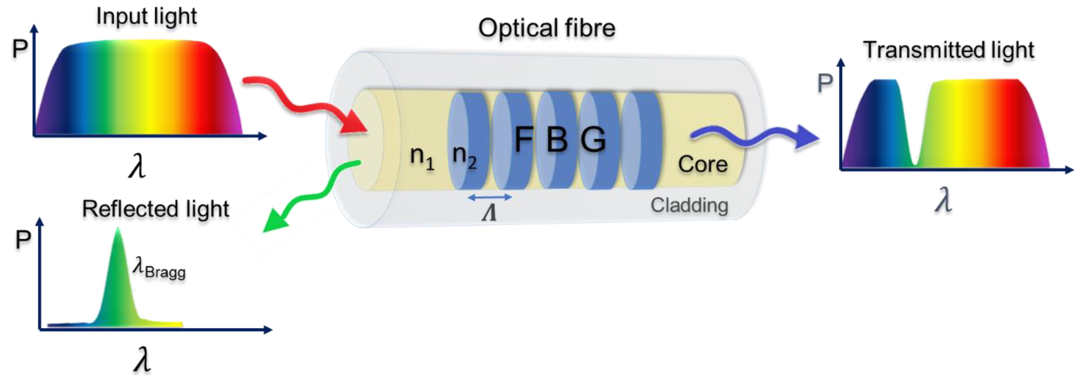
Figure 2.
(a) Sputtering mask with 3 optical fibers with an FBG in the center of the fiber where the plastic cover has been removed (in the yellow boxes). Nickel sputtered optical fiber with a thickness of 100nm, (b) Optical fiber after nickel chemical deposition of 5µm thickness.
Figure 2.
(a) Sputtering mask with 3 optical fibers with an FBG in the center of the fiber where the plastic cover has been removed (in the yellow boxes). Nickel sputtered optical fiber with a thickness of 100nm, (b) Optical fiber after nickel chemical deposition of 5µm thickness.
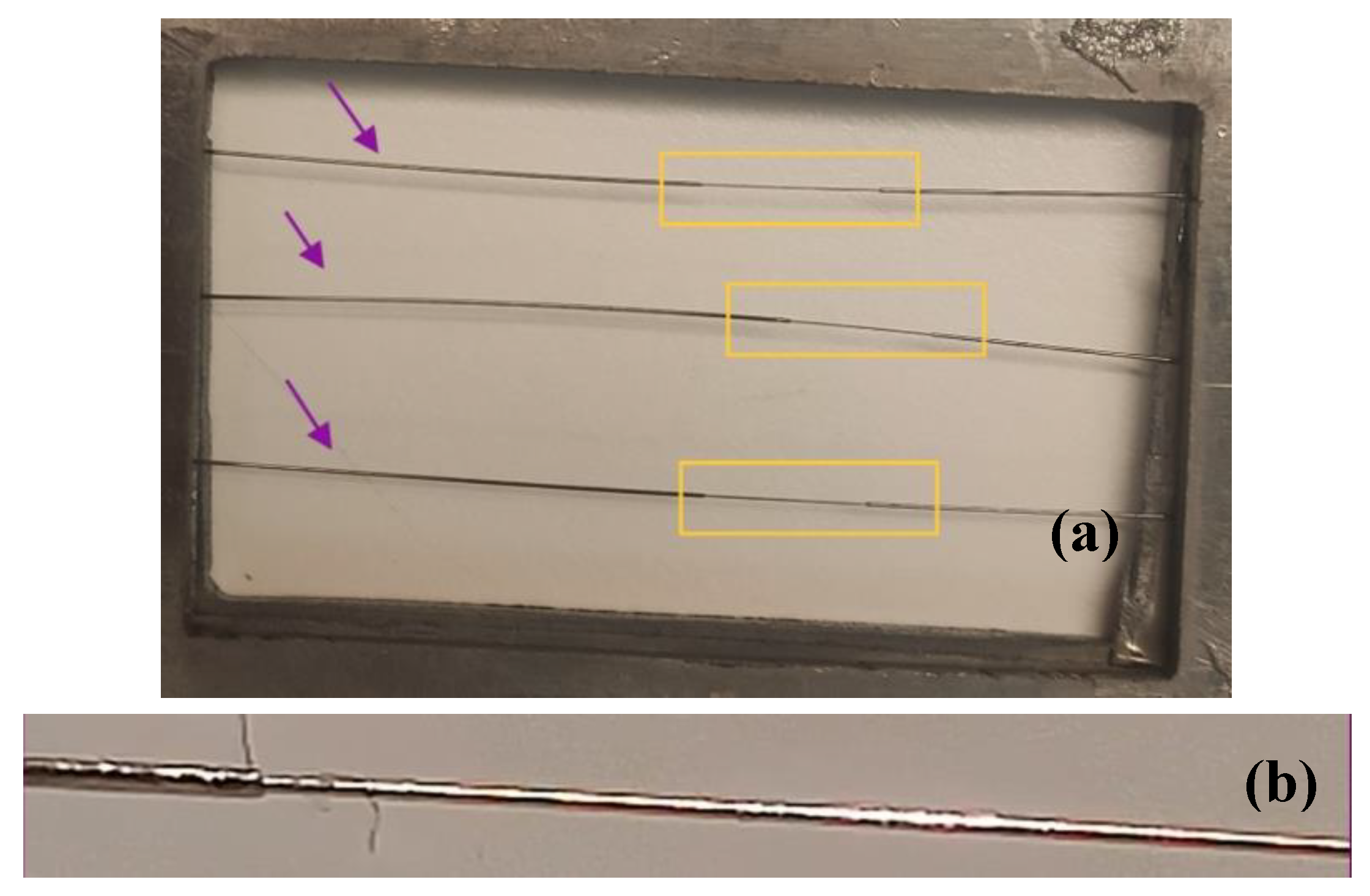
Figure 3.
SEM and EDX images of an optical fiber covered by Ni and Fe. These images reflects the deposited layers on the optical fiber. (a) SEM image of a sample where can be seen the optical fiber with a 135 μm diameter and the first layer of chemical deposition layer of Ni and the Fe layer by electrodeposition, (b) EDX image of the Ni layer (~5μm thickness) deposited on the optical fiber by chemical deposition, (c) EDX image of the Si due to the SiO2 of the optical fiber, (d) EDX of Fe layer (~30 μm thickness, attempt to electroplate GaxFe1-x, but only Fe was deposited as the density of current employed was over 40mA/cm2, with 7mA on an optical fiber of 3.5cm length), (e) EDX image of the O due to the SiO2 in the optical fiber.
Figure 4.
: saturation magnetostriction for bulk Fe1-x Gax. Reproduced graph from “Magnetization, Magnetic Magnetization, Anisotropy and Magnetostriction of Galfenol Alloys”, A. E. Clark, M. Wun-Fogle, and J. B. Restorff. Navsea, warfare centers, 2005 University of Maryland. Furnace cooled and multi-phase can have a magnetostriction constant below 150.
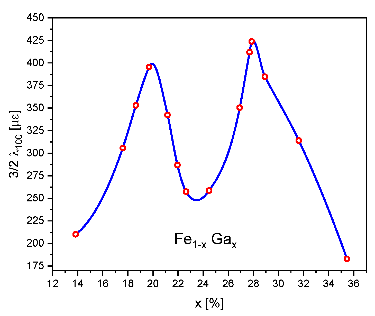
Figure 5.
Electrodeposition system with three electrodes.
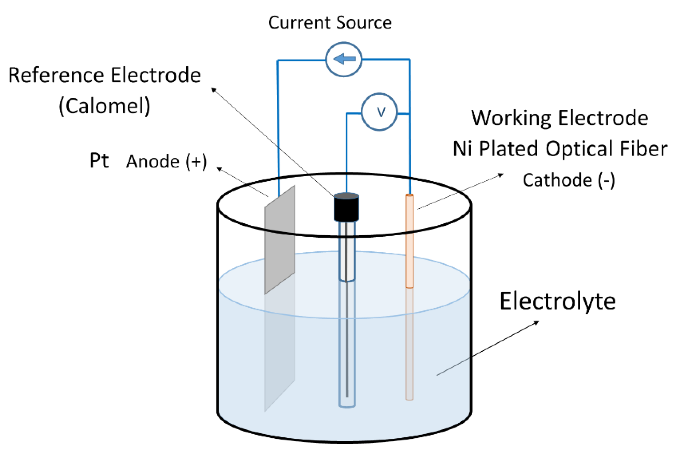
Figure 6.
Electrodeposition system with a current source.
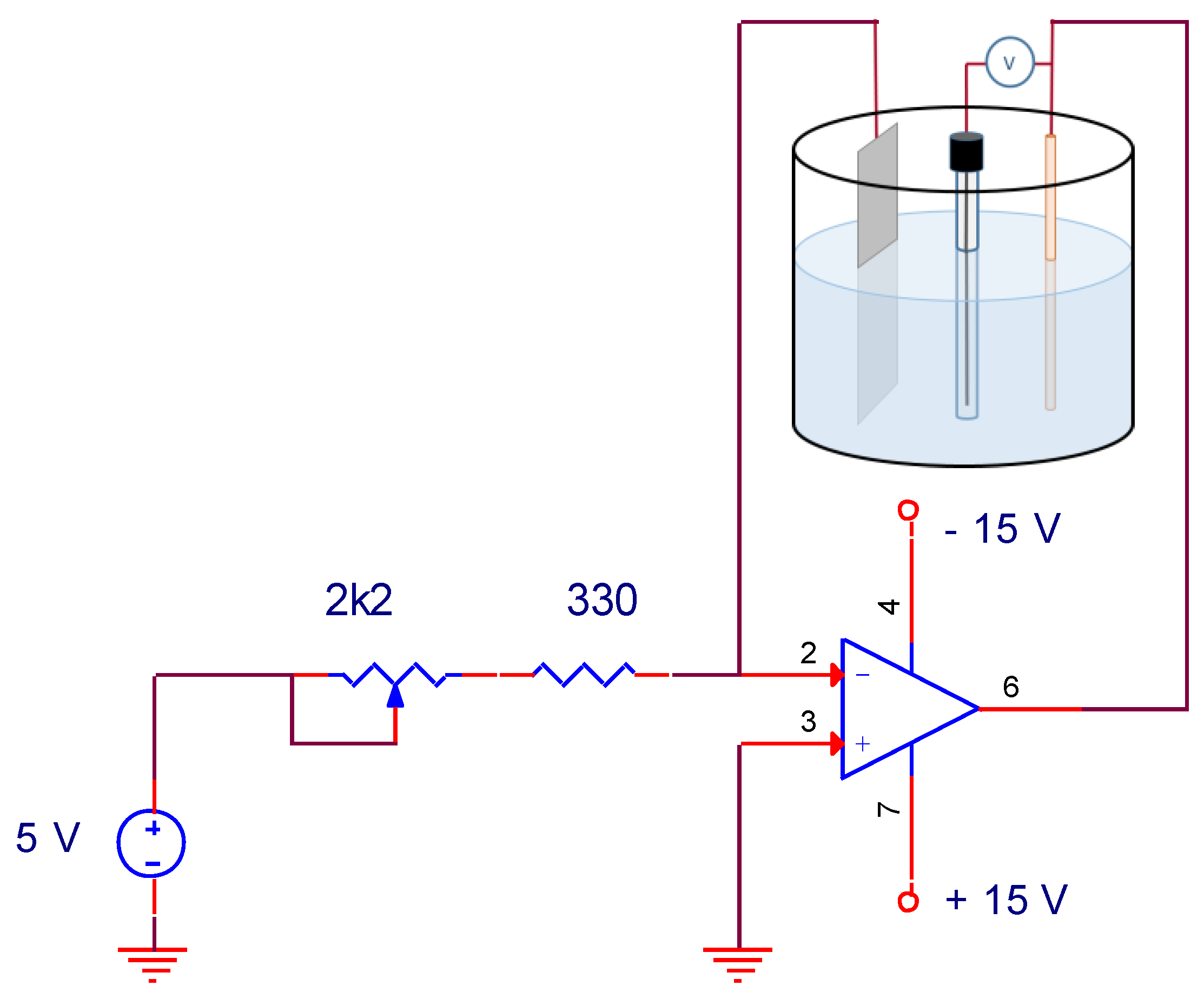
Figure 7.
(a) Schematic of the coil system for measuring hysteresis loops. (b) Image of the driven coil for the magnetic field generation with a driven magnetic field sensitivity of 7,7 kA/m.A. (c) Image of the pick-up coils for the measurement of the magnetization of the sample. Exciter coil with characteristics: N1=140, N2=10, l=14cm.
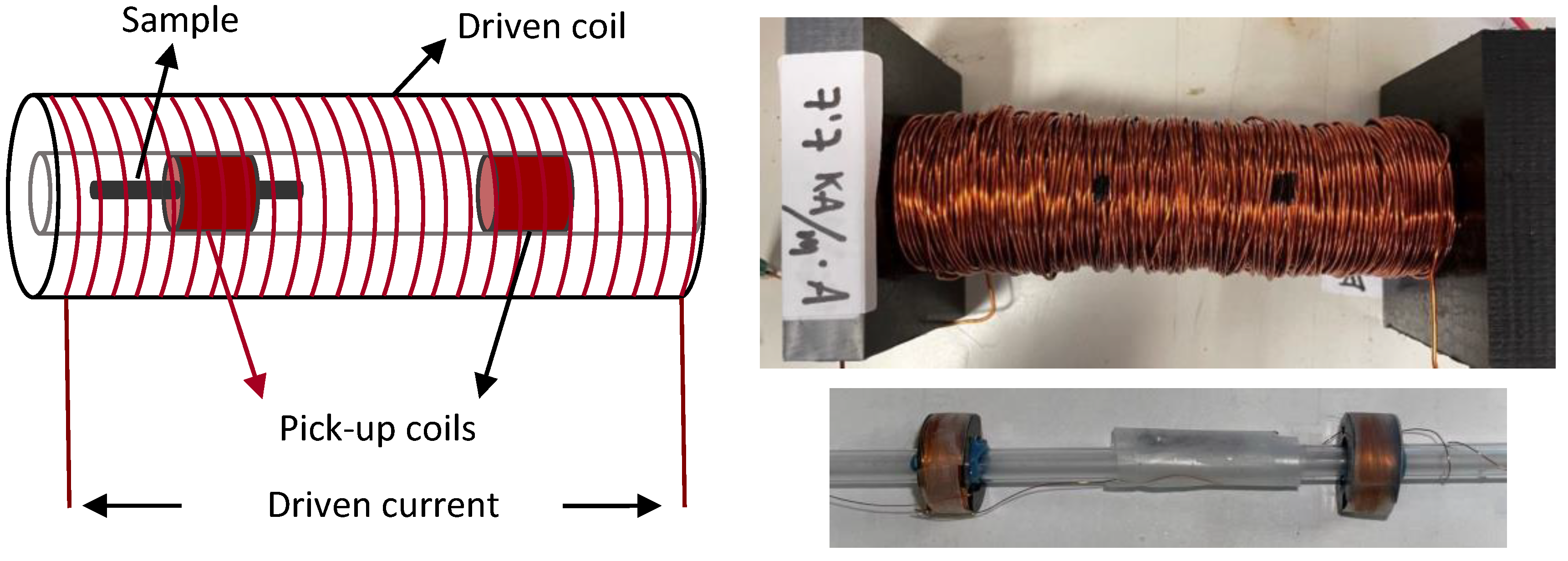
Figure 8.
(a) General scheme of the structure of the complete system used to obtain the hysteresis cycles of a magnetic sample. (b) Measuring system and assembled in the laboratory in order to obtain and capture the magnetic hysteresis cycles of the manufactured samples.
Figure 8.
(a) General scheme of the structure of the complete system used to obtain the hysteresis cycles of a magnetic sample. (b) Measuring system and assembled in the laboratory in order to obtain and capture the magnetic hysteresis cycles of the manufactured samples.
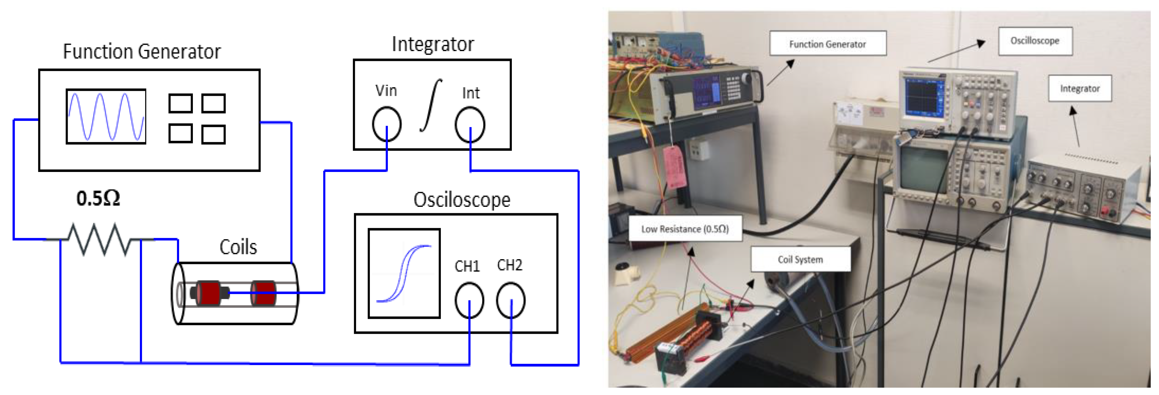
Figure 9.
EDX analysis of the sample 1, giving the percentage between Ga and Fe (see Table 4).
Figure 9.
EDX analysis of the sample 1, giving the percentage between Ga and Fe (see Table 4).
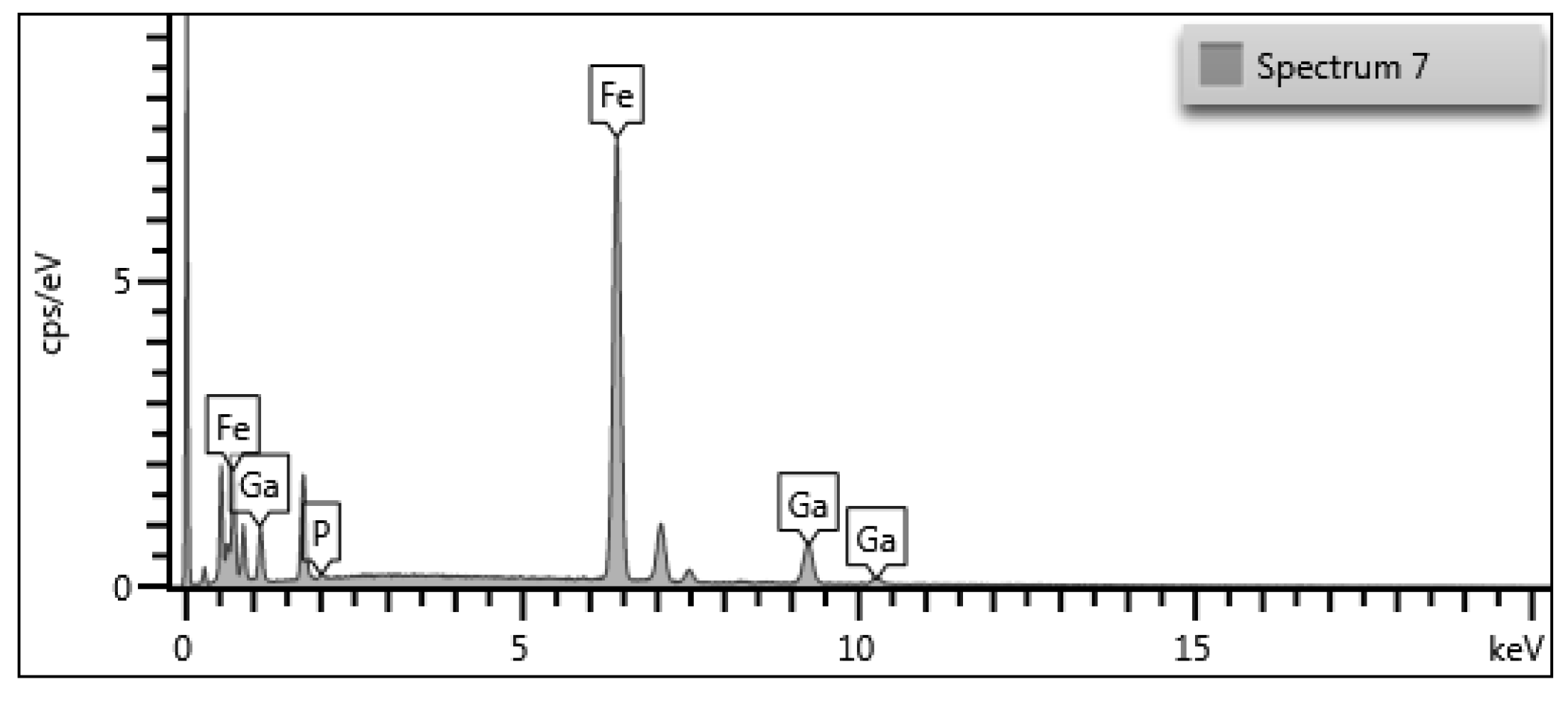
Figure 10.
(a) SEM image of an optical fiber covered by a 7μm thickness of FeGa; with 24% of Ga and 76% Fe, measured by EDX (Table 4), (b) Detail of the 7μm thickness of Galfenol where it can be seen a Ni layer of 1μm thickness deposited by chemical deposition between Galfenol and the optical fiber.

Figure 11.
Magnetostriction measurement of sample 1, measured applying a triangular current of 6A amplitude (92kA/m). Saturation is gotten for a current of 1A, which corresponds to a magnetic field of 7,7kA/m. The magnetostriction is only around 4pm in Δλ which correspond to a magnetostriction λS = 4.5. It has to be to consider that a Galfenol thickness of 7μm is stressing an optical fiber of 125μm in diameter.
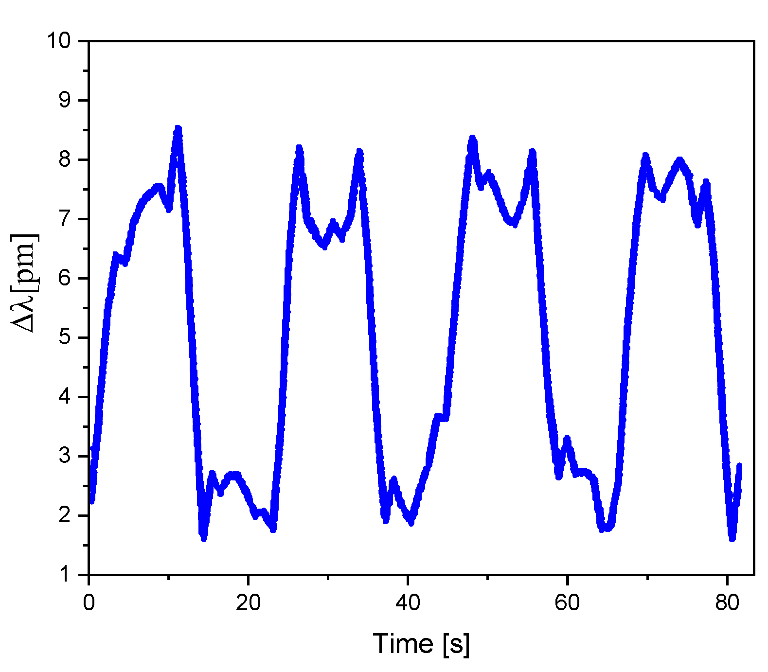
Figure 12.
(a) SEM of sample 2. It can be seen the optical fiber in the center and a layer of 126μm thickness of Galfenol, (b) Detail of the Ni layer of 7 µm thickness grown by chemical deposition.
Figure 12.
(a) SEM of sample 2. It can be seen the optical fiber in the center and a layer of 126μm thickness of Galfenol, (b) Detail of the Ni layer of 7 µm thickness grown by chemical deposition.
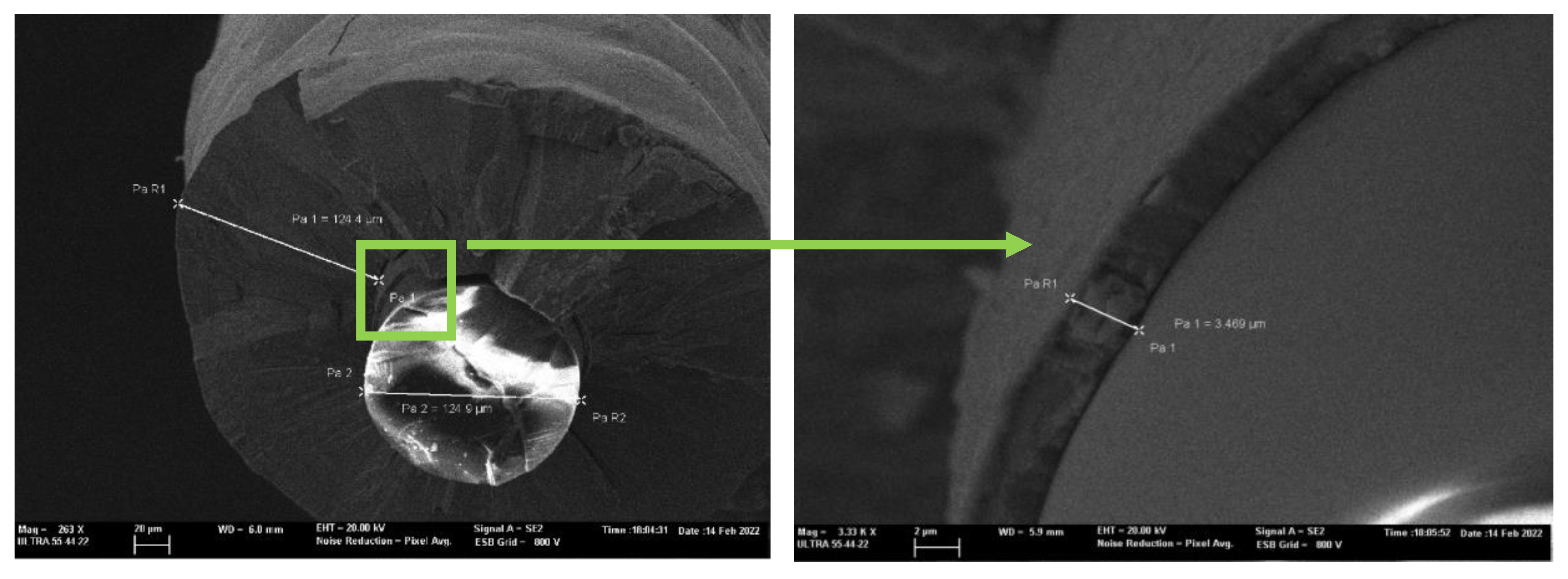
Figure 13.
Sample 2, (a) current density versus radius, (b) Gallium percentage versus current density. With manufacture parameters of 2.5 mA constant current and pH of 4.2.
Figure 13.
Sample 2, (a) current density versus radius, (b) Gallium percentage versus current density. With manufacture parameters of 2.5 mA constant current and pH of 4.2.
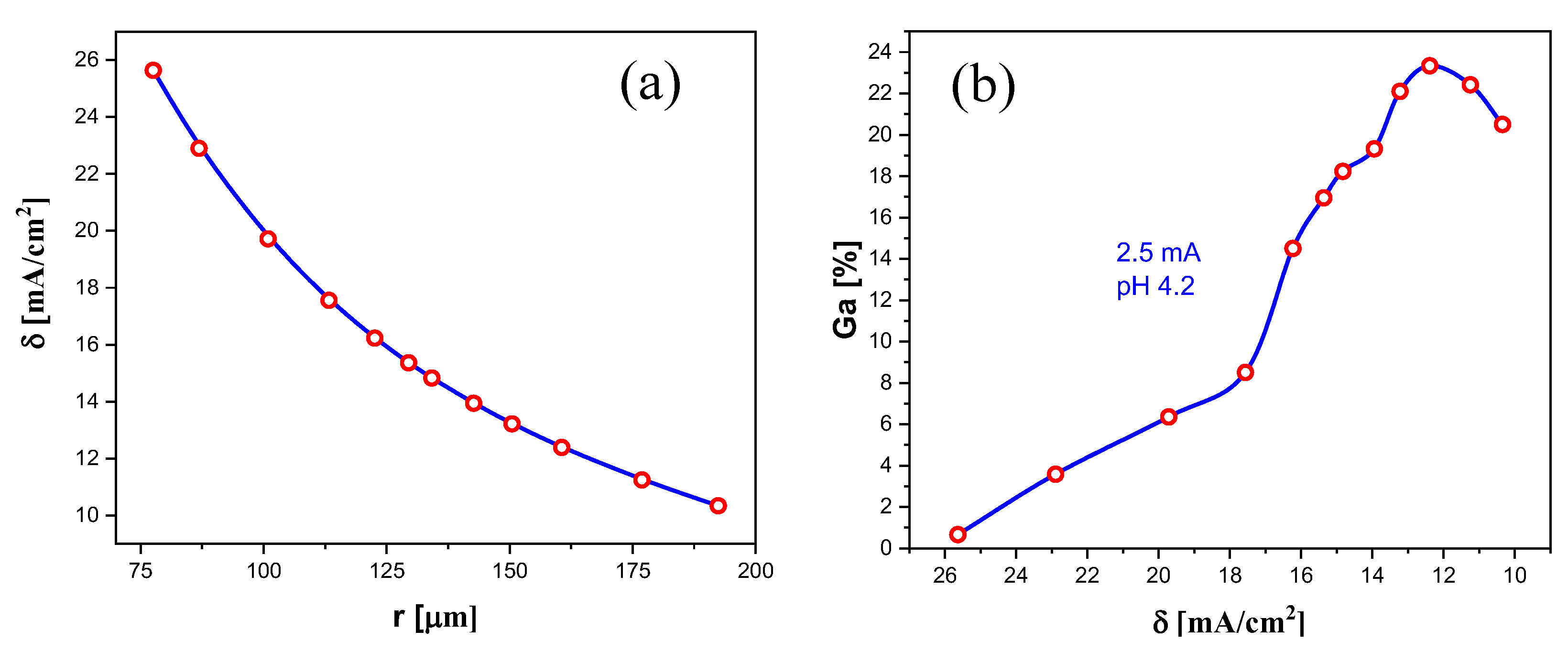
Figure 14.
(a),(b) SEM image of sample 2. Optical fiber diameter 135µm and Galfenol width of 128µm. Points with a number are where the EDX analysis have been done, (c) EDX image of Fe and, (d,f) EDX image of Si of the SiO2 from the optical fiber, (e) EDX image of Ga, (f) EDX image of O from the SiO2 of the optical fiber.
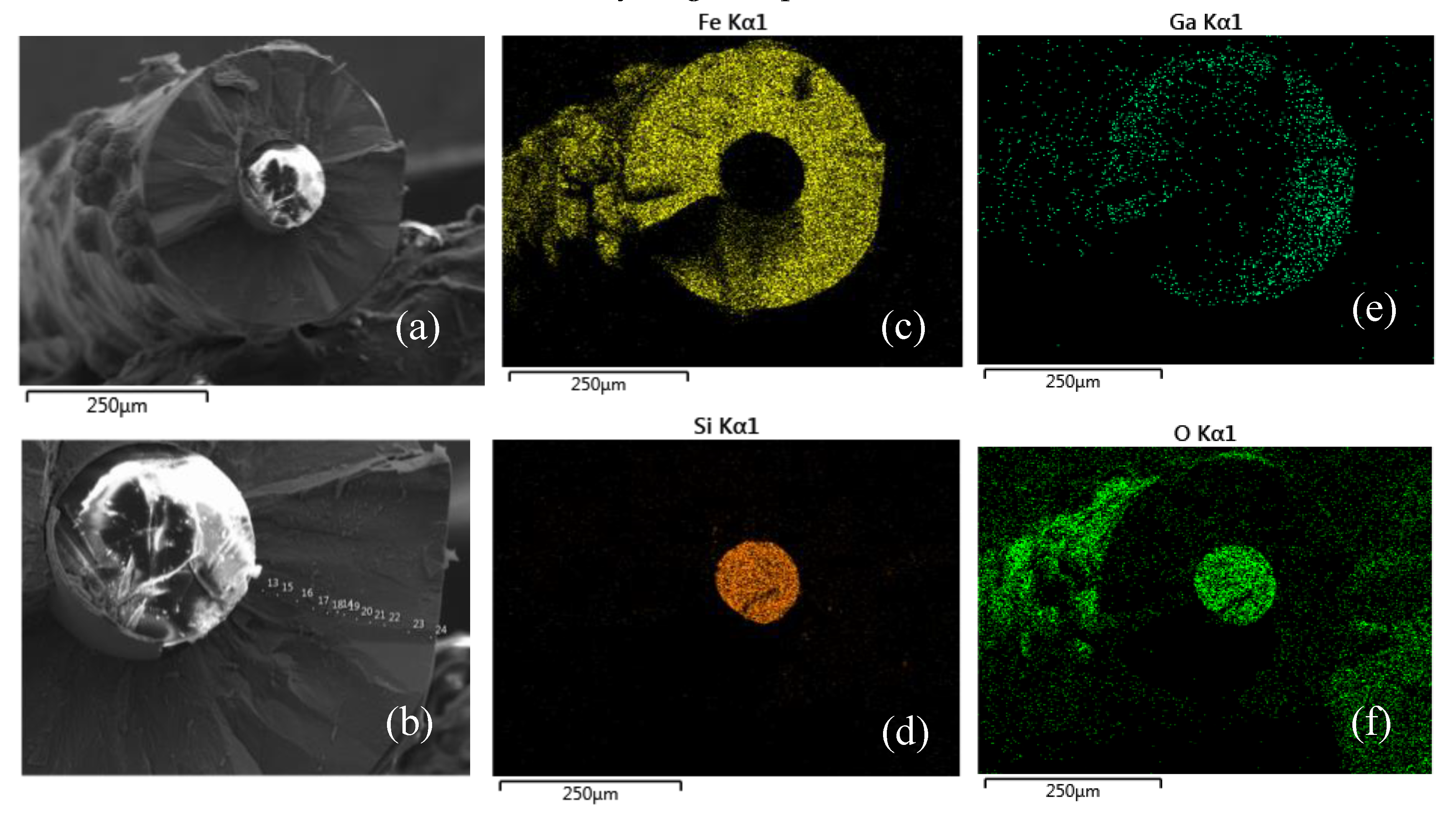
Figure 15.
(a) image captured in the oscilloscope with the sinusoidal signal proportional to the current in the driven coil (orange signal) and the voltage induced in the pick-up coil (blue signal), (b) current in the driven coil (orange) and the integration of the signal from the pick-up coils (blue).
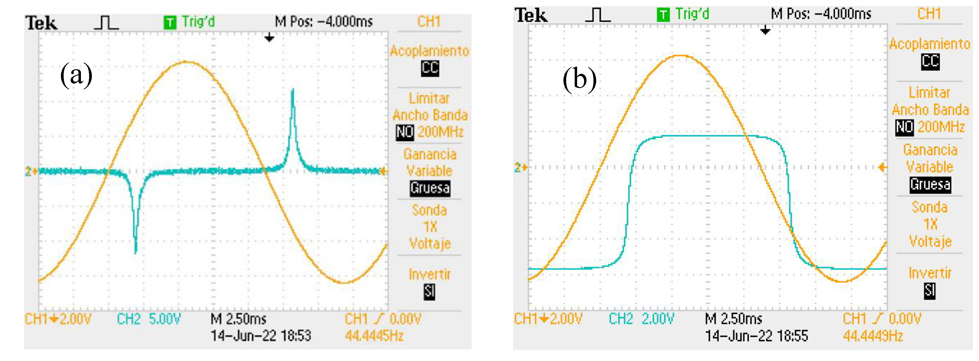
Figure 16.
hysteresis loops of sample 10 at (a) 14 Hz, (b) 28 Hz, (c) 43 Hz.
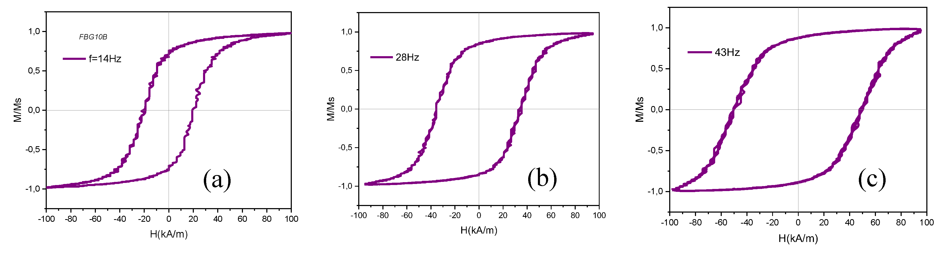
Figure 17.
(a) optical image of sample 2, (b) magnetostriction measurement applying a square signal of 70kA/m. The saturation magnetostriction is 8pm.
Figure 17.
(a) optical image of sample 2, (b) magnetostriction measurement applying a square signal of 70kA/m. The saturation magnetostriction is 8pm.
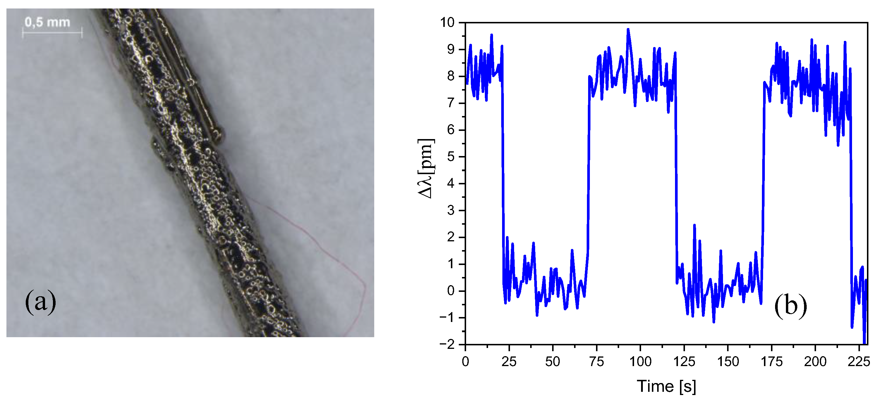
Figure 18.
Sample 3 grown in two zones, first stretch with 2.5mA and pH 3.9 and second stretch with 7.5mA and pH 4.4 (a) current density versus radius, (b) Ga percentage versus radius, (c) Ga percentage versus current density.
Figure 18.
Sample 3 grown in two zones, first stretch with 2.5mA and pH 3.9 and second stretch with 7.5mA and pH 4.4 (a) current density versus radius, (b) Ga percentage versus radius, (c) Ga percentage versus current density.
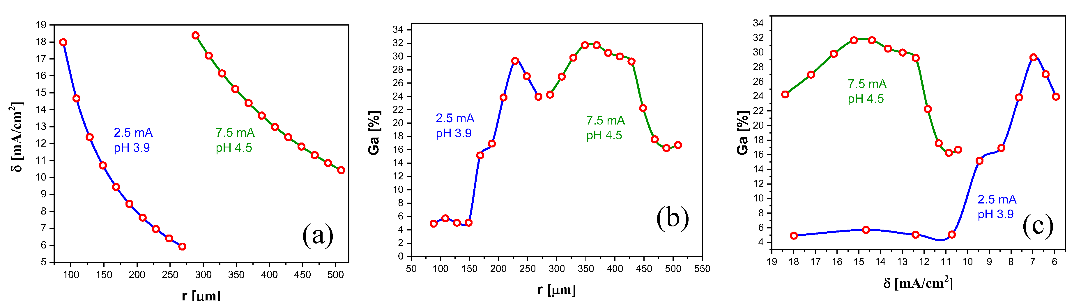
Figure 19.
(a) SEM image of sample 3. Optical fiber diameter 135µm and Galfenol width of 430µm, (b) EDX image of Fe and (c) EDX image of Ga (x marks on the image are the EDX measurement points to get the percentage of Ga).
Figure 19.
(a) SEM image of sample 3. Optical fiber diameter 135µm and Galfenol width of 430µm, (b) EDX image of Fe and (c) EDX image of Ga (x marks on the image are the EDX measurement points to get the percentage of Ga).
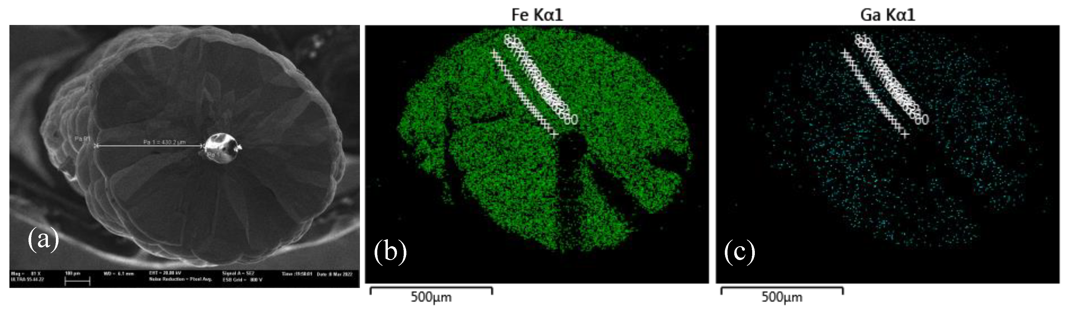
Figure 20.
Sample 4, grown in two zones, first stretch with 2.5mA and pH 5.9 and second stretch with 12.5mA and pH 5.9 (a) Current density versus radius, (b) Ga percentage versus current density.
Figure 20.
Sample 4, grown in two zones, first stretch with 2.5mA and pH 5.9 and second stretch with 12.5mA and pH 5.9 (a) Current density versus radius, (b) Ga percentage versus current density.
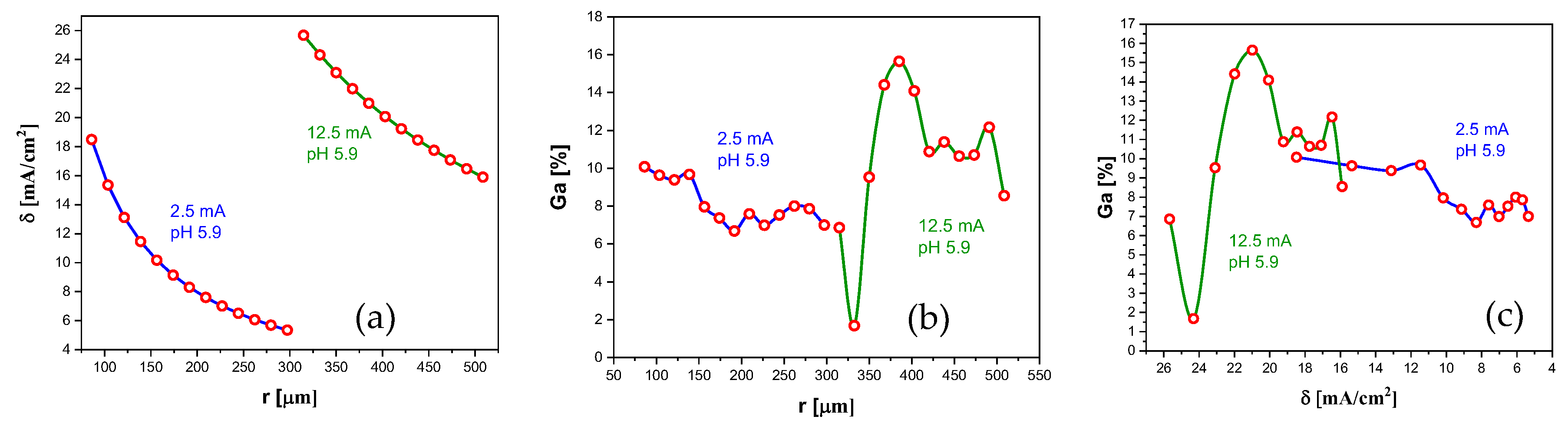
Figure 21.
(a) SEM image of sample 3. Optical fiber diameter 135µm and Galfenol width of 430µm, (b) EDX image of Fe and (c) EDX image of Ga (x marks on the image are the EDX measurement points).
Figure 21.
(a) SEM image of sample 3. Optical fiber diameter 135µm and Galfenol width of 430µm, (b) EDX image of Fe and (c) EDX image of Ga (x marks on the image are the EDX measurement points).
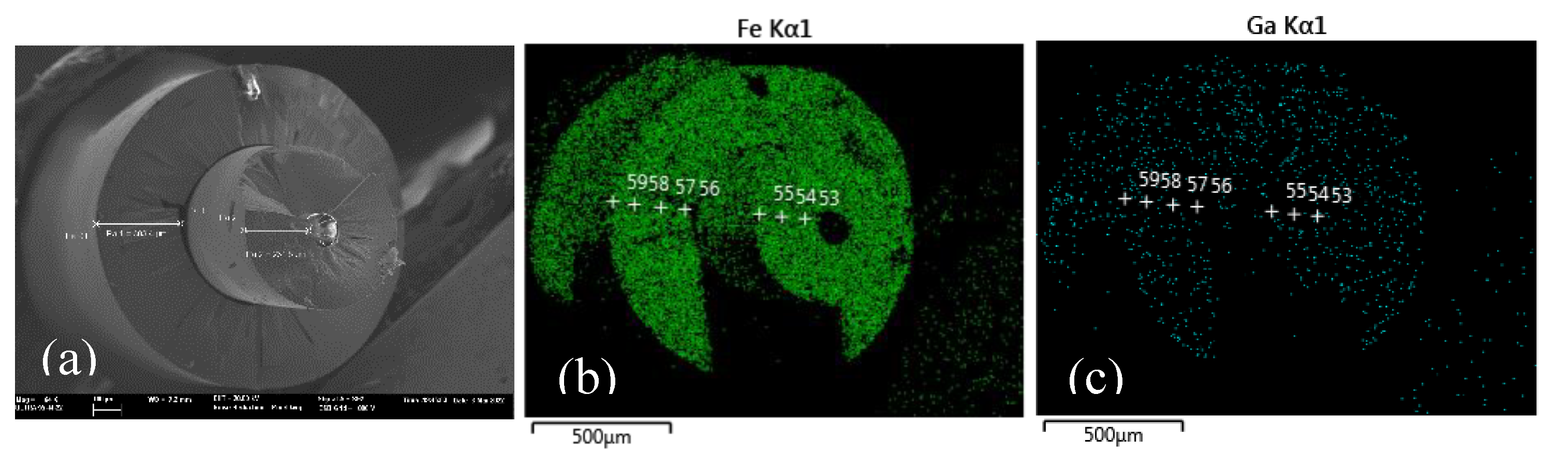
Figure 22.
Sample 4, grown in two zones, first stretch with 3mA and pH 4 and second stretch with 4.5mA and pH 4.5 (a) current density versus radius, (b) Ga percentage versus radius for the two currents and pH, (b) Ga percentage versus current density for both currents and pH.
Figure 22.
Sample 4, grown in two zones, first stretch with 3mA and pH 4 and second stretch with 4.5mA and pH 4.5 (a) current density versus radius, (b) Ga percentage versus radius for the two currents and pH, (b) Ga percentage versus current density for both currents and pH.
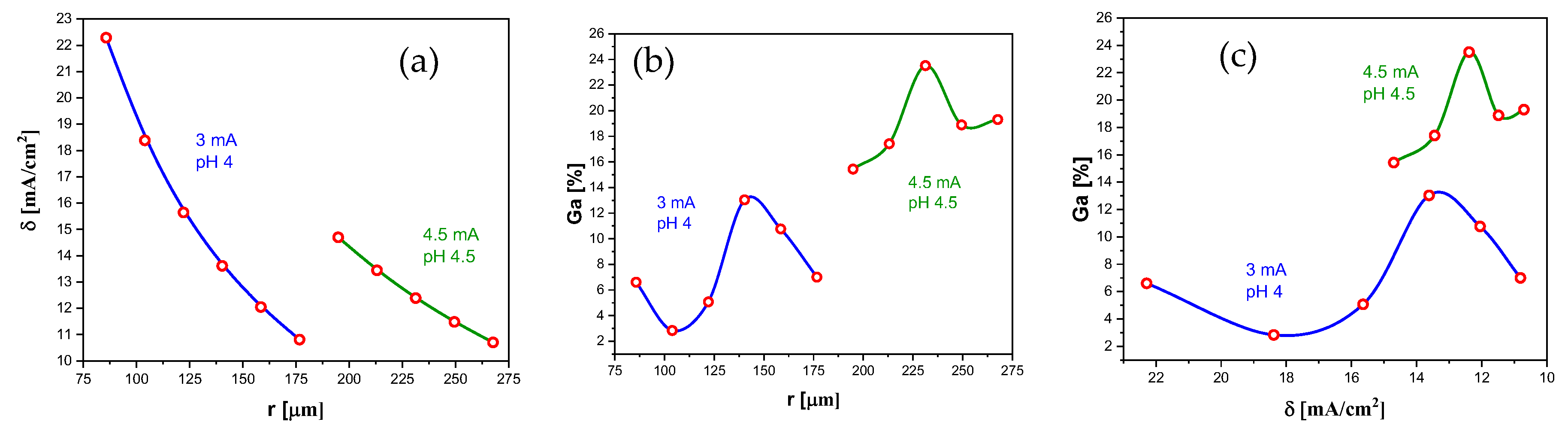
Figure 23.
(a) SEM image of sample 5. Optical fiber diameter 135µm and Galfenol width of 200µm, (b) zoom of the Galfenol layer where can be seen a quite homogeneous texture of the Galfenol.
Figure 23.
(a) SEM image of sample 5. Optical fiber diameter 135µm and Galfenol width of 200µm, (b) zoom of the Galfenol layer where can be seen a quite homogeneous texture of the Galfenol.
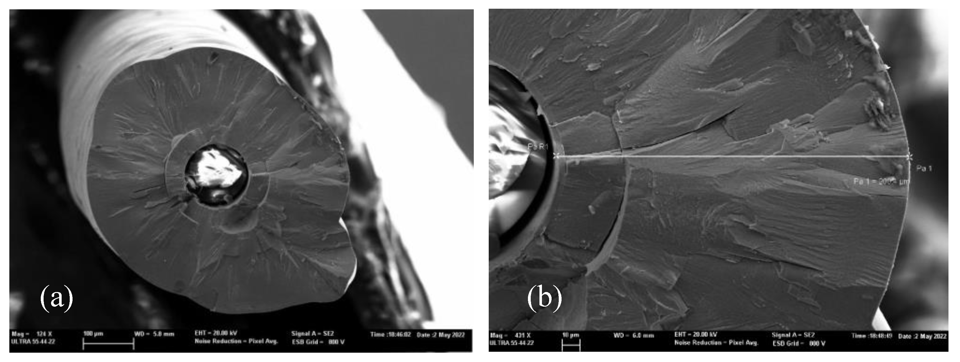
Figure 24.
(a) SEM image of sample 6. Optical fiber diameter 135µm and Galfenol width of 280µm, (b) Current density versus radius, (c) percentage of Ga versus radius, (d) percentage of Ga versus current density.
Figure 24.
(a) SEM image of sample 6. Optical fiber diameter 135µm and Galfenol width of 280µm, (b) Current density versus radius, (c) percentage of Ga versus radius, (d) percentage of Ga versus current density.
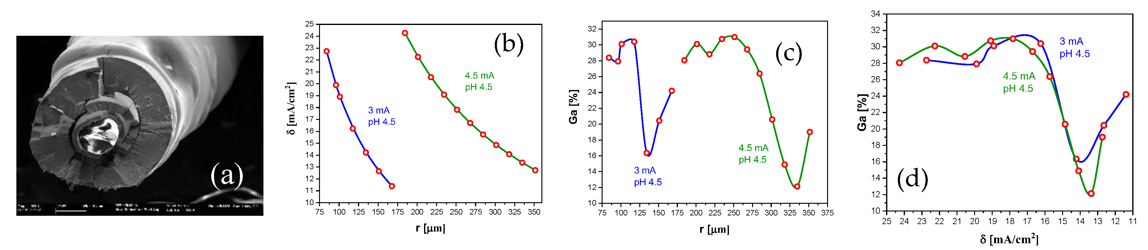
Figure 25.
Sample 7, grown in two zones, first stretch with 3mA and pH 5 and second stretch with 4.5mA and pH 5, (a) current density versus radius, (b) percentage of Ga versus radius, (c) Ga percentage versus current density.
Figure 25.
Sample 7, grown in two zones, first stretch with 3mA and pH 5 and second stretch with 4.5mA and pH 5, (a) current density versus radius, (b) percentage of Ga versus radius, (c) Ga percentage versus current density.
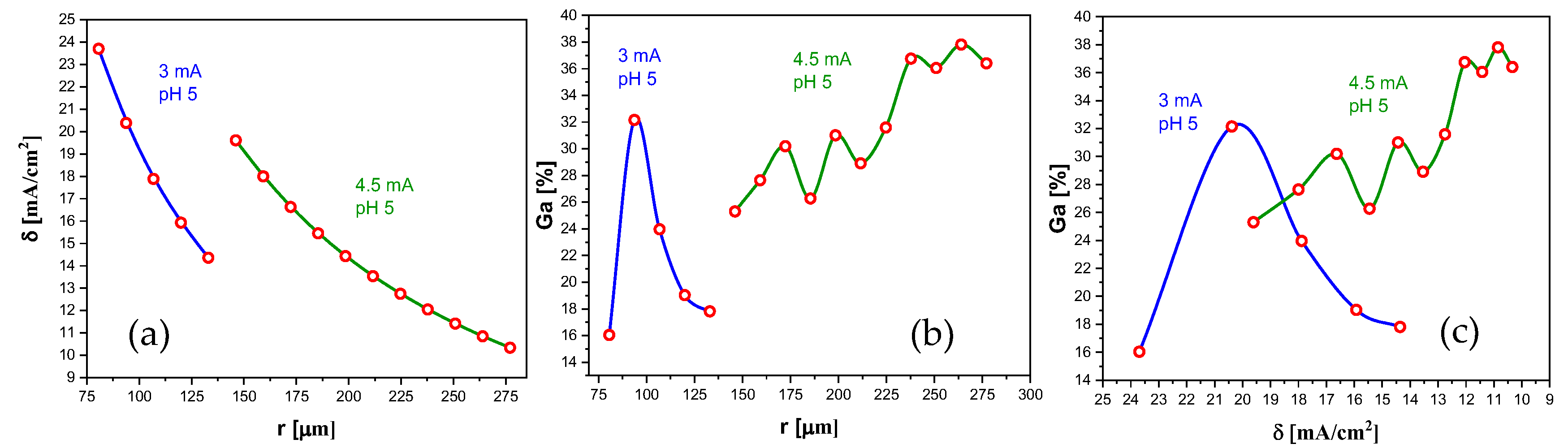
Figure 26.
(a) SEM image of sample 7 with 207μm of thickness of Galfenol, (b) Rugosity and uniformity of electrodeposition of Galfenol with different pH, (b) sample 6 grown with pH 4.5, (c) sample 7 grown with pH 5.
Figure 26.
(a) SEM image of sample 7 with 207μm of thickness of Galfenol, (b) Rugosity and uniformity of electrodeposition of Galfenol with different pH, (b) sample 6 grown with pH 4.5, (c) sample 7 grown with pH 5.
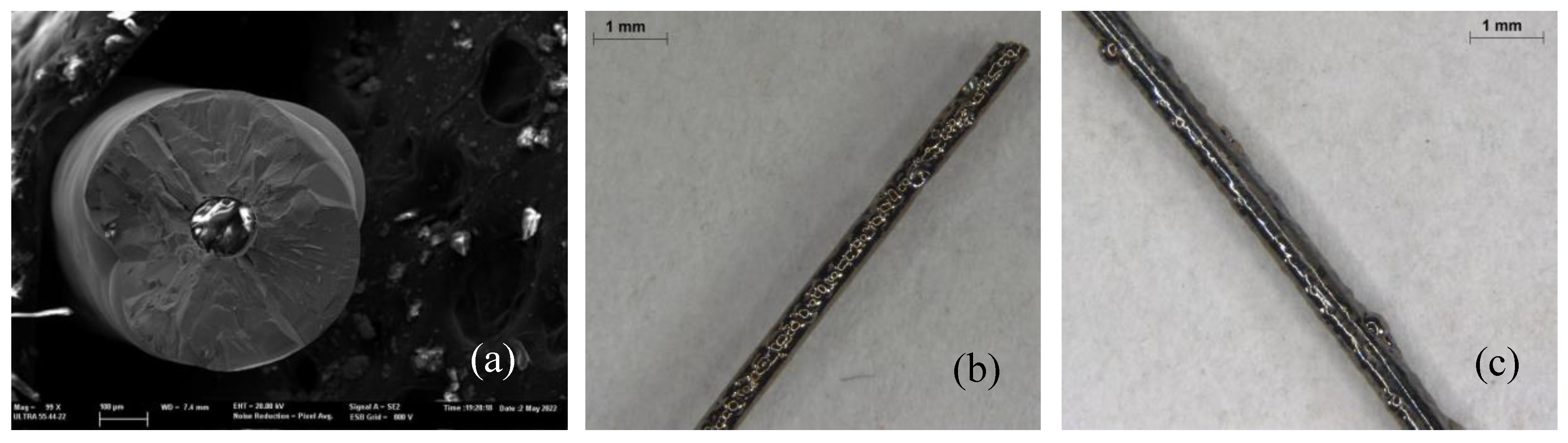
Figure 27.
Sample 8, grown with 5mA and pH 5, (a) current density versus radius, (b) percentage of Ga versus radius, (c) Ga percentage versus current density.
Figure 27.
Sample 8, grown with 5mA and pH 5, (a) current density versus radius, (b) percentage of Ga versus radius, (c) Ga percentage versus current density.
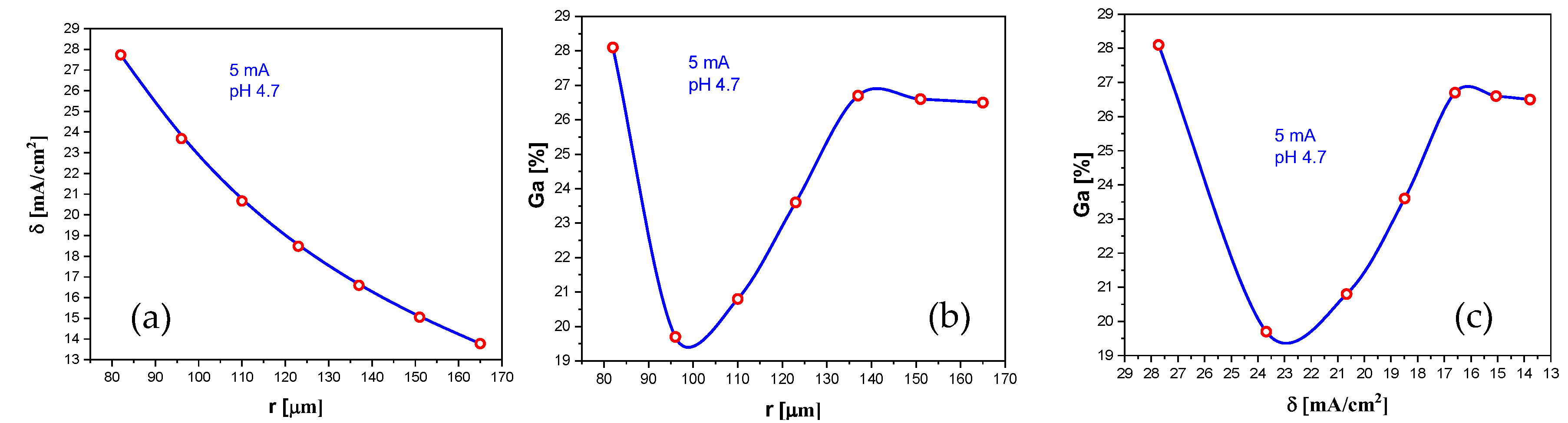
Figure 28.
(a) SEM image of an optical fiber covered by a 97μm thickness of Galfenol, (b) plot of magnetostriction applying a square unipolar magnetic field to saturation, getting a magnetostriction of 9pm measured with the wavelength shift which corresponds to a 9.9 με of magnetostriction.
Figure 28.
(a) SEM image of an optical fiber covered by a 97μm thickness of Galfenol, (b) plot of magnetostriction applying a square unipolar magnetic field to saturation, getting a magnetostriction of 9pm measured with the wavelength shift which corresponds to a 9.9 με of magnetostriction.
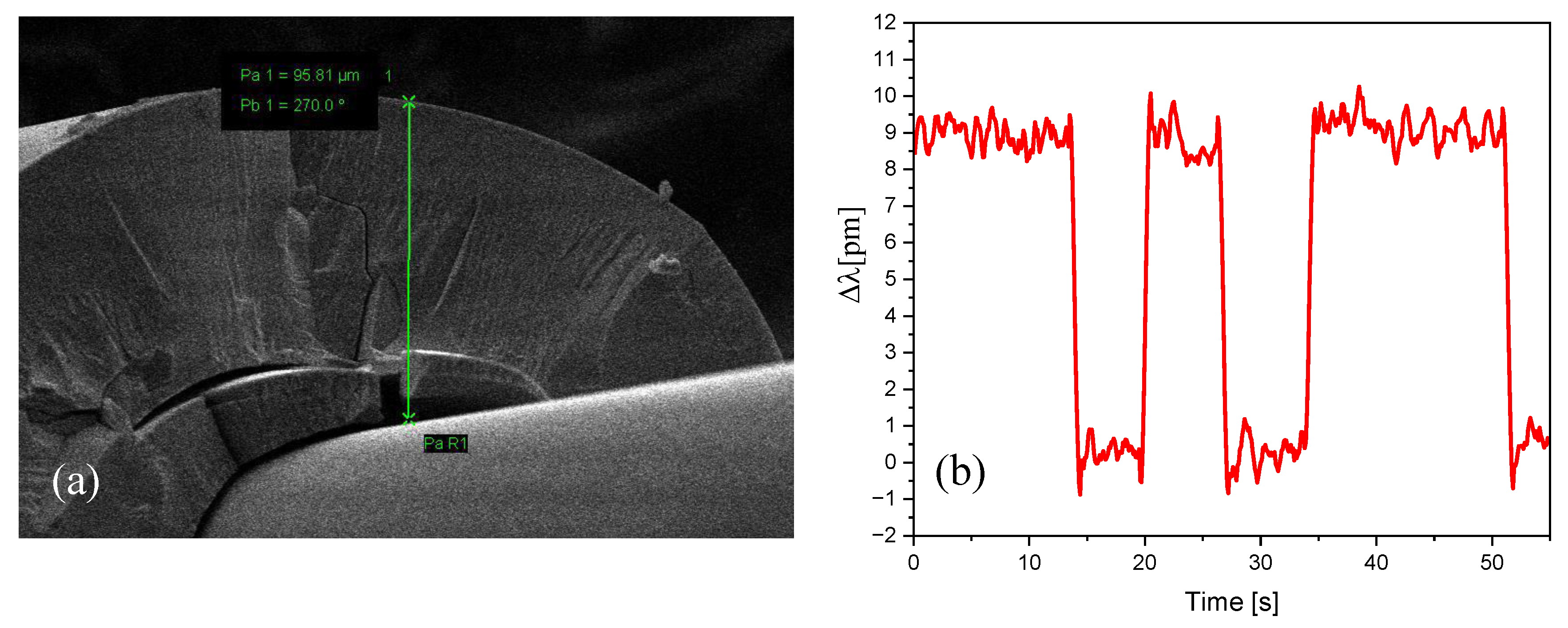
Figure 29.
Sample 9, grown with 6mA and pH 4.5, (a) current density versus radius, (b) percentage of Ga versus radius, (c) Ga percentage versus current density.
Figure 29.
Sample 9, grown with 6mA and pH 4.5, (a) current density versus radius, (b) percentage of Ga versus radius, (c) Ga percentage versus current density.
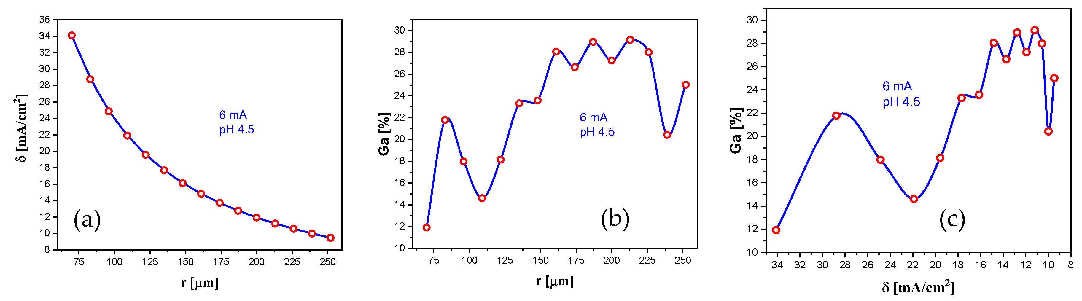
Figure 30.
Hysteresis loop of sample 9, (a) as cast, (b) after current and temperature annealing with 400mA during 30 minutes and temperature of 350 ºC.
Figure 30.
Hysteresis loop of sample 9, (a) as cast, (b) after current and temperature annealing with 400mA during 30 minutes and temperature of 350 ºC.
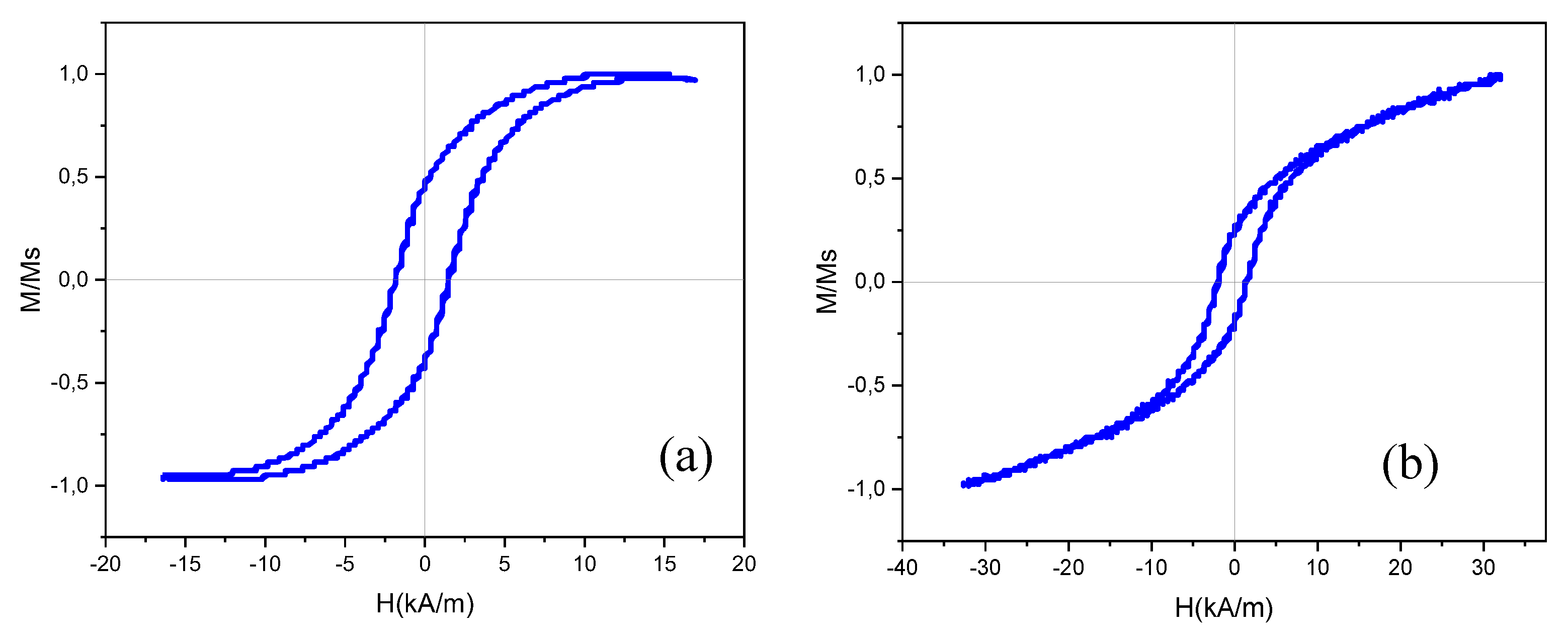

Table 1.
Solution of electroless nickel plating.
| Component | 250 mL |
|---|---|
| Nickel Chloride (NiCl2) | 14 g |
| Sodium Citrate (Na3 C6H5O7) | 25 g |
| Sodium Hypophosphite (NaP O2H2) | 22.5 g |
Table 2.
Solution for Galfenol Electrodeposition.
| Component | Concentration (M) | 500 mL |
|---|---|---|
| Gallium Sulphate (Ga2(SO4)3) | 0.06 | 12.83 g |
| Iron Sulphate (FeSO4) | 0.03 | 4.17 g |
| Boric Acid (H3BO3) | 0.50 | 15.46 g |
| Sodium Citrate (Na3C6H5O7) | 0.15 | 19.74 g |
| Ascorbic Acid (C6H8O6) | 0.04 | 3.52 g |
Table 3.
Manufacture parameters of sample 1.
| Sample 1 | Optical Fiber (OF) | OF + Sputtering (S) + Chemical Deposition (CHD) | OF + S + CHD + Electrodeposition (ELD) |
|---|---|---|---|
| Diameter | 135 µm | 137 µm | 151 µm |
| Length | 3.5 cm | 3.5 cm | 3.5 cm |
| Surface | - | 0.15 cm² | 0.17 cm² |
| Current | - | 3 mA | 3 mA |
| Current Density | - | 19.9 mA/cm² | 18.1 mA/cm² |
| pH | - | - | 2.5 |
| Time | - | - | 12 h |
Table 4.
EDX of sample 1 with the percentage of Ga and Fe.
| Element | Line Type | Apparent Concentration |
k Ratio | Wt% | Wt% Sigma |
|---|---|---|---|---|---|
| Fe | K series | 47,4 | 0,47402 | 75,87 | 0,32 |
| Ga | K series | 14,03 | 0,13151 | 24,13 | 0,32 |
| Total: | 100 |
Table 5.
Manufacture parameters of sample 2.
| Sample 2 | OF | OF + S + CHD | OF + S + CHD + ELD |
|---|---|---|---|
| Diameter | 135 µm | 143 µm | 395 µm |
| Length | 3.2 cm | 3.2 cm | 3.2 cm |
| Surface | - | 0.144 cm² | 0.397 cm² |
| Current | - | 4 mA | 4 mA |
| Current Density | - | 27.8 mA/cm² | 10.1 mA/cm² |
| pH | - | - | 4.2 |
| Time | - | - | 92 h |
Table 6.
Manufacture parameters of sample 3.
| Sample 3 | OF | OF + S + CHD | OF + S + CHD + ELD | OF + S + CHD + ELD |
|---|---|---|---|---|
| Diameter | 135 µm | 147 µm | 540 µm | 1000 µm |
| Length | 2.5 cm | 2.5 cm | 2 cm | 2 cm |
| Surface | - | 0.115 cm² | 0.34 cm² | 0.628 cm² |
| Current | - | 2.5 mA | 7.5 mA | 7.5 mA |
| Current Density | - | 21.6 mA/cm² | 22.1 mA/cm² | 11.9 mA/cm² |
| pH | - | 3.9 | 3.9 | 4.4 |
| Time | - | - | 48 h | 96 h |
Table 7.
Manufacture parameters of sample 4.
| Sample 4 | OF | OF + S + CHD | OF + S + CHD + ELD | OF + S + CHD + ELD |
|---|---|---|---|---|
| Diameter | 135 µm | 150 µm | 630 µm | 1017 µm |
| Length | 2.5 cm | 2.5 cm | 2.5 cm | 2.5 cm |
| Surface | - | 0.118 cm² | 0.49 cm² | 0.80 cm² |
| Current | - | 2.5 mA | 12.5 mA | 12.5 mA |
| Current Density | - | 23.4 mA/cm² | 25.7 mA/cm² | 15.9 mA/cm² |
| pH | - | 5.9 | 5.9 | 5.9 |
| Time | - | - | 48 h | 96 h |
Table 8.
Manufacture parameters of sample 5.
| Sample 5 | OF | OF + S + CHD | OF + S + CHD + ELD | OF + S + CHD + ELD |
|---|---|---|---|---|
| Diameter | 135 µm | 145 µm | 384 µm | 536 µm |
| Length | 2.5 cm | 2.5 cm | 2.5 cm | 2.5 cm |
| Surface | - | 0.118 cm² | 0.30 cm² | 0.42 cm² |
| Current | - | 3 mA | 4.5 mA | 4.5 mA |
| Current Density | - | 25.4 mA/cm² | 15 mA/cm² | 10.7 mA/cm² |
| pH | - | - | 4 | 4.5 |
| Time | - | - | 48 h | 96 h |
Table 9.
Manufacture parameters of sample 6.
| Sample 6 | OF | OF + S + CHD | OF + S + CHD + ELD | OF + S + CHD + ELD |
|---|---|---|---|---|
| Diameter | 135 µm | 143 µm | 340 µm | 703 µm |
| Length | 2.5 cm | 2.5 cm | 1.6 cm | 1.6 cm |
| Surface | - | 0.107 cm² | 0.192 cm² | 0.397 cm² |
| Current | - | 3 mA | 4.5 mA | 4.5 mA |
| Current Density | - | 27.8 mA/cm² | 23.4 mA/cm² | 11.3 mA/cm² |
| pH | - | - | 4.5 | 4.5 |
| Time | - | - | 48 h | 96 h |
Table 10.
Manufacture parameters of sample 7.
| Sample 7 | OF | OF + S + CHD | OF + S + CHD + ELD | OF + S + CHD + ELD |
|---|---|---|---|---|
| Diameter | 135 µm | 139 µm | 278 µm | 554 µm |
| Length | 2.5 cm | 2.5 cm | 2.5 cm | 2.5 cm |
| Surface | - | 0.109 cm² | 0.218 cm² | 0.435 cm² |
| Current | - | 3 mA | 4.5 mA | 4.5 mA |
| Current Density | - | 27.5 mA/cm² | 20.6 mA/cm² | 10.3 mA/cm² |
| pH | - | - | 5 | 5 |
| Time | - | - | 48 h | 96 h |
Table 11.
Manufacture parameters of sample 8.
| Sample 8 | OF | OF + S + CHD | OF + S + CHD + ELD |
|---|---|---|---|
| Diameter | 135 µm | 145 µm | 330 µm |
| Length | 3.5 cm | 3.5 cm | 3.5 cm |
| Surface | - | 0.15 cm² | 0.17 cm² |
| Current | - | 5 mA | 5 mA |
| Current Density | - | 30.3 mA/cm² | 13.8 mA/cm² |
| pH | - | - | 5 |
| Time | - | - | 48 h |
Table 12.
Manufacture parameters of sample 9.
| Sample 9 | OF | OF + S + CHD | OF + S + CHD + ELD |
|---|---|---|---|
| Diameter | 135 µm | 142 µm | 504 µm |
| Length | 4 cm | 4 cm | 4 cm |
| Surface | - | 0.367 cm² | 0.633 cm² |
| Current | - | 6 mA | 6 mA |
| Current Density | - | 33.6 mA/cm² | 9.5 mA/cm² |
| pH | - | - | 4.5 |
| Time | - | - | 72 h |
Disclaimer/Publisher’s Note: The statements, opinions and data contained in all publications are solely those of the individual author(s) and contributor(s) and not of MDPI and/or the editor(s). MDPI and/or the editor(s) disclaim responsibility for any injury to people or property resulting from any ideas, methods, instructions or products referred to in the content. |
© 2024 by the authors. Licensee MDPI, Basel, Switzerland. This article is an open access article distributed under the terms and conditions of the Creative Commons Attribution (CC BY) license (http://creativecommons.org/licenses/by/4.0/).
Copyright: This open access article is published under a Creative Commons CC BY 4.0 license, which permit the free download, distribution, and reuse, provided that the author and preprint are cited in any reuse.


