Submitted:
27 March 2024
Posted:
28 March 2024
You are already at the latest version
Abstract
In this study, Silicon Carbide (SiC) nano-particle based serigraphic printing inks were
formulated to fabricate highly sensitive and wide temperature range SiC printed thermistors. Initially,
commercial silver ink was screen printed to fabricate inter-digitated electrodes (IDE’s) onto flexible
Kapton® substrate via screen printing. Thermistor inks with different weight ratios of SiC nano-
particles dispersed in polyimide resin matrix were fabricated. The SiC-polyimide temperature sensing
inks were screen printed atop the IDE structures to form fully printed thermistors and encapsulated
with a adhesive backed polyimide film for humidity inhibition. The high temperature tolerance
of the Kapton® allowed the the sensors to be tested over a wide temperature range form 25◦C to
170◦C. The printed SiC thermistors exhibit excellent repeatability and stability over 15 hours of
continuous operation. Optimal device performance was achieved with 30 wt.% SiC-polyimide ink.
We report highly sensitive devices with a temperature coefficient of Resistance (TCR) of -0.556 %/◦C,
a thermal coefficient of 502 K (β-index) and an activation energy of 0.08 eV which are comparable with
printed thermistors previous reported. Further, the thermistor demonstrates an accuracy of ±1.35◦C
which is well within the range offered by commercially available high sensitivity thermistors. SiC
thermistors exhibit a small 6.5% drift due to changes in relative humidity between 10-90 %RH and a
4.2 % drift in baseline resistance after 100 cycles of aggressive bend testing at a 40°angle. The use of
commercially available low cost materials, simplicity of design and fabrication techniques coupled
with the chemical inertness of the Kapton® substrate and SiC nanoparticles paves the way to use
all-printed SiC thermistors towards a wide range of applications where temperature monitoring is
vital for optimal system performance.
Keywords:
Temperature Sensing
; Negative Temperature Coefficient (NTC)
; Printed Electronics
; Printed Temperature Sensors
; Thermistors
; Silicon Carbide
; Wide Band-gap Semiconductor
; Screen Printing
; Silver ink
1. Introduction
Temperature sensing is crucial in key industries such as automotive [1], health [2,3], aerospace [4], agriculture [5] and consumer electronics [6]. Measuring temperature is a key variable in controlling and monitoring the intended function of a system [7] to and to optimize process yields [8]. The three predominant types of printed temperature sensors are: 1. resistance temperature detectors (RTD’s) [9], 2. thermocouples [10] and 3. thermistors [11]. Choosing the correct type of temperature sensor is dependant on the sensitivity, accuracy and temperature range required for the intended applications. Thermocouples are widely used in several industries due to their small form factor, low cost and wide temperature range. Depending on the materials of construction, some thermocouple can be used in ultra high temperature conditions up to 2300 °C [12]. However, when compared to thermistors; thermocouples have a lower accuracy and sensitivity as their change in response is generally only a few milli-volts [13]. For lower temperature ranges, thermistors and RTD’s are used where RTD’s typically exhibit lower sensitivity and have a slower response time as compared to thermistors [13]. Thermistors on the other hand, provide high sensitivity ranging between 2 to -6%/ °C [14] which makes them highly desirable for sensing across a wide variety of applications [15]. Additionally, thermistors exhibit a non-linear negative temperature coefficient (NTC) as electrical resistance decreases with increase in temperature [16]. The thermal index of a thermistor is an indicator or its sensitivity. Devices with high values (3000 - 5000K) are typically used for high temperature sensing applications while those with low values (14 - 170K) are used for applications such as integrated circuit temperature compensation and random access storage memories etc [14,17]
Several fabrication techniques such as microfabricaion [18], tape casting [19] etc. have been employed in the fabrication of thermistors. With advances in the field of printed electronics over the past two decades, it has become increasingly possible to fabricate low cost, flexible temperature sensors [20]. Literature suggests a significant increase in academic articles toward printed thermistors utilizing a variety of materials, substrates and printing methods for a different applications. Printing techniques such as screen [16], inkjet [21] and aerosol jet [22] printing have been successfully employed to fabricate all printed thermistors. Polymeric sensing materials such poly(3,4-ethylenedioxythiophene)-poly(styrenesulfonate) (PEDOT:PSS) [23] and Polydimethylsiloxane (PDMS) [24] have been widely printed to fabricate low-cost thermistors. Carbon derivaties such as carbon nanotubes (CNT’s) [16], graphene oxide [25] and reduced graphene oxide [26]. have also been utilized for the same. Semi-metallic graphene is an unique material that has been widely employed as printed thermistors [17] and RTD’s [27]. The above mentioned sensing materials are generally restricted to relatively low temperature sensing ranges generally below 100 °C due to thermal degradation. The use of ceramics combined with higher temperature sustaining substrates such as Kapton® promises a significant increase in the temperature sensing range of the printed device.
Various ceramic materials have been employed towards fabrication of wide range temperature sensors, some having a sensing range as high as 1500 °C [28,29,30,31] using complex low and high temperature co-firing techniques (LTCC and HTCC). Transient metal oxides such as [32], [33], and [14] have been used to fabricate NTC thermistor. The fabrication of ceramic sensing devices usual employs ultra high sintering temperatures and inert environments which increases overall fabrication cost and complexity [34]. Wide band gap semiconducting materials such as (II-VI), (III-V) and (IV-IV) exhibit excellent electrical and mechanical properties along with chemical inertness, and optical transparency which make them ideal candidates for flexible electronics devices’[35]. Out of these, Silicon Carbide () has been gaining significant interest in recent years towards fabricating bio-sensing devices[36] owing to its bio compatibility [37,38,39]. Silicon Carbide comprises of covalent bonded and C atoms with very short bond lengths of 1.89 Å[40] which attribute to their mechanical and chemical stability with an electronic band-gap ranging between 2.4 to 3.2 eV depending on the polytype [36]. Silicon Carbide exists in several polytypes out of which cubic 3C- (-), 4H- and 6H- (-) are most commonly grown and used for sensing applications. However, - is widely available in high purity and relatively low cost nano particle form. Silicon Carbide has been widely used to fabricate NTC thermistors that are predominately used in ultra high temperature and harsh environments. These thermistors are generally fabricated via processes such as chemical vapour depositon (CVD) [41,42], epitaxial crystal growth [43], sputter coated electrodes on single crystal wafers [44] and transfer based [45] techniques.
has been sparsely used in the field of printed electronics. Researchers have demonstrated direct ink writing of in borosiloxane-colloidal dispersion for Microwave optics [46], inkjet printable ink [47] and vat polymerization based electrically conductive features [48]. nano particles have been employed towards applications such as electrochemical [49,50], gas [51] and humidity [52] sensing applications. There has been very limited work done towards printed nanoparticles towards temperature sensing applications. In 2022, Aljasar et al [53]. demonstrated laser sintered nano particle temperature sensors via drop casting up operational to 86 °C.
In this study, we focus on fabrication of low-cost and flexible screen printed thermistors for a wide temperature range between 25 °C to + 170 °C. For this purpose nanoparticles are impregnated into a polymeric matrix of 4,4’-oxydianiline (polyimide) resin via simple dispersion techniques. Initially, we study the characteristics of the commercially sourced nanoparticles to assess their crystalline and composition. Next we measure electronic properties of the printed sensing films and determine the optimal loading fraction of particles in the ink. The fully fabricated devices are then tested for temperature sensing performance, durability and long term stability. The dependency of the thermistors on relative humidity and mechanical deformation (bend testing) will also be investigated. Lastly, we calculate key thermistor performance matrices such as its temperature coefficient of resistance (TCR), thermal coefficient (-index) and its activation energy (eV).
2. Experimental Section
2.1. Materials
Cubic Silicon Carbide (3C-, beta, 99+ %, < 80 , cubic) nanoparticles were acquired from US Research Nanomaterials, Inc (US2022). Poly(pyromellitic dianhydride- co-4,4-oxydianiline) amic acid resin was procured from Millipore Sigma (Product: 575771). 0.005-inch thick FPC Kapton® was sourced from American Durafilm. Henkel supplied Loctite® EDAG 725A silver screen printing paste. No modifications were made to any of the materials upon receipt.
2.2. Ink Formulation
The screen-printable thermistor ink was formulated by incorporating varying quantities of SiC nanoparticles into the poly(pyromellitic dianhydride-co-4,4-oxydianiline) amic acid solution, ranging from 30 - 40 wt.% in 5 wt.% increments. To achieve homogeneous dispersion, a two-step dispersion process was employed. The SiC nanopowder was initially weighed and added in approximately four portions to the resin. Following each addition, the ink was mixed using a planetary mixer (Thinky ARE-310) for three cycles of one minute each, with one minute degassing intervals at 2,000 rpm. Subsequently, once the entire SiC powder was added, the specified amount of graphene was weighed and added, followed by six cycles of one minute each, with six one-minute degassing intervals at 2,000 rpm. This meticulous process ensured thorough blending of the nanopowder and resin, resulting in a stable dispersion with a shelf life exceeding 6 months.
2.3. Device Design and Fabrication
The presented sensor structure includes two main functional layers: 1. the printed silver inter-digitated electrodes and 2. printed active sensing layer. Initially, the Kapton® substrate was prepared by cleaning with 99.9% pure acetone (Millipore Sigma 270725). Silver paste was printed on to the Kapton® substrate using a KEKO P250 automatic screen printer with a 325 mesh, 0.001-inch emulsion thickness screen in an interdigitated electrodes (IDEs) format. The IDEs had a trace width and spacing of , as depicted in Figure 1. The silver ink was cured in air at 300 °C for 60 minutes in a Mancorp (MC301N) reflow oven. Thermistor inks were then applied to the cured IDEs in 7.5 mm diameter circles and cured in the reflow oven for 60 minutes at 200 °C to achieve complete polymerization of the resin. Under these conditions, a polycondensation reaction occurs between a diamine and a dianhydride, resulting in the formation of polyimide [14]. Figure 2a)-c) illustrate the fabrication process of the thermistors. As high resolution optical microscpe image of the printed thermsitor can be seen in Figure 2d).
2.4. Characterization Methods
X-ray diffraction patterns were obtained using the XRD- system with a cobalt source and Raman micro-spectra of the nano power were obtained using the and WITec alpha300A raman microspectoscopy systems with a 532 green laser. Ultraviolet-visible (UV-Vis) absorption spectra of the nano powder was obtained from via the Perkin Elmer, Lambda 750 system. Micrographs of the printed films is obtained using a Hitachi SU8230 scanning electron microscope (SEM) equipped with a Bruker, QUANTAX FlatQUAD EDX detector for precise elemental mapping. Transmission electron microscopy on the nano particles is performed via the Jeol, JEM-F200 multi-purpose electron microscope. A Keyence VHX7000 optical microscope was used to obtain high resolution images of the sensor. Ossilla T2001A3 four-point-probe was utilized to measure the conductivity of the printed films. The printed thermistors were tested in a controlled temperature and humidity 6-channel micro probe station from Nextron® (MPS-PT6C) and the two-wire resistance readout was recorded using a 40-channel digital multi-meter from Keithley (DMM 2790-L). Temperature was varied between 25 °C and 170 °C owning to the maximum temperature limit of the Nextron® at a constant rate of 10 °C/minute and a constant humidity at 40% RH. A custom Matlab script was written to process the raw data obtained from both the humidity test chamber and digital multi-meter. Figure 3 illustrates the experimetal setup used. Current - voltage characteristics of the thermistors was obtained using the Keithley DAQ6510 digital multi meter and the Keithley 2400 source-measure unit. Mechanical bend testing was performed using a custom setup consisting of a liner stage attached to a ball screw stepper motor. The stage was controlled via a Arduino Uno and a custom script to control travel distance, speed and number or cycles.
3. Results and Discussion
3.1. Material Characterization
The X-ray diffraction (XRD) patterns of the commercially purchased particles validate their cubic crystalline nature, exhibiting well-defined and sharp diffraction peaks, as depicted in Figure 4a). The peaks observed at 2θ = 39.6°, 42°, and 71.2° correspond to the 002, 200, and 311 crystalline planes of the cubic crystal structure, consistent with the (International Centre for Diffraction Data) ICDD card: 04-002-9070 [54,55]. Additionally, the presence of peaks at 2θ = 45°(015) and 49°(016), as per the ICDD card: 04-008-2392 [56], may potentially be attributed to a blending of the two phases formed during the nanoparticle fabrication process [57]. The spectral results suggest an approximate 9:1 ratio between the two phases, respectively.
The Raman spectra of the powder (Figure 4b)) confirm its cubic crystal structure. Noteworthy peaks appear at wave numbers 785, 897, 1346, 1588, 2684, and 2916 . Specifically, the peaks at 785 and 897 correspond to the transverse and longitudinal optical modes of , as documented in reference [58,59]. The 1346 peak represents the D band of carbon, peak 1588 corresponds to the G band, associated with the A vibrational mode of carbon. The peak at 2684 signify the second orders of the D band, referred to as the 2D band, while the 2916 peak represents the D+G band, as detailed in references [60,61].
Ultraviolet visible near infrared (UV-vis-NIR) absorption spectroscopy is performed on the powder (Figure 4c)) which indicates that the absorption edge is close to 400 . The electronic band gap (E) of the nano powder is calculated by liner fitting of the Tauc plot as seen in the inset graph. It suggests the band gap of the nano powder is eV which is consistent with previous reports [62,63,64].
3.2. Morphology
The morphology of the particles is investigated via scanning electron microscopy (SEM) micrograph presented in Figure 4d). We observe a densely packed film of particles with minimal porosity. Elemental mapping of the particles (Figure 5) reveals a uniform distribution of silicon and carbon elements along with the presence of elemental oxygen which could be attributed to the native oxide shell around the particles.
Transmission electron microscopy micrographs are shown in Figure 6a)-b). The particles have an average particle size of 70m analysed using ImageJ. We confirm the presence of an approx. 2 nm thick oxide shell () around the particles as indicated in Figure 6b) [65]. The SAED pattern observed in Figure 6c) allows us to calculate the inter planner atomic distance to be 0.25 nm which is assigned to the (111) cubic atomic plain [66].
3.3. Printed SiC Thermistor Characterization
Once the particles have been thoroughly characterized, the screen printable thermistor ink is fabricated by mixing various wt.% of particles in poly (pyromellitic dianhydride-co-4,4’-oxydianiline) amic acid solution as described in the Section 2.2. Initially, the thermistor inks was printed directly atop the prepared Kapton® substrate to determine their electrical properties. Figure 7a) shows the current voltage characteristics of the thermistor at 25 °C. We observe a linear ohmic behavior between - 5 to 5 indicating that the device functions as a resistor where the current is directly proportional to the applied voltage.
Next, we measured the electrical conductivity of the three inks via four point probe. As seen in Figure 7b), the 30 wt.% loaded thermistor ink formulated exhibits a maximum electrical conductivity of 2.99 ± 0.007 . We observe that electrical conductivity decreases by more than 50% between the 30 wt.% and 35 wt.% loaded samples and further reduces as the loading is increased to 40 wt.%. This reduction could be attributed to the onset and growth of micro-cracks on the surface of the film during the annealing process [67]. This phenomena was further investigated by acquiring SEM micrographs of films printed with the three loaded inks at two different magnifications. The 30 wt.% film has a dense, self levelled and uniform distribution of particles with no cracks on the surface of the film. (Figure 8a),b)). As the loading is increased to 35.%, we observe the formation of surface imperfections and agglomerates as seen in Figure 8c) and the onset of micro cracks in the films which are observed at high magnifications (Figure 8d)). Lastly, the cracks are significantly more pronounced in the 40 wt.% loaded film (Figure 8e),f)). Hence, the increase in electrical resistance with increase in wt.% loading can directly be attributed to film cracking due to the loss of conductive pathways. [68,69]
The silver IDE’s are screen printed onto the polyimide substrate as previously and the inks were then screen printed atop the silver IDE’s to fabricate the thermistors as described in Section 2.3 and Figure 2.
Although the Kapton® substrate is rated to handle 350 °C and up to 400 °C for intermittent exposure [70] the performance of the printed thermistor is restricted to 170 °C due to the Nextron micro-probe stations’ maximum temperature limit. Thermistors of each ink formulation were thermally cycled between 25 °C and 170 °C five times and the electrical resistance was recorded. Figure 9a) shows the change in electrical resistance of all three inks with increase in temperature over five test cycles. Amongst the three ink formulations, the 30 wt.% loaded thermistor showed the highest change in resistance of 41.1% going from 1267 at 25 °C 988 at 170 °C. The 35 wt.% and 40 wt.% show a considerably low change of 20.4% and 14.7% which is less than half as compared to the 30 wt.% ink. Interestingly, the response of the three inks is identical to its change in electrical conductivity as previously discussed in Figure 7b). This further validated that the increase in significantly contributes to the degradation in the thermisors performance due to film cracking. The best performing thermistor (30 wt.% ) follows a second order polynomial fitting governed by Equation 1 with a R confidence of 0.96.
Similar to conventional thermistors reported in literature [41], our screen printed thermistors show a reduction in electrical resistance with increase in temperature, exhibiting a negative temperature coefficient of resistance (NTCR).
A high performance thermistor must be stable, reliable and durable to be successfully deployed in challenging application environments [13]. To this effect, we subject the 30 wt.% thermistor to various endurance tests. In Figure 9b), change in resistance of the thermsistor is recorded over 15 hours while being cycled between 25 °C and 170 °C. The device experiences minor variability during the first two thermal cycles which could be attributed to the relaxation of the film and any instabilities in the temperature test chamber at the onset of the test. Beyond this, the device is extremely stable with a minor drift in baseline resistance which was corrected via background subtraction. In order to test device stability, the 30 wt.% thermistor is maintained at 25 °C, 50 °C, 100 °C, 150 °C and 170 °C for 1hr each. We observe constant resistance at each fixed temperature suggesting device stability over a prolonged time duration (Figure 9c).
The influence of humidity has a significant impact on the performance of a thermistor [71]. Researches have shown that exhibits good humidity response which is well suited to make humidity sensors [72,73]. To mitigate this effect, we have incorporated a polyimide film encapsulation layer. To ensure its effectiveness, we measure the electrical resistance of the 30 wt% thermistor while varying the relative humidity between 10 %RH and 90 %RH at 25 °C. The change in resistance of two identical devices; one with and one without the polyimide film encapsulation are compared as seen in Figure 9d). The device without encapsulation experiences a 32.6% change in resistance at a constant temperature indicating that the SiC film is highly sensitive to changes in relative humidity. In contrast, the device with encapsulation sees a much smaller drift of 6.5% in baseline resistance under the same conditions of %RH. The laminated polyimide encapsulant provides a high degree of protection against %RH, however this could be further improved by incorporating a fully printed insulating layer in future studies.
Mechanical flexibility of the 30 wt.% thermistors was tested at an aggressive angle of 40 °C as seen in the inset of Figure 9e). We observed a small drift in baseline resistance of 4.2 % over 100 test cycles (Figure 9e)). Interestingly, majority of the change in resistance is observed during the first 20 cycles indicating deformation in the sensing film at the onset of the test. Post bending, the device was cycled five times between 25 °C and 170 °C and compared to a pristine 30 wt.% device (Figure 9f)). We notice a reduction in device response from 41.1% to 26.2%. This drop in performance is tentatively attributed to surface crack formation in the film leading to loss of conductive pathways for effective change transfer with change in temperature.
3.4. Thermistor Performance
To further characterize the 30 wt.% thermistor we calculate its performance parameters such as thermal index , activation energy E and temperature coefficient of resistance (TCR). The electrical resistance dependence on temperature is given by the expression where R is the resistance at infinite temperature and T is the absolute temperature. Thus, the thermal index can be calculated using the following [74].
Here, T = 248K, T = 438K and R and R are the resistance values in at the respective temperatures. The activation energy is calculated from the expression E = 2k where k is the Boltzmann constant and the TCR is calculated by the expression [14].
Using Equations 2 and 3 , the characteristics of the printed thermistors are calculated as presented in Table 1. For the 30 wt.% thermistor, the thermal index observed is 502 ± 11 K, the TCR value of -0.556 ± 0.012 %/°C with an activation energy of 0.08 ± 0.001 eV.
Accuracy of the printed 30 wt.% thermistor was determined using the Steinhart’s equation (Equation 4) [75].
Where T is the temperature in Kelvin, R is the resistance in at temperature T. A,B and C are the Steinhart coefficients which are material specific and are used to calibrate the thermistors accuracy. To this effect, experimentally measured resistance values at three temperatures of 25 °C (T = 298 K), 100 °C (T = 373 K) and 170 °C (T = 443 K) are used in Equation 5.
For the 30 wt,% thermistor, the Steinhart’s coefficients are A = -8.12 x 10, B = 1.59 x 10 and C = -8.12 x 10 with an accuracy of ± °C over the entire tested temperature range ( 25 °C to 170 °C) (Figure 10). The accuracy of the fully printed thermsitors is comparable to conventional and commercially available highly accurate thermistors ranging between ± °C to ± °C [76,77,78].
Researchers have developed several based thermistors in recent years that have superior performance as compared to our all printed nanoparticles based thermistors (highlighted in Table 2). However these thermistors are fabricated via complex and expensive processes such as chemical vapor deposition, vacuum vapor deposition and sputtering. The over all cost of fabrication and materials used limit the use of such thermistors only to highly specialised applications. On the contrary, the thermistors developed in this study employs screen printing which is an inexpensive and scalable technology. Additionally, the use of commercially sourced particles, polyimide rein and Kapton® substrate makes these devices relatively extremely low cost to fabricate. When compared to other printed thermistors recently reported in literature (Table 2), the 30 % thermistors exhibit a comparable TCR coefficient over such a wide operational temperature range. Both particles and Kapton® are chemically inert [79], bio-compatible [80] and resistant to ultra high temperatures [81]. These properties combined with the simplicity and flexibility of our thermistors allow them to accurately detect temperature variations in critical applications such as medicine, agriculture, aerospace and chemical production.
4. Conclusions
In this study, we showcase a high performance, fully printed and flexible silicon carbide based thermistor for wide temperature range applications. Low cost serigraphic screen printing was used to fabricate sensors onto silver printed IDE’s on flexible Kapton® substrate. thermistors were cycled over a wide temperature sensing range between 25 °C and 170 °C. Three inks with different ink loading’s were tested and optimal device performance was achieved at 30 wt.% loading. At higher loading, we observed a reduction in device performance which was attributed to this onset and propagation of cracks with in the printed film leading to loss of conductive pathways. The 30 wt.% device exhibits a TCR of -0.556 %/°C along with a thermal index of 502K (-index) and an activation energy of 0.08 eV. Device exhibit excellent repeatability and reliability after cycling over extended periods of time upto 15 hours. Printed thermistors shows a small variation in baseline resistance of 6.5% whiile tested over a wide relative humidity range (10 - 90 %RH). Aggressive bend testing was performed to test the thermisotrs flexibility. We observed a small 4.2% drift in baseline resistance of the device after 100 bend cycles at a 40°. Lastly, the 30 wt.% printed thermistors exhibit an accuracy of ± °C which is at par with commercially available high accuracy thermistors. This study demonstrates that flexible, all screen printed thermistors have an immense potential in the field of flexible and printed electronics. These low cost, flexible and mass producible thermistors can help improve critical user-device interactions in urgent application such as healthcare, agriculture and food monitoring.
Author Contributions
Project conceptualization, methodology, experimental implementation, data analysis and initial manuscript preparation was done by A.W; Raman and XRD spectroscopy and manuscript review J.B.G; Matlab scripts and data analysis M.G. Manuscript review and editing and experimental supervision M.B; project administration, funding acquisition, overall supervision, manuscript editing and review, S.G.C.
Funding
Please add: Sylvain G. Cloutier acknowledges the NSERC-Discovery program (RGPIN 2022-03083) and Canada Research Chair program ( CRC-2021-00490) for their financial support.
Institutional Review Board Statement
Not Applicable
Informed Consent Statement
Not Applicable
Data Availability Statement
The authors verify that the data backing the study’s conclusions can be found in the article. The raw data supporting the study’s findings can be obtained from the corresponding author, S.G.C, upon reasonable request.
Acknowledgments
The authors thank Mohammad Saadati for performing the SEM imaging, Francios-Xavier Fortier and Alexandre Perrotton for assistance with electrical conductivity measurements, Paul Fourmount for his mentorship in developing the experimental plan.
Conflicts of Interest
The authors declare no conflicts of interest.
References
- Gierth, P.; Rebenklau, L.; Augsburg, K.; Bachmann, E.; Niedermeyer, L. Novel thermocouples for automotive applications. Journal of Sensors and Sensor systems 2018, 7, 43–49. [Google Scholar] [CrossRef]
- Ma, L.Y.; Soin, N. Recent progress in printed physical sensing electronics for wearable health-monitoring devices: A review. IEEE Sensors Journal 2022, 22, 3844–3859. [Google Scholar] [CrossRef]
- Ali, S.; Khan, S.; Bermak, A. Inkjet-printed human body temperature sensor for wearable electronics. IEEE Access 2019, 7, 163981–163987. [Google Scholar] [CrossRef]
- Fapanni, T.; Sardini, E.; Borghetti, M.; Serpelloni, M.; Bellotti, S. Preliminary Results on Fully-Printed and Silver-Based Temperature Sensors for Aerospace Industry. 2023 IEEE International Workshop on Metrology for Industry 4.0 & IoT (MetroInd4. 0&IoT). IEEE, 2023, pp. 200–204.
- Rayhana, R.; Xiao, G.G.; Liu, Z. Printed sensor technologies for monitoring applications in smart farming: A review. IEEE Transactions on Instrumentation and Measurement 2021, 70, 1–19. [Google Scholar] [CrossRef]
- Kuzubasoglu, B.A.; Bahadir, S.K. Flexible temperature sensors: A review. Sensors and Actuators A: Physical 2020, 315, 112282. [Google Scholar] [CrossRef]
- Khan, S.; Ali, S.; Khan, A.; Bermak, A. Wearable printed temperature sensors: Short review on latest advances for biomedical applications. IEEE reviews in biomedical engineering 2021. [Google Scholar] [CrossRef] [PubMed]
- Liu, Z.; Tian, B.; Zhang, B.; Zhang, Z.; Liu, J.; Zhao, L.; Shi, P.; Lin, Q.; Jiang, Z. High-Performance Temperature Sensor by Employing Screen Printing Technology. Micromachines 2021, 12, 924. [Google Scholar] [CrossRef] [PubMed]
- Turkani, V.S.; Narakathu, B.B.; Maddipatla, D.; Altay, B.N.; Fleming, P.D.; Bazuin, B.J.; Atashbar, M.Z. Nickel based printed resistance temperature detector on flexible polyimide substrate. 2018 IEEE SENSORS. IEEE, 2018, pp. 1–4.
- Knoll, M.; Offenzeller, C.; Mayrhofer, B.; Jakoby, B.; Hilber, W. A screen printed thermocouple-array on a flexible substrate for condition monitoring. Proceedings. MDPI, 2018, Vol. 2, p. 803.
- Katerinopoulou, D.; Zalar, P.; Sweelssen, J.; Kiriakidis, G.; Rentrop, C.; Groen, P.; Gelinck, G.H.; van den Brand, J.; Smits, E.C. Large-area all-printed temperature sensing surfaces using novel composite thermistor materials. Advanced Electronic Materials 2019, 5, 1800605. [Google Scholar] [CrossRef]
- Elliott, C.; Large, M.; Pearce, J.; Machin, G. Compatibility of materials for use at high temperatures with W–Re thermocouples. International Journal of Thermophysics 2014, 35, 1202–1214. [Google Scholar] [CrossRef]
- Feteira, A. Negative temperature coefficient resistance (NTCR) ceramic thermistors: an industrial perspective. Journal of the American Ceramic Society 2009, 92, 967–983. [Google Scholar] [CrossRef]
- Fourmont, P.; Bai, Y.; Fortier, F.X.; Cloutier, S.G. Graphene-enhanced screen-printed BiFeO3-based thermistors. ACS Applied Electronic Materials 2022, 4, 5905–5913. [Google Scholar] [CrossRef]
- Aleksić, O.S.; Nikolić, P.M. Recent advances in NTC thick film thermistor properties and applications. Facta universitatis-series: Electronics and Energetics 2017, 30, 267–284. [Google Scholar] [CrossRef]
- Turkani, V.S.; Maddipatla, D.; Narakathu, B.B.; Bazuin, B.J.; Atashbar, M.Z. A carbon nanotube based NTC thermistor using additive print manufacturing processes. Sensors and Actuators A: Physical 2018, 279, 1–9. [Google Scholar] [CrossRef]
- Yan, C.; Wang, J.; Lee, P.S. Stretchable graphene thermistor with tunable thermal index. ACS nano 2015, 9, 2130–2137. [Google Scholar] [CrossRef]
- Inomata, N.; Inaoka, R.; Okabe, K.; Funatsu, T.; Ono, T. Short-term temperature change detections and frequency signals in single cultured cells using a microfabricated thermistor. Sensing and Bio-Sensing Research 2020, 27, 100309. [Google Scholar] [CrossRef]
- Chatterjee, S.; Sengupta, K.; Maiti, H.S. A miniature PTC thermistor based sensor element fabricated by tape casting technique. Sensors and Actuators B: Chemical 1999, 60, 155–160. [Google Scholar] [CrossRef]
- Barmpakos, D.; Kaltsas, G. A review on humidity, temperature and strain printed sensors—Current trends and future perspectives. Sensors 2021, 21, 739. [Google Scholar] [CrossRef]
- Huang, C.C.; Kao, Z.K.; Liao, Y.C. Flexible miniaturized nickel oxide thermistor arrays via inkjet printing technology. ACS applied materials & interfaces 2013, 5, 12954–12959. [Google Scholar]
- Wang, C.; Hong, G.Y.; Li, K.M.; Young, H.T. A miniaturized nickel oxide thermistor via aerosol jet technology. Sensors 2017, 17, 2602. [Google Scholar] [CrossRef]
- Khalaf, A.M.; Ramírez, J.L.; Mohamed, S.A.; Issa, H.H. Highly sensitive interdigitated thermistor based on PEDOT: PSS for human body temperature monitoring. Flexible and Printed Electronics 2022, 7, 045012. [Google Scholar] [CrossRef]
- Zhang, S.; Chen, C.; Bin, W.; Zheng, X.; San, H.; Hofmann, W. Dual-axis thermal convective inclinometer based on CNT/PDMS composite. Journal of Materials Science: Materials in Electronics 2018, 29, 18997–19004. [Google Scholar] [CrossRef]
- Romero, F.J.; Rivadeneyra, A.; Toral, V.; Castillo, E.; García-Ruiz, F.; Morales, D.P.; Rodriguez, N. Design guidelines of laser reduced graphene oxide conformal thermistor for IoT applications. Sensors and Actuators A: Physical 2018, 274, 148–154. [Google Scholar] [CrossRef]
- Li, X.; Cui, T.; Li, X.; Liu, H.; Li, D.; Jian, J.; Li, Z.; Yang, Y.; Ren, T. Wearable Temperature Sensors Based on Reduced Graphene Oxide Films. Materials 2023, 16, 5952. [Google Scholar] [CrossRef] [PubMed]
- Kabiri Ameri, S.; Ho, R.; Jang, H.; Tao, L.; Wang, Y.; Wang, L.; Schnyer, D.M.; Akinwande, D.; Lu, N. Graphene electronic tattoo sensors. ACS nano 2017, 11, 7634–7641. [Google Scholar] [CrossRef] [PubMed]
- Ji, Y.; Tan, Q.; Lu, X.; Zhang, G.; Zhang, W.; Xiong, J. Wireless passive separated LC temperature sensor based on high-temperature co-fired ceramic operating up to 1500° C. Journal of Micromechanics and Microengineering 2019, 29, 035015. [Google Scholar] [CrossRef]
- Reimann, T.; Töpfer, J.; Barth, S.; Bartsch, H.; Müller, J. Low-Temperature Sintered NTC Thermistor Ceramics for Thick-Film Temperature Sensors. International Journal of Applied Ceramic Technology 2013, 10, 428–434. [Google Scholar] [CrossRef]
- Tan, Q.; Luo, T.; Xiong, J.; Kang, H.; Ji, X.; Zhang, Y.; Yang, M.; Wang, X.; Xue, C.; Liu, J.; others. A harsh environment-oriented wireless passive temperature sensor realized by LTCC technology. Sensors 2014, 14, 4154–4166. [Google Scholar] [CrossRef]
- Tan, Q.; Wei, T.; Chen, X.; Luo, T.; Wu, G.; Li, C.; Xiong, J. Antenna-resonator integrated wireless passive temperature sensor based on low-temperature co-fired ceramic for harsh environment. Sensors and Actuators A: Physical 2015, 236, 299–308. [Google Scholar] [CrossRef]
- Uppuluri, K.; Szwagierczak, D. Fabrication and characterization of screen printed NiMn2O4 spinel based thermistors. Sensor Review 2022, 42, 177–186. [Google Scholar] [CrossRef]
- Le, D.T.; Ju, H. Solution synthesis of cubic spinel Mn–Ni–Cu–O thermistor powder. Materials 2021, 14, 1389. [Google Scholar] [CrossRef]
- Reimann, T.; Töpfer, J.; Barth, S.; Bartsch, H.; Muller, J. Low-Temperature Sintered NTC Thermistor Ceramics for Thick-Film Temperature Sensors. International Journal of Applied Ceramic Technology 2013, 10, 428–434. [Google Scholar] [CrossRef]
- Nguyen, N.K.; Nguyen, T.; Nguyen, T.K.; Yadav, S.; Dinh, T.; Masud, M.K.; Singha, P.; Do, T.N.; Barton, M.J.; Ta, H.T.; others. Wide-band-gap semiconductors for biointegrated electronics: recent advances and future directions. ACS Applied Electronic Materials 2021, 3, 1959–1981. [Google Scholar] [CrossRef]
- Oliveros, A.; Guiseppi-Elie, A.; Saddow, S.E. Silicon carbide: a versatile material for biosensor applications. Biomedical microdevices 2013, 15, 353–368. [Google Scholar] [CrossRef] [PubMed]
- Zorman, C.A. Silicon carbide as a material for biomedical microsystems. 2009 Symposium on Design, Test, Integration & Packaging of MEMS/MOEMS. IEEE, 2009, pp. 1–7.
- Kotzar, G.; Freas, M.; Abel, P.; Fleischman, A.; Roy, S.; Zorman, C.; Moran, J.M.; Melzak, J. Evaluation of MEMS materials of construction for implantable medical devices. Biomaterials 2002, 23, 2737–2750. [Google Scholar] [CrossRef]
- Coletti, C.; Jaroszeski, M.; Pallaoro, A.; Hoff, A.; Iannotta, S.; Saddow, S. Biocompatibility and wettability of crystalline SiC and Si surfaces. 2007 29th Annual International Conference of the IEEE Engineering in Medicine and Biology Society. IEEE, 2007, pp. 5849–5852.
- Yang, L.; Zhao, H.; Fan, S.; Deng, S.; Lv, Q.; Lin, J.; Li, C.P. Label-free electrochemical immunosensor based on gold–silicon carbide nanocomposites for sensitive detection of human chorionic gonadotrophin. Biosensors and Bioelectronics 2014, 57, 199–206. [Google Scholar] [CrossRef] [PubMed]
- de Vasconcelos, E.A.; Khan, S.; Zhang, W.; Uchida, H.; Katsube, T. Highly sensitive thermistors based on high-purity polycrystalline cubic silicon carbide. Sensors and Actuators A: Physical 2000, 83, 167–171. [Google Scholar] [CrossRef]
- Phan, H.P.; Nguyen, T.K.; Dinh, T.; Qamar, A.; Iacopi, A.; Lu, J.; Dao, D.V.; Rais-Zadeh, M.; Nguyen, N.T. Wireless battery-free SiC sensors operating in harsh environments using resonant inductive coupling. IEEE Electron Device Letters 2019, 40, 609–612. [Google Scholar] [CrossRef]
- Dakshinamurthy, S.; Quick, N.; Kar, A. Temperature-dependent optical properties of silicon carbide for wireless temperature sensors. Journal of Physics D: Applied Physics 2007, 40, 353. [Google Scholar] [CrossRef]
- Boltovets, N.; Kholevchuk, V.; Konakova, R.; Kudryk, Y.Y.; Lytvyn, P.; Milenin, V.; Mitin, V.; Mitin, E. A silicon carbide thermistor. Semiconductor Physics Quantum Electronics & Optoelectronics.
- Phan, H.P.; Zhong, Y.; Nguyen, T.K.; Park, Y.; Dinh, T.; Song, E.; Vadivelu, R.K.; Masud, M.K.; Li, J.; Shiddiky, M.J.; others. Long-lived, transferred crystalline silicon carbide nanomembranes for implantable flexible electronics. ACS nano 2019, 13, 11572–11581. [Google Scholar] [CrossRef]
- Larson, C.M.; Choi, J.J.; Gallardo, P.A.; Henderson, S.W.; Niemack, M.D.; Rajagopalan, G.; Shepherd, R.F. Direct ink writing of silicon carbide for microwave optics. Advanced Engineering Materials 2016, 18, 39–45. [Google Scholar] [CrossRef]
- Mott, M.; Evans, J.R. Solid freeforming of silicon carbide by inkjet printing using a polymeric precursor. Journal of the American Ceramic Society 2001, 84, 307–13. [Google Scholar] [CrossRef]
- Guo, Z.; An, L.; Khuje, S.; Chivate, A.; Li, J.; Wu, Y.; Hu, Y.; Armstrong, J.; Ren, S.; Zhou, C. 3D-printed electrically conductive silicon carbide. Additive Manufacturing 2022, 59, 103109. [Google Scholar] [CrossRef]
- Hallaj, R.; Soltani, E.; Mafakheri, S.; Ghadermazi, M. A surface-modified silicon carbide nanoparticles based electrochemical sensor for free interferences determination of caffeine in tea and coffee. Materials Science and Engineering: B 2021, 274, 115473. [Google Scholar] [CrossRef]
- Roushani, M.; Nezhadali, A.; Jalilian, Z.; Azadbakht, A. Development of novel electrochemical sensor on the base of molecular imprinted polymer decorated on SiC nanoparticles modified glassy carbon electrode for selective determination of loratadine. Materials Science and Engineering: C 2017, 71, 1106–1114. [Google Scholar] [CrossRef] [PubMed]
- Chen, J.; Zhang, J.; Wang, M.; Li, Y. High-temperature hydrogen sensor based on platinum nanoparticle-decorated SiC nanowire device. Sensors and Actuators B: Chemical 2014, 201, 402–406. [Google Scholar] [CrossRef]
- Ahmed, H.; Abduljalil, H.M.; Hashim, A. Structural, optical and electronic properties of novel (PVA–MgO)/SiC nanocomposites films for humidity sensors. Transactions on Electrical and Electronic Materials 2019, 20, 218–232. [Google Scholar] [CrossRef]
- Aljasar, S.A.; Xu, Y.; Qasaimeh, M.R. Design, Fabrication and Characterization of flexible laser reduced Silicon Carbide nanoparticle thermal heater sensor. 2022 4th International Youth Conference on Radio Electronics, Electrical and Power Engineering (REEPE). IEEE, 2022, pp. 1–5.
- Henager, C.H.; Alvine, K.J.; Roosendaal, T.J.; Shin, Y.; Nguyen, B.N.; Borlaug, B.A.; Jiang, W.; Arreguin, S.A. Nanocrystalline SiC and Ti3SiC2 Alloys for Reactor Materials: Annual Report. [CrossRef]
- Sun, B.; Xie, R.; Yu, C.; Li, C.; Xu, H. Structural characterization of SiC nanoparticles. Journal of Semiconductors 2017, 38, 103002. [Google Scholar] [CrossRef]
- Iwanowski, R.; Fronc, K.; Paszkowicz, W.; Heinonen, M. XPS and XRD study of crystalline 3C-SiC grown by sublimation method. Journal of alloys and compounds 1999, 286, 143–147. [Google Scholar] [CrossRef]
- Shekhawat, D.; Sudhahar, D.; Döll, J.; Grieseler, R.; Pezoldt, J. Phase formation of cubic silicon carbide from reactive silicon–carbon multilayers. MRS Advances 2023, 1–5. [Google Scholar]
- Lebedev, A.; Oganesyan, G.; Kozlovski, V.; Eliseyev, I.; Bulat, P. Radiation defects in heterostructures 3C-SiC/4H-SiC. Crystals 2019, 9, 115. [Google Scholar] [CrossRef]
- Nakashima, S.i.; Harima, H. Raman investigation of SiC polytypes. physica status solidi (a) 1997, 162, 39–64. [Google Scholar] [CrossRef]
- Dragomir, M.; Valant, M.; Fanetti, M.; Mozharivskyj, Y. A facile chemical method for the synthesis of 3C–SiC nanoflakes. RSC advances 2016, 6, 21795–21801. [Google Scholar] [CrossRef]
- Zhu, K.; Guo, L.; Lin, J.; Hao, W.; Shang, J.; Jia, Y.; Chen, L.; Jin, S.; Wang, W.; Chen, X. Graphene covered SiC powder as advanced photocatalytic material. Applied Physics Letters 2012, 100. [Google Scholar] [CrossRef]
- Peng, P.; Hu, A.; Gerlich, A.P.; Zou, G.; Liu, L.; Zhou, Y.N. Joining of Silver Nanomaterials at Low Temperatures: Processes, Properties, and Applications. ACS Applied Materials & Interfaces 2015, 7, 12597–12618. [Google Scholar] [CrossRef]
- Batha, H.; Carroll, P. Unicrystalline Silicon Carbide Thermistor. IEEE Transactions on Component Parts 1964, 11, 129–134. [Google Scholar] [CrossRef]
- Shuaib, E.P.; Yogesh, G.K.; Sastikumar, D. Amorphous and photoluminescent crystalline silicon carbide nanoparticles synthesized by laser ablation in liquids. Materials Today: Proceedings 2022, 50, 2745–2750. [Google Scholar] [CrossRef]
- Chandrasekar, M.; Srinivasan, N. Role of SiOx on the photoluminescence properties of β-SiC. Ceramics International 2016, 42, 8900–8908. [Google Scholar] [CrossRef]
- Wang, J.; Zhang, Y.; Zhang, H.; Han, L.; Bi, Y.; Wang, H.; Song, S.; Zhang, S. Low-temperature catalytic synthesis of SiC nanopowder from liquid phenolic resin and diatomite. Advances in Applied Ceramics 2018, 117, 147–154. [Google Scholar] [CrossRef]
- Somalu, M.; Yufit, V.; Brandon, N. The effect of solids loading on the screen-printing and properties of nickel/scandia-stabilized-zirconia anodes for solid oxide fuel cells. International journal of hydrogen energy 2013, 38, 9500–9510. [Google Scholar] [CrossRef]
- Kaiser, T.; Cordill, M.J.; Kirchlechner, C.; Menzel, A. Electrical and mechanical behaviour of metal thin films with deformation-induced cracks predicted by computational homogenisation. International Journal of Fracture 2021, 231, 223–242. [Google Scholar] [CrossRef]
- Kim, B.J.; Haas, T.; Friederich, A.; Lee, J.H.; Nam, D.H.; Binder, J.R.; Bauer, W.; Choi, I.S.; Joo, Y.C.; Gruber, P.A.; others. Improving mechanical fatigue resistance by optimizing the nanoporous structure of inkjet-printed Ag electrodes for flexible devices. Nanotechnology 2014, 25, 125706. [Google Scholar] [CrossRef]
- Diaham, S. Polyimide in electronics: Applications and processability overview. Polyimide for Electronic and Electrical Engineering Applications, 2020. [Google Scholar]
- Yuan, W.; Cui, X.; Li, Y.; Ma, C. Effects of relative humidity on thermistor mount measurements. 2015 40th International Conference on Infrared, Millimeter, and Terahertz waves (IRMMW-THz). IEEE, 2015, pp. 1–2.
- Connolly, E.; Pham, H.; Groeneweg, J.; Sarro, P.; French, P. Silicon carbide membrane relative humidity sensor with aluminium electrodes. 17th IEEE International Conference on Micro Electro Mechanical Systems. Maastricht MEMS 2004 Technical Digest. IEEE, 2004, pp. 193–196.
- Sun, L.; Wang, B.; Wang, Y. A novel silicon carbide nanosheet for high-performance humidity sensor. Advanced Materials Interfaces 2018, 5, 1701300. [Google Scholar] [CrossRef]
- Sarrión, M.L.M.; Morales, M. Preparation and characterization of NTC thermistors: nickel manganites doped with lithium. Journal of the American Ceramic Society 1995, 78, 915–921. [Google Scholar] [CrossRef]
- Steinhart, J.S.; Hart, S.R. Calibration curves for thermistors. Deep sea research and oceanographic abstracts. Elsevier, 1968, Vol. 15, pp. 497–503.
- Wasa, K.; Tohda, T.; Kasahara, Y.; Hayakawa, S. Highly-reliable temperature sensor using rf-sputtered SiC thin film. Review of Scientific Instruments 1979, 50, 1084–1088. [Google Scholar] [CrossRef] [PubMed]
- Thermistor Vs Rtd Temperature Measurement Accuracy – Application Note, 2020. Accessed on , 2024. 11 March.
- What Is A Thermistor And How Does It Work?, 2020. Accessed on , 2024. 11 March.
- Abro, D.M.; Dablé, P.; Cortés-Salazar, F.; Amstutz, V.; Girault, H. Characterization of surface state of inert particles: case of Si and SiC. Journal of Minerals and Materials Characterization and Engineering 2016, 4, 62–72. [Google Scholar] [CrossRef]
- Constantin, C.P.; Aflori, M.; Damian, R.F.; Rusu, R.D. Biocompatibility of polyimides: A mini-review. Materials 2019, 12, 3166. [Google Scholar] [CrossRef]
- Huseynov, E.M.; Naghiyev, T.G. Various thermal parameters investigation of 3C-SiC nanoparticles at the different heating rates. Applied Physics A 2022, 128, 115. [Google Scholar] [CrossRef]
- Batha, H.; Carroll, P. Unicrystalline silicon carbide thermistor. IEEE Transactions on Component Parts 1964, 11, 129–134. [Google Scholar] [CrossRef]
- de Vasconcelos, E.A.; Zhang, W.Y.; Uchida, H.; Katsube, T. Potential of high-purity polycrystalline silicon carbide for thermistor applications. Japanese journal of applied physics 1998, 37, 5078. [Google Scholar] [CrossRef]
- Wang, Z.; Gao, W.; Zhang, Q.; Zheng, K.; Xu, J.; Xu, W.; Shang, E.; Jiang, J.; Zhang, J.; Liu, Y. 3D-printed graphene/polydimethylsiloxane composites for stretchable and strain-insensitive temperature sensors. ACS applied materials & interfaces 2018, 11, 1344–1352. [Google Scholar]
- Kong, D.; Le, L.T.; Li, Y.; Zunino, J.L.; Lee, W. Temperature-dependent electrical properties of graphene inkjet-printed on flexible materials. Langmuir 2012, 28, 13467–13472. [Google Scholar] [CrossRef]
- Umadevi, P.; Nagendra, C.; Thutupalli, G. Structural, electrical and infrared optical properties of vanadium pentoxide (V2O5) thick-film thermistors. Sensors and Actuators A: Physical 1993, 39, 59–69. [Google Scholar] [CrossRef]
Figure 1.
thermistor schematic a) top view b) side view.
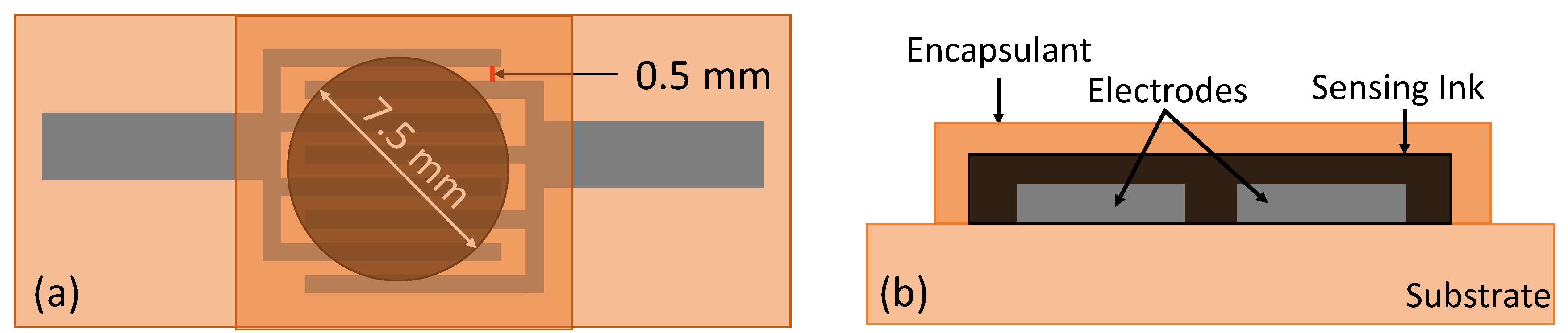
Figure 2.
a)- c) thermistor fabrication process d) High resolution optical microscopy image of printed thersmitor.
Figure 2.
a)- c) thermistor fabrication process d) High resolution optical microscopy image of printed thersmitor.
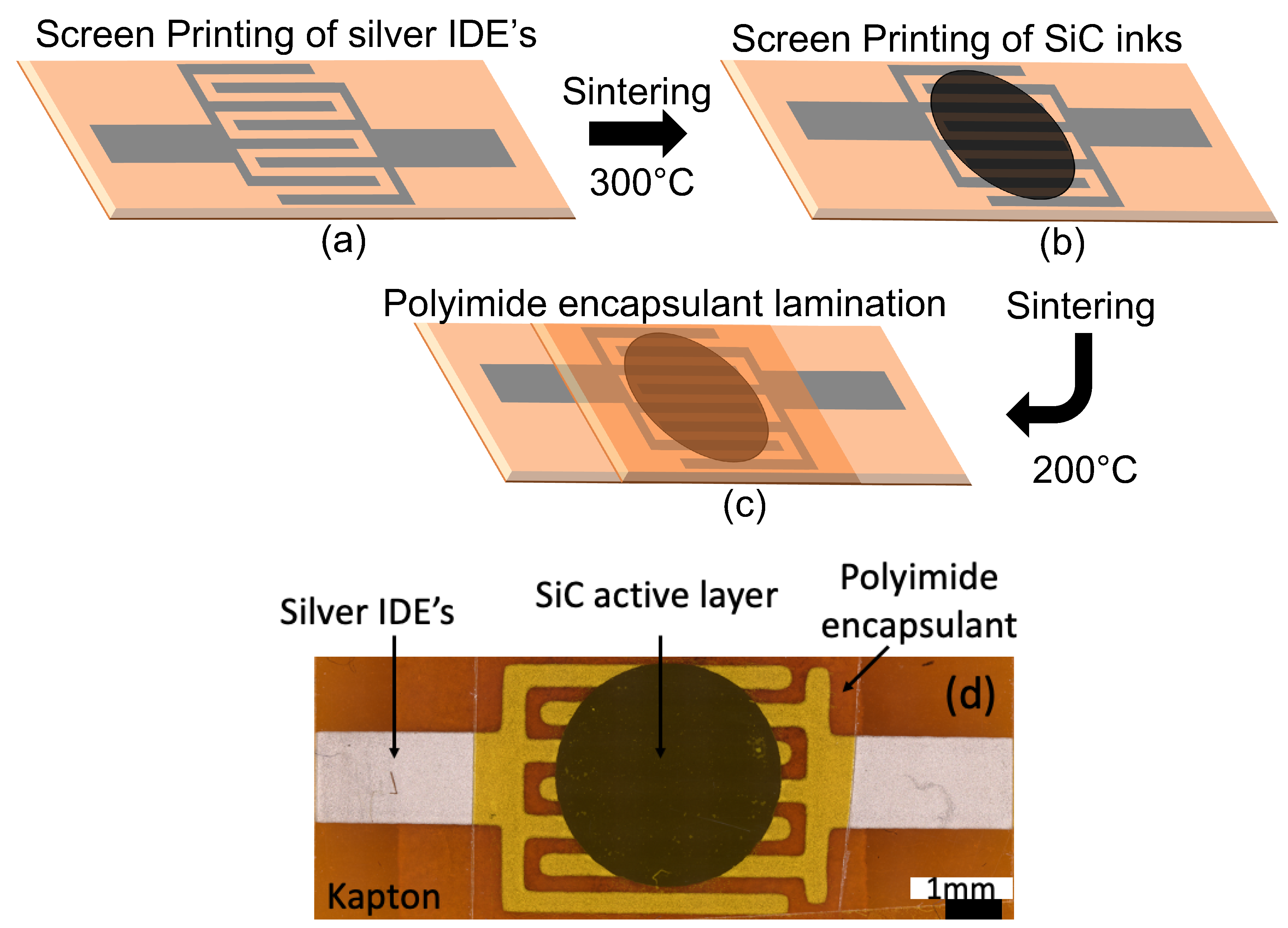
Figure 3.
Experimental setup.
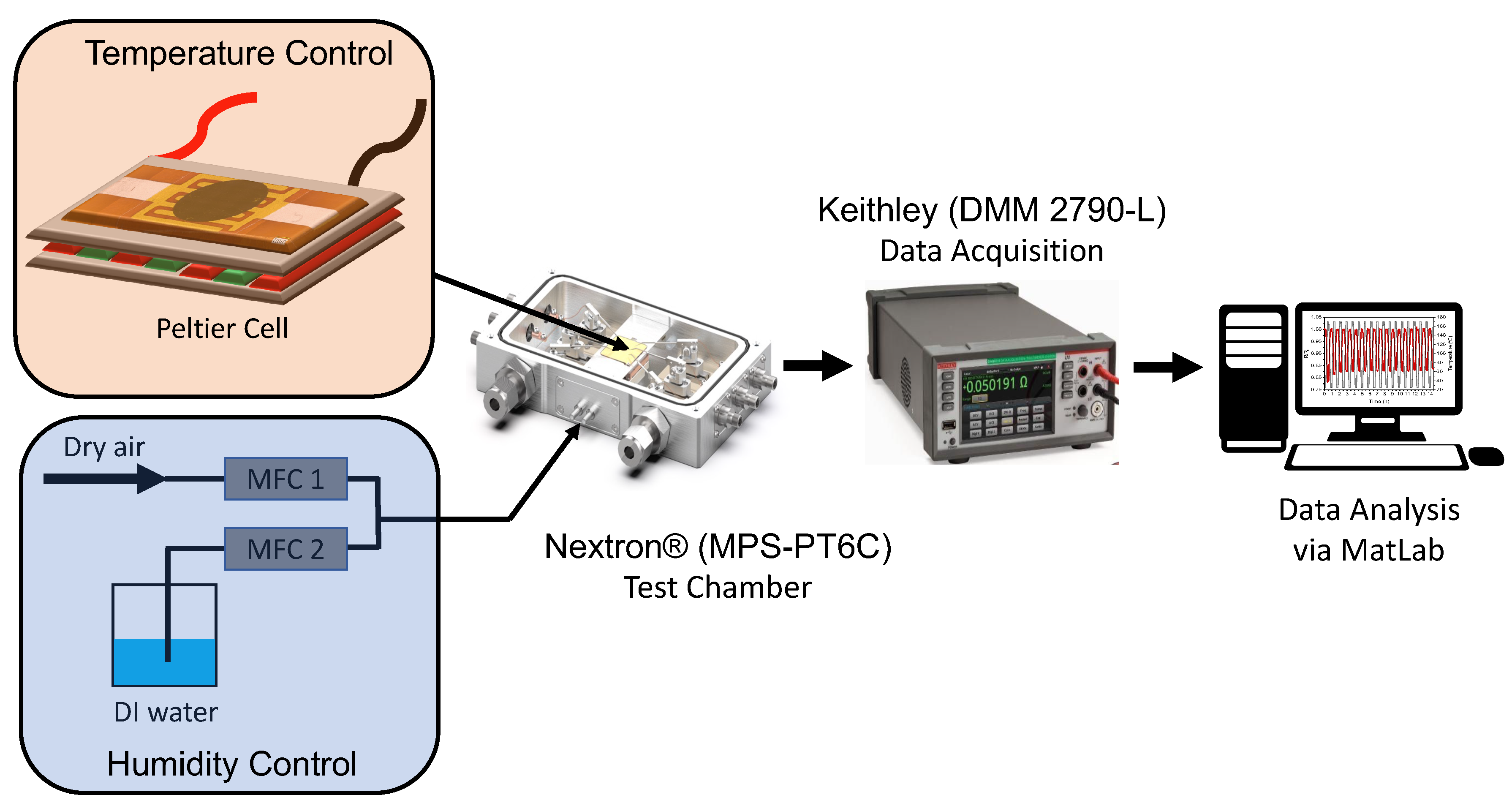
Figure 4.
Characterization of commercially sourced particles. a) XRD spectra, b) Raman spectra c) UV-VIS spectra with Tauc plot as inset to determine electronic band gap, d) SEM micrograph.
Figure 4.
Characterization of commercially sourced particles. a) XRD spectra, b) Raman spectra c) UV-VIS spectra with Tauc plot as inset to determine electronic band gap, d) SEM micrograph.
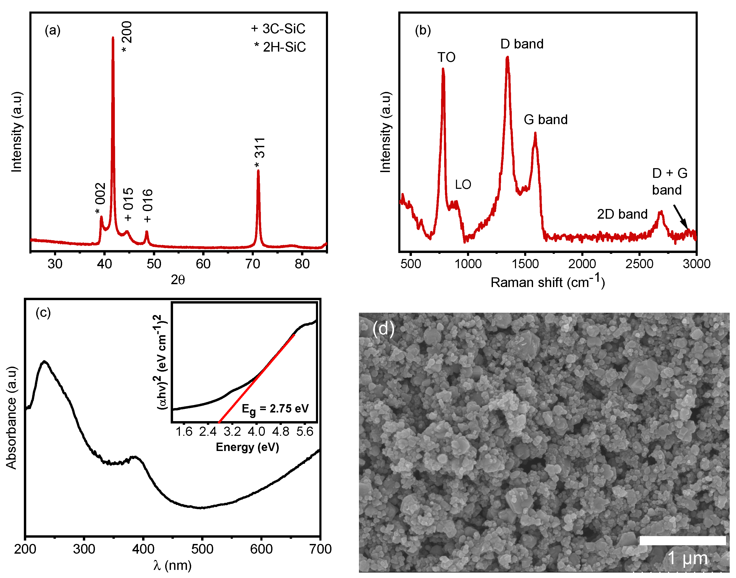
Figure 5.
EDX imaging of a) particles representing b) Si c) C and d) O species.
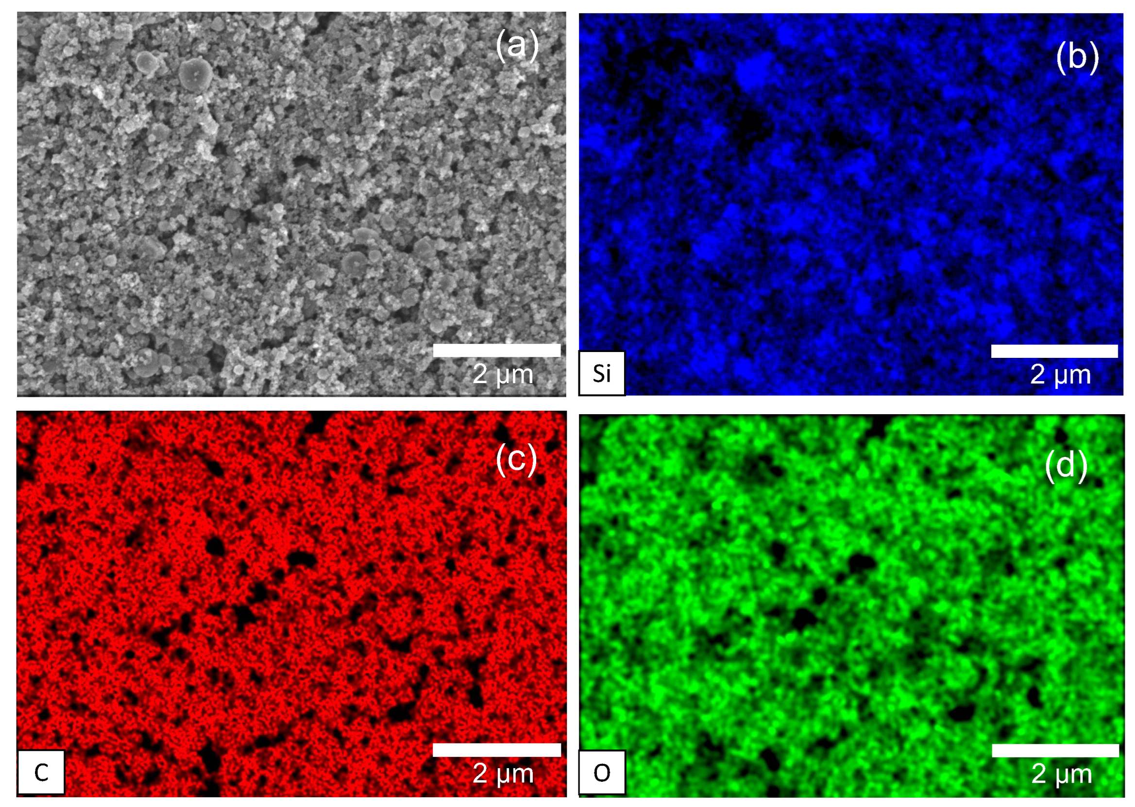
Figure 6.
a), b) TEM micrographs and c) SAED pattern of particles .
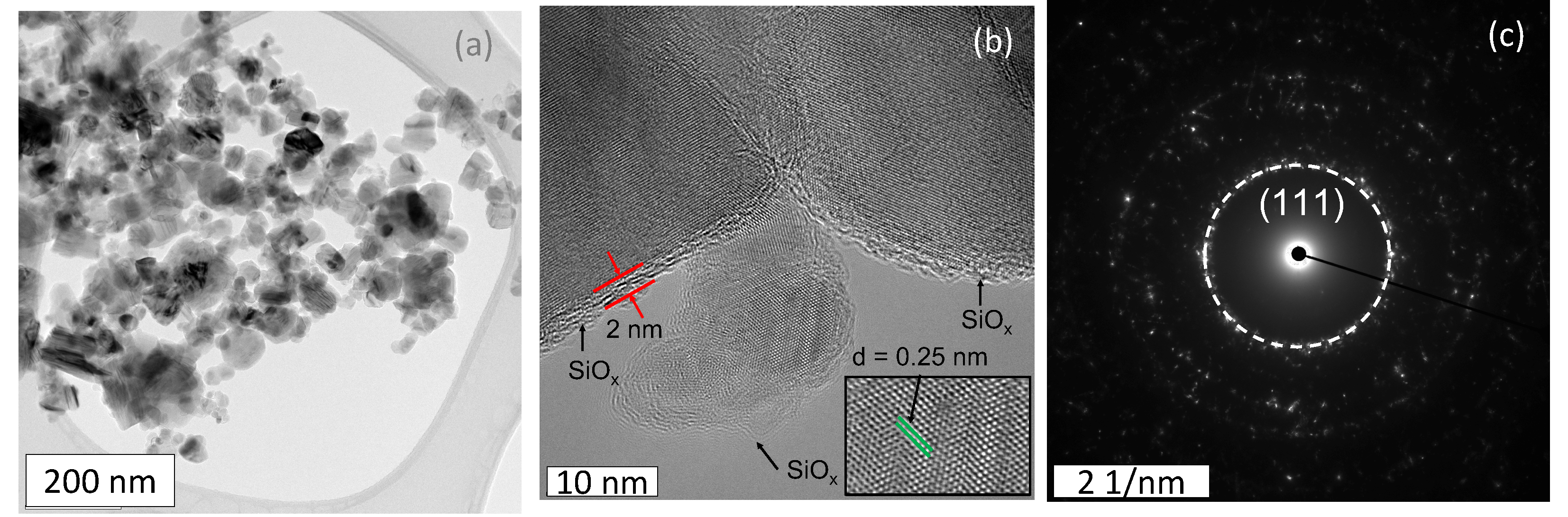
Figure 7.
a) Current-voltage characteristics and b) electrical conductivity of 30 wt.%, 35 wt.%, 40 wt.% thermistor inks.
Figure 7.
a) Current-voltage characteristics and b) electrical conductivity of 30 wt.%, 35 wt.%, 40 wt.% thermistor inks.
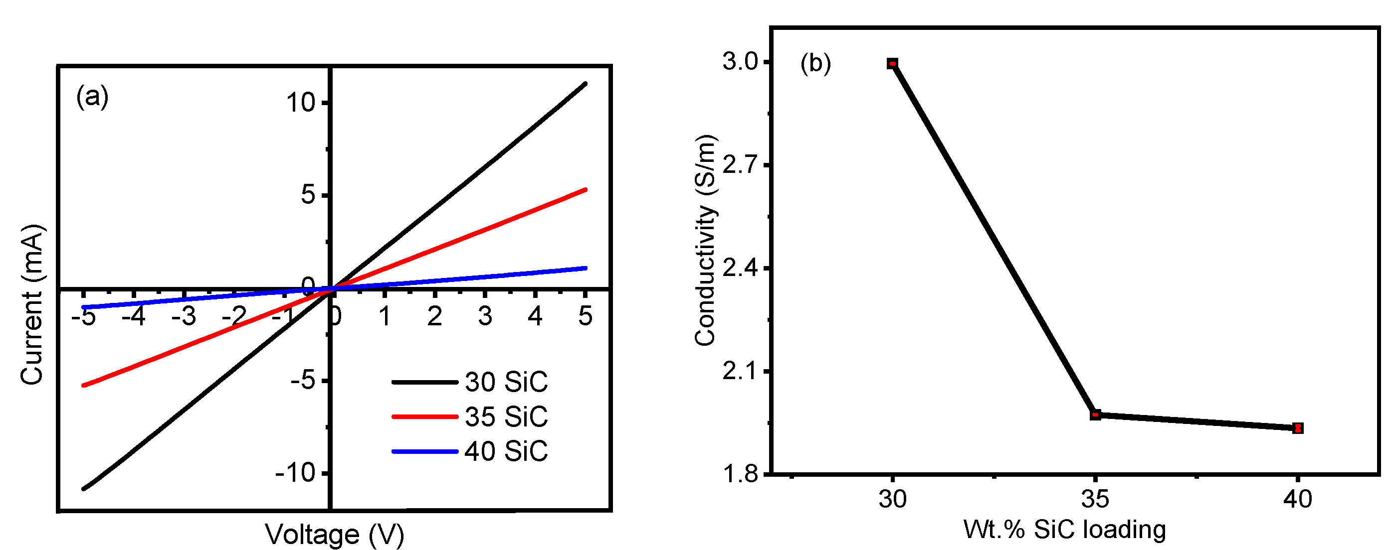
Figure 8.
SEM micrographs of a) and b) 30 wt.% c) and d) 35 wt.% e) and f) 40 wt.% thermistor inks.
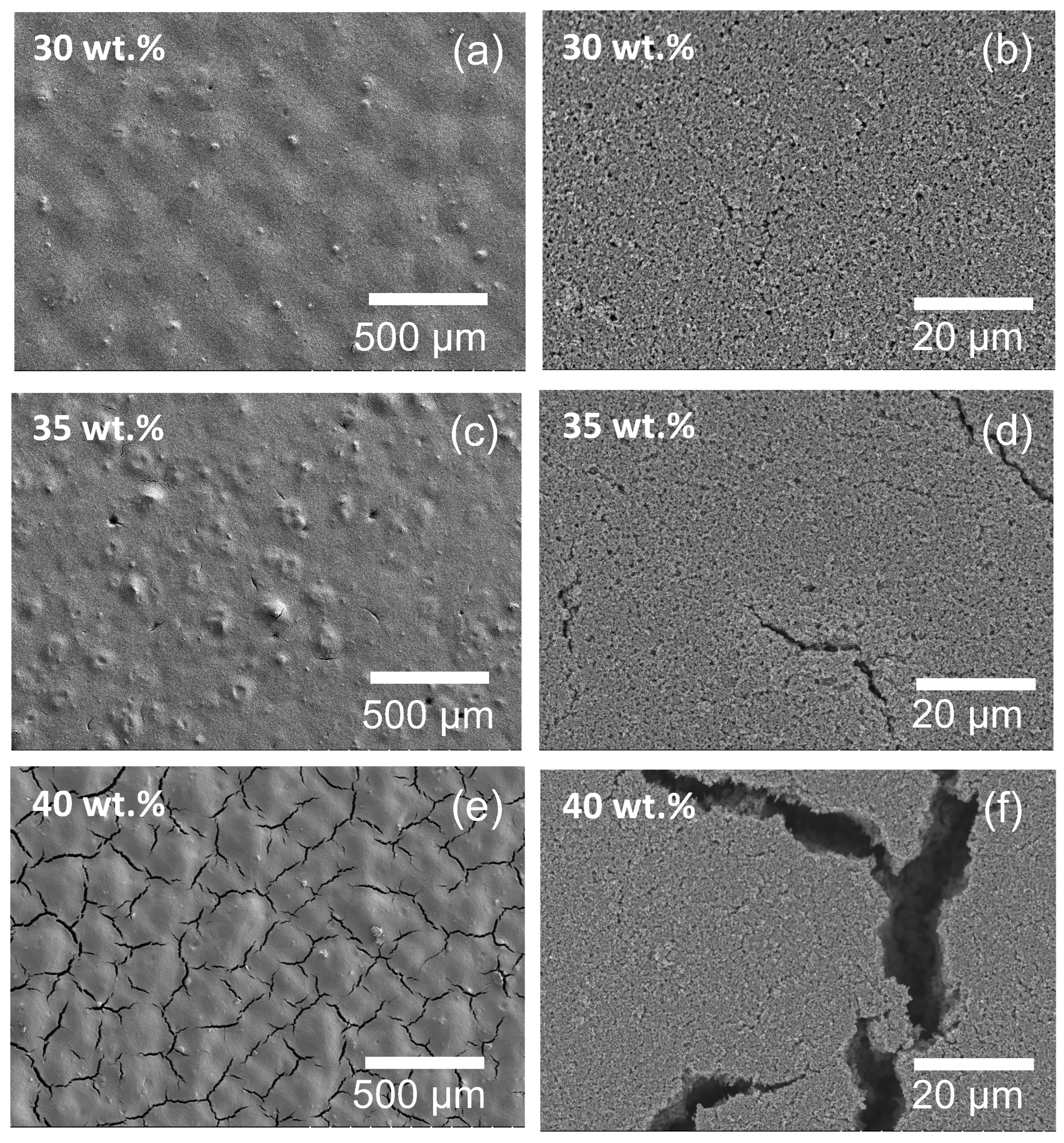
Figure 9.
a) Electrical resistance versus temperature of 30 wt.%, 35 wt.%, 40 wt.% thermistors b) long term cycling c) thermal stability d) humidity stability e) change in baseline resistance after bend testing and f) electrical resistance versus temperature plot after bend testing of 30 wt.% thermistor.
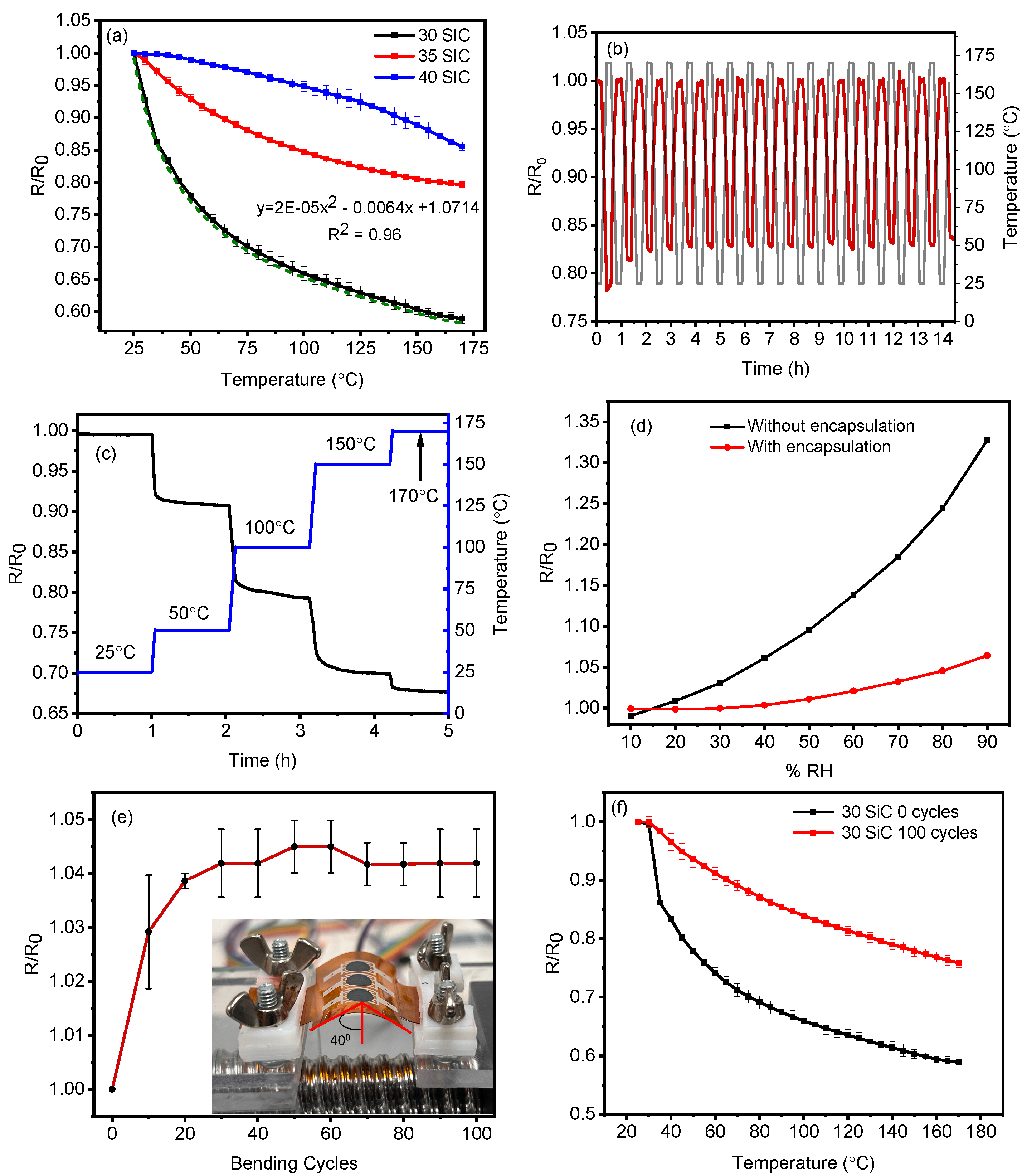
Figure 10.
Accuracy of printed 30 wt.% thermistor calculated via the Steinhart’s equation.
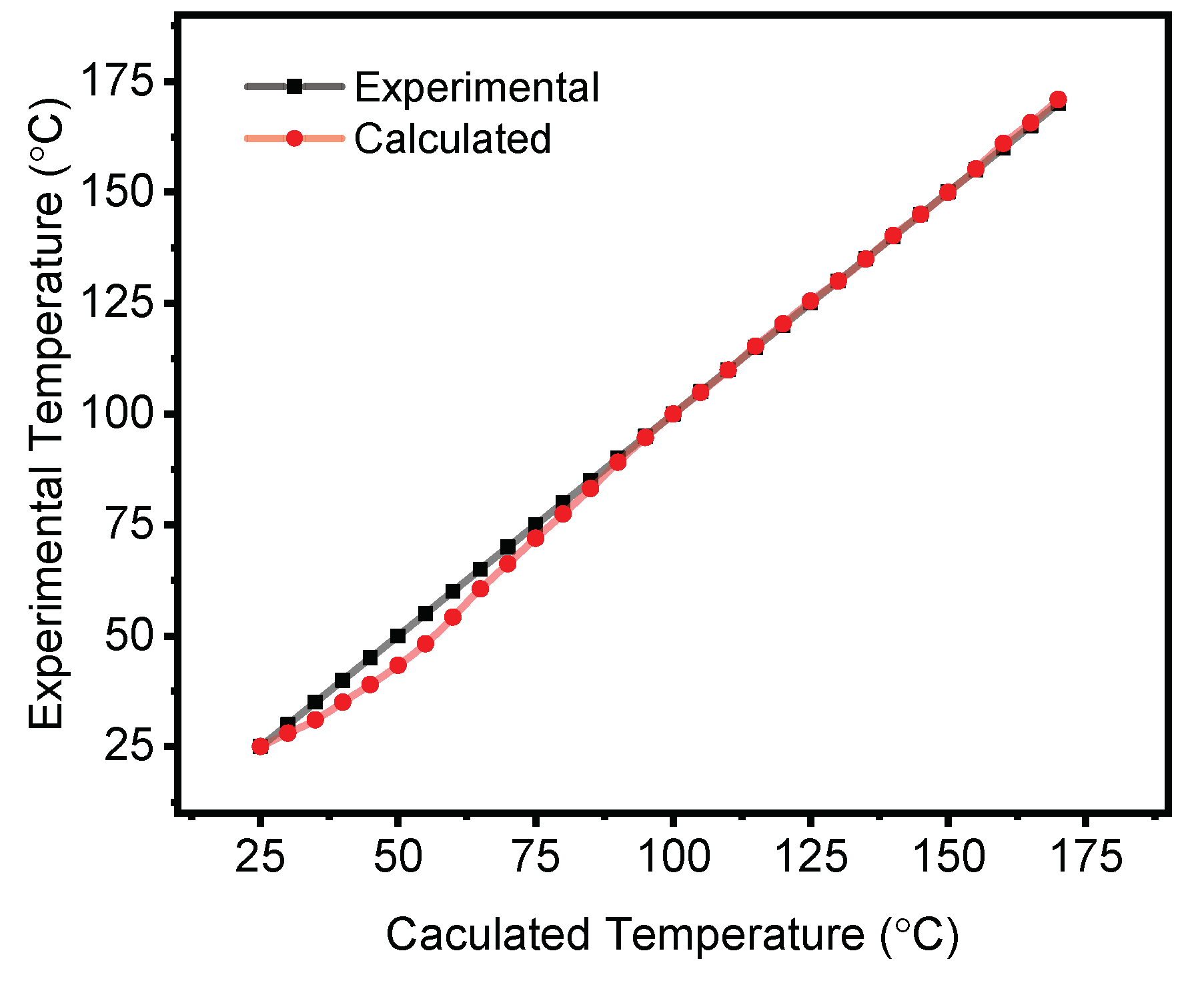

Table 1.
Electrical performance of various printed thermistor inks
| Ink Name | 3C-SiC wt% | PI resin wt% | TCR (%/°C) | Activation energy (eV) | Thermal index (K) |
|---|---|---|---|---|---|
| 30 | 70 | -0.556 ± 0.012 | 0.08 ± 0.001 | 502 ± 11 | |
| 35 | 65 | -0.227 ± 0.008 | 0.035 ± 0.001 | 205 ± 7.4 | |
| 40 | 60 | -0.157 ± 0.0068 | 0.025 ± 0.001 | 142 ± 6 |
Table 2.
State of the art of SiC based and printed thermistors
| Sensing material | Electrodes | Fabrication Method | Temperature Range | TCR | Reference |
|---|---|---|---|---|---|
| Silicon Carbide based thermistors | |||||
| On undoped wafer | , , Pt-Pd alloy | CVD | 25 °C - 400 °C | -7.9%/K | [41] |
| Anodic bonding on glass | Ni/Al | CVD | 300K - 600K | -13,000 ppm/K at 300K -3,000 ppm/K at 600K | [45] |
| n-type single crystal 21R- wafer | -- | magnetron sputtering | 77K - 450K | 10 times change in resistance | [44] |
| Doped unicrystalline SiC wafer | W (Tungsten) | welding | °C - 300 °C | 1.9%/°C | [82] |
| Polycrystalline CVD-SiC wafer | Pt-Pd alloy | Vacuum vapor deposition | 25 °C - 365 °C | -5.5%/°C | [83] |
| Printed Thermistors | |||||
| Carbon nanotubes | Screen printing | °C - 100 °C | -0.4%/°C | [16] | |
| PDMS + graphene | Copper wire | 3D printing | 25 °C - 70 °C | 0.008/°C | [84] |
| graphene oxide | Inkjet printing | 25 °C - 85 °C | -1.19%/°C | [85] | |
| + 3.5 wt% graphene | Ag | Screen printing | 25 °C - 170 °C | -0.961%/°C | [14] |
| Screen printing | 200K - 400K | -37,000 to -17,000 ppm/K | [86] | ||
| Screen printing | 25 °C- 170 °C | -0.556%/°C | This work | ||
Disclaimer/Publisher’s Note: The statements, opinions and data contained in all publications are solely those of the individual author(s) and contributor(s) and not of MDPI and/or the editor(s). MDPI and/or the editor(s) disclaim responsibility for any injury to people or property resulting from any ideas, methods, instructions or products referred to in the content. |
© 2024 by the authors. Licensee MDPI, Basel, Switzerland. This article is an open access article distributed under the terms and conditions of the Creative Commons Attribution (CC BY) license (http://creativecommons.org/licenses/by/4.0/).
Copyright: This open access article is published under a Creative Commons CC BY 4.0 license, which permit the free download, distribution, and reuse, provided that the author and preprint are cited in any reuse.


