
Submitted:
15 March 2024
Posted:
18 March 2024
You are already at the latest version
Abstract
The purpose of this study is to investigate the impact of the voltage drop of a three-phase voltage source inverter in driving brushless motors. This study also proposes an enhanced Field Oriented Control scheme that accounts for the inverter voltage drop enabling efficient drive at very low motor-speeds. Experimental results are provided to verify the theoretical study and the proposed control scheme.
Keywords:
motor control
; inverter modeling
; inverter voltage drop
; Field Oriented Control
; sensorless FOC
; flux observer
1. Introduction
Three-phase brushless motors have been in the forefront of industry for more than three decades due to their efficiency and low cost. During this period, the technological development of microcontrollers enabled the implementation of sophisticated control schemes for those motors that have also been widely applied in the industrial sector [1]. Sensor-less Field Oriented Control (FOC) has been one of those control schemes, probably being among the most popular when it comes to industrial motors. Compared to conventional control schemes, sensor-less FOC provides efficient motor drive with fast dynamic response and better motor controllability, low current total harmonic distortion (THD), and reduced losses [2,3]. However, when it comes to applications where controllability over very low motor-speed is required, the utilization of a high-performance microcontroller unit (MCU) might be a prerequisite; it is noteworthy that the minimum stability margin in many occasions could manifests at low speeds [4]. However, many residential and consumer electronic applications are sensitive to cost applications, and high performance MCUs cannot be easily afforded. Indicatively, household laundry motors with a gear ratio of 10 should work reliably down to 80 RPM, using conventional inexpensive microcontrollers, such as XMC13, XMC14 or PSoC4 from Infineon [5,6], STM32G0 family from ST Microelectronics [7], MSPM0G from Texas Instrument [8], and LPC800 series from NXP [9]. The constraints posed by the low bandwidth, along with the nonlinear voltage drops introduced by the driving system, particularly as highlighted later in this study the dead-time inverter voltage drop, can contribute to suboptimal controllability at low motor speeds. To tackle this problem, the voltage drops are typically modelled as an average voltage loss over the switching period and are then compensated directly within the abc-reference frame [10-13]. This compensation involves integrating them into the reference voltages generated by the FOC scheme, right before entering the Pulse Width Modulation (PWM) stage. Alternatively, the inverter voltage drop effect can be treated as a pulse shift error and directly compensated for in each PWM cycle [14, 15]. Some other works have proposed online compensation methods [16,17]. These methods are generally more intricate as they involve real-time estimation of the voltage drop, necessitating intensive computational processes. In addition to the online methods, some studies propose the self-commissioning characterization of the inverter during startup or when the motor is at a standstill [18-20]. In these works, the non-linearities of the inverter are estimated and stored in Look-Up-Tables (LUT) for subsequent compensation in the abc-reference frame. The techniques employed to generate these LUTs often involve current injection methods, such as applying a staircase current with a predetermined number of steps [19] or utilizing an increase-decrease current injection technique [20].
Although the above works target motor-drive applications, they do not consider low-end sensorless applications under dynamic conditions. Furthermore, achieving complete compensation of the inverter voltage drop is challenging due to nonlinearities like parasitic capacitances [15], temperature variations [18], DC-link voltage variations and so on. Therefore, as will be shown in this work, in low-end sensorless applications the direct compensation at abc-reference frame might prove inadequate, resulting in suboptimal performance at low speeds because of the insufficient compensation during dynamic conditions. Instead, it might be beneficial to address the compensation for the inverter voltage drop at the flux observer stage within the FOC framework where the system dynamics are better considered, rather than at the abc-reference and PWM stage. Such an attempt is made in [21], where a self-commissioning inverter characterization technique is proposed to identify and subsequently compensate the inverter non-linearities at the observer stage; a current is injected by the inverter during startup (when the motor back electromotive force (EMF) is zero) identifying and storing the inverter non-linearities. These identified nonlinearities are stored in a LUT for subsequent compensation. A similar attempt is made in the current work, where the voltage drops are compensated for at the flux-observer stage using a LUT. The key distinction from the work presented in [21] lies in the fact that in the current study the voltage drops are normalized within the αβ-reference frame offline (without any characterization process being involved) and pre-stored in a LUT. Subsequently, based on the sign of the inverter current, the voltage drops are retrieved from the LUT and employed within the αβ-reference frame at the flux-observer stage. While the proposed technique may not address all the nonlinearities of the inverter, it offers a straightforward solution that ensures effective motor control across a broad speed range. Additionally, this is a computationally inexpensive and fully compatible with low-cost microcontrollers solution, as it requires only a 64-Byte LUT to represent the inverter voltage drops in the αβ-reference frame as part of the FOC scheme. Moreover, when the motor reaches a certain speed, the impact of voltage-drops dilutes, therefore the controller disables the proposed voltage-drop compensation, transitioning into a conventional FOC controller. The entire FOC control scheme including the proposed methodology, has been implemented with an inexpensive 40 MHz 32-bit ARM® Cortex®-M0+ microcontroller of 64 kB, and 8 kB RAM, and has been experimentally tested for a low-end motor of 545W nominal power. Simulation and experimental results are presented to verify the effectiveness of the proposed methodology. The obtained results constitute this method as a promising solution for low-end Brushless motor drives.
To conclude, this paper studies the inverter voltage drop phenomenon in low-end motor drives. It also proposes a methodology to account for the voltage-drop to improve the controllability of brushless motors at low speeds. The proposed methodology can be easily implemented with inexpensive microcontrollers, such as ARM® Cortex®-M0 microcontrollers [5-9].
The rest of the paper is organized as follows: In Section 2, the system under study is described. In section 3 the principle of the FOC algorithm is presented. In Section 4 the voltage drop of the inverter is theoretically analyzed and modeled and the proposed methodology is presented. Section 5 and 6 present the simulation and experimental results, respectively. Finally, Section 7 concludes the paper and ideas for further applications are suggested.
2. System under Study
The system under study is illustrated in Figure 1. It is a conventional architecture of a low power motor drive system that comprises four subsystems/stages; the - mandatory - electromagnetic compatibility filter stage has been omitted from the description. The first subsystem is the Power Factor Correction (PFC) converter. The main task of the PFC is to provide a regulated output voltage and to improve the grid AC current Total Harmonic Distortion (THD). In this work a two-channel interleaved boost PFC converter has been used, maintaining a close to unity power factor (PF), low THD, and 400 V regulated output voltage, via a proper voltage regulation and power factor correction control scheme.
The second subsystem is the inverter, which is the subject of our work. In this work a three-phase two-level voltage source inverter (VSI), typical of such motor-drive applications has been used; the DC-input of the inverter is connected to the PFC subsystem, while its output is directly connected to the electric motor stator windings. The control of VSI is realized via a low-end MCU.
The MCU is the third subsystem. Typically, the MCU is a conventional low-end microcontroller that provides a PWM peripheral, along with an analog to digital (ADC) peripheral, and a serial communication peripheral. As previously noted, the MCU utilized in our work is a 40 MHz ARM® Cortex®-M0+ microcontroller equipped with 64 kB flash memory and 8 kB RAM. The ADC module boasts a 12-bit ADC channel, capable of handling a maximum conversion rate of 1.2 million samples per second, whereas the achieved Pulse Width Modulation (PWM) accuracy was measured at 10.29 bit.
The final subsystem is the driving unit, which encompasses a motor linked to a mechanical load; as this study focuses on applications that require low-end motors, it includes residential laundry appliances and air-compressors.
3. FOC Description
This section aims to describe briefly the FOC control-scheme. Figure 2 illustrates the typical block diagram of a sensorless FOC [3], where the term sensorless refers to the method of estimating the motor speed and position. In other words, the position (θest) and speed (nest) of the rotor are not directly measured but estimated/calculated. It is also worth noting that according to Figure 2, FOC enables the control of the motor speed directly from the q-component of the motor current, while the d-component of the motor current is directly related to the flux that is produced by field windings. Severing the direct relationship between motor speed and the d-component of motor current yields significant advantages in terms of control. In this study, an initial DC current is injected to the motor stator windings during startup, thereby orienting the rotor to its initial position. This approach effectively decouples the motor control parameters.
In the current work, the position (θest) and speed (nest) are estimated with the aid of a reduced order flux observer, akin to the one described in [22]. This method provides a robust low-complexity solution with good dynamic control and wide speed range operation, even in the presence of parameter variations and measurement noise. The flux observer receives as input the motor current and the VSI reference voltages at αβ-reference frame, while it generates as an output the estimated motor speed and position. The motor speed is controlled via a Proportional Integral (PI) controller. The task of the PI controller is to maintain the estimated speed at speed reference value nref. The output of this PI controller is used as the input reference q-component of the motor current. The measured and reference q-components are fed to a second PI, the output of which is used to generate the reference value of the q-component of the inverter reference voltage. When flux weakening is not engaged, the reference value of the d-component of the motor current is set to zero (0.0). The d-component is controlled via a third PI controller, the output of which generates the d-component of the VSI reference voltage. The generated dq-components of the voltage reference of VSI are transformed back to abc quantities with the aid of the inverse Park and inverse Clark transformations. These time variant voltage quantities are considered as the output of the FOC control scheme. They are fed to the PWM module of the MCU along with the DC-link voltage to generate the appropriate switching pattern that will drive the insulated-gate bipolar transistors (IGBTs) of the VSI; in the current work the modulation strategy that has been used is based on the bipolar PWM, while a third harmonic injection is, afterwards, used to boost the DC-link utilization level. Once the switching pattern is applied to the IGBTs, the inverter should generate the desirable AC voltage to drive the motor.
It is also noted that in Figure 2 the FOC block diagram incorporates the Flux Weakening component, as well. However, since the analysis in this paper focuses on low motor speeds, the following discussion will omit the explanation of the flux-weakening part. For a more comprehensive understanding of flux-weakening, readers may consult the relevant references [23, 24].
4. Inverter Voltage Drop Modeling
4.1. Basic Analysis of Inverter Voltage Drop
As mentioned in the Introduction, when the FOC algorithm tries to control the motor at very low speeds, the voltage that is generated by the inverter is in the same order of magnitude with the inverter voltage drop, significantly affecting the estimated speed and the estimated position of the rotor. This results in a poor performance of the flux observer and eventually of FOC. Indeed, for typical sensorless low-end applications, the inverter voltage drop is the bottleneck for low-speed control. In this section we are going to elaborate this problem by analyzing the VSI output voltage and the voltage drop that occurs by the non-ideal characteristics of the inverter and we will propose a solution to increase motor controllability at low speeds.
Due to intrinsic characteristics of the IGBTs and diodes as well as due to the switching modulation pattern of the inverter, there is a voltage drop across the inverter output. This drop comes primarily from:
- IGBTs/diodes conduction & switching losses (such us IGBTs forward voltage, and on state resistance, diodes forward voltage-drop).
- PWM dead-time.
The voltage drop that comes from IGBTs/diodes conduction & switching losses depends on the motor current and their bespoken inherent characteristics, while the voltage drop that comes from the PWM dead-time depends on the dead-time duration and the level of the DC-link voltage. For single phase applications, where the DC-link voltage of VSI is typically boosted around 400V, the PWM dead-time is the predominant factor of VSI voltage drop.
With the aid of the circuit in Figure 3, we can gain a better understanding of the physical representation of the inverter output voltage and the inverter voltage drop. Each leg of the inverter generates a voltage with respect to node ”o” (i.e. vxo) and a voltage with respect to node “m” (i.e. vxm), where “x” denotes the inverter phases, a, b, and c. The output voltage of the inverter, hereafter vxo, is dictated by the switching pattern of IGBTs and the DC-link voltage; as already noted, the DC-link of single-phase applications is typically regulated by the previous stage (typically via the PFC) to around 400V. The switching pattern of the inverter is dictated by the modulation strategy (PWM, space vector modulation, discontinuous PWM, etc.), the reference voltage quantities vsa,ref, vsb,ref, vsc,ref, (which are generated by the FOC scheme), and the peripheral configurations of the MCU (PWM resolution, single-edge/symmetrical-mode, etc.). Although FOC generates in principle symmetrical sinusoidal reference quantities, the inverter output voltage, vxo, and the voltage that is applied at the motor winding, hereafter, vxm, contains high frequency components, because of the modulation switching pattern. Due to the VSI topology and the modulation strategy, a high-frequency voltage is also generated at vmo. The relationship between vxo, vxm, and vmo is defined in the following equation:
To exclude the high frequency ripple from our analysis, we will adopt a switching-average model [25]. Equation below, where “ * ” stands for switching average quantities, demonstrates the mathematical approach behind the switching-average modeling:
Applying the switching average approach to eq.1, we obtain the following expression:
Assuming the case of an ideal inverter without voltage drop, 𝒗𝒙𝒐 can be rewritten as:
, where dx(t)* (0 ≤ dx(t)* ≤ 1) denotes the percentage of the switching period at which the upper IGBTs are turned-on. dx(t)* is the control input signal to our model, the value of which is dictated by the FOC controller.
In the case where the inverter is ideal, the sum of vao(t)*+ vbo(t)*+ vco(t)* is zero (0.0), as FOC generates in principle three-phase symmetrical reference voltages, therefore:
Concluding, in case of dead-time free operation, the switching average voltage that is applied at the windings of the motor (vxm) is controlled directly by the reference voltage that is generated by the FOC.
When the inverter is not ideal, the sum of voa(t)*+ vob(t)*+ voc(t)* is not zero (0.0), because vxo(t)* also includes the inverter voltage drop. At low motor speeds, the motor driving voltage is low, and the dead-time period of the inverter becomes the main source of voltage drops. Dead time is a well-known concept in power conversion systems according to which the switching elements that belong to the same inverter leg must simultaneously turn off - for a certain period - before each switching transition, to avoid shorting the inverter.
To understand the rationale behind the distortion in the generated voltage, it is essential to initially delve into the influence of dead time on the inverter output voltage, vxo. By examining Figure 4 and Figure 5, the discernible impact of asymmetric (keeping the turn-off edges intact) dead-time on inverter voltage vxo* becomes evident.
Applying circuitry analysis in Figure 3 and considering the current flow analysis in Figure 4 and Figure 5, we reach the following equations regarding the inverter output voltage:
If the current of x-phase is positive:
If the current of x-phase is negative:
As we observe, vxo(t)* contains an additional part, which depends on the direction of the corresponding phase current. That additional part is hereafter named as inverter voltage drop. That part is uncontrolled, and it depends on the DC-link voltage, the PWM dead-time, the PWM frequency, and the direction of the corresponding phase-current; the resistance of switching element (rds-on), and non-linearities such as parasitic capacitance [15] and switching elements junction-temperature [18] also affect the voltage drop, however they are not considered in this study. To distinguish the uncontrolled part from the inverter output voltage that we can control via the FOC, we will use the following two conventions. The term vxo,FOC(t)* stands for the component that is controllable via the FOC scheme, and the term vxo,drop(t)* stands for the uncontrolled voltage drop component:
, the sign of which depends on the x-phase current of the motor, iSx(t).
Based on eq.9, the magnitude of inverter voltage drop depends on the PWM period, the PWM dead time, and the inverter DC voltage. As those parameters are typically fixed for each application, the following constant can be used to benchmark the inverter voltage drop:
Having defined vxo(t)*, we can define the voltage across the motor winding as:
As FOC generates symmetrical three-phase voltages, eq. 11 is rewritten as:
Like vxo(t) *, the switching average voltage that is applied across the motor winding, vxm(t)*, consists of two parts: a part that is directly controlled by FOC and an additional part, which depends on inverter voltage drop, that cannot be directly controlled. This additional part will be hereafter named as motor winding voltage drop, denoted as vxm,drop(t)*:
Assuming that the motor is fed with symmetrical sinusoidal three-phase currents, the value of vao,drop(t)*+ vbo,drop(t)*+ vco,drop(t) equals to ±Vdrop, where the sign depends on the signs of the phases current (Table 1):
Concluding, by applying eq. 14 to eq. 9 and eq. 13, we derive the normalized values of inverter and motor winding voltage drop, vao,drop(t)* and vam,drop(t)*, respectively. For phase-a, those values are shown in the table below and plotted against time in Figure 6, using Vdrop in eq. 10 as the base value and assuming that the motor is fed with the arbitrary selected symmetrical sinusoidal three-phase currents of the top graph of Figure 6. Similar values can be readily derived for the remaining b & c phases.
4.2. Voltage Drop: Modeling in aβ and dq-Synchronous Reference Frame
This subsection aims to represent the voltage drop in αβ0 and dq0 – reference frames. This representation is very useful, as it will be used later to integrate them in the existing FOC scheme (Section 5).
Typically, the dq0-transformation that is used in FOC schemes is the amplitude-invariant version. Also, the d-component is usually aligned with the a-phase of the inverter reference voltage. The amplitude invariant dq0-transformation - which aligns the a-phase with the d-component- is achieved by using the well-known matrix in eq. 15. For q-component alignment, alignment with b/c-phases, or power-invariant transformation the appropriate matrixes should be utilized; however, the subsequent analysis remains valid.
Similarly, for a-phase alignment the amplitude invariant αβ0-transformation is achieved by using the matrix below:
For the derivation of the αβ0 and dq0 - components of the motor winding drops vxm,drop(t)* we use as [a;b;c] input, the quantities [vam,drop(t)* ; vbm,drop(t)* ; vcm,drop(t)*], whereas for the αβ0 and dq0 -transformation of inverter voltage drops vxo,drop(t)* we use as [a;b;c] input, the quantities [vao,drop(t)* , vbo,drop(t)* vco,drop(t)*]. After algebraic computations we end up to the following conclusions:
Figure 7 illustrates the αβ0 and dq0 components of inverter and motor winding voltages, considering that the motor is fed with the arbitrary selected symmetrical sinusoidal three-phase currents of the top graph of Figure 7. Please note that the 0-component of winding motor voltage drop is zero (0.0) both in αβ0 and in dq0 transformations, while the 0-component of inverter voltage drop is a square waveform with a frequency of 3 times the fundamental frequency.
Finally, the dq-components of the inverter output voltage, and the motor winding voltage drop consist of both a dc part and an alternating part. The former represents the voltage-drops in grid-frequency, while the latter represents the high frequency ripple drop (6 times the fundamental frequency). The dq and αβ components that refer to the motor windings are the ones that must be considered within the FOC control scheme. In particular, the αβ-components are the ones that have been inserted to the flux observer of Figure 2 to account for the inverter voltage drop. Next paragraph describes the proposed methodology.
4.3. Voltage Drop: Insertion in FOC aβ-Reference Frame
Substituting the [a;b;c] components of eq. 16 with the obtained values of vxm,drop(t)* ;and vxo,drop(t)* of Table 1, we reach to the following LUT:

Table 2.
αβ - LUT.
| vam,drop(t)* | vbm,drop(t)* | vcm,drop(t)* | iSa(t) | iSb(t) | iSc(t) | ||
|---|---|---|---|---|---|---|---|
| +2/3 Vdrop | +2/3 Vdrop | -4/3 Vdrop | +2/3 Vdrop | +2/√3 Vdrop | - | - | + |
| -2/3 Vdrop | +4/3 Vdrop | -2/3 Vdrop | -2/3 Vdrop | 0 | + | - | + |
| -4/3 Vdrop | +2/3 Vdrop | +2/3 Vdrop | -4/3 Vdrop | -2/√3 Vdrop | + | - | - |
| -2/3 Vdrop | -2/3 Vdrop | +4/3 Vdrop | -2/3 Vdrop | -2/√3 Vdrop | + | + | - |
| +2/3 Vdrop | -4/3 Vdrop | +2/3 Vdrop | +2/3 Vdrop | 0 | - | + | - |
| +4/3 Vdrop | -2/3 Vdrop | -2/3 Vdrop | +4/3 Vdrop | +2/√3 Vdrop | - | + | + |
The proposed methodology is depicted in Figure 8. The DC-link voltage, dead-time interval, and switching period are used to calculate the Vdrop magnitude. The dead-time interval and switching period represent constant parameters primarily contingent on the application. On the other hand, even though the DC-link voltage is maintained at a fixed value through regulation by the PFC, it might exhibit fluctuations due to the finite control bandwidth of the PFC and the modulation of the inverter. However, in three-phase systems, the fluctuation of the DC-link voltage is minimal and is largely mitigated using electrolytic capacitors at the inverter input. Given the gradual nature of DC-link voltage dynamics, the update frequency of Vdrop can be set quite low, such as 10 Hz.
The estimated Vdrop and motor current are then employed to derive the αβ-components of the voltage drop. Subsequently, these components are combined with the αβ-components of the inverter reference voltage and fed into the flux observer block. As it will be demonstrated later, the incorporation of the voltage drop into the flux observer block yields benefits as the observer dynamic response is accounted more effectively.
5. Simulation Results
In this section simulation results are presented, where our proposed enhanced FOC methodology has been used to drive a 4-pole pairs brushless motor. The system has been simulated in Matlab-Simulink 2021a®, omitting the PFC stage and electromagnetic compatibility (EMC) filter. The chosen VSI topology employs a three-phase B6 configuration, as illustrated in Figure 1. The input voltage of the inverter is set fixed to 400V. The inverter as well as the motor characteristics that have been used for the simulation are listed in the table below.
Table 3.
Simulation System Parameters.
| PFC & VSI characteristics | Value | Motor characteristics | Value |
|---|---|---|---|
| Inverter dc-link volt. (V) | 400 | Motor nominal speed (rpm) | 6,000 |
| VSI Switching Freq. (kHz) | 16 | Motor maximum speed (rpm) | 7,000 |
| Dead-time (us) | variable | Motor winding Inductance (mH) | 16 |
| Dead-time utilization | asymm. | Motor winding resistance (Ω) | 2.5 |
| Modulation | SV-PWM | Motor Pole Pairs | 4 |
| Deactivation speed of proposed methodology (rpm) | 1,000 | BEMF constant (voltage1/rpm) | 0.028138 |
1Peak phase voltage.
5.1. Proposed Voltage Drop Compensation Scheme
Figure 9 demonstrates the positive impact of our proposed methodology. Specifically, it showcases a scenario where the motor is commanded to achieve 82 rpm from a standstill position under maximum loading. The simulation comprises three cases:
- In the top graph, the system operates ideally with no dead-time introduced.
- In the middle graph, the system is non-ideal, featuring a 2 us dead-time but without any compensation method.
- In the bottom graph, the system is non-ideal and incorporates a 2 us dead-time along with the application of our proposed compensation method.
Figure 9.
Dead-time impact around motor start up; inverter phase current waveforms (without any compensation the motor fails to start-up).
Figure 9.
Dead-time impact around motor start up; inverter phase current waveforms (without any compensation the motor fails to start-up).
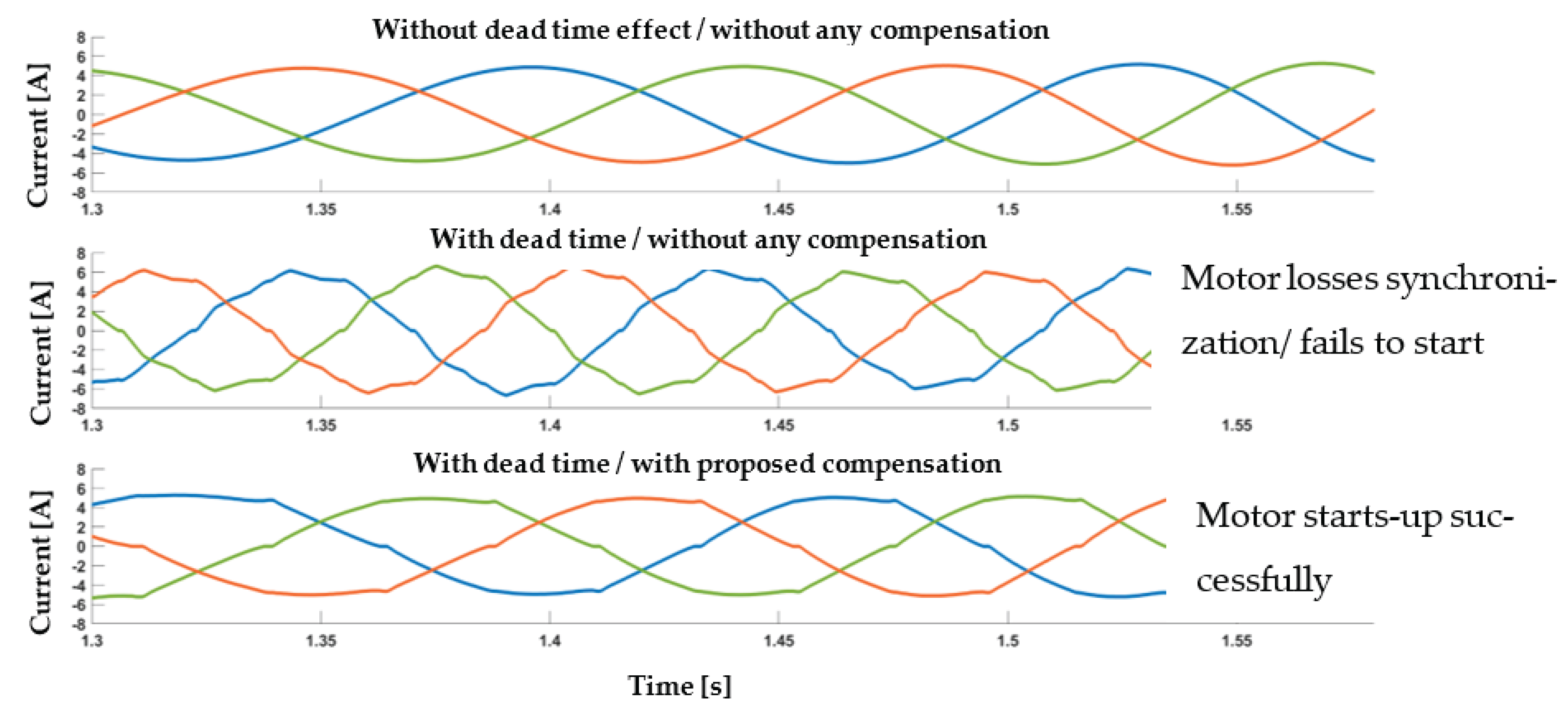
It is evident that without any compensation, the motor fails to start-up under realistic dead-time values.
5.2. Comparison on Voltage Drop Compensation Location
In Figure 10, the FOC response is depicted for different cases of dead-time, with compensation applied to the voltage drop at the abc-reference frame at the PWM stage. The simulation scenario showcases the motor being commanded to reach 82 rpm from a standstill position while experiencing maximum loading. These results are based on the system parameters outlined in Table 3. As evident from the presented results, the flux observer encounters significant fluctuations even with a dead time of 1.5 us, whereas the motor fails to start-up at all for dead times exceeding 1.9 us.
On the other hand, the outcomes of employing the proposed methodology for the above simulation scenario are depicted in Figure 11. Notably, the flux observer demonstrates significantly reduced fluctuations, while the motor is able to start-up and sustain the speed of 82 rpm, even with a high dead time of 2 us.
Lastly, Figure 12 provides a comparative overview of motor controllability at low rpm. The comparison is made under conditions of a 2 us dead-time, for three scenarios: a) without any compensation, b) compensation at the abc-reference frame, c) and the proposed methodology involving voltage drop compensation at the αβ-reference frame. The superior performance of the proposed methodology is evident based on the showcased results.
5.3. Enhanced FOC Validation over the Entire Motor Speed Range
Finally, results are presented where the proposed enhanced FOC is used to drive the system over the entire speed range (0 – 7,000 rpm). The motor is accelerating at 560 rpm / s till reaching 7,000 rpm. Flux weakening is engaged at around ~6,000 rpm. The proposed methodology is disengaged after the motor exceeding 1,000 rpm. When the motor reaches its maximum speed, it is commanded to decelerate down to 82 rpm. The motor deceleration is again set at 560 rpm / s. When the motor speed drops below 1,000 rpm, the proposed methodology is engaged. Finally, the motor reaches and maintains the desired speed (82 rpm) after approximately 12.5 s. Figure 13 showcases the above scenario, including two subfigures zooming-in around the start-up and the final commanded speed of the motor.
Lastly, we present results where the proposed enhanced FOC is utilized to drive the motor across its entire speed range (0 – 7,000 rpm). The motor initially accelerates at a rate of 560 rpm/s until it reaches 7,000 rpm. Beyond 1,000 rpm, the proposed voltage drop compensation is deactivated. Flux weakening comes into effect at around 6,000 rpm and remains engaged until the motor speed falls below this threshold during the deceleration phase. After the motor reaches its maximum speed, it maintains this speed for ~10 seconds and then it is commanded to decelerate down to 82 rpm, with the deceleration rate set again at 560 rpm/s. The proposed methodology is reactivated as the motor speed drops below 1,000 rpm. The motor effectively attains and sustains the target speed of 82 rpm for approximately 7.5 seconds. Figure 13 provides an illustration of the described scenario, encompassing two subfigures that provide a closer view of the motor startup and the final commanded speed.
6. Experimental Results
This section presents some experimental results of an actual motor drive system. A test-bench has been constructed to validate the proposed voltage drop compensation method. The entire experimental set-up is depicted in Figure 14. It consists of the following subsystems (as described in the Introduction):
- The EMC filter.
- The PFC.
- The VSI.
- The MCU.
- The Driving system.
For this study, the SECO-1KW-MCTRL-GEVB evaluation board provided by onsemi has been utilized [26]. This board incorporates both the PFC and VSI stages, along with the electromagnetic compatibility filter. The PFC stage comprises a single-phase passive rectifier and a 2-channel boost converter. Conversely, the VSI employs a traditional 3-phase B6 configuration, common in motor applications. The VSI is built using the Intelligent Power Module (IPM) AND9390/D, a specialized integrated circuit (IC) tailored for three-phase motor applications by onsemi [27]. The board is also equipped with a convenient connector designed for external control of the VSI IGBT gate drivers. The complete layout of the board, encompassing the electromagnetic compatibility filter, is illustrated below. Positioned at the bottom of the evaluation board, one may notice the control board housing the MCU.
Regarding the MCU, a low-end ARM® Cortex®-M0+ microcontroller has been used. This utilized MCU has a flash memory of 64 kB, and a 40 MHz clock. It also comes with Direct Memory Access (DMA), a PWM peripheral, a 12-bit 1.2 M samples/sec ADC peripheral, and Timer modules, which have been used for the FOC implementation. The MCU board is also outfitted with suitable connectors designed to interface with the evaluation board. As shown in Figure 15 (right photo), the MCU board is affixed to the underside of the evaluation board.
Finally, regarding the driving system, two mechanically coupled 545 W 4 pole-pair brushless AC machines from Bosch have been used, where one machine is operating as motor and the other as generator (see Figure 14). The generator is loaded via a - three-phase - variable resistive network, behaving as an equivalent variable mechanical load. Table 4 provides an overview of the foremost technical specifications of the system.
6.1. Start-Up to Low-Speed Validation
This section is dedicated to assessing the effectiveness of our proposed method under low-speed operation. Indeed, when the motor operates at low speed the effect of the voltage drop is critical. Also, the controller encounters the most significant challenges at low speed, specifically when the motor is commanded from a stalled position to achieve minimal speed under the influence of maximum loading. As such, Figure 16 showcases a scenario where the motor is stalled and commanded to reach 82 rpm under heavy loading conditions. This is reflected by the shorting of the three-phase resistor network, simulating a heavily loaded operational state.
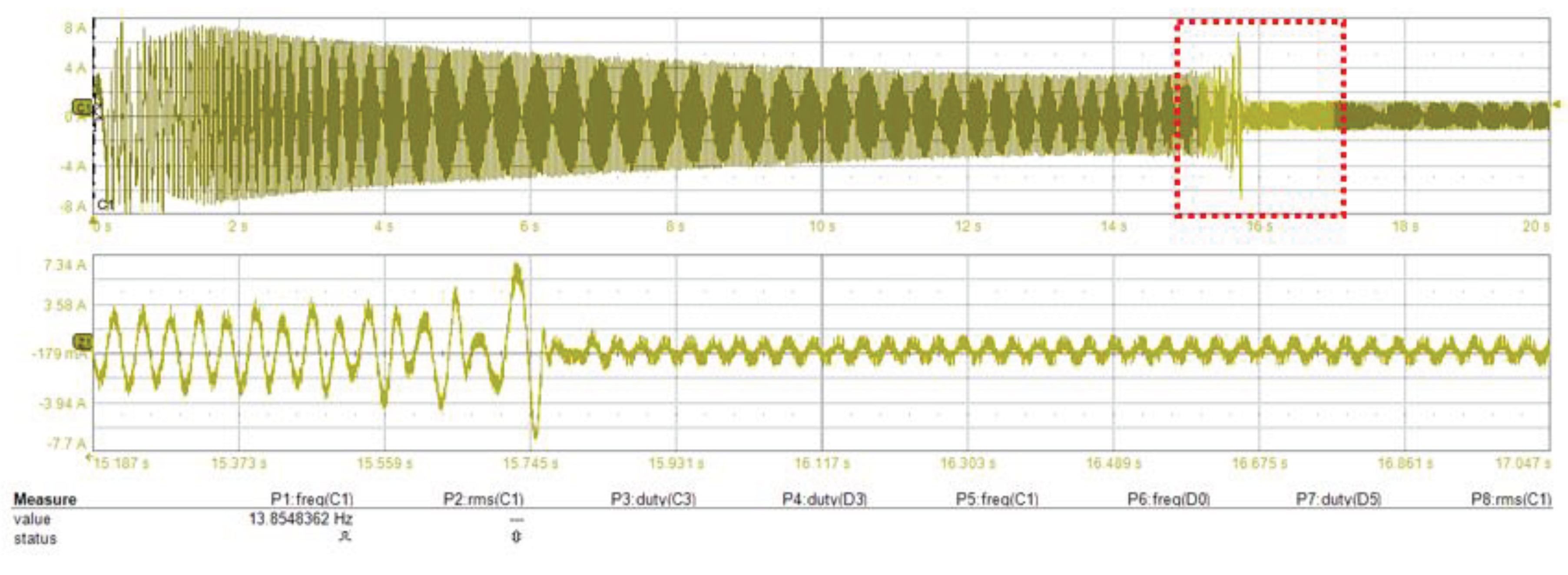
The scenario described above, involving the motor being in a stalled position and commanded to reach 82 rpm, was replicated without applying our proposed compensation methodology. Figure 17 and Figure 18 provide insight into the motor current. As evident, the motor loses synchronization and is unable to startup.
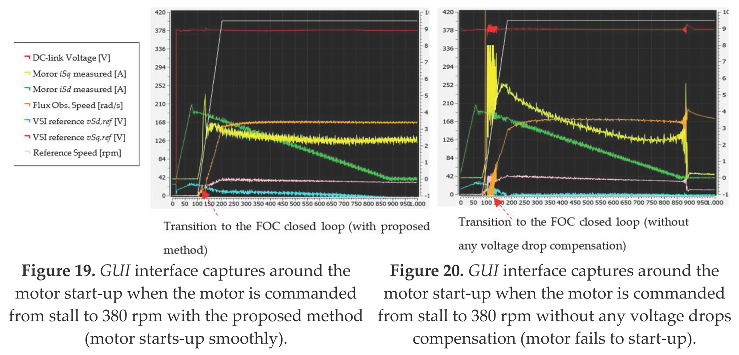
Finally, Figure 19 and Figure 20 presents results from the graphical user interface (GUI) that has been used during the experiment. Figure 19 provides insight into some crucial controller parameters when the motor is at standstill and commanded to reach 380 rpm under maximum loading, employing our proposed methodology. The same scenario is replicated without our methodology, shown in Figure 20. In the absence of compensation, the motor fails to initiate when dead-time is introduced.
Figure 16.
Standstill to 82 rpm with proposed method, top) Inverter phase current during the motor start-up, bottom) zoom in around 0.86s.
Figure 16.
Standstill to 82 rpm with proposed method, top) Inverter phase current during the motor start-up, bottom) zoom in around 0.86s.
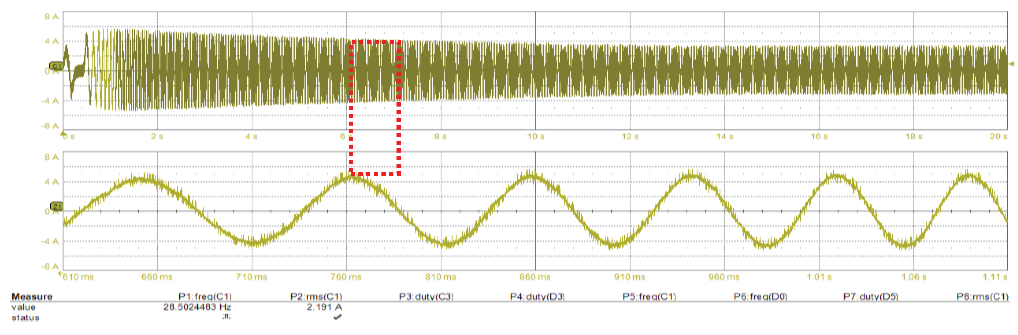
Figure 17.
Standstill to 82 rpm without any voltage drop compensation (motor fails to start-up), top) Inverter phase current during start-up (2 s / div), bottom) zoom in around 0.86s (0.186 s / div).
Figure 17.
Standstill to 82 rpm without any voltage drop compensation (motor fails to start-up), top) Inverter phase current during start-up (2 s / div), bottom) zoom in around 0.86s (0.186 s / div).
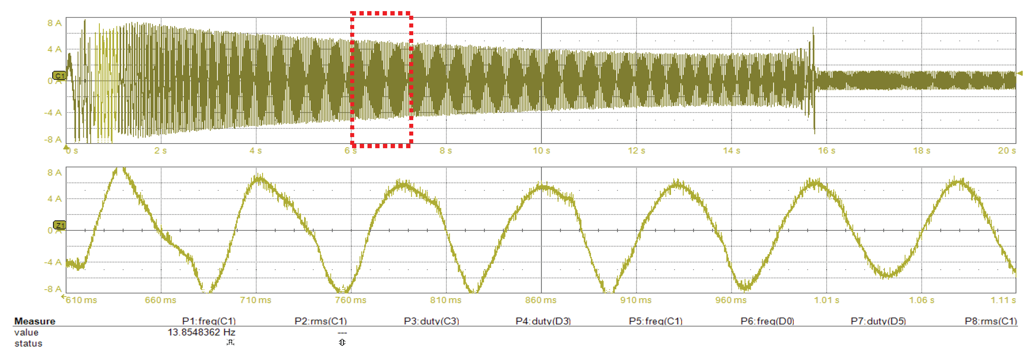
Figure 18.
Standstill to 82 rpm without any voltage drop compensation (motor fails to start-up), top) Inverter phase current during start-up, bottom) zoom in around 16s (0.186 s / div).
Figure 18.
Standstill to 82 rpm without any voltage drop compensation (motor fails to start-up), top) Inverter phase current during start-up, bottom) zoom in around 16s (0.186 s / div).
6.2. Deceleration to Low-Speed Validation
In this section, we explore a scenario where the motor decelerates to a speed of 82 rpm. Figure 21 and Figure 22 depict the motor current behavior as it decelerates from 400 rpm to 82 rpm, utilizing our proposed voltage drop compensation methodology. It is evident from these figures that the motor effectively achieves and maintains the desired lower speed as commanded.
A similar scenario is depicted in Figure 23, where results from GUI illustrate the d and q component of motor current along with other crucial controller parameters. In this scenario the motor runs at 1,000 rpm and then is commanded to decelerate down to 82 rpm under maximum loading.
6.3. High Speed Validation
In this section the proposed enhanced FOC scheme is tested over the entire motor speed range. Beyond 6,000 rpm the VSI reaches its nominal voltage and flux weakening is engaged. Also, beyond 2,000 rpm, as described in Section 4.3, the impact of voltage drop becomes less significant, and the controller deactivates the proposed methodology, transitioning to a conventional FOC scheme.
Figure 24 illustrates the motor dq current components along with the reference motor speed in rpm, the flux observer estimated speed in rad/s, and the DC-link voltage. The results showcase the scenario where the motor accelerates from 400 rpm to 6,000 rpm. Figure 25 showcases the scenario where the motor accelerates from 7,100 to 9,000 rpm. The engagement of flux-weakening is evident from the growth in the d-component of the motor current. Finally, Figure 26 and Figure 27 show the actual motor current while the motor operates at 8,500 and 9,000 rpm, respectively.
The results presented signify effective motor controllability over the entire motor speed range, including the engagement of flux-weakening and the disengage of proposed methodology.
7. Conclusions
In this work, an enhanced FOC scheme that accounts for the inverter voltage drop is proposed, enabling the efficient drive of brushless machines at very low motor-speeds. About the controllability of the motor, it has been shown that the inverter voltage drops play a significant role in low-end microcontrollers. It has also been shown that the controller performance is severely affected by the inverter voltage drop and the low control bandwidth of conventional MCUs, driving the motor unreliably at the low-speed range. Based on the presented results, the proposed methodology mitigates this problem because it accounts for the voltage drops within the FOC control scheme. At higher speeds where the impact of the voltage-drops is less significant the proposed methodology deactivates and the controller transitions to a conventional FOC controller. Experimental results have been presented verifying the very good performance of the controller up to 9,000 rpm and down to 82 rpm. As the next step the effectiveness of such method will be verified by applying it to a real application use case, to consider for example the drum dynamic of a washing machine.
Author Contributions
Conceptualization, D.V. and M.P.; methodology, D.V.; software, D.V and M.P; validation, D.V., and M.P.; writing—original draft preparation, D.V.; writing—review and editing, D.V, N.P.; and M.P. All authors have read and agreed to the published version of the manuscript.
Funding
This research received no external funding.
Data Availability Statement
Not applicable.
Acknowledgments
We would like to express our gratitude to the Department of Solution Engineering Center of onsemi in Munich and particularly Martin Embacher for their invaluable assistance in conducting this work, as well as for their generous provision of the hardware, including the SECO-1KW-MCTRL-GEVB evaluation board, motor-generator system, and essential laboratory equipment for carrying out the experimental part of this work.
Conflicts of Interest
The authors declare no conflict of interest.
References
- Leonhard, W. Control of Electrical Drives. Berlin, Germany: Springer-Verlag, 1996.
- Santisteban, J.A.; Stephan, R.M. Vector control methods for induction machines: an overview. IEEE Trans. Educ. 2001, 44, 170–175. [CrossRef]
- M. Ahmad, “High Performance AC Drives: Modelling Analysis and Control,” published by Springer-Verlag, 2010.
- AlShanfari, A.K.; Wang, J. Influence of control bandwidth on stability of permanent magnet brushless motor drive for ‘more electric’ aircraft systems. Proc. Int. Conf. Elect. Mach. Syst. (ICEMS) 2011, 1–7.
- www.infineon.com. Available online: https://www.infineon.com/cms/en/product/microcontroller/32-bit-industrial-microcontroller-based-on-arm-cortex-m/32-bit-xmc1000-industrial-microcontroller-arm-cortex-m0/xmc1400/ (05 January 2024).
- www.infineon.com. Available online: https://www.infineon.com/cms/en/product/microcontroller/32-bit-psoc-arm-cortex-microcontroller/psoc-4-32-bit-arm-cortex-m0-mcu/?term=PSoC4&view=kwr&intc=searchkwr (05 January 2024).
- https://www.st.com. Available online: https://www.st.com/content/st_com/en/search.html#q=STM32G0-t=products-page=1 (05 January 2024).
- www.ti.com. Available online: https://www.ti.com/microcontrollers-mcus-processors/arm-based-microcontrollers/products.html (05 January 2024).
- www.nxp.com. Available online: https://www.nxp.com/products/processors-and-microcontrollers/arm-microcontrollers/general-purpose-mcus/lpc800-arm-cortex-m0-plus-:MC_71785 (05 January 2024).
- A. Anuchin, M. Gulyaeva, and F. Briz “Modeling of AC voltage source inverter with dead-time and voltage drop compensation for DPWM with switching loss minimization,” in Proc. the 7 th International Conference on Modern Power Systems 2017, Jul. 2017.
- D. C. Pham, “Modeling and simulation of two level three-phase voltage source inverter with voltage drop,” Seventh Int. Conf. on Information Science and Technology, pp. 317–322, 2017.
- Y. Nakamura, H. Funato, and S. Ogasawara, “Compensation of output voltage distortion analysis of pwm inverter with lc filter caused by device voltage drop,” in Power Electronics and Applications, 2007 European Conference on, pp. 1–9, IEEE, 2007.
- Choi, J.-W.; Sul, S.-K. Inverter output voltage synthesis using novel dead time compensation. IEEE Trans. Power Electron. 1996, 11, 221–227. [CrossRef]
- Leggate, D.; Kerkman, R.J. Pulse-based dead-time compensator for PWM voltage inverters. IEEE Trans. Ind. Electron. 1997, 44, 191–197. [CrossRef]
- Zhang, Z.; Xu, L. Dead-Time Compensation of Inverters Considering Snubber and Parasitic Capacitance. IEEE Trans. Power Electr. 2014, 29, 3179–3187. [CrossRef]
- Urasaki, N.; Senjyu, T.; Uezato, K.; Funabashi, T. An adaptive deadtime compensation strategy for voltage source inverter fed motor drives. IEEE Trans. Power Electron. 2005, 20, 1150–1160. [CrossRef]
- Cichowski, A.; Nieznanski, J. Self-tuning dead-time compensation method for voltage-source inverters. IEEE Power Electron. Lett. 2005, 3, 72–75. [CrossRef]
- G. Zhao S. Nalakath Y. Sun J. Wiseman and A. Emadi "Inverter voltage drop characterisation considering junction temperature effects" Proc. IEEE Transp. Electrific. Conf. Expo. pp. 1-6 Jun. 2019.
- R. Bojoi E. Armando G. Pellegrino and S. G. Rosu "Self-commissioning of inverter nonlinear effects in AC drives" Proc. IEEE Energy Conf. Exhib pp. 213-218 Sep. 9–12 2012.
- Shang, C.; Yang, M.; Long, J.; Xu, D.; Zhang, J.; Zhang, J. An accurate VSI nonlinearity modeling and compensation method accounting for DC-link voltage variation based on LUT. IEEE Trans. Ind. Electron. 2022, 69, 8645–8655. [CrossRef]
- Pellegrino, G.; Bojoi, I.R.; Guglielmi, P.; Cupertino, F. Accurate inverter error compensation and related self-commissioning scheme in sensorless induction motor drives. IEEE Trans. Ind. Appl. 2010, 46, 1970–1978. [CrossRef]
- Tuovinen, T.; Hinkkanen, M. Comparison of a reduced-order observer and a full-order observer for sensorless synchronous motor drives. IEEE Trans. Ind. Appl. 2012, 48, 1959–196. [CrossRef]
- K. Bose, “Modern Power Electronics and AC Drives,” Prentice Hall, Upper Saddle River, 2002.
- Miguel-Espinar, C.; Heredero-Peris, D.; Villafafila-Robles, R.; Montesinos-Miracle, D. Review of Flux-Weakening Algorithms to Extend the Speed Range in Electric Vehicle Applications With Permanent Magnet Synchronous Machines. IEEE Access 2023, 11, 22961–22981. [CrossRef]
- Maksimović, Dragan and Robert W. Erickson. “Advances in Averaged Switch Modeling and Simulation.” (1999).
- https://www.onsemi.com. Available online https://www.onsemi.com/solutions/technology/motor-development-kit-mdk (15 February 2024).
- https://www.onsemi.com. Available online: https://www.onsemi.com/pub/Collateral/AND9390-D.PDF (15 February 2024).
Figure 1.
Electrical diagram of system under study.
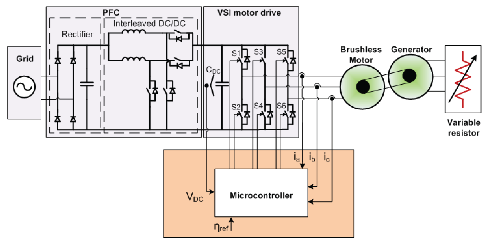
Figure 2.
Typical FOC block diagram.
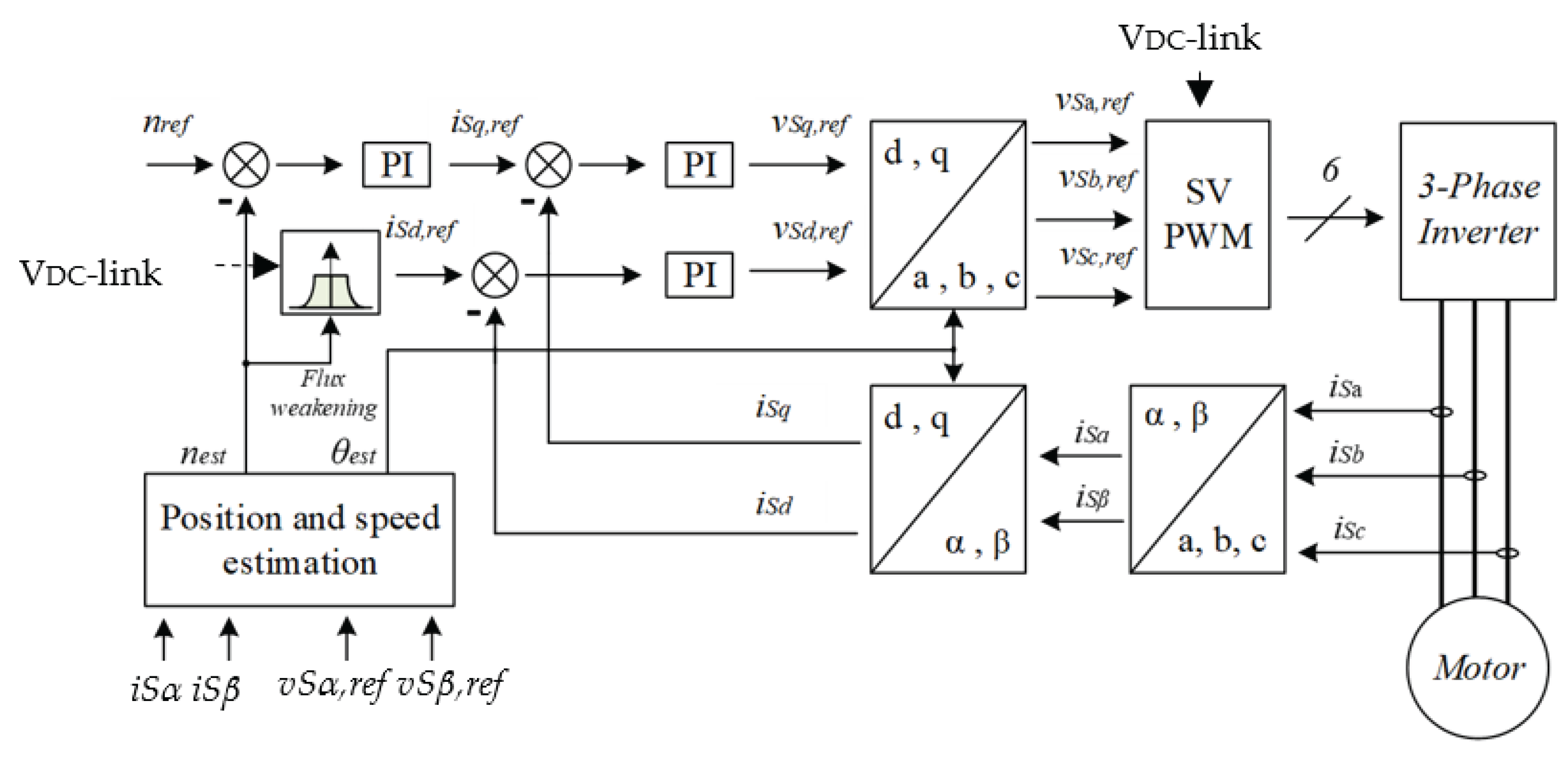
Figure 3.
Voltage quantities represented in a leg of the 3-phase B6 Inverter.
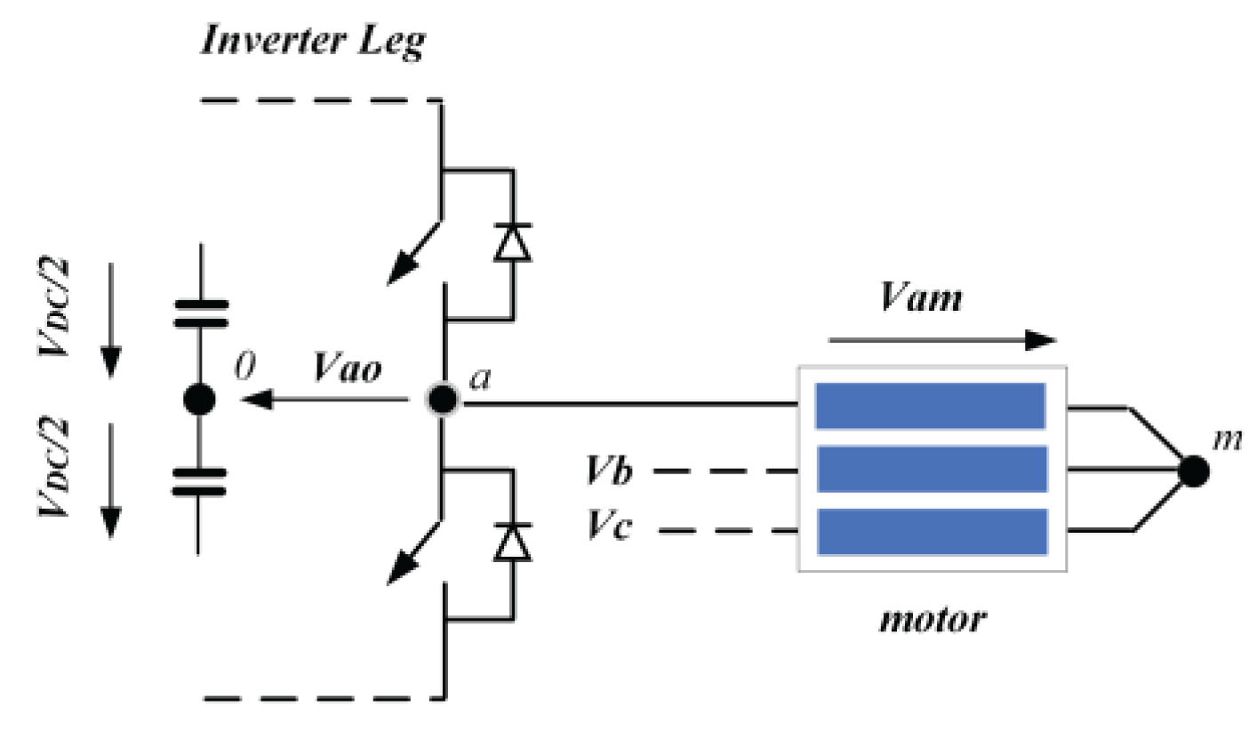
Figure 4.
Impact of the asymmetrical dead-time on vxo (case of negative current).
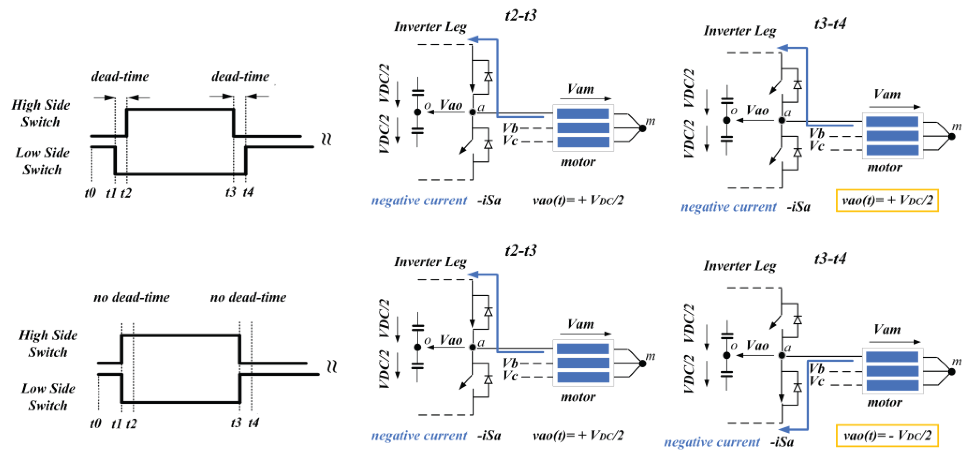
Figure 5.
Impact of the asymmetrical dead-time on vxo (case of positive current).
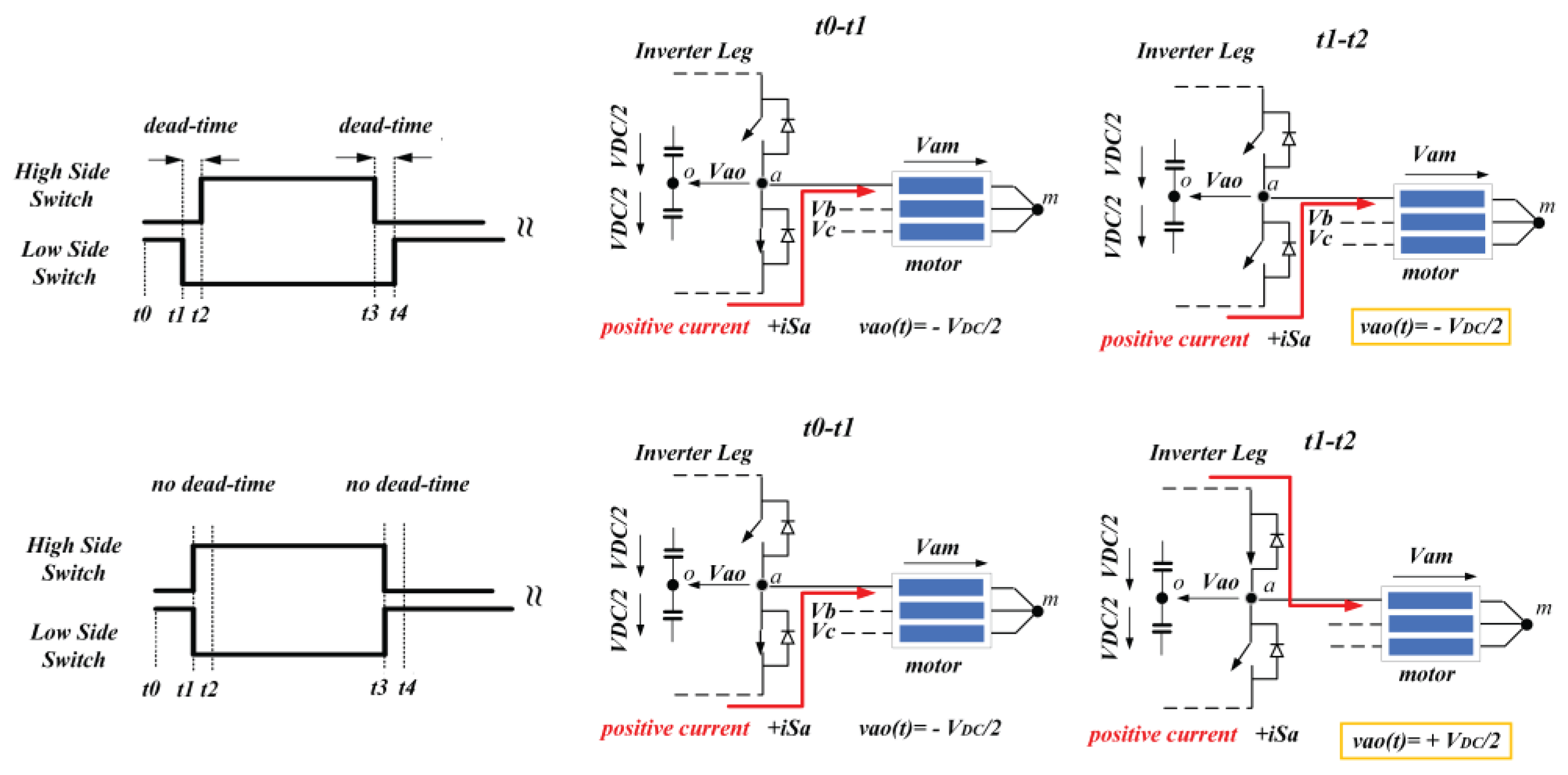
Figure 6.
Sinusoidal current waveform (top), voltage drop of phase a motor winding vam,drop(t)* (middle) inverter output vao,drop(t)* (bottom).
Figure 6.
Sinusoidal current waveform (top), voltage drop of phase a motor winding vam,drop(t)* (middle) inverter output vao,drop(t)* (bottom).
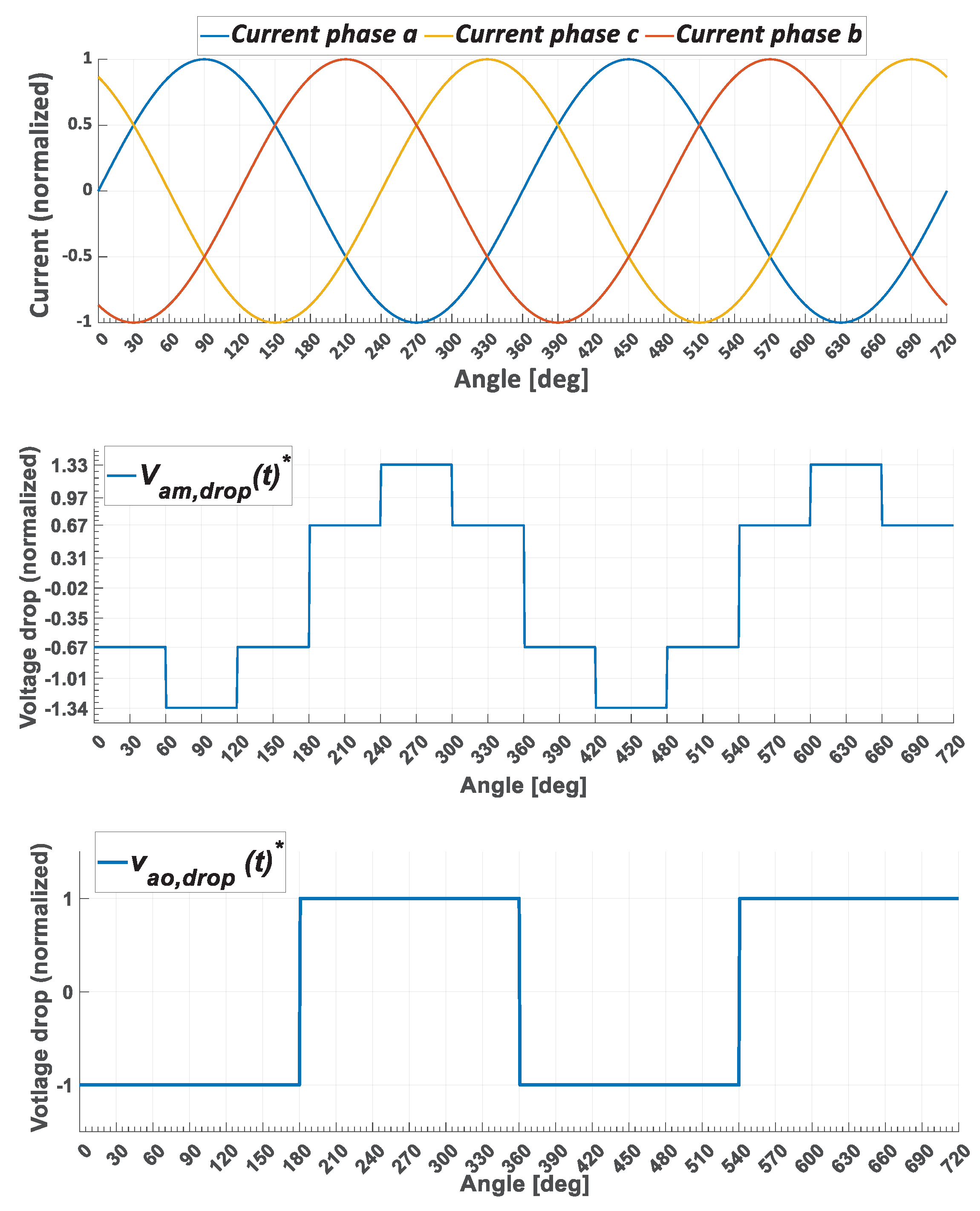
Figure 7.
αβ0 and dq0 component of inverter and winding motor voltage.
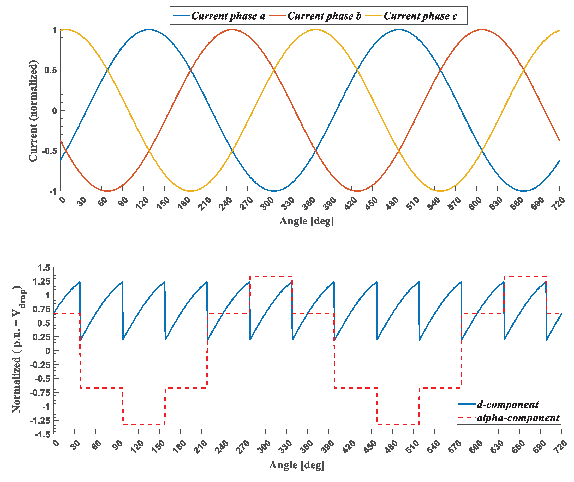
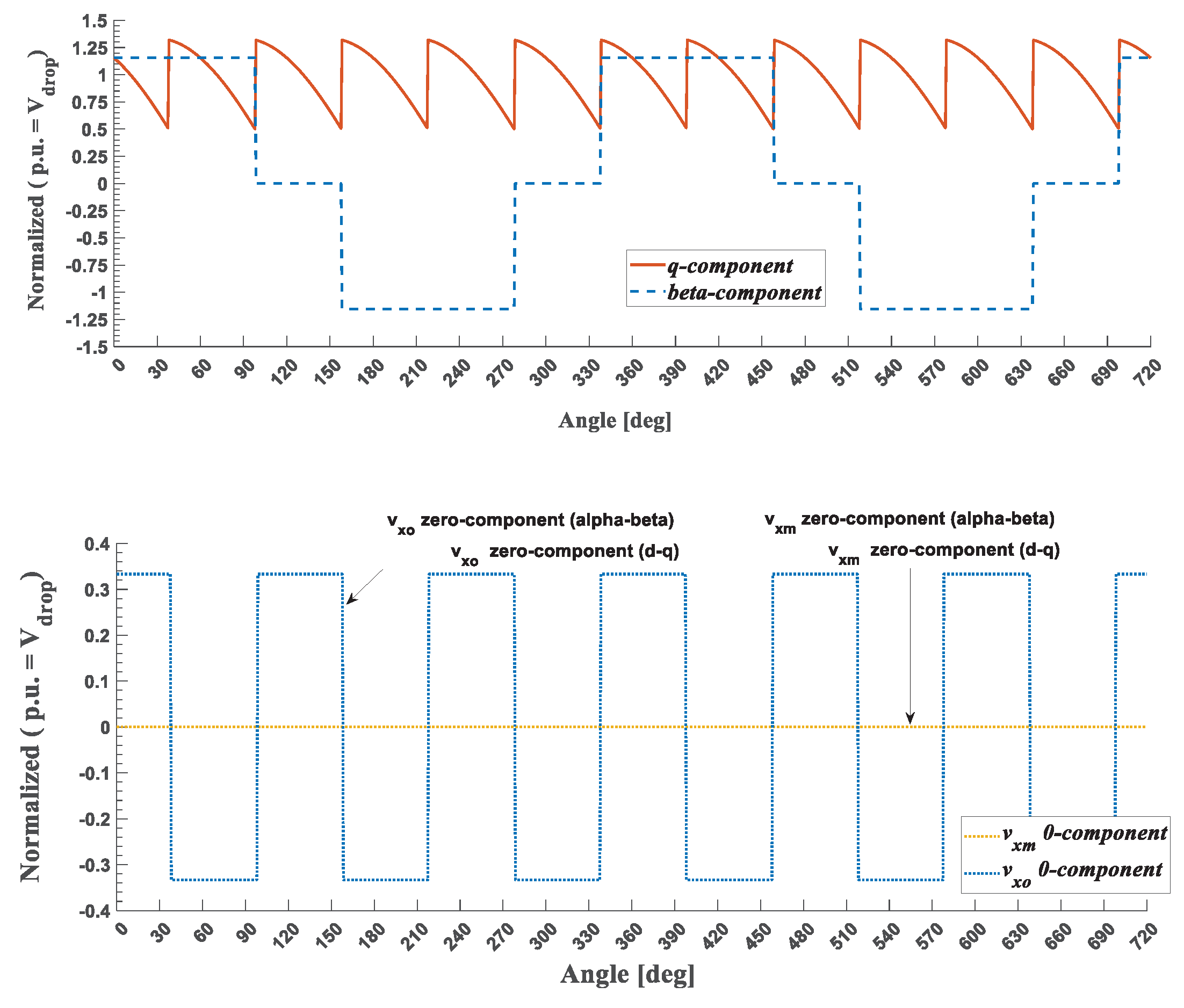
Figure 8.
Proposed methodology for the incorporation of inverter voltage drops in FOC αβ-reference frame.
Figure 8.
Proposed methodology for the incorporation of inverter voltage drops in FOC αβ-reference frame.
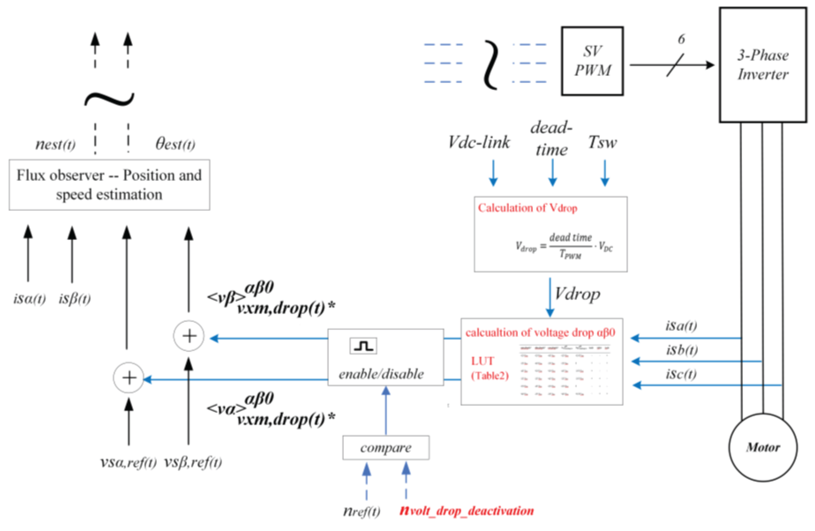
Figure 10.
System outputs (x-axis 5sec/div) with direct compensation at abc- reference frame for dead time (us) a) 0.5, b) 1.5, c) 1.9, d) 2,0.
Figure 10.
System outputs (x-axis 5sec/div) with direct compensation at abc- reference frame for dead time (us) a) 0.5, b) 1.5, c) 1.9, d) 2,0.
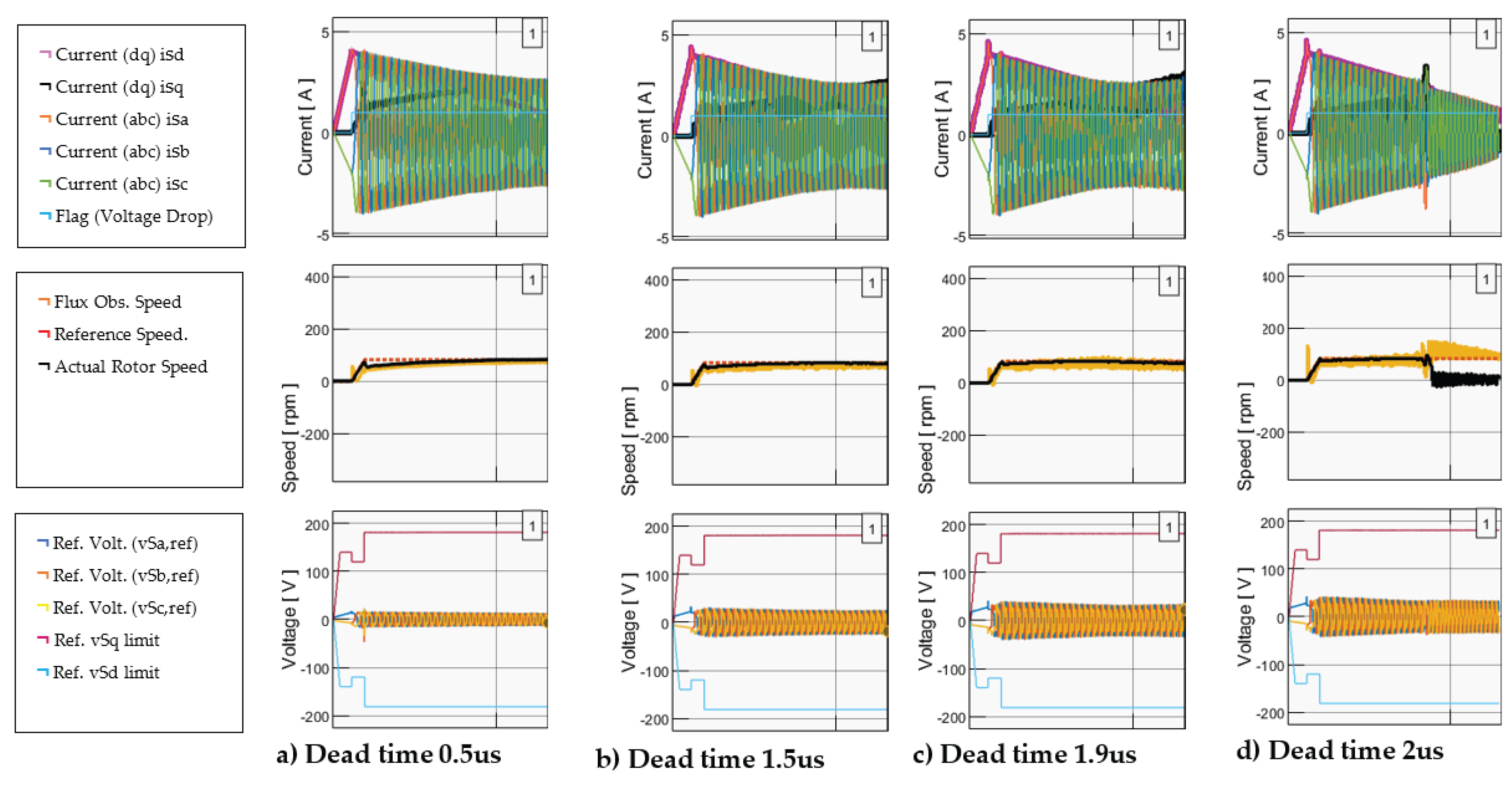
Figure 11.
System response (5sec/div) with proposed compensation at αβ-reference frame for dead time (us) a) 0.5, b) 1.5, c) 1.9, d) 2,0.
Figure 11.
System response (5sec/div) with proposed compensation at αβ-reference frame for dead time (us) a) 0.5, b) 1.5, c) 1.9, d) 2,0.
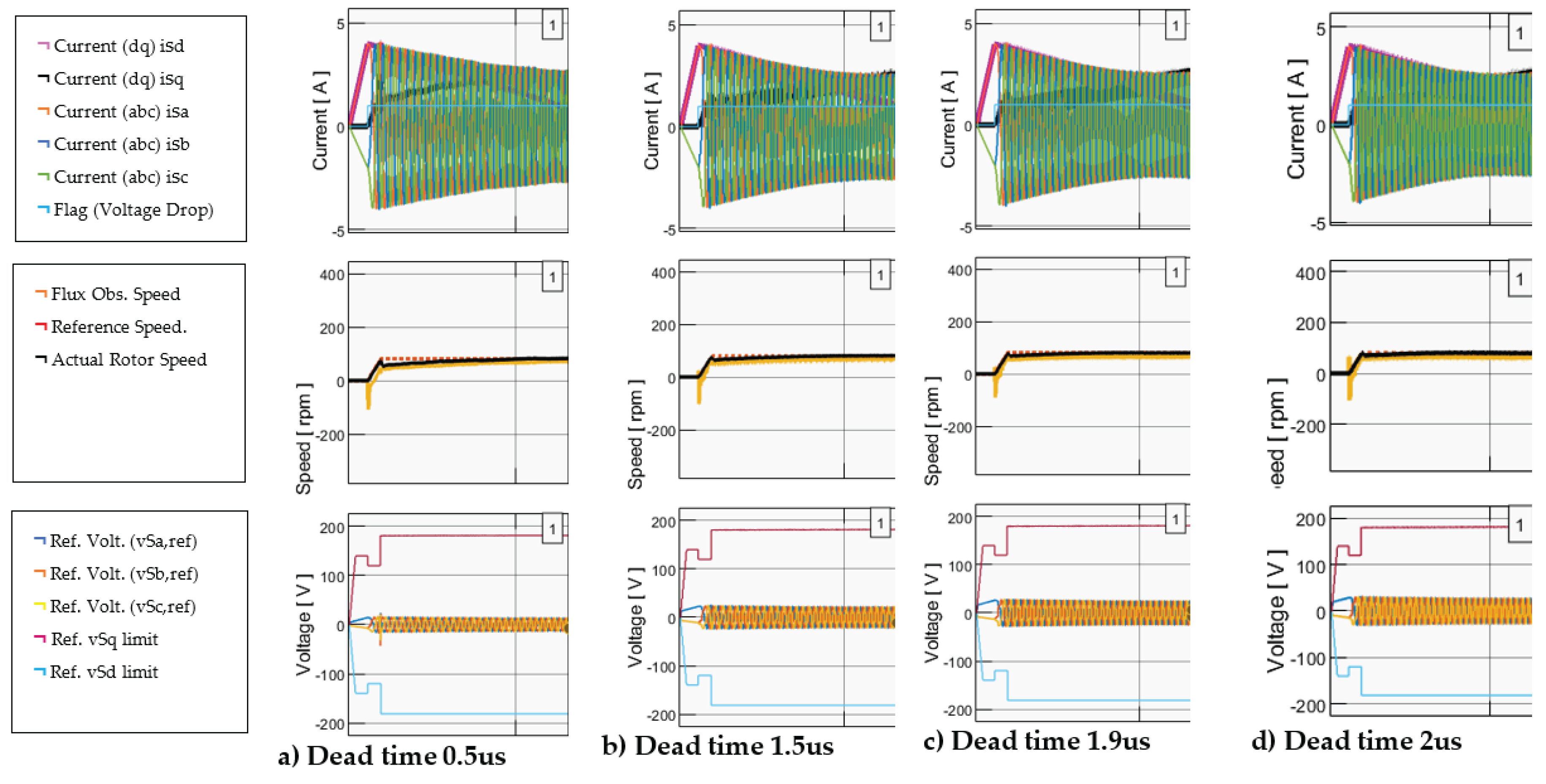
Figure 12.
System response (5sec/div) for 2,0 us dead time a) without compensation b) with direct compensation at abc-reference frame, c) with the proposed compensation at αβ-reference frame.
Figure 12.
System response (5sec/div) for 2,0 us dead time a) without compensation b) with direct compensation at abc-reference frame, c) with the proposed compensation at αβ-reference frame.
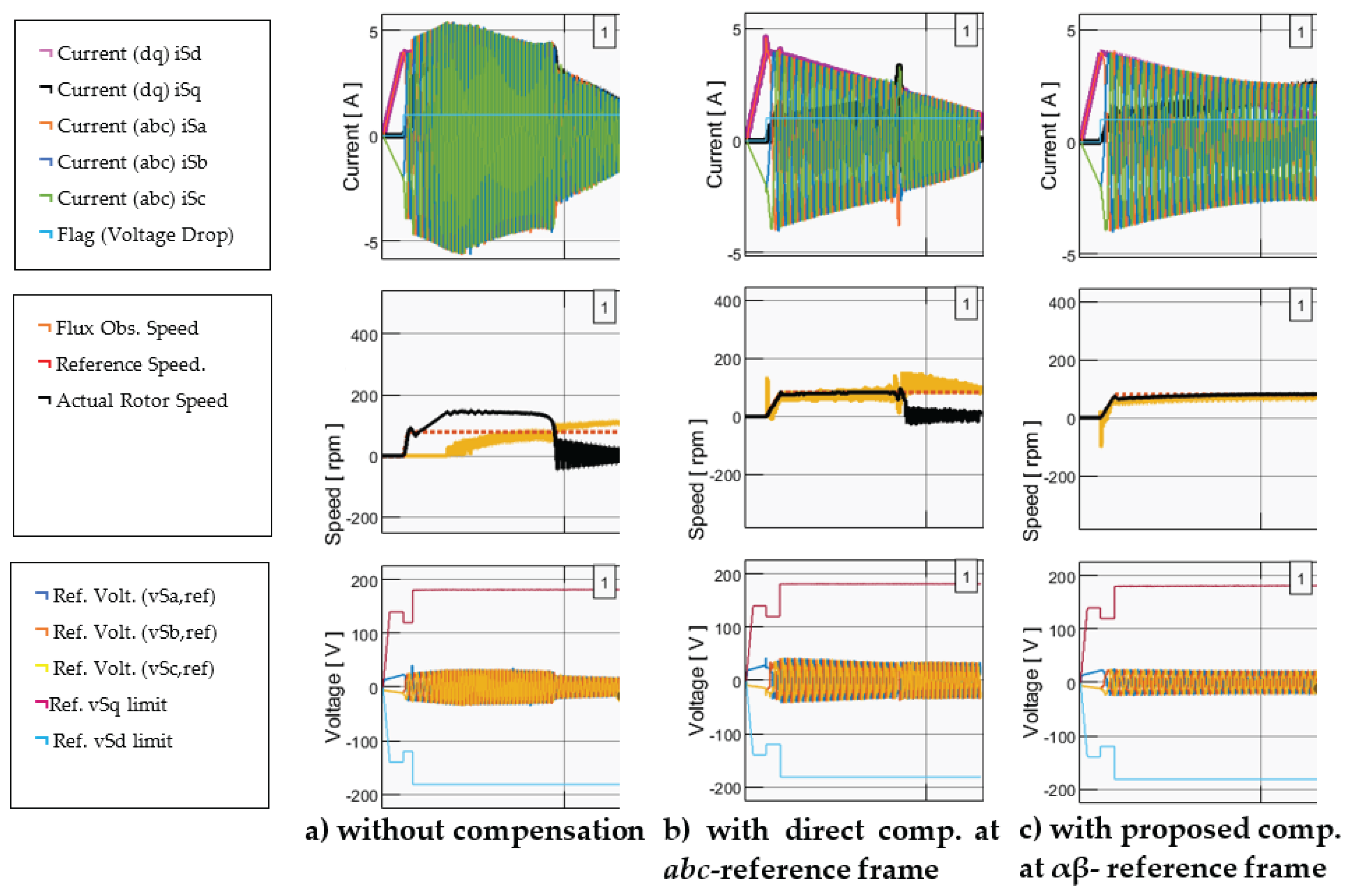
Figure 13.
System response when the motor is commanded from stall to maximum speed (7,000 rpm) and back to 82 rpm.
Figure 13.
System response when the motor is commanded from stall to maximum speed (7,000 rpm) and back to 82 rpm.
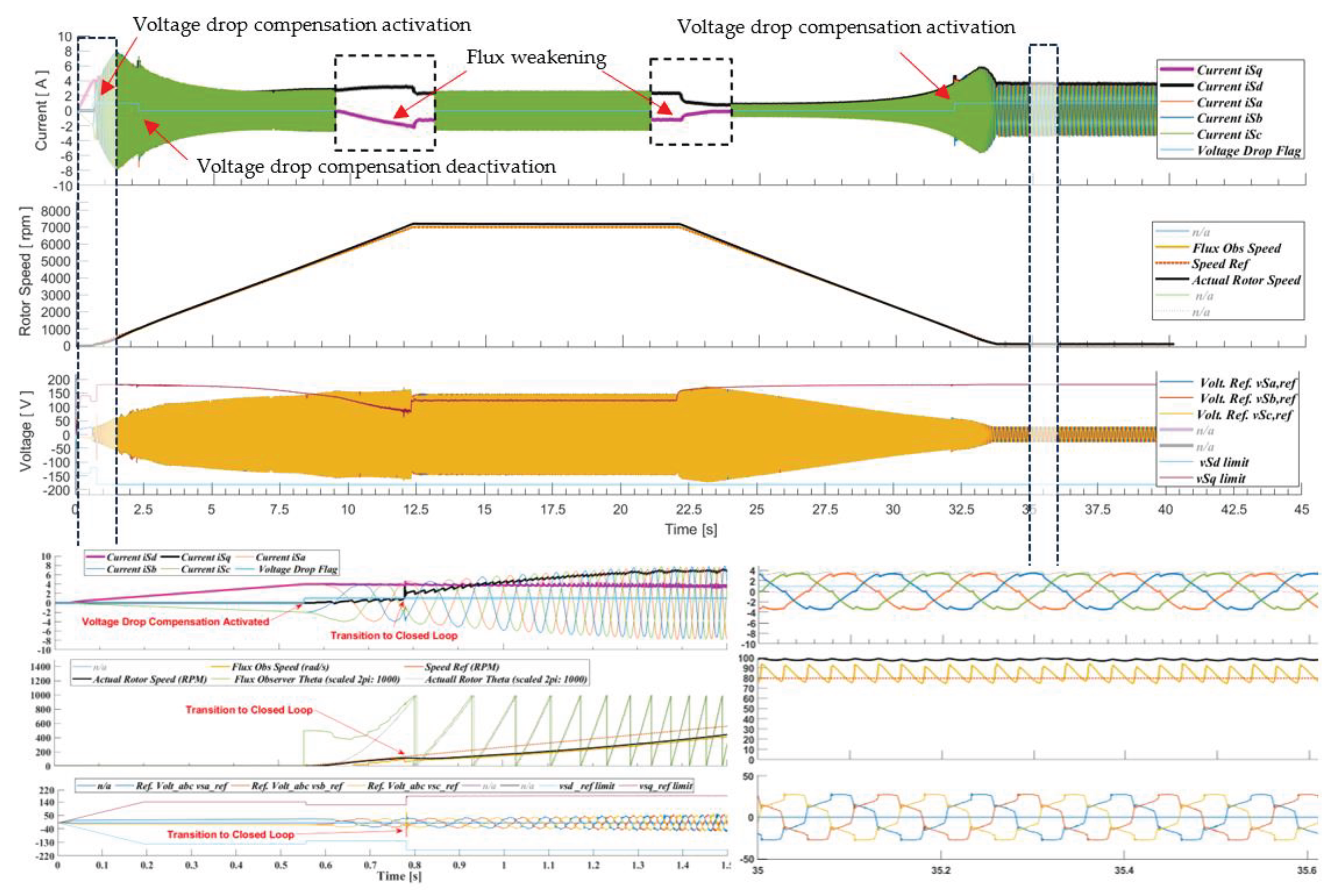
Figure 14.
Overview of the experimental set-up.
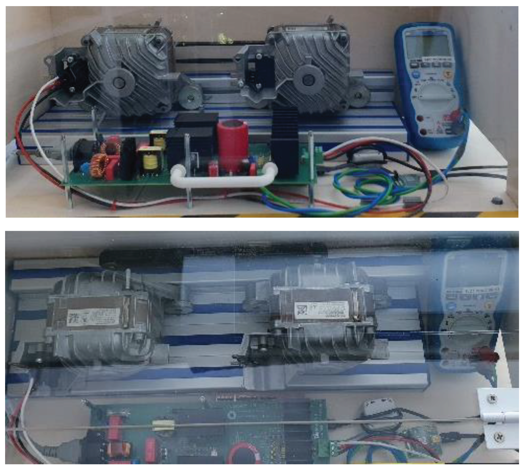
Figure 15.
SECO-1KW-MCTRL-GEVB evaluation board [26].
Figure 15.
SECO-1KW-MCTRL-GEVB evaluation board [26].
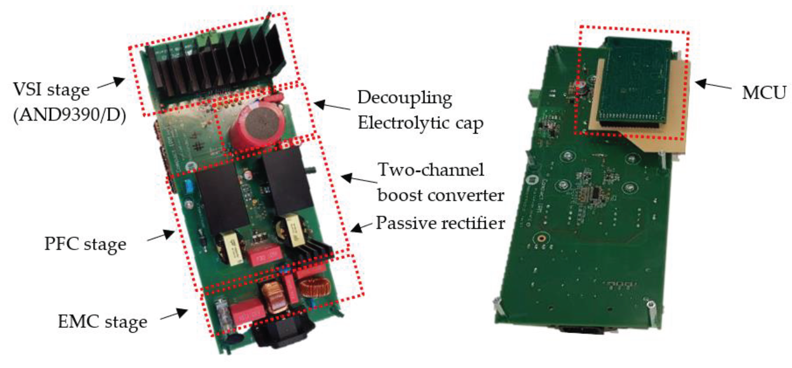
Figure 21.
With the proposed method at very low motor speeds; Inverter phase current during the transition of the motor from 400 rpm to 82 rpm (1 s / div).
Figure 21.
With the proposed method at very low motor speeds; Inverter phase current during the transition of the motor from 400 rpm to 82 rpm (1 s / div).
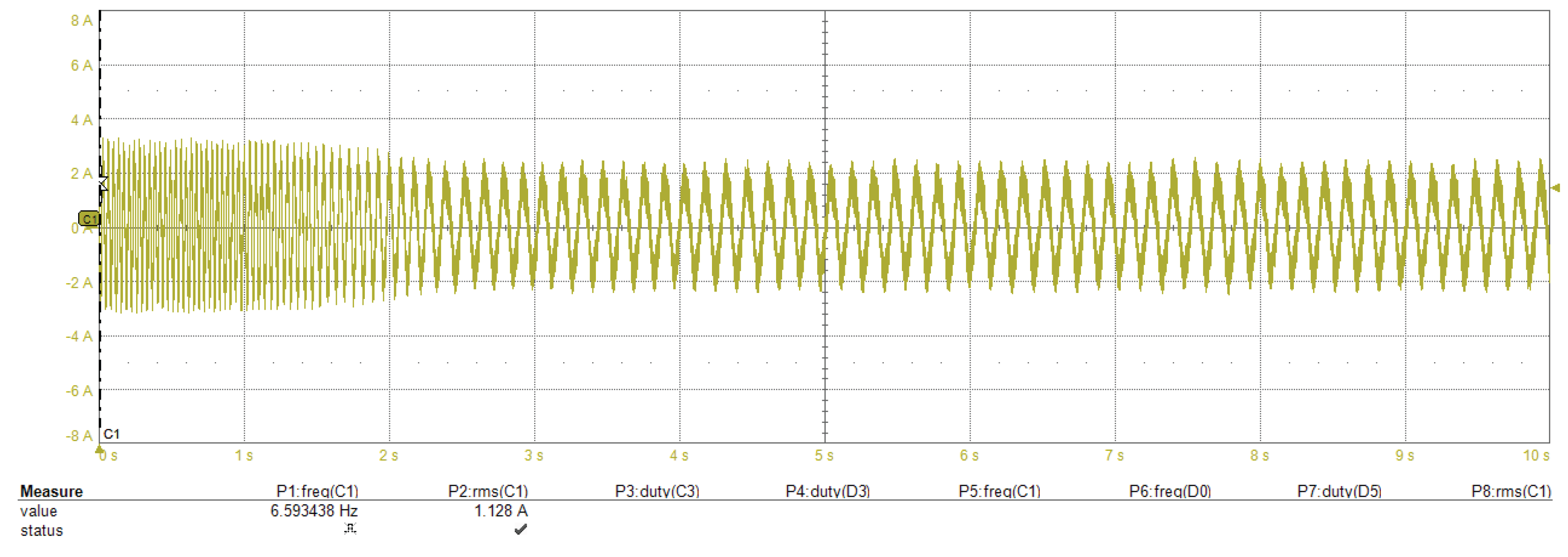
Figure 22.
With the proposed method at very low motor speeds; Zoom in steady-state inverter phase current waveform at 82 rpm (0.2 s / div).
Figure 22.
With the proposed method at very low motor speeds; Zoom in steady-state inverter phase current waveform at 82 rpm (0.2 s / div).
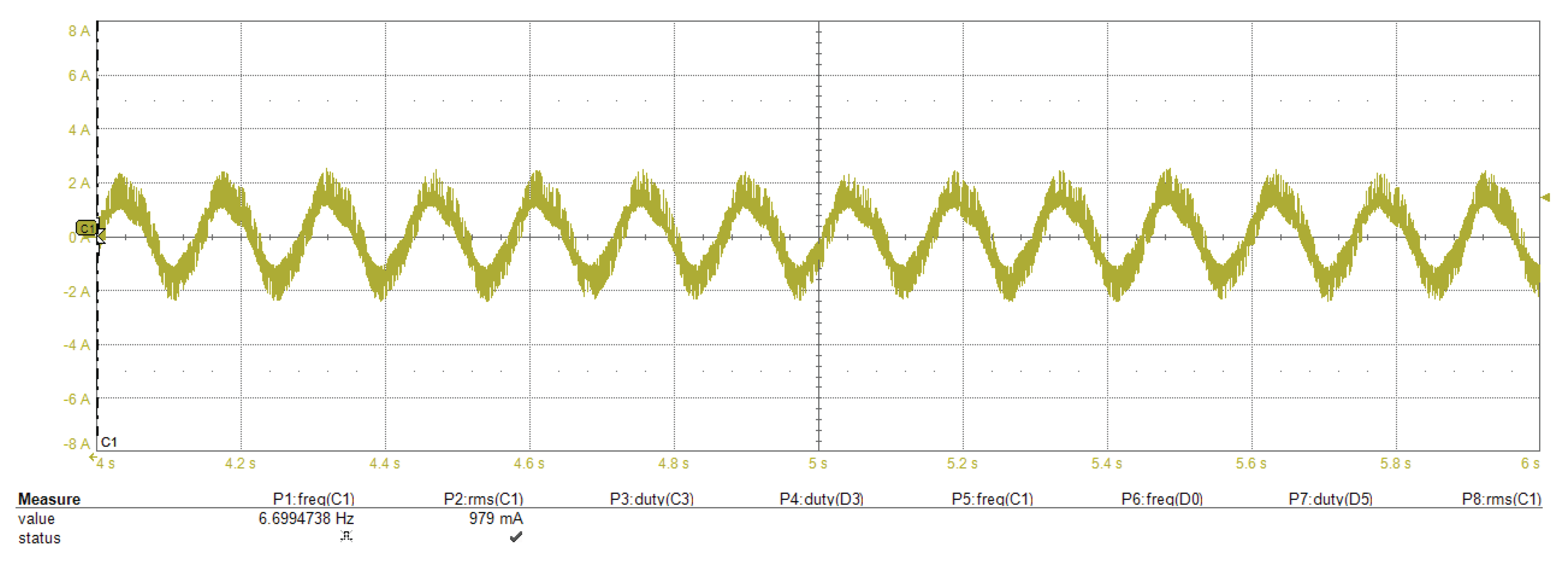
Figure 23.
GUI interface captures during the motor deceleration from 1,000 rpm to 82 rpm with proposed method.
Figure 23.
GUI interface captures during the motor deceleration from 1,000 rpm to 82 rpm with proposed method.
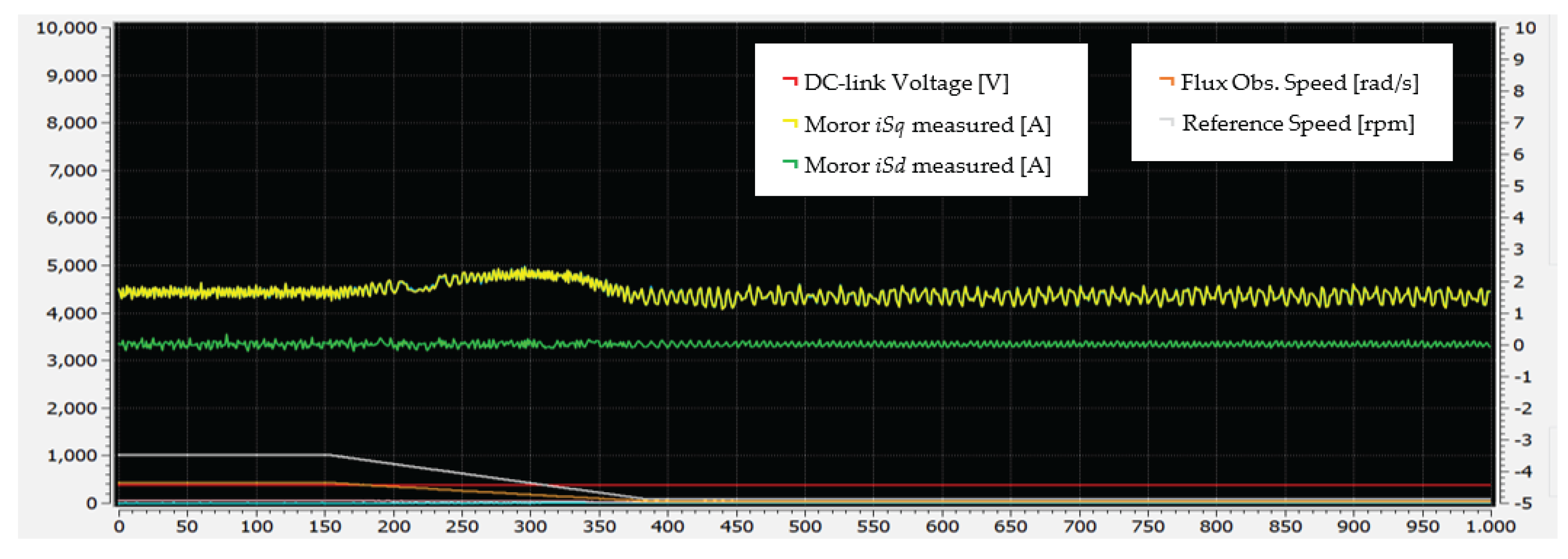
Figure 24.
GUI interface captures during motor acceleration from 400 rpm to 6,000 rpm.
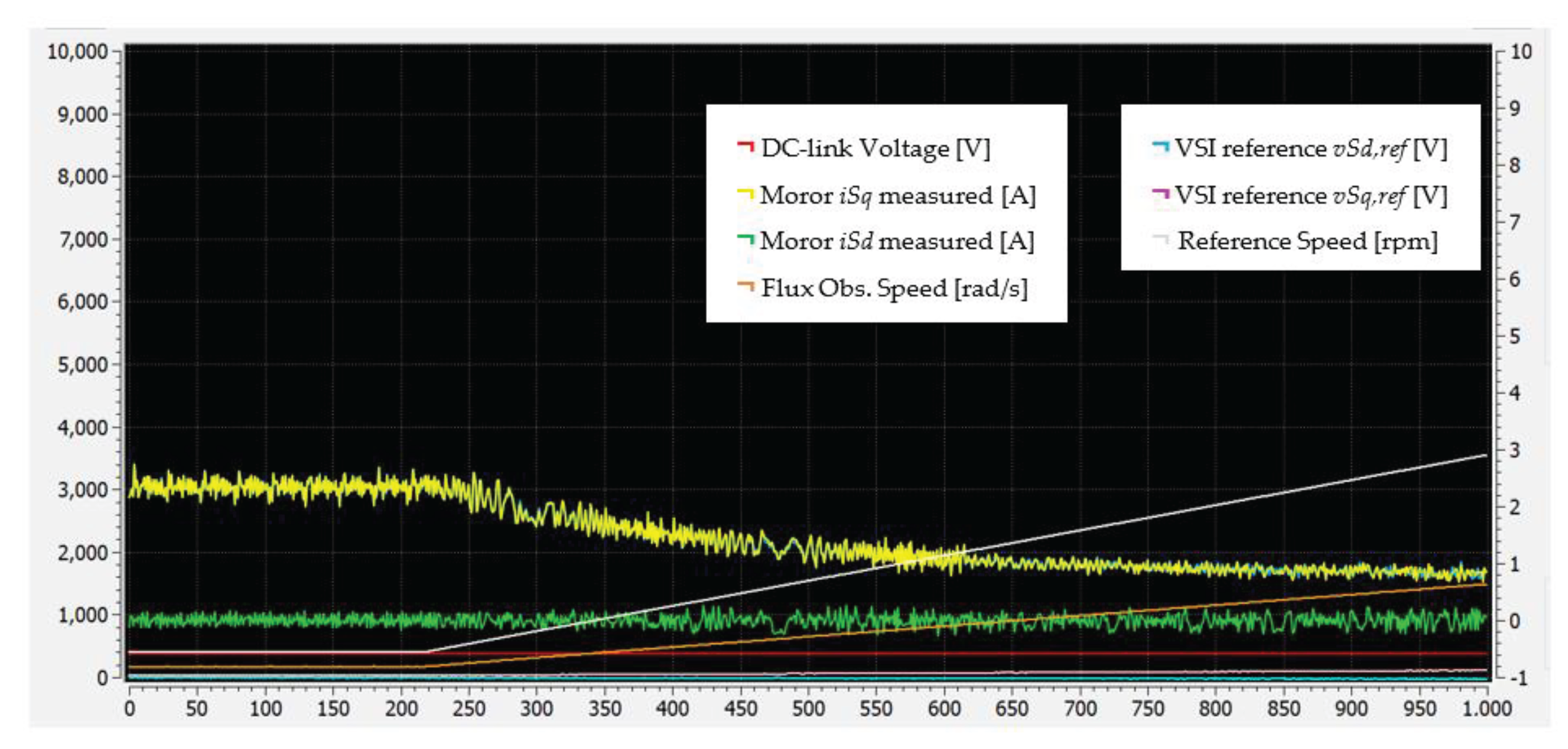
Figure 25.
GUI interface captures during motor acceleration from 7,100 rpm to 9,000 rpm.
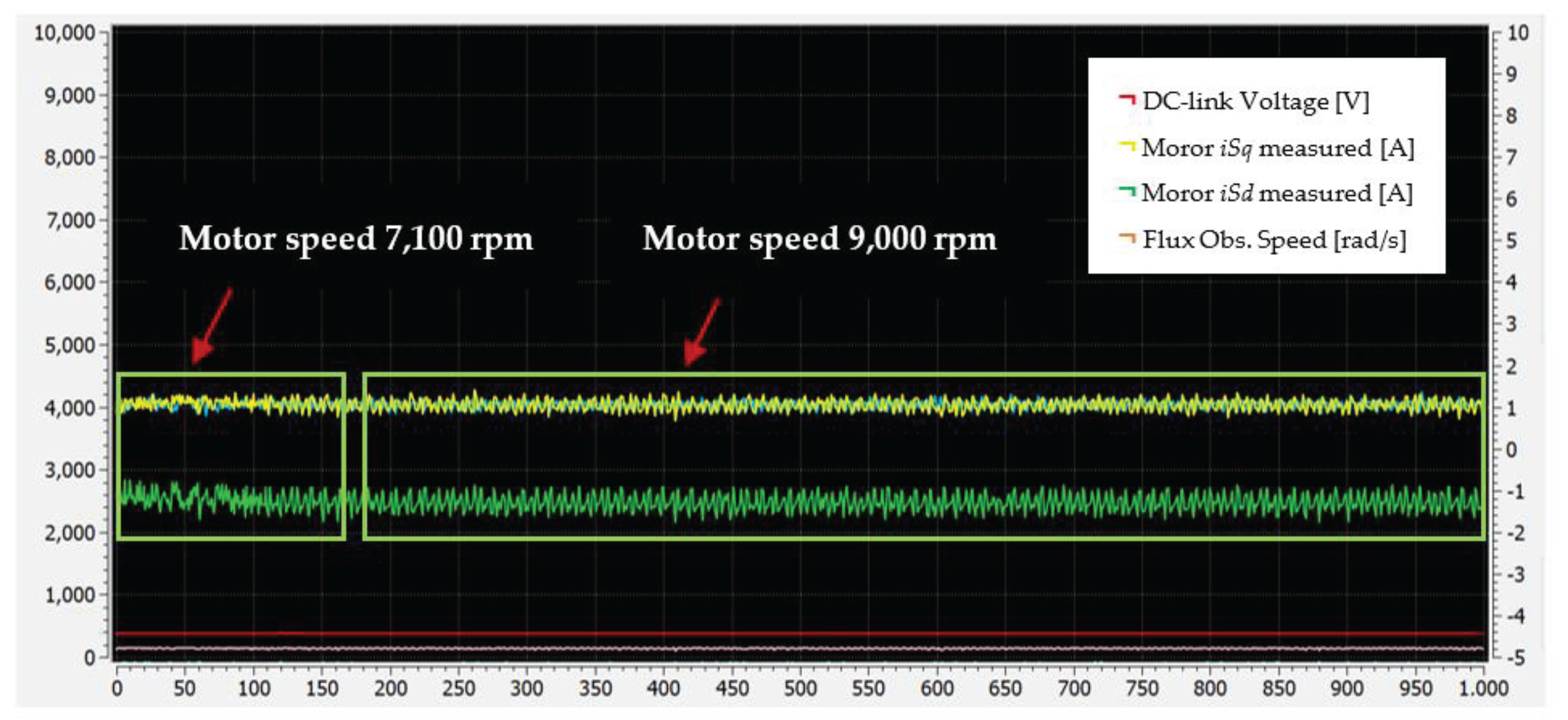
Figure 26.
Steady-state inverter phase current waveform at 8,500 rpm.
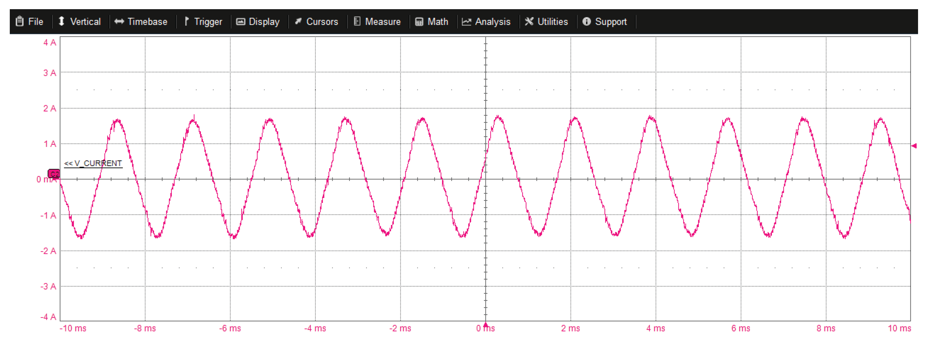
Figure 27.
Steady-state inverter phase current waveform at 9,000 rpm.
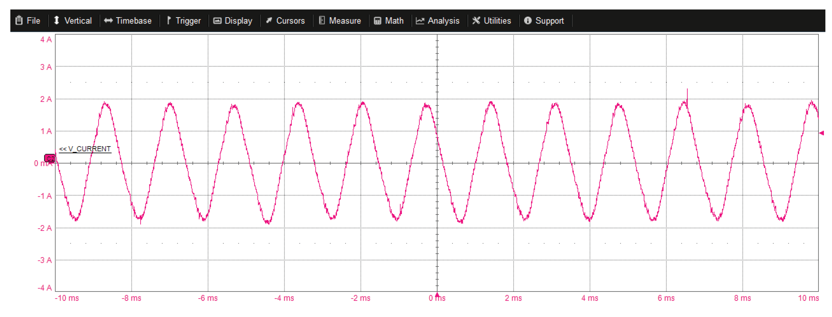
Table 1.
Recap of vam,drop(t)* vao,drop(t)*.
| vam,drop(t)* | vao,drop(t)* | isa | isb | isc |
|---|---|---|---|---|
| -2/3 Vdrop | -1 Vdrop | + | - | + |
| -4/3 Vdrop | -1 Vdrop | + | - | - |
| -2/3 Vdrop | -1 Vdrop | + | + | - |
| +2/3 Vdrop | +1 Vdrop | - | + | - |
| +4/3 Vdrop | +1 Vdrop | - | + | + |
| +2/3 Vdrop | +1 Vdrop | - | - | + |
Table 4.
Experimental test bench system parameters.
| SECO-1KW-MCTRL-GEVB | Value | Bosch Motor | Value |
|---|---|---|---|
| PFC output voltage (V) | 380 | Motor nominal power (W) | 545 |
| VSI Switch. Frequency (kHz) | 16 | Motor nominal speed (rpm) | 6,000 |
| Dead-time (us) | 2 (asymm.) | Motor maximum speed (rpm) | 9,500 |
| System efficiency PFC+VSI | 96%??? | Motor winding inductance (mH) | 16 |
| Modulation | SV-PWM | Motor winding resistance (Ω) | 2.5 |
| MCU PWM resolution (bits) | 10.29 | Motor Pole Pairs | 4 |
| 3Actual MCU ADC interval | 6 us | BEMF constant (voltage2/rpm) | 0.028138 |
| Proposed methodology deactivation speed (rpm) | 2,000 |
2Peak phase voltage 3Total conversion and data transfer interval of measuring 3.0 currents and 1.0 bus voltage.
Disclaimer/Publisher’s Note: The statements, opinions and data contained in all publications are solely those of the individual author(s) and contributor(s) and not of MDPI and/or the editor(s). MDPI and/or the editor(s) disclaim responsibility for any injury to people or property resulting from any ideas, methods, instructions or products referred to in the content. |
© 2024 by the authors. Licensee MDPI, Basel, Switzerland. This article is an open access article distributed under the terms and conditions of the Creative Commons Attribution (CC BY) license (http://creativecommons.org/licenses/by/4.0/).
Copyright: This open access article is published under a Creative Commons CC BY 4.0 license, which permit the free download, distribution, and reuse, provided that the author and preprint are cited in any reuse.


