
Submitted:
21 February 2024
Posted:
22 February 2024
You are already at the latest version
Abstract
Scaling up the production of power devices involves, in the semiconductor industry, the use of large semiconductor 8” and 12” wafers of Si or SiC. Their use implicates a successful an effective monitoring and control of wafer warpage, as the geometrical size of the substrate increases, as well as a command control on the degeneration of non-linear warpage into critical phenomena known as bifurcation or buckling.To mitigate the warpage, the use of taiko wafers, which consists of wafers having a thicker region on the rim region of the wafer, has been generally adopted in the production lines. In a previous work [1] we investigated the warpage of taiko wafers by introducing the concept of equivalent thickness, in the linear approximation, for the case of a front side metalized taiko wafer. However, as the thickness of the central semiconductor substrate region decreases the possibility that also the taiko wafer bifurcates emerges. For this reason, in this work we have investigated the occurrence of bifurcation or buckling in a taiko wafer. In particular, we implemented a finite element analysis method by using ANSYS Mechanical Enterprise 2023/R2 to investigate the phenomenon of bifurcation in a taiko wafer. The investigated system consisted of a 200 mm Si (001) front side metalized (FSM) taiko wafer, having a substrate thickness ranging from 100 µm to 400 µm, with a step height fixed to 450 µm. The FSM layer consisted of an Al layer of 4.5 µm thin. The system was subjected to a thermal load such that, getting cooled from a nominal temperature T to 25°C, the metal layer can develop a residual stress. To investigate the bifurcation, an asymmetry was induced in the system by applying a slight force on a point of the circumferential region perpendicularly to the substrate. The temperature investigated ranged from 30 °C to 170 °C. From this investigation, it results that also the bifurcation is mitigated by the taiko structure. Indeed, the bifurcation emerges at higher values of the stresses with respect to the case of flat wafers having the same size and thickness of the substrate. Moreover, the concept of equivalent thickness needs to be reformulated by taking into account of the bifurcation phenomenon. Indeed, from the warpage at the bifurcation point of the taiko wafer, we can determine an overall equivalent thickness of the taiko wafer.
Keywords:
Bifurcation
; Taiko wafers
; Finite Element Analysis (FEA)
; ANSYS
; Thermomechanical Simulations
; Warpage
; Modelling
; Equivalent Thickness
Introduction
A scale-up of the semiconductor integration process of power devices, involving the use of large (e.g. 8" and 12") Si or SiC wafers, requires an accurate control of the wafer warpage since early stages of the large-scale integration process, to prevent undesirable asymmetric degeneration of the warpage, known as wafer bifurcation or buckling. A commonly adopted solution is the taiko method [1], which involves creating a thicker ring region around the wafer’s rim to mitigate this issue. In previous research [2,3] we delved into the factors influencing the warpage of a front side metalized (FSM) taiko wafer in the linear case and introduced the concept of equivalent thickness of a taiko wafer. In this work, we investigated the behaviour of a taiko wafer with respect to the bifurcation. The main question regards the extension of the concept of equivalent thickness in the non-linear range where bifurcation phenomena can onset.
Background
The Stoney equation [4,5] is fundamental to determine the stress of a metal layer from the curvature of plain substrates and wafers. However, it is not applicable for complex designs such as taiko wafers [1,2,3]. A modification of the Stoney formula for a taiko wafer has been proposed for the general cases of a back side metal (BSM) taiko wafer [1] and recently extended to the front side metal (FSM) taiko wafers case [2,3].
Indeed, by following ref [1,2,3], the curvature of a taiko wafer, resulting at the center of the substrate, can be expressed in a modified Stoney equation as
where is the bending moment determined by the FSM layer and is the flexural rigidity of the FSM-taiko wafer. By opportunely developing the theory, it is possible to write down Equation (2) expressing the curvature of the taiko wafer:
This equation can be considered as the extension of the Stoney formula for the case of an FSM taiko wafer. In Equation (2), and are the flexural rigidity and the curvature of the central substrate region, respectively, is the Young modulus and the Poisson coefficient of the substrate. Whereas is the stress generated by the FSM layer, the thickness of the FSM layer, the thickness in the central region of the taiko wafer, and is the position of the neutral plane. In general, Equation (2) can be solved once and are known. In Figure 1 a schematic of a FSM taiko wafer, reporting the whole set of quantities involved, is reported. In Table 1, we report the typical value of the quantities defined in Figure 1 involved in the description of the 8” taiko wafers
In paper [2] we defined the equivalent thickness in terms of the slopes which increase as the thickness in the central region decreases.
Though the behaviour with respect to warpage of the FSM taiko wafer is described well for low values the stresses [2], as the stress increases non-linear phenomena emerge [6,7] and by increasing further the stress a degeneration of non-liner phenomena will emerge. This degeneration of warpage is known as bifurcation or buckling [8,9,10,11]. It has been investigated to some extend for the case of plain wafers by recurring to simulation tools [12,13,14,15,16,17,18,19,20], however as far as we know it has never been investigated for the case of taiko wafers.
Methodology
In this work we further extended the concept of equivalent thickness of front -side metalized taiko wafers by including the case of bifurcation. The investigation has been carried out by recurring to finite element analysis methods. Indeed, modelling can be beneficial due to the limited number of types of taiko wafers that can be produced in a production line. In particular, we developed a finite element analysis (FEA) approach using ANSYS® Mechanical Enterprise 2023/R2 simulation tool to model the equivalent thickness of a bifurcated taiko wafer. In details, the curvature as a function of the stress of the metal layer was investigated, considering key design factors such as the thickness of the central region of the substrate, the thickness of the thin metal film, the step height, and the width of the ring region.
By systematically varying the thickness of the central region of the taiko wafer, the curvature as a function of stress induced by thermal load in the linear and non-linear regime was explored, and the evolution of the bifurcation diagrams have been determined. In particular, by applying a slight perturbation as indicated in the paper [17] we have been able to induce a bifurcation also in the taiko wafer.
Results
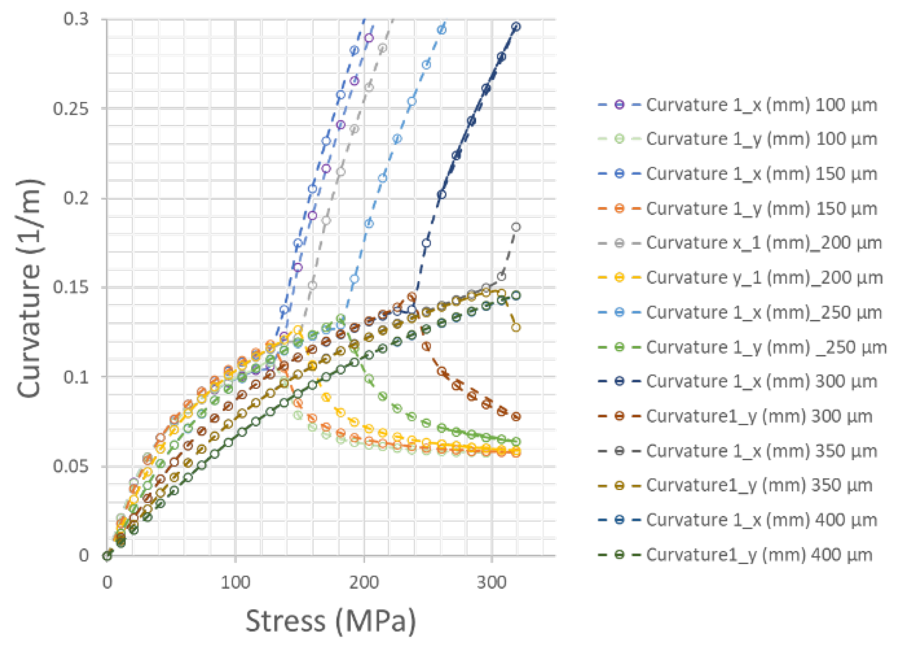
In Figure 3 we report the trend of the simulated curvature as a function of the stress, for a set of taiko wafers whose central substrate region thickness ranges from 100 µm to 400 µm. An asymmetry has been induced in the wafer by applying a slight force at the rim of the wafer, such that to ignite the bifurcation. We observe that, differently from Figure 2, as the stress reaches a critical value the taiko wafer bifurcates. Moreover, as we decrease the thickness of the central region the bifurcation point occurs at lower values of the FSM stress. The resulting graph is a bifurcation diagram, which can be of help in the comprehension of how to extend the concept of equivalent thickness to the bifurcated case.
Figure 2.
Curvature as a function of the stress for a taiko wafer, reported from ref. [2] with hs ranging in the interval 100 - 400 µm and the other quantities fixed to the typical value reported in table.
Figure 2.
Curvature as a function of the stress for a taiko wafer, reported from ref. [2] with hs ranging in the interval 100 - 400 µm and the other quantities fixed to the typical value reported in table.

Figure 3.
Bifurcation diagrams reporting the curvature as a function of the stress of the metal layer for a set of taiko wafers whose central substrate region thickness ranges from 100 µm to 400 µm. The bifurcation ignites for all the thickness in the range of the thickness investigated, except for the 400 µm case. The curvature at the bifurcation point, as well as its bifurcation stress increase with the thickness of the substrate.
Indeed, to further investigate the degeneration of this non-linear phenomenon, in Figure 4 we focused on the bifurcation diagram reporting the warpage of a FSM 200 µm taiko wafer as a function of the stress σ of the metal layer . The behavior of the taiko wafer is compared with a flat 200 µm Si/Al wafer. As we can see, the bifurcation in the case of a 200 µm thin flat wafer occurs at lower values of the stress, occurring above around 30 MPa. To fit the bifurcation diagram of the taiko wafer, we need to increase the thickness of the wafer up to 350 µm and set the thickness of the Al metal layer to 4.97 µm. Also in this case, with respect to the case of a plain wafer, the bifurcation is mitigated by the ring region.
In Figure 5a we report the top view of a snapshot of the directional deformation or warpage along the z direction of the 200 mm FSM taiko, 200 µm thin in the central region. Whereas Figure 5b reports the projected view of the same warped FSM taiko wafer. The wafer is bifurcated.
In Figure 6a,b we report a snapshot of the top and projected view of the bifurcated 200 mm plain taiko wafer for comparison, respectively. It is evident that in the case of the plain wafer the resulting warpage at bifurcation is higher with respect to the taiko wafer case reported in Figure 5a,b.
In Figure 7 we report the equivalent thickness in the linear regime of the investigated FSM taiko wafers as a function of the substrate thickness in the central region. These data, which are also reported in ref [2], are shifted by a thickness Δ of about 35 µm, since the 200 µm works as if the equivalent thickness in the bifurcation is higher of this quantity with respect to the linear regime.
Moreover, from theory [21] it is known that the bifurcation at the curvature is given by:
Hence, from the data of the equivalent thickness shifted by the thickness Δ we can gain a bifurcation curvature relative to the taiko wafer. In Table 2, we have reported the bifurcation curvatures as obtained from the simulated values reported in Figure 3, and the calculated bifurcation curvatures according to Equation (3), from the shifted data of the equivalent thickness in the linear regime, as reported in Figure 7.
It is worth plotting the resulting data from Table 2. In Figure 8 the and have been reported as a function of the substrate thickness. It is worth to observe as the bifurcation curvatures report the same trend and order of magnitude and agree better for those substrate thicknesses ranging from 100-250 µm. Instead, above 250 µm there are increasing deviations between the two values.
Conclusions
In conclusion, by using ANSYS simulation tools, we have investigated the occurrence of bifurcation in 8” taiko wafers. As in the case of the investigation of the warpage in the linear regime, also in this case the presence of the rim of the taiko wafer mitigates the degeneration of non-linear phenomena igniting the bifurcation. To understand better the phenomenon we defined, for a given thickness of the central region of the taiko wafer, an equivalent thickness in the bifurcation regime. In particular, in the case of 200 µm it results that such a thickness is 35 µm higher with respect to the linear regime equivalent thickness case. Hence, by shifting all the equivalent thicknesses of the same quantity of 35 µm, we gained a value of the bifurcation curvatures which can be compared with those obtained from the ANSYS simulations. It results that these values are roughly in agreement in the range of 100-250 µm. Hence Equation (3) can be a useful approximation of the equivalent thickness of a taiko wafer occurring at bifurcation, which in this case can be written as:
Author Contributions
V.V. Conceptualization of the work, analytical model elaboration, conceptualization of the ANSYS® simulation experiments, data elaboration, paper drafting, editing, and writing. G.L.M. ANSYS® system design, optimization and simulations. M.R. sponsorship, funding, validation. All authors have read and agreed to the published version of the manuscript.
Acknowledgment
It is acknowledged the Italian Ministry of Enterprises and Made in Italy (Ministero delle Imprese e del Made in Italy MIMIT) in the frame of the Important Project of Common European Interest (IPCEI) on Microelectronics and Communication Technologies.
References
- V. Vinciguerra and A. Landi, "On the Way to understand the Warpage in 8’ Taiko Semiconductor Wafers for Power Electronics Applications (Si and SiC)," in 2021 22nd International Conference on Thermal, Mechanical and Multi-Physics Simulation and Experiments in Microelectronics and Microsystems (EuroSimE), Virtual, 2021. [CrossRef]
- V. Vinciguerra, G. L. Malgioglio, A. Landi, M. Renna. Determination of the Equivalent Thickness of a Taiko Wafer Using ANSYS Finite Element Analysis. Appl. Sci. 2023, 13, 8528. [CrossRef]
- V. Vinciguerra, G. L. Malgioglio, A. Landi, S. Rascunà, M. Renna, A Comparative Study of Analytical and Finite Element Analysis Numerical Approaches of the Equivalent Thickness of Large 4H-SiC Taiko Wafers, Research Square preprint. [CrossRef]
- G. G. Stoney, "The tension of metallic films deposited by electrolysis," Proceedings of the Royal Society of London. Series A, Containing Papers of a Mathematical and Physical Character, vol. 82, no. 553, 1909. [CrossRef]
- G. C. Janssen, M. M. Abdalla, F. van Keulen, B. R. Pujada and B. van Venrooy, "Celebrating the 100th anniversary of the Stoney equation for film stress: Developments from polycrystalline steel strips to single crystal silicon wafers," Thin Solid Films, vol. 517, no. 6, pp. 1858-1867, 1 2009. [CrossRef]
- L. Freund, ((2000).). Substrate curvature due to thin film mismatch strain in the nonlinear deformation range,. Journal of the Mechanics and Physics of Solids, vol. 48, n. 6. [CrossRef]
- L. Freund, J. Flora, & E. Chason. (1999). Extensions of the Stoney formula for substrate curvature to configurations with thin substrates or large deformations. Applied Physics Letters, 74(14),. [CrossRef]
- C.B Masters, N. S. (1990). Deflection shapes due to intricsic stress in thin films. Mat. Res. Soc. Symp. Proc. Vol. 188, 1990, Materials Research Society. [CrossRef]
- C.B Masters, N. S. (1993). Geometrically Nonlinear Stress-Deflection Relations for Thin Film/SubstatSystems. Int. J. Engng Sci, Vol 31, No. 6, pp. 915-925. [CrossRef]
- D. Shin, J. L. (February 2014.). Analysis of Asymmetric Warpage of Thin Wafers on Flat Plate Considering Birfurcation and Gravitational Force. IEEE Transactions on Components, Packaging and Manufacturing Technology, Vol. 4, No 2. [CrossRef]
- V. Vinciguerra, A. Landi, G. L. Malgioglio. Wafer Bifurcation as a Spontaneous Symmetry Breaking. In Proceedings of the 23rd International Conference on Thermal, Mechanical and Multi-Physics Simulation and Experiments in Microelectronics and Microsystems (EuroSimE), St. Julian, Malta, 25–27 April 2022. [CrossRef]
- Abdelnaby, A. e. ((2013).). Numerical simulation of silicon wafer warpage due to thin film residual stresses. in IEEE Workshop on Microelectronics and Electron Devices, WMED,. [CrossRef]
- Mallik A and Stout, R. ,. ((2010).). Simulation of process-stress induced warpage of silicon wafers using ANSYS® finite element analysis. in 43rd International Symposium on Microelectronics 2010 IMAPS, (2010). [CrossRef]
- Mallik, A., Stout, R., & Ackaert, J. (2014). Finite element simulation of different kinds of wafer warpages: Spherical, cylindrical, and saddle. IEEE Transactions on Components, Packaging and Manufacturing Technology, 4(2), 240 - 247. [CrossRef]
- Schicker, J., Khan, W., Arnold, T., & Hirschl, C. (2016). Simulating the warping of thin coated Si wafers using Ansys layered shell elements. Composite Structures, 140. [CrossRef]
- V. Vinciguerra, G. L. Malgioglio, A. Landi, Modelling the Elastic Energy of a Bifurcated Wafer: A Benchmark of the Analytical Solution vs. The ANSYS Finite Element Analysis. Compos. Struct. 2022, 281, 114996. [CrossRef]
- V. Vinciguerra, M. Boutaleb, G. L. Malgioglio, A. Landi, F. Roqueta, M. Renna, Investigating the Occurrence of Bifurcation in Large Metalized Wafers using ANSYS [1] Layered Shell Elements. In Proceedings of the 2023 24th International Conference on Thermal, Mechanical and Multi-Physics Simulation and Experiments in Microelectronics and Microsystems (EuroSimE), Graz, Austria, 16–19 April 2023. [CrossRef]
- V. Vinciguerra, G. L. Malgioglio, A. Landi, A.; M. Renna, Models of Bifurcation and Gravity Induced Deflection in Wide Band Gap 4H-SiC Semiconductor Wafers. In Proceedings of the 2023 24th International Conference on Thermal, Mechanical and Multi-Physics Simulation and Experiments in Microelectronics and Microsystems (EuroSimE), Graz, Austria, 16–19 April 2023. [CrossRef]
- V. Vinciguerra, G. L. Malgioglio and A. Landi, "Models of Bifurcation in a Semiconductor Wafer: A Comparison of the Analytical Solution vs. the ANSYS Finite Element Analysis," 2022 23rd International Conference on Thermal, Mechanical and Multi-Physics Simulation and Experiments in Microelectronics and Microsystems (EuroSimE), St Julian, Malta, 2022, pp. 1-4. [CrossRef]
- V. Vinciguerra, G. L. Malgioglio, A. Landi, S. Valastro, B. Cafra, M. Renna. From Wafer Bifurcation to Warpage Die: A Correlation Method to determine the Warpage of a Metal-Coated Silicon Substrate. In Proceedings of the 2022 23rd International Conference on Thermal, Mechanical and Multi-Physics Simulation and Experiments in Microelectronics and Microsystems (EuroSimE), St. Julian, Malta, 25–27 April 2022. [CrossRef]
- L.B. Fruend, S. Suresh. (2004). Thin Film Materials: Stress, Defect Formation and Surface Evolution. Cambridge: Cambridge University Press.
Figure 1.
On the left, schematic of a front side metalized taiko wafer. On the right cross section of a front side metal (FSM) taiko wafer illustrating the quantities determining the warpage of the FSM taiko wafer. is the internal radius, external radius, thickness of the substrate and the height of the ring. The FSM taiko wafer is subject to radial and circumferential forces at the FSM/substrate interface, whose value per unit length are Fr and Fθ, respectively. The wafer is supported at the external ring and Nr and Nθ are the radial and circumferential reaction forces per unit length. The front of the wafer is at with respect to the neutral plane. The step height is fixed and put equal to .
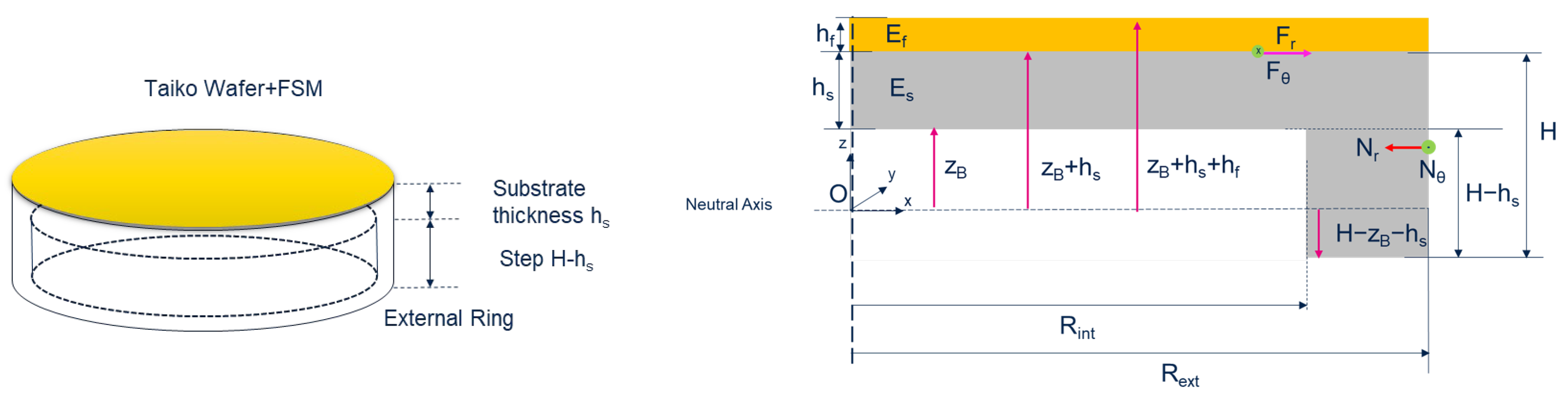
Figure 4.
Bifurcation diagram reporting the warpage of an FSM 200 µm taiko wafer as a function of the stress σ of the metal layer. The behaviour of the taiko wafer is compared with a flat 200 µm Si/Al wafer and with the case of flat Si/Al having a thickness of the silicon layer of 350 µm and of the Al metal layer of 4.97 µm.
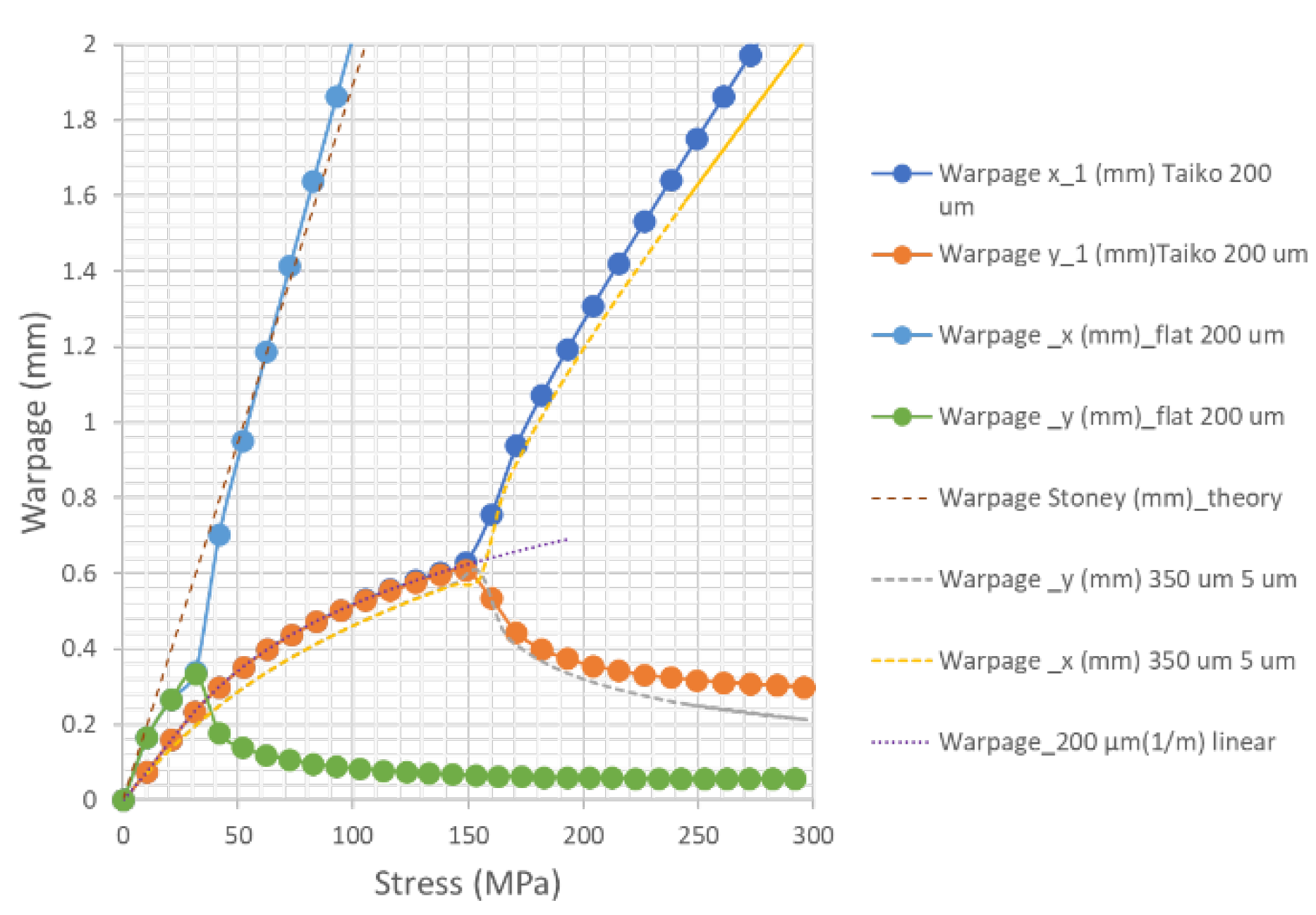
Figure 5.
(a). Top view of the directional deformation of a bifurcated taiko wafer simulated at a nominal temperature of T = 100 °C. The substrate region has a thickness of 200 µm, the step height is of 450 µm. (b). rojection of the directional deformation of the same bifurcated taiko wafer simulated at a nominal temperature of T=100 °C. The substrate region has a thickness of 200 µm, the step height is of 450 µm. Magnification 100 ×.
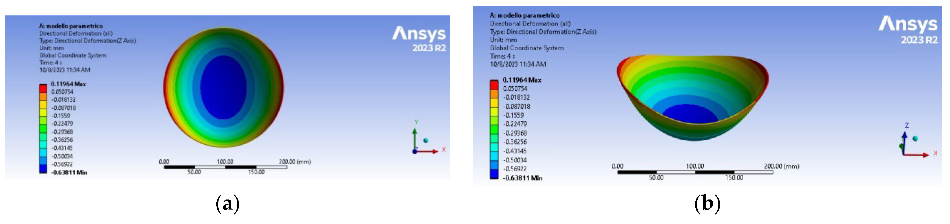
Figure 6.
(a). Top view of the directional deformation of a flat wafer simulated at a nominal temperature of T = 55 °C. The substrate region has a thickness of 200 µm. (b). Projected view of the same flat 200 µm wafer. Magnification 100 ×.
Figure 6.
(a). Top view of the directional deformation of a flat wafer simulated at a nominal temperature of T = 55 °C. The substrate region has a thickness of 200 µm. (b). Projected view of the same flat 200 µm wafer. Magnification 100 ×.
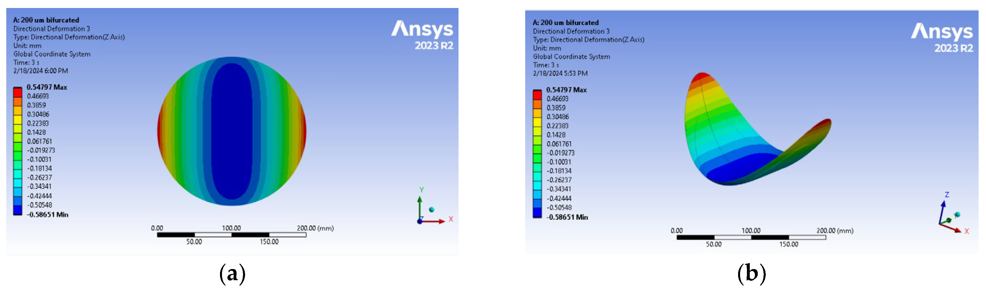
Figure 7.
Equivalent thickness of a FSM taiko wafer in the linear regime, as reported in reference [2], as a function of the central substrate thickness of the taiko wafer translated by a thickness Δ of about 35 µm, resulting from the investigation of the 200 µm case reported in Figure 4.
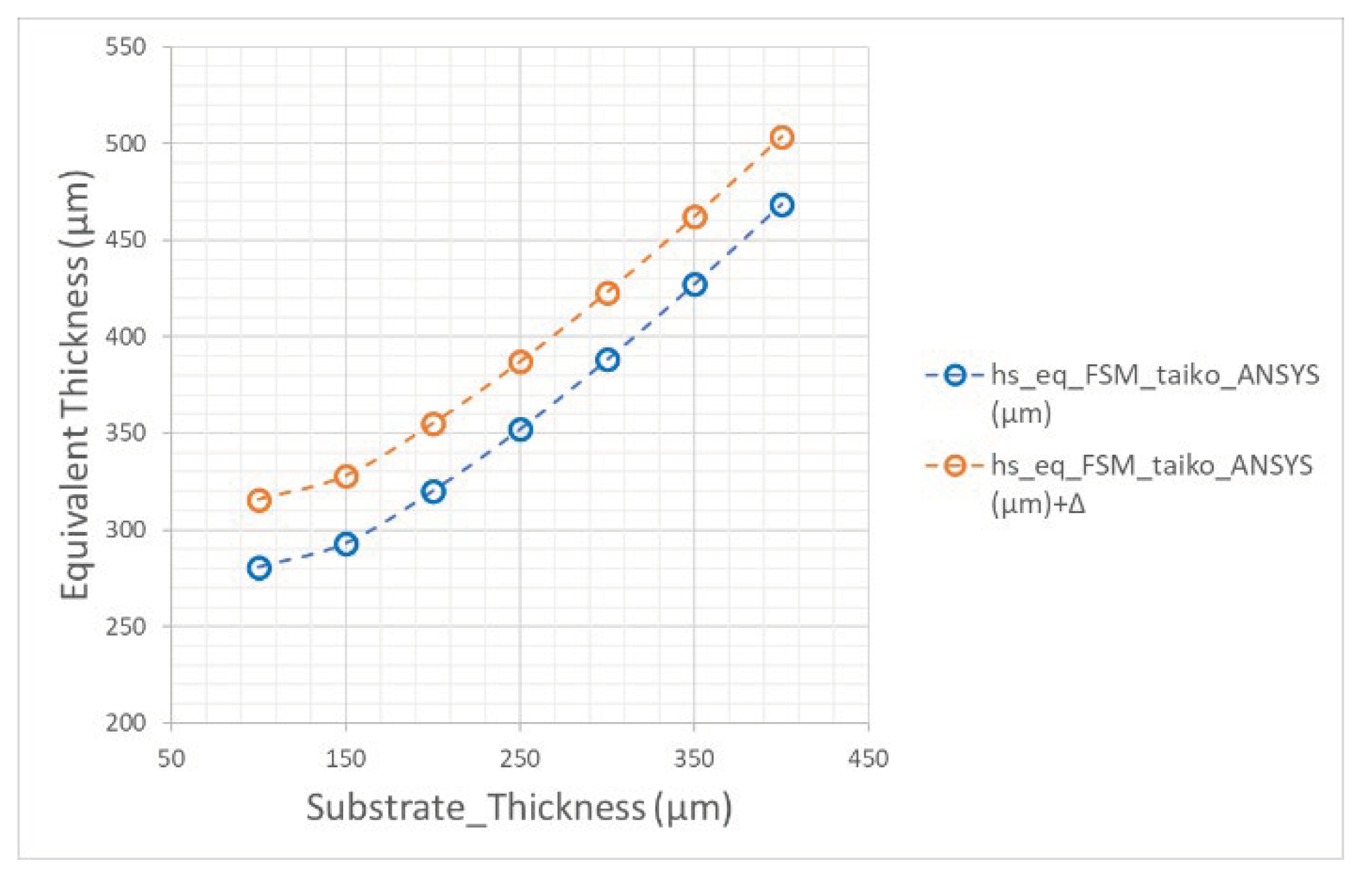
Figure 8.
and gained from Table 2 as a function of the substrate thickness.
Figure 8.
and gained from Table 2 as a function of the substrate thickness.
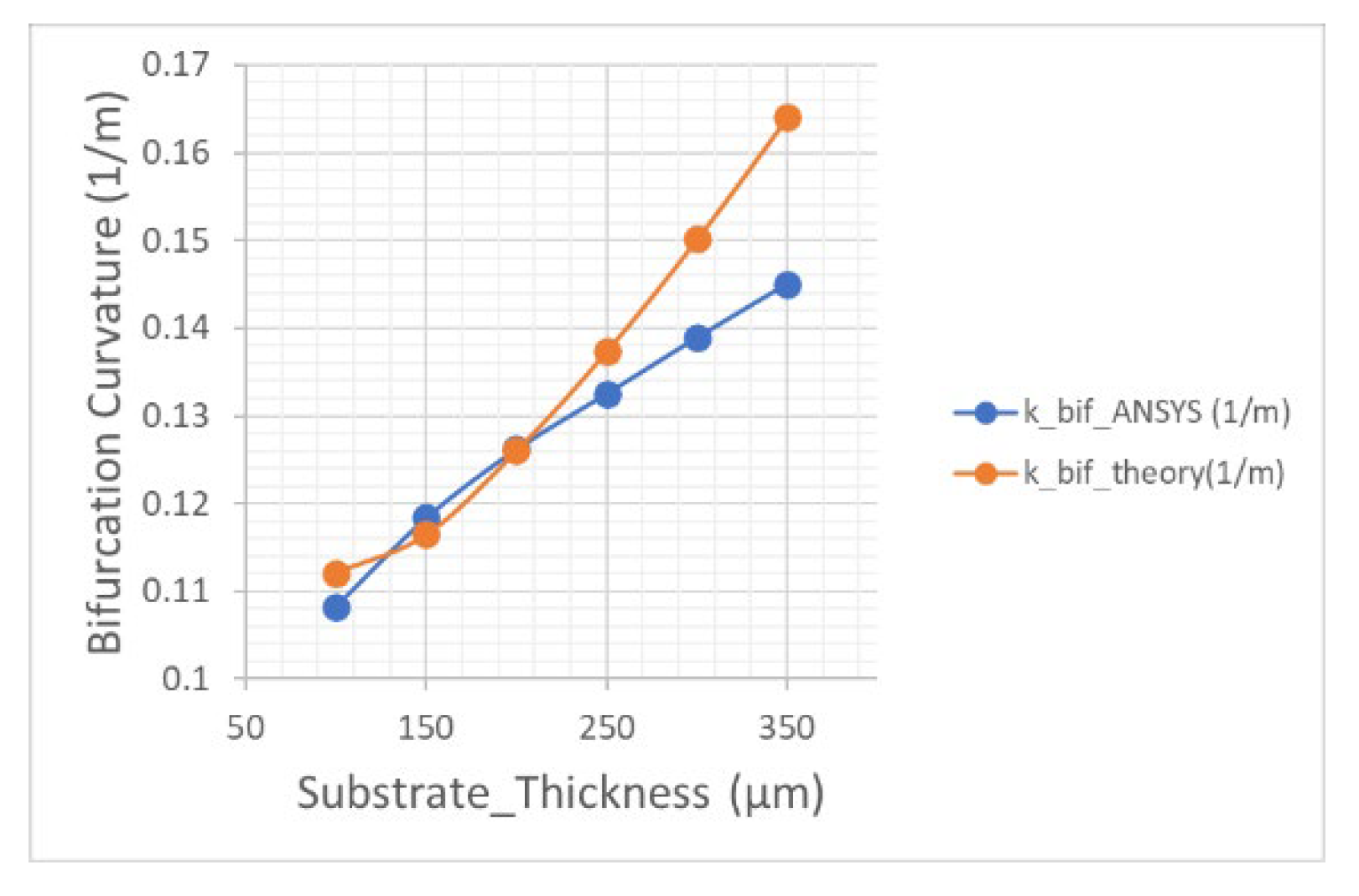

Table 1.
Table reporting the typical value of the geometrical properties of the investigated FSM-taiko wafer.
Table 1.
Table reporting the typical value of the geometrical properties of the investigated FSM-taiko wafer.
| Symbol | Quantity | Typical Value |
|---|---|---|
| Substrate Thickness (µm) | 200 | |
| Step Height (µm) | 450 | |
| Front Side Metal Thickness (µm) | 4.5 | |
| Ring Width (mm) | 3.7 |
Table 2.
Values of the bifurcation curvatures, obtained from the data reported in Figure 3, as a function of the substrate thickness of the taiko wafer and the theoretical value gained from Equation (3).
Table 2.
Values of the bifurcation curvatures, obtained from the data reported in Figure 3, as a function of the substrate thickness of the taiko wafer and the theoretical value gained from Equation (3).
| Substrate thickness (µm) | k_bif_ANSYS (m-1) | k_bif_theory (m-1) |
|---|---|---|
| 100 | 0.108 | 0.112 |
| 150 | 0.118 | 0.116 |
| 200 | 0.126 | 0.126 |
| 250 | 0.133 | 0.137 |
| 300 | 0.139 | 0.150 |
| 350 | 0.145 | 0.164 |
Disclaimer/Publisher’s Note: The statements, opinions and data contained in all publications are solely those of the individual author(s) and contributor(s) and not of MDPI and/or the editor(s). MDPI and/or the editor(s) disclaim responsibility for any injury to people or property resulting from any ideas, methods, instructions or products referred to in the content. |
© 2024 by the authors. Licensee MDPI, Basel, Switzerland. This article is an open access article distributed under the terms and conditions of the Creative Commons Attribution (CC BY) license (http://creativecommons.org/licenses/by/4.0/).
Copyright: This open access article is published under a Creative Commons CC BY 4.0 license, which permit the free download, distribution, and reuse, provided that the author and preprint are cited in any reuse.


