1. Introduction
Neutrino astronomy has entered a fruitful era with the success of neutrino telescopes. The IceCube Telescope [1] has confirmed the presence of high-energy cosmic neutrinos, correlated a high-energy neutrino with a transient source [2], and has even detected neutrinos from a steady source, NCG 1068 [3]. KM3NeT [4], currently under construction, will focus on finding cosmic neutrino sources in the new multi-messenger era, potentially solving the mystery of high-energy cosmic rays’ origin. This places KM3NeT alongside IceCube at the forefront of many exciting physics topics. Improving the angular resolution of neutrino telescopes is crucial for pinpointing steady point-like sources [5]. The use of Silicon PhotoMultipliers (SiPMs) [6] in the next generation of telescopes, either alone or in combination with PhotoMultiplier Tubes (PMTs), will greatly enhance the angular resolution [8]. About 40 % improvement in the angular resolution could be reached in seawater by the use of a hybrid detection node composed of SiPMs and PMTs, while in ice the improvement could be around 20 % because of the higher light scattering. This increases the likelihood of detecting steady point-like sources. SiPMs offer rapid responses and low jitter, crucial for improving angular resolution. The rise time of SiPM pulses is about a quarter of a nanosecond. The transit spread time of SiPM signals has a similar value, which significantly improves those of PMTs, which in the case of KM3NeT PMTs are over the nanosecond. Additionally, ice telescopes could benefit from SiPMs’ advantages, including higher photon efficiency and larger detection area. Nevertheless, equipping neutrino telescopes with SiPMs poses a technological challenge, particularly in dealing with their high dark count rate (DCR). After pulses, delayed signals generated by SiPMs, can also affect system performance. A technique to mitigate these effects, based on coincidences, is presented in this work.
This work begins by discussing the advantages and disadvantages of using SiPMs in neutrino telescopes in
Section 2. In
Section 3, the problems of SiPM DCR are discussed. The DCR filter proposed in this work is presented in
Section 4, while the implementation of the filter is discussed in
Section 6 and the first results are presented in
Section 5, followed by the conclusions in
Section 7.
2. SiPMs in Neutrino Telescope: advantages and disadvantages
SiPMs consist of a Geiger mode avalanche photodiode array on a common silicon substrate [12], typically housing 1000 microcells (pixels) in a 1 mm2 area. Each pixel behaves akin to a photodiode and a quenching resistor in series, ensuring a uniform response. With rise times under a quarter of a nanosecond [6,9] and time transit spreads (TTSs) of similar values [6,10], SiPMs are well-suited for the next generation of neutrino telescopes. Using SiPMs in neutrino telescope acquisition nodes, whether in lieu of or alongside PMTs, can significantly enhance angular resolution [8], improving the precision of neutrino telescope readings [5]. Nevertheless, the acquisition electronics requirements go beyond the traditional 1-ns resolution [11]. Beyond their precise timing, SiPMs offer various advantages for neutrino telescopes:
Sensitivity spanning the ultraviolet to near-infrared, ideal for Cherenkov light.
No need for a high voltage supply exceeding 100 V, yet comparable gains to traditional PMTs (105–106) are achieved.
Immunity to electromagnetic fields.
The SiPMs can be packed, being it possible to make adjustable expansions at a relatively lower cost compared to PMTs [13].
Excellent single photon resolution [14].
Mechanically more robust than PMTs.
Resilience to stray light due to solid-state technology.
High photon detection efficiency (PDE), exceeding 50% in blue [15], compared to 30% in KM3NeT PMTs [16].
Abundance of producers in this growing market with associated R&D [17,18].
The characteristics of SiPMs lead to improved efficiency, detection area, directional sensitivity, and overall angular resolution. On the other hand, the main disadvantage of SiPMs for their use in neutrino telescopes is their extremely high DCR.
3. SiPM Dark Count Rate challenge
SiPMs could improve the performances of neutrino telescopes, nevertheless, they exhibit a notably high DCR, surpassing the capabilities of current neutrino telescope acquisition systems. Although DCR has dropped from 1 MHz/mm
2 to below 40 kHz/mm
2 at ambient temperature in recent years, it remains substantially higher than in PMTs, posing a challenge for their integration in neutrino telescopes. For comparison, PMTs in KM3NeT have an average dark noise of about 0.28 Hz/mm
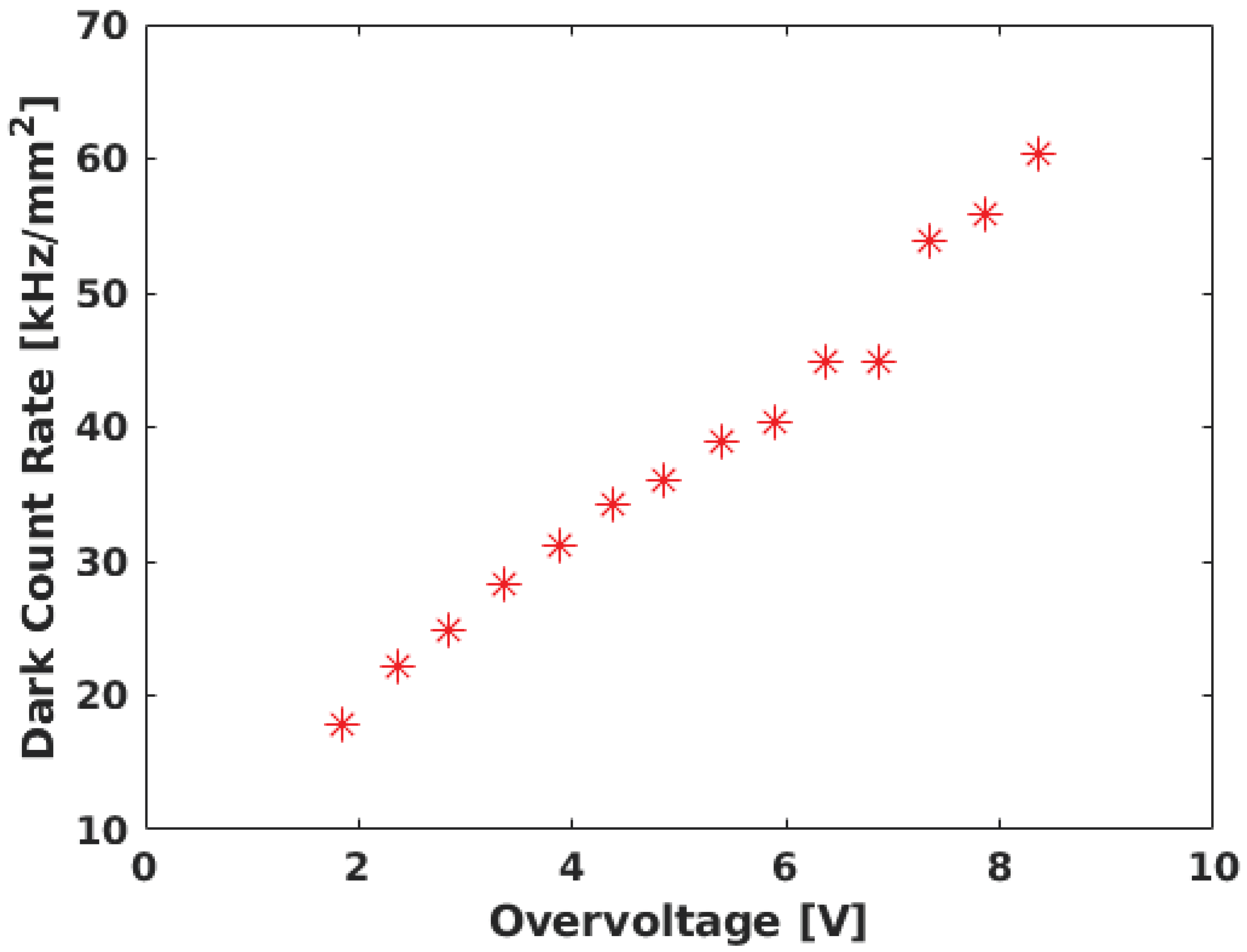
2 [16], over five orders of magnitude lower than SiPMs. SiPM DCRs arise from thermal carrier generation, trap-assisted tunneling, or band gap tunneling, resulting in a response equivalent to a single photon. The DCR is highly temperature-dependent, halving its value every eight degrees [19]. Presently, state-of-the-art SiPMs exhibit a DCR of about 20–30 kHz/mm
2 [20] at ambient temperature (see
Figure 1), a challenge for the acquisition system that has thus far hindered their implementation in neutrino telescopes. At these noise rates, a SiPM with a detection area similar to that of a multi-PMT Digital Optical Module (DOM) [21] at seawater temperature would yield a DCR of approximately 30 MHz. This level of noise surpasses the capabilities of current readout systems, leading to communication bandwidth overload. While operating underwater, the temperature reduction would halve the SiPM DCR [23], and in the case of ice, it reduces by about two orders of magnitude [24]. However, the noise level remains significant. Implementing a threshold above a single photoelectron could result in a 100-fold reduction in the DCR [6], albeit at the cost of losing single-photon event information. Therefore, it is imperative to incorporate a DCR rejection technique within the acquisition electronics.
4. DCR Filtering
The state-of-the-art detection node in neutrino telescopes is composed of a glass sphere embedding several tens of Photomultipliers [7,21]. The acquisition front-end electronics of the first of this multi-PMT DOM [22], developed for KM3NeT, converts the PMT analog pulses into a digital signal, which is active during the time the PMT signal is over a threshold, the Time over Threshold (ToT). The ToT signals are transmitted to a central acquisition board, which main FPGA implements the TDCs. The TDCs time stamp the arrival time of the ToT pulses and measure the duration of the ToT. All the information acquired is sent on-shore for further analysis, the so-called "all-data-to-shore" approach. An improvement of the multi-PMT DOM involves the use of SiPMs together with PMTs. The main problem of using SiPMs is the high DCR of SiPMs which would saturate the bandwidth available. One potential approach in neutrino telescopes involves reducing the DCR by enhancing the "all-data-to-shore" scheme through the implementation of a coincidence filter between channels in the acquisition electronics and therefore not sending all the data but only the most relevant fraction.
Figure 2 shows a simplified scheme of how the acquisition system could be, with two acquisition channels, one with PMT, acting as a trigger channel, and another with a SiPM. The analog pulses are digitized by the front-end electronics, converted into a ToT pulse, and sent to the acquisition board to be acquired by the TDCs, which timestamp the arrival time of the ToT pulse and measure its width. Using only SiPMs as triggering channels will not reduce the DCR significantly, as coincidences of DCR pulses will not be filtered. A SiPM 1 MHz trigger signal, with a triggering window of 12 ns, would imply about 1.2 % or 0.12 MHz of coincidences or false positives with a SiPM channel with the same DCR. While the false positives are not a problem by themselves as higher levels of trigger will reject them, the high rate would saturate the bandwidth available, and therefore a hybrid DOM composed of PMTs for triggering SiPMs is the best approach for neutrino telescopes. The 31 PMTs of the KM3NeT Multi-PMT DOM can be extended with several SiPMs (about 16) in the interstices of the PMTs. This implementation would lead to a higher detection area and higher directivity, as the DOM will have more detection segments. In addition, the SiPMs provide better timing. In this hybrid DOM, a DCR filter could be used, using the PMT signals as triggers of the SiPM channels. The inclusion of a coincidence filter in the readout electronics is essential for reducing the substantial DCR produced by SiPMs and ensuring that the data sent to the central station remains within the available bandwidth. The drawback of this implementation is the cases when the SiPMs detect photons but the triggering PMT does not, as the SiPM signal will be filtered. The configurable time window for the filtering process, with a default value (12 ns) similar to the trigger window used in the KM3NeT DOM trigger, adds an element of adaptability as it is possible to adapt this window to the operation conditions. The processing of acquired data to perform coincidences within the acquisition electronics, which will effectively reduce the data rate destined for the central station, is one of the pivotal factors in reducing the DCR, and therefore being able to use SiPMs for enhancing the angular resolution of neutrino telescopes. The incorporation of Field-Programmable Gate Arrays (FPGAs) would confer extra flexibility, allowing for remote upgrades of the DCR filter, even with the detection nodes already deployed. It is important to embed the TDCs and the DCR filter in the same device, as a fast communication between them is mandatory for the filtering of the DCR.
|
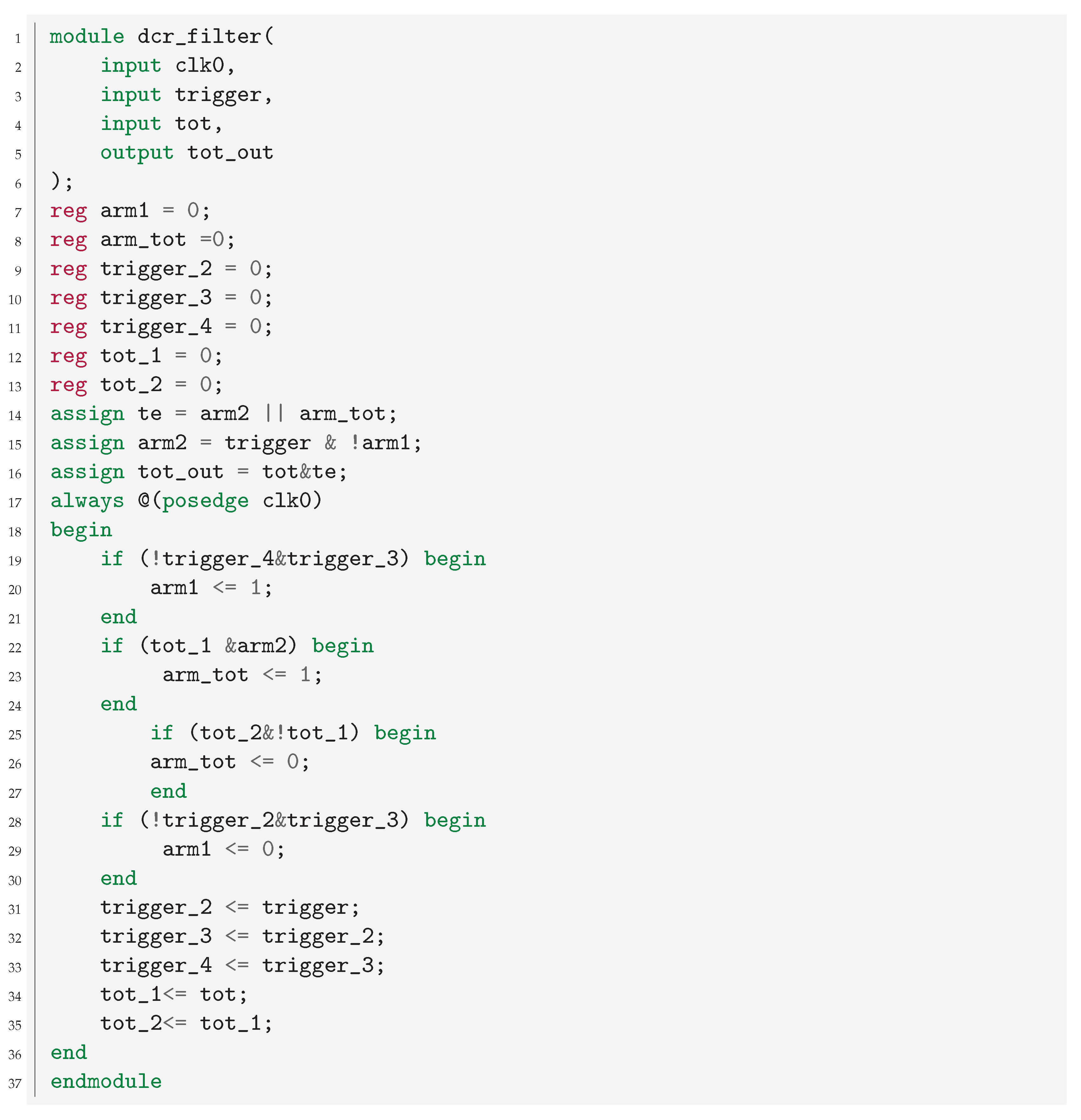
Listing 1. Verilog implementation of the DCR filter testbench. If an event enters during the 12 ns-window, the full event is acquired. |
 |
The implementation of the TDCs and the DCR filter are discussed in this section, together with the testbench where the validation of the DCR filter has been performed.
4.1. TDC implementation
To implement and test the DCR filter, a 1-ns TDC has been implemented. The architecture of the TDCs is multi-phase shift clock in order to reduce the resources used, which is of paramount importance in neutrino telescopes applications due to the operation conditions. Four phases of 250 MHz shifted 90° are used. The change of clock domain is obtained in four steps, instead of the three used in other implementations, to guarantee that there are no timing issues. The implemented TDC also allows for an easy integration with the DCR filter.
4.2. DCR filter implementation
The filter of the DCR should be implemented using very low resources. The acquisition of all the events and posterior filter requires a significant amount of resources. It needs a huge buffer and the events require to be ordered, which requires a significant use of computation resources. Both requirements are not available in neutrino acquisition systems, so a lower resource architecture is needed. While the DCR filter reduces the bandwidth needed, the resources used should be kept as low as possible, which limits the complexity of the filter. The filtering should be done when the data are organized and this only happens when they arrive. This is the approach taken in this work. The SiPM signals are rejected by default and only when a PMT signal occurs, which acts as a trigger, the acquisition of SiPMs is allowed. As the acquisition of all the channels are in the same FPGA there are no timing problems. The behavior of the DCR filter is exemplified in the timeline of
Figure 7. The input from the slave TDC is intentionally delayed 2.5 ns to anticipate the arrival of the PMT signal, which would be detected by the master TDC. This delay can be implemented either in the FPGA (as in the present case), in the transmission line from the SiPM to the acquisition electronics, or with a combination of the two previous cases. A trigger window of 12 ns is initiated by a rise in the master input signal. If an event is detected in the slave TDC during this short window (i.e. light arrives at the SiPM), it is read out. Events starting before the trigger window is open and active during the trigger window are acquired since the trigger window opens and until the end of the input pulse. Finally, slave-TDC events occurring outside of this 12 ns window are rejected and are not acquired. The Verilog code of the filter is presented in Listing 1.
4.3. Test bench implementation
The test has been implemented in a Xilinx evaluation board, the Zedboard
1, which has an ARTIX-7
2 FPGA of 85k Logic cells and a speed rate -1. In order to test the DCR filter, two TDC channels are embedded in the FPGA. One of the TDC channels acts in master mode, which would correspond with the Photomultiplier Tube (PMT) channel, and one in slave mode, corresponding to the SiPM channel. The TDC Intellectual Property core implements an Advanced eXtensible Interface (AXI)-Stream slave and the TDC data are transferred to the Double Data Rate Memory using a Direct Memory Access controller and two of the High-Performance AXI ports of the processor included in the FPGA. The delay of the slave TDC is implemented with the IODELAYE2
3 primitive. The DCR filter is located just before the SiPM TDC channel. The resources consumed by the DCR filter are just one slice lookup table and two slice registers by DCR-filter channel.
5. First results
Two different tests have been performed to validate the DCR filter proposed.
5.1. Test with FPGA-generated input pulses
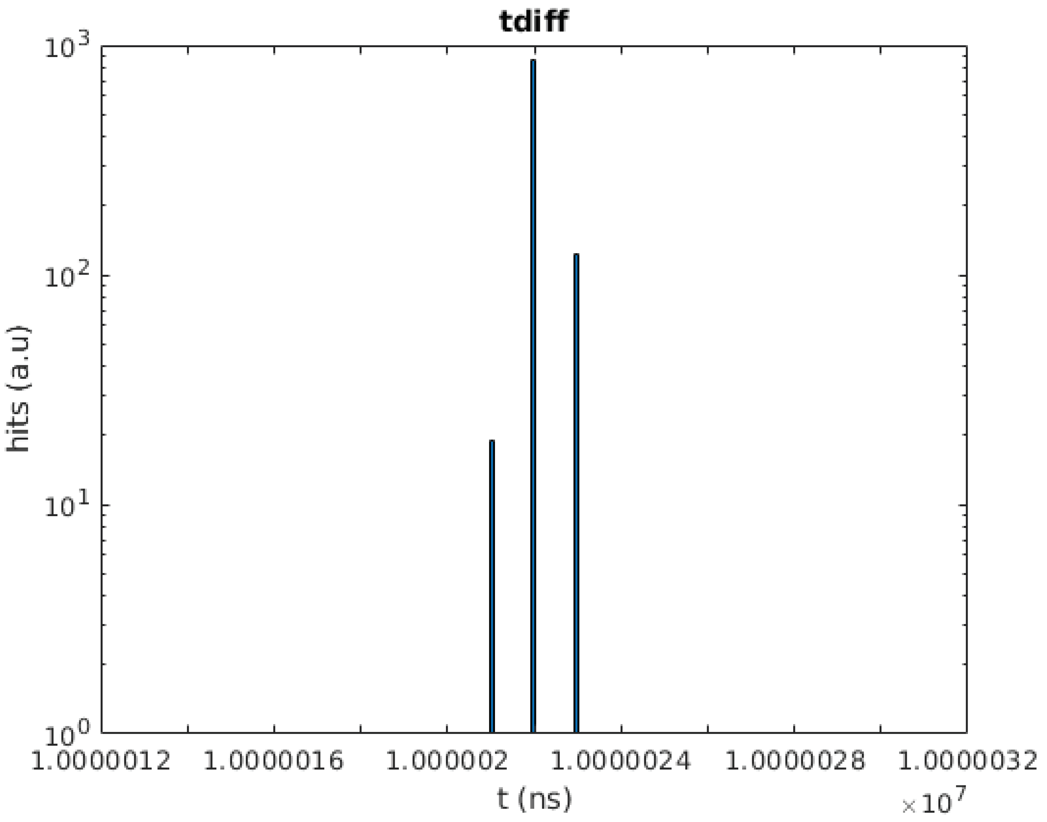
In the first test, the PMT and the SiPM signals are generated internally in the FPGA. To test the DCR filter with realistic input signals, first, the master channel is supplied with a pulse with a width of 40 ns and a frequency of 100 Hz. The second channel is supplied with the same 40 ns pulse as well as a simulated DCR pulse with a width of 40 ns and a frequency of 1 MHz.
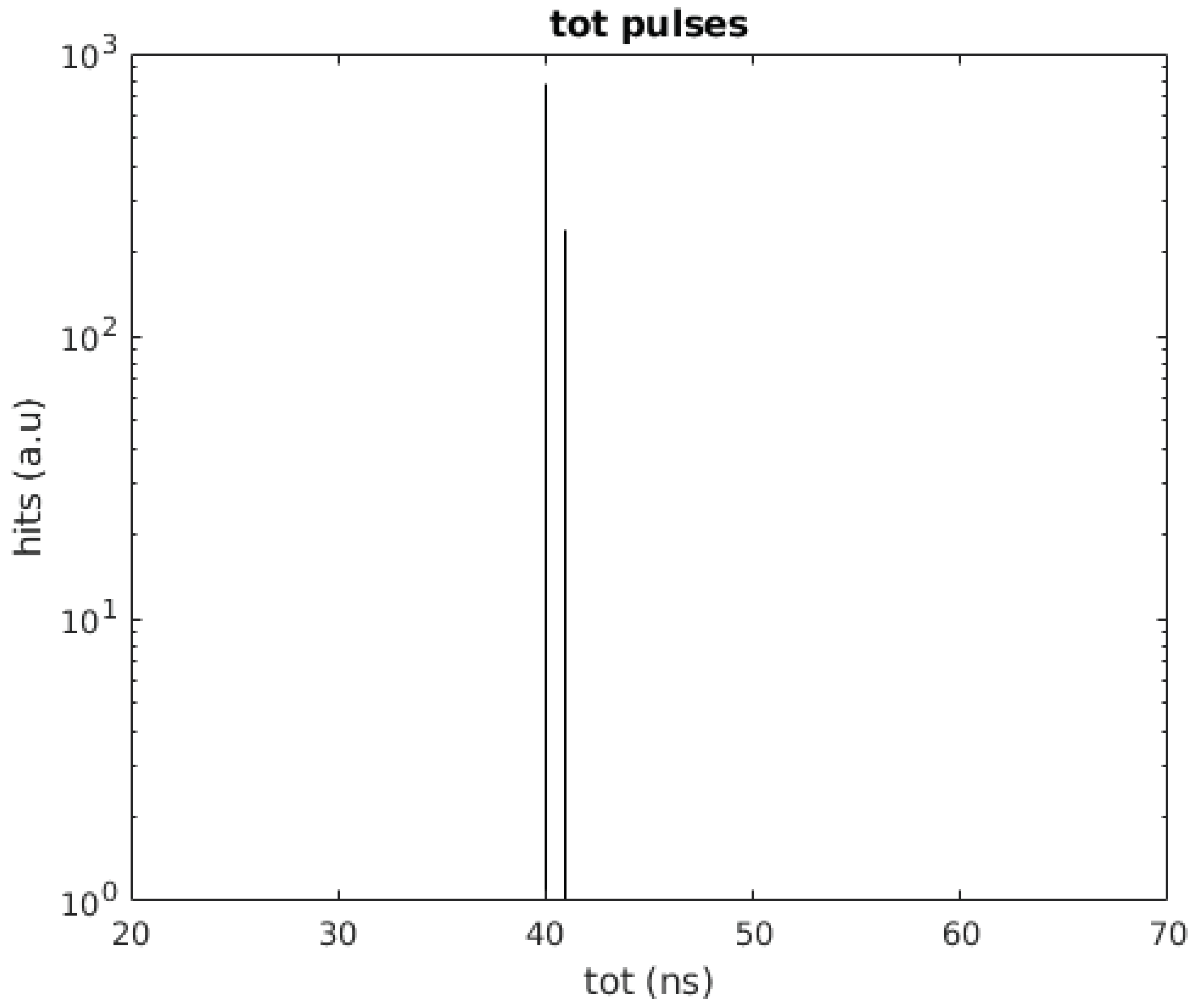
Figure 3 shows the test scheme implemented. The 100-Hz pulse emulates the arrival of single photons at both, the PMT and SiPM, and is the pulse that should be read out. The pulse width selected is about 15 ns longer than the typical KM3NeT ToT for single photoelectrons, which is 25 ns, although is still valid, provided that the ToT depends on the front-end electronics and the chosen threshold. The same applies to the SiPM. The 1-MHz pulse simulates the DCR of the SiPM, which has a signature equal to the single photoelectron signal, and it is added to the SiPM photon signal before arrival to the TDC in a similar way as happens in a SiPM. The results obtained for these tests are shown in
Figure 4 and
Figure 5. The filter effectively removes the DCR pulses in the SiPM TDC channel while maintaining the light pulses as it can be seen that the time difference between consecutive pulses registered by the SiPM TDC channel is 10 ms, the frequency of the simulated light pulses.
6. Implementation
6.1. Test with external pulse generator
In the second test, the simulated light pulse is generated by an external pulse generator. The phase of the external pulse generator is not correlated with the phase of the FPGA clock, so the coincidences between the simulated PMT signal and the SiPM signals are purely random. This is similar to the use of an external pulse generator to qualify the non-linearities of Time to Digital Converters using a
statistical code density test [
25,
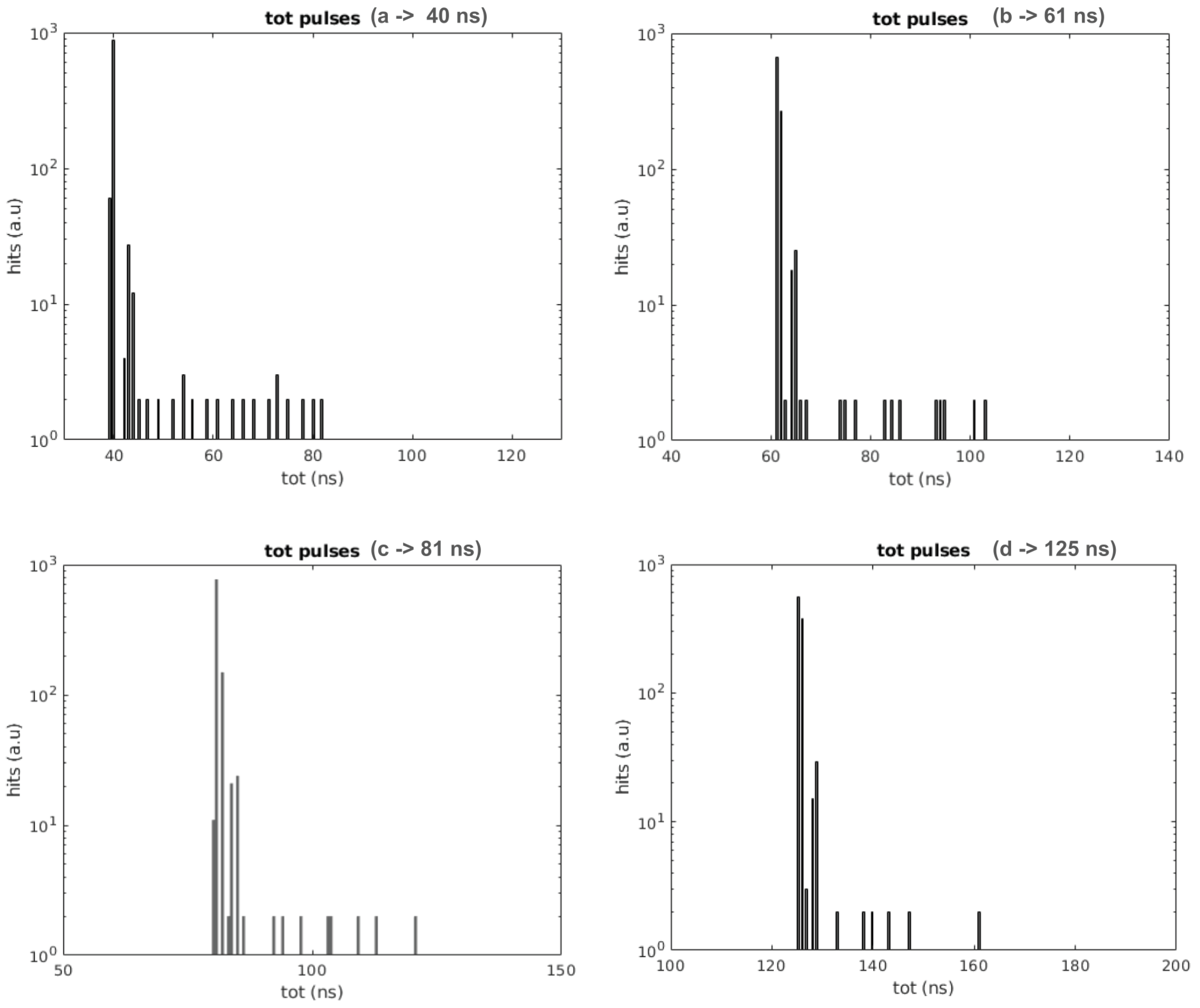
26]. An AWG.4022 from Active Technologies with an electrical rise time of 800 ps is used to that end. Four pulse widths have been tested, one at 40 ns as in the previous test, and the other three at 61, 81, and 125 ns, simulating signals generated by more than one photon. The results, which again show that the 40 ns DCR pulse is removed, are presented in
Figure 6. In the four cases, it is possible to see that there are a few pulses with longer duration than the photon pulse. The DCR pulse adds, in some cases, to the photon pulse, extending the total duration of the pulse. As can be seen, the total duration does not exceed the photon pulse length plus the DCR pulse length. This is not observed in the internally generated photon pulse (see previous section) as they are correlated to the DCR pulses, and in the case they superpose, they superpose completely. The addition of the DCR pulse can happen at the end or the beginning of the photon pulse. In the case it is added at the end of the photon pulse, there is an extension of the ToT, which can be extended up to the maximum possible, that is the photon pulse plus the DCR pulse. In the case in which the DCR pulse is added at the beginning of the pulse, it happens as in case two of the timeline presented in
Figure 7: The DCR part of the pulse is almost completely rejected and only remains the photon pulse plus the delay of the DCR filter. The small accumulation of ToTs with a length of about 3 ns longer than the photon pulses corresponds to this effect. In all cases, the DCR pulses are rejected.
Figure 6.
Results obtained when an external pulse generator is used to simulate the photon signals at the PMT and SiPM TDCs. A 30-ns pulse DCR at 1 MHz is simulated with an internal FPGA pulse generator. For light pulse length have been tested, at 40 (a), 61 (b)), 81 (c) and 125 ns (d). As can be observed, the DCR is, as expected, correctly filtered in all cases. There are some pulses with a longer duration with respect to the photon pulse. In these cases, the DCR adds to the photon signal resulting in a longer ToT. The maximum ToT observed corresponds to the light ToT plus the DCR ToT pulse.
Figure 7.
Timeline of the DCR-filter behavior. Three different cases are shown, cases one and three in blue, and case two in red. The trigger of the DCR filter is given by the PMT Pulse Input, which opens a
Trigger Window of 12 ns. If a SiPM Pulse occurs during the Trigger Window (case 1), the output of the filter is the same pulse. If the SiPM Pulse occurs just before the opening of the trigger window (case 2),
then the output of the pulse is the part of the pulse just after the opening of the Trigger Window. And finally, if the SiPM pulse is outside the Trigger Window, then the SiPM pulse is completely rejected
7. Conclusions
A filter architecture to reject the DCR of SiPMs installed in neutrino telescope nodes has been presented. PMT channels are used to trigger the SiPM channels, only allowing the readout of SiPM data during a small trigger window coincident with the detection of light by PMTs. The DCR filter includes a delay of the SiPM or slave channel to allow the trigger to arrive before an event in the slave channel appears. If an event arrives in the slave channel while the acquisition window is open, the full event is acquired. A proof of concept of the DCR filter, with two TDC channels, one in slave mode and the other in master mode, has been implemented and tested, achieving a complete rejection of the simulated DCR. The present development paves the way for the use of SiPMs in neutrino telescopes, which would improve the angular resolution. Future work will include an increase in the number of channels up to 32 masters and 32 slaves and the use of different filter schemes.
Acknowledgment
The authors acknowledge the financial support of the MCIN for PID2021-124591NB-C41, -C42, -C43, funded by MCIN/AEI/10.13039/501100011033 and by “ERDF A way of making Europe”, for ASFAE/2022/014, ASFAE/2022 /023 and AST22_6.2, with funding from the EU NextGenerationEU (PRTR-C17.I01), Generalitat Valenciana and Junta de Andalucía, and for CSIC-INFRA23013, Generalitat Valenciana for PROMETEO/2020/019, for CIDEGENT/2018/034, /2019/043, /2020/049, /2021/23 and for GRISOLIAP/2021/192 and EU for MSC/101025085, Spain.
References
- Aartsen, M.G.; et al. The IceCube Neutrino Observatory: Instrumentation and Online Systems. JINST 2017, 12, P03012. [Google Scholar] [CrossRef]
- Aartsen, M.G.; et al. Multimessenger observations of a flaring blazar coincident with high-energy neutrino IceCube-170922A. Science 2018, 361, eaat1378. [Google Scholar] [CrossRef]
- Abbasi, R.; et al. Evidence for neutrino emission from the nearby active galaxy NGC 1068. Science 2022, 378, 538–543. [Google Scholar] [CrossRef] [PubMed]
- Adrian-Martinez, S.; et al. Letter of intent for KM3NeT 2.0. J. Phys. G 2016, 43, 084001. [Google Scholar] [CrossRef]
- Fang, K.; et al. Identifying Ultrahigh-Energy Cosmic-Ray Accelerators with Future Ultrahigh-Energy Neutrino Detectors. JCAP 2016, 12, 17. [Google Scholar] [CrossRef]
- Acerbi, F.; Gundacker, S. Understanding and simulating SiPMs. Nucl. Instrum. Meth. A 2019, 926, 16–35. [Google Scholar] [CrossRef]
- Basu, V. [Icecube-Gen2] A multi-PMT optical sensor for IceCube-Gen2. JINT 2021, 16, 11 C11009. [Google Scholar]
- Hu, F.; Li, Z.; Xu, D. Exploring a PMT+SiPM hybrid optical module for next generation neutrino telescopes. PoS 2021, ICRC2021, 1043. [Google Scholar] [CrossRef]
- Saveliev, V. Silicon Photomultiplier - New Era of Photon Detection. In Advances in Optical and Photonic Devices; Kim, K.Y., Ed.; IntechOpen: Rijeka, Croatia, 2010; Chapter 14. [Google Scholar] [CrossRef]
- Acerbi, F.; Ferri, A.; Gola, A.; Cazzanelli, M.; Pavesi, L.; Zorzi, N.; Piemonte, C.; et al. Characterization of Single-Photon Time Resolution: From Single SPAD to Silicon Photomultiplier. IEEE Trans. Nucl. Sci. 2014, 61, 2678–2686. [Google Scholar] [CrossRef]
- Aiello, S.; Albert, A.; Alves Garre, S.; Aly, Z; Ameli, F.; André, M.; Androulakis, G.; Anghinolfi, M.; Anguita, M.; Gisela, A.; et al. Architecture and performance of the KM3NeT front-end firmware. J. Astron. Telesc. Instrum. Syst. 2021, 7, 016001. [Google Scholar] [CrossRef]
- Donati, S. Avalanche Photodiode, SPAD, and SiPM. In Photodetectors: Devices, Circuits and Applications; IEEE: Piscataway, NJ, USA, 2021; pp. 175–220. [Google Scholar] [CrossRef]
- Sun, Y.; Maricic, J. SiPMs characterization and selection for the DUNE far detector photon detection system. JINST 2016, 11, C01078. [Google Scholar] [CrossRef]
- Yebras, J.; Antoranz, P.; Miranda, J. Single Photon Counting with Silicon Photomultipliers, shortening systems and incoherent illumination. J. Eur. Opt. Soc. Rapid Publ. 2012, 7, 12014. [Google Scholar] [CrossRef]
- Gola, A.; et al. NUV-Sensitive Silicon Photomultiplier Technologies Developed at Fondazione Bruno Kessler. Sensors 2019, 19, 308. [Google Scholar] [CrossRef] [PubMed]
- Aiello, S.; et al. Characterisation of the Hamamatsu photomultipliers for the KM3NeT Neutrino Telescope. JINST 2018, 13, P05035. [Google Scholar] [CrossRef]
- Acerbi, A.; et al. SiPM Overview: Status and Trends. Communication to the International Workshop on New Photon-Detectors. 2018. Available online: https://indico.ipmu.jp/event/166/contributions/2809/attachments/2133/2596/FBKAcerbi_-_SiPM_overview_v5a.pdf (accessed on 25 January 2023).
- Korpar, S. SiPMs-Technologies and timing. Available online: https://indico.cern.ch/event/999817/contributions/4253051/attachments/2240249/3798094/TF4-Korpar.pd (accessed on 25 January 2024).
- Collazuol, G.; et al. Studies of silicon photomultipliers at cryogenic temperatures. Nucl. Instrum. Meth. 2011, 628, 1. [Google Scholar] [CrossRef]
- Engelmann, E. Dark Count Rate of Silicon Photomultipliers: Metrological Characterization and Suppression; Cuvillier Verlag: Gottingen, Germany, 2018. [Google Scholar]
- Aiello, S. et al. [KM3NeT Collaboration] The KM3NeT multi-PMT optical module; JINST, 17 (07) P07038 2022. [CrossRef]
- Aiello, S. et al. [KM3NeT Collaboration] KM3NeT front-end and readout electronics system: hardware, firmware and software; JATIS, 5 (4) 046001 2019. [CrossRef]
- Bagley, P.; Craig, J.; Holford, A.; Jamieson, A.; Niedzielski, T.; Priede, I.G.; de Bell, M.; Koopstra, J.; Lim, G.; de Wolf, E.; et al. KM3NeT: Technical Design Report for a Deep-Sea Research Infrastructure in the Mediterranean Sea Incorporating a Very Large Volume Neutrino Telescope. 2009. Available online: https://www.roma1.infn.it/people/capone/KM3NeT/KM3NeT-TDR.pdf (accessed on 24 June 2023).
- Nagornov, O.; Bay, R.; Chirkin, D.; He, Y.; Miocinovic, P.; Richards, A.; Woschnagg, K.; Koci, B.; Zagorodnov, V.; Pricet, P.B.; et al. Temperature profile for glacial ice at the South Pole: Implications for life in a nearby subglacial lake. Proc. Natl. Acad. Sci. USA 2002, 99, 7844–7847. [Google Scholar] [CrossRef]
- Correa, M.; Pérez, F. Characterization and optimization of an optical and electronic architecture for photon counting. Journal of Physics 2018, 1002, 04. [Google Scholar] [CrossRef]
- Kalisz, J. Review of methods for time interval measurements with picosecond resolution. Metrologia 2004, 41, 02. [Google Scholar] [CrossRef]
|
Disclaimer/Publisher’s Note: The statements, opinions and data contained in all publications are solely those of the individual author(s) and contributor(s) and not of MDPI and/or the editor(s). MDPI and/or the editor(s) disclaim responsibility for any injury to people or property resulting from any ideas, methods, instructions or products referred to in the content. |
© 2024 by the authors. Licensee MDPI, Basel, Switzerland. This article is an open access article distributed under the terms and conditions of the Creative Commons Attribution (CC BY) license (http://creativecommons.org/licenses/by/4.0/).
