Submitted:
30 January 2024
Posted:
31 January 2024
You are already at the latest version
Abstract
Non-Linear Simulation by Harmonic Balance Techniques of Load Modulated Power Amplifier Driven by Random Modulated Signals. Comparison with measured results.
Keywords:
Circuit simulation
; Demodulation
; Frequency-Domain Analysis
; Harmonic Balance
; Linearity
; Load-Modulated Power Amplifiers
; Modulation
; Non-linear Circuits
; Pseudo-random generation
1. Introduction
Today, in the new telecommunication standards (5G and beyond), the modulations with large Peak to Average Power Ratio (PAPR) become conventional. Therefore, it is mandatory that designers have an accurate and reliable software design tool allowing, in the same HB simulation-frame [2,3,4,5,6,7], the simulation of RF components or subsystems with Continuous Wave (CW) or with modulated RF sources.
Besides, using a unified simulation-frame allows the use of the circuit-element models defined in the frequency-domain. Their accurate time-domain counterpart, necessary for the simulation of modulated signals by circuit-envelope, are not always available and they require then an additional extraction of time-domain models transformed to frequency-domain of S-parameters. Therefore, using a unified simulation-frame, designers will be able to switch easily from one kind of simulation to another one without having to modify their workspace.
The application of a unified, simulation method, at circuit and system level, leveraging Harmonic Balance technique is proposed here and constitutes a major innovation for designers of microwave non-linear devices (Amplifiers, mixers, oscillators for example). This method also saves simulation time.
In the hereby-proposed method, the Pseudo-Random Modulated (PRM) signals are generated by periodizing the pseudo-random symbol sequences which could have been generated with an external software, such as Matlab® for example.
The driving random modulated generator is first transformed in a Pseudo-Random Modulated (PRM) generator with two fundamental frequencies: the carrier frequency and, on the other hand, the modulating frequency given by the user-defined length of the modulating random symbol sequence . The random modulated generator becomes then an almost periodic signal generator. Figure 1 illustrates how a M-QAM modulated signal is generated from two initial pseudo-random sequences to the transmitted modulated signal in the plane πoutPA. The TX and the Amplifier Under test (AUT) are integrated in the same schematic. The equivalent Rx function is developed within the data display.
2. Simulation Principle of non-linear devices with Pseudo-Random modulated signals in the frame of almost-Harmonic Balance.
2.1. Generation of Pseudo-Random modulated signal in the frame of almost-Harmonic Balance.
In the PRM-HB simulation of a non-linear circuit all voltages or currents of the circuit are defined and represented by the following waveforms in the time-domain [8]:
This equation represents the truncated 2D Fourier series expansion of a modulated voltage, in that case, with:
- : the number of harmonics of the carrier frequency ;
- : the number of harmonics of the periodic modulating signal with a fundamental frequency (also considering a limited number of frequencies created by the non-linearities of the AUT).
and , chosen by the user, are the maximum values of order truncation of the harmonic frequencies of the two fundamental frequencies considered in the Almost Periodic Harmonic Balance simulation ( and ), respectively.
The total number of useful frequencies for the PRM-HB technique is then the following one:
From this last equation, the total number of frequencies of interest implemented in the PRM-HB technique can grow up very quickly when the orders and increase. But, thanks to the GMRES technique [9] (with Krylov bases [10]) and an artificial frequency mapping, both implemented in current circuit solvers, the calculations with large numbers of frequencies involved can be easily achieved. As shown in Figure 1, the pseudo-random modulated Electro-Motive Force (EMF) in the πout_EMF plane () is generated thanks to:
- the IQ mapping block (generation of a couple);
- the two Delta shaping Filters (δshaping(f) used to generate a );
- the two half Nyquist filters (Square Root Raised Cosine Filter usually used in telecommunication systems allowing the generation of a );
- the quadrature IQ modulator.
The Delta Shaping filter (δshaping(f)) is defined by the following equation:
The demultiplexed part of the binary sequence is realized with Nbit generators of pseudo-random bit sequences clocked at the symbol rate value (called SymbRate).
A last I/Q reference couple called ) is generated thanks to a Lanczos sigma factor [11] filtering function applied on to the data. This function drastically reduces the Gibbs phenomena so that the output signals can be used as reference signals to perform the later EVM calculation.
2.2. Example of a generated pseudo-random 16-QAM modulated signal in the frame of almost-Harmonic Balance.
A 16-QAM modulated signal is generated with the parameters’ values of Table 1.
In order to explain the PRM-HB simulation of the Figure 1, the AUT is firstly replaced by a through and a load equal to 50 Ω. This simulation is performed using a X64-based desktop PC with Intel® Core ™ i7-10810UCPU@1.1GHz, 1.61 GHz, 6 Core(s) and 16GB of RAM. The simulation runtime is equal to 2.39 seconds to deal with a total number of frequencies equal to 5506.
After this PRM-HB simulation, the magnitude of the modulated voltages defined in Figure 1 can be directly plotted in the data display window as given in Figure 2.
This spectrum is centred at the carrier frequency and demonstrates a simulated 13.5 MHz modulation bandwidth corresponding to the theoretical one.
2.3. Demodulation and EVM calculation after PRM-HB simulation with the generated pseudo-random 16-QAM modulated signal in the frame of almost-Harmonic Balance
The demodulation process is not performed in the schematic. This process can be easily implemented but it increases the number of nodes and the data memory size. A demodulation method is then proposed that alleviates drastically the computation time of the PRM-HB simulation.
The post-processing is carried out in a “data display” window and it corresponds, in our example, to the digital reception of the 16-QAM modulated signal. It is then applied, for instance, to the calculations of the EVM.
Six post-processing steps are applied to the input and output voltages of the DUT, as shown in Figure 3 with their own outcomes.
In order to describe these six steps, they are summarized in the next subsections still with the example of the through connexion and a load equal to 50 Ω. A carrier magnitude voltage equal to 5 V is used. In that case, is equal to and the process is only demonstrated for . As shown in the next section 6.1, when the AUT is connected, the EVM calculation process is applied to and
2.3.1. Step 1: Implementation of the raw envelope voltage/current calculation, around , as quadrature demodulation
It consists in calculating the raw envelopes, around , of the frequency-domain probe voltages at the input of the DUT and at its output . This calculation is a software-defined way to realize the IQ demodulation in the data display and it do not need an additional implementation in the schematic, saving a lot of computation time.
Figure 4 shows the magnitude of the raw time-domain envelope (dot) overlaid with the RF modulated voltage , subsampled to be better visualized, and called .
2.3.2. Step 2: Application of the Square-Root Raised Cosine (SRRC) Filter
The second step of the post-processing consists in performing matched filtering. A SRRC filtering process (LowPass ½ Nyquist) is applied in the frequency-domain to the real and imaginary parts, called , , of the input voltage. This filtering process allows avoiding the inter-symbol interference at the optimal sample instant and consequently, the signal to noise ratio is maximized for noisy AUT. The association of the voltage driving the AUT (Tx Part) and the SRRC filtering process of the receiver (LowPass ½ Nyquist) is equivalent to a matched filtering (: Raised Cosine) of a system transmission applied at a circuit level.
This second SQRRC filtering process for the demodulation step is implemented, in the frequency-domain, to and through an in-house XLIM function using the Application Extension Language (AEL) programming language. This function performs a baseband process in the frequency domain applied to voltage variables resulting from the simulation based on the PRM-HB technique.
The equations defining the RC filter are the following ones:
Figure 5 shows the magnitude of the raw voltage envelope overlaid with the RC filtered voltage envelope called .
This matched filtering process is mandatory to ensure that the final demodulated voltages and currents meet the Nyquist criteria.
2.3.3. Step 3: Determination of the optimal sampling instant to extract the symbol sequence: estimation of the AUT’s group delay noted
The third step of the post-processing consists in implementing the technique to determine the optimal sampling instant useful to recover the symbol frame. This technique is based on the estimation of the delay and the correction of the static errors of all the symbols in when the linear voltage gain ( and the group delay () of the AUT are not beforehand a priori known. Note that the static errors are the gain and phase scaling imperfections. In this third step, the group delay between the planes πoutPA and πinPA (Figure 1) is estimated (estimation noted ) by the maximization of a cost function or by calculating and maximizing the cross-correlation function between and .
Figure 6 shows the fully demodulated input voltage before optimal sampling () and after optimal sampling ().
2.3.4. Step 4: Calculation of Static Error Coefficients
The 4th step consists in correcting the “static” errors of the matched filtered and optimally sampled received voltage in order to perform the EVM calculations based on the use of a similar scaled reference vector diagram [12], [13]. These errors are considered as “static” errors because they appear identically on all the different samples of the received constellations. The determination of 6 static error coefficients allows the correction of the gain and phase imbalances between the sampled received voltage and the reference sampled symbol sequence determined thanks to the ) previously calculated as described in the paragraph 2.1.
2.3.5. Step 5: Correction of the matched filtered and optimally sampled extracted envelopes
With the previous knowledge of the 6 static error coefficients, the calculation of the corrected vector diagram from the matched filtered and optimally sampled received voltage is performed. The calculation of the corrected trajectory from the received RC filtered trajectory is also achieved with the same coefficients.
The corrected time-domain complex envelope magnitude is then plotted with and , as shown in Figure 7.
2.3.6. Step 6: Plot of the EVM linearity criterion
After applying these corrections, the EVM can be finally calculated by overlaying the reference 16-QAM Vector Diagram and the Corrected 16-QAM vector diagram as in Figure 8.
The two vector diagrams are perfectly matched and overlaid for this example realized with the AUT replaced by a through and a load equal to 50 Ω and for the previously defined modulated 16-QAM voltage.
The root mean square (RMS) normalized EVM () is then calculated as:
The is calculated for and for . For the considered example with a through connexion and a modulated 16-QAM, the is very low and equal to 0.009% at its input and output ports.
All the previous simulation results validate all the post-processes implemented in the final data display of the simulation by HB techniques of Pseudo-Random-Modulated signals (PRM-HB), i.e.: SRRC Filtering, Determination of , correction of Static Errors.
Finally, the PRM-HB simulation method and the implemented data display with the 6 steps is now the template required to accurately evaluate the EVM linearity criterion of a voltage or current extracted at the input and output of an AUT driven by a 16-QAM modulation. Obviously, others modulation schemes can be identically implemented with this template.
3. HEMT GAN Technology
3.1. 0.25 µ. m GaN HEMT Technology
Transistors based on 0.25µm AlGaN/GaN technology (GH25-10) from UMS foundry [14] have been used to design the DPA. They are qualified on a 4-inches-diameter SiC substrate for up to 30V drain biasing. They are characterized by a gate to drain breakdown voltage higher than 120V. These transistors, when they are optimally matched, demonstrate, at 10GHz, about 4.5W/mm of saturated RF output power and a maximum CW peak Power Added Efficiency (PAE) above 50%.
3.2. Quasi-MMIC technology in overmold QFN package
The designed DPA [1] combines GaN power bars and input/output matching circuits realized on passive GaAs MMICs technology specifically developed for high power density functions. These circuits have been then assembled in a 54 leads 8x8mm overmold plastic package with a high thermal conductivity glue allowing a lower thermal resistance as compared to standard solutions. A good trade-off between electrical (high frequency) and industrial constraints (assembly rules) is obtained with this low-cost solution. The interconnections between, on the one hand, GaAs passive MMICs and GaN power bars and, on the other hand, the ones between package leads and GaAs devices, are realized with wire bonds. All these interconnections networks have been defined according to the industrial rules
3.3. Design approach
The theory about DPA is well documented [15,16,17,18]. The design needs to consider the constraints of the quasi-MMIC technology thanks to a full 3D EM simulation of the interconnection network into the QFN environment (key point of the design). The schematic used for the asymmetric packaged Quasi-MMIC SI-DPA is given in Figure 9 [1].
4. Principle of Non-linear Local Stability of the Amplifier Under Test driven by pseudo-random modulated carrier generator
This paragraph is dedicated to another application of the here-developed PRM-HB simulation method. This one can also be useful to evaluate the non-linear local stability of circuits driven by pseudo-random modulated carrier generator as the previously defined DPA.
In that purpose, the frequency domain procedure described for a large signal CW generator case [19,20] has been extended to an almost periodic driving generator and the use of the PRM-HB simulation method as described in Figure 10.
The local stability of the DPA driven by the pseudo-random modulated carrier generator can be then determined in the frequency-domain as follows:
- A probing small signal current generator, at frequency , with is connected between a node k of the circuit and the ground;
- The non-linear circuit, driven by the two large signal fundamental frequencies: (carrier) and (length of the modulating random bit sequence), appears then as a Linear Almost Periodically Time Varying (LAPTV) Circuit to the (small signal) probing current generator;
- The circuit can be simulated in small-signal-large-signal mode or in almost periodic HB three-tone mode with two large-signal (Local Oscillators) generators at and , and one small-signal generator at . In both cases, the whole circuit works in the so-called mixer mode;
- The (small signal) driving port admittance: seen by the probing current generator is first simulated.
The admittance seen by the small-signal current generator in the real frequency domain jω, is identified in the complex frequency domain as , thanks to an identification procedure performed with the STAN® software [21].
The driving point admittances share at all nodes the same numerator which is the determinant of the whole circuit: .
The numerator , captures all the Floquet exponents [22,23,24] (.) of the whole circuit. The software STAN® determines all the Floquet exponents () of the LAPTV circuit:
- If the real part of all zeros are negative, the circuit is locally stable;
- If there is a positive real part of any zero, the circuit is locally unstable.
In order to study the local stability in the [0; ] frequency range, and since the circuit appears as almost periodic with respect to the perturbation frequency (mixer mode), the small signal perturbation generator should be theoretically swept in the same frequency-range.
The chosen bandwidth (Highlighted in magenta in Figure 11) will allow an appropriate fitting of the complex admittance and an accurate identification of .
Please, recall that the numerical values of the small-signal frequencies must exclude the large signal frequencies present in the circuit.
The designed DPA is simulated with the configuration described in Table 2.
First, a spectral balance analysis of the large signal state variables of the circuit is performed. Then, the circuit seen by the perturbation becomes then a Linear Time Varying (LTV) circuit.
Figure 12 presents the Floquet exponents obtained from the STAN® software for 3 power levels.
It can be easily seen in Figure 12 that the real parts of the calculated zeroes are negative ). It can be deduced then that the DPA is locally stable for the 3 input levels. The conclusion is exactly the same for all the swept carrier magnitudes of the PRM-HB Local stability simulation of the DPA.
The proposed frequency-domain analysis of local stability extends the method proposed in [19] and [20] to circuits driven by random-modulated-RF generators.
The non-linear local stability analysis can be extended to OFDM modulated generators by writing as:
where is the length of an integer number of OFDM symbols.
5. Comparison of simulated and measured dynamic results
5.1. PRM-HB 16-QAM simulation of the 20W – S Band asymetric DPA
To perform the comparison between simulated and measured dynamic results, the designed DPA is firstly simulated with a 50 Ω and a 16-QAM PRM Generator. The numerical values of the 50 Ω 16-QAM PRM Generator can be found in the Table 1. The additional or modified parameters of the PRM-HB simulation are detailed in Table 3.
The total number of useful frequencies for the PRM-HB simulation is then equal to 4406. is then equal to 15 MHz.
The PRM-HB simulation, performed on the same X64-based desktop PC as previously described, leads to runtime equal to 9291 seconds to deal with a sweep of 61 levels of the EMF voltage source.
Figure 13, presents the CW and 16-QAM results for equal to 4.45V (Large signal).
When the DPA is driven with a large signal in the OBO region, the envelope of the received voltage and the associated constellation are more highly distorted leading to lower ACPRs and the lowest EVM value. The DPA presents better efficiencies. The dynamic curve follows the equivalent CW curve with more dispersion. The peak dynamic output power almost reaches the peak value of the CW curve. The dynamic curve follows the equivalent CW curve with dispersion. The peak dynamic output power almost reaches the peak value of the CW curve.
5.2. Time-domain measurement system to characterise the 20W – S Band asymetric DPA driven by a 10MS:s 16-QAM modulated voltage
Thanks to a full spectrum time-domain measurement system (as opposed to a bandpass spectrum) the dynamic experimental results are compared with the outcomes obtained from the previously presented PRM-HB simulation results.
Figure 14 describes the proposed 6-channel time-domain measurement system based on the use of 4 THAs [25].
The 6-channel measurement test-bench contains two 20dB wideband bi-directional couplers, enabling the simultaneous measurements of the incident and reflected voltage waves at the input and the output of the DUT. Variable calibrated attenuators are required to avoid saturation of THA-based receivers. The signal generated with the Vector Signal Generator is linearly amplified using a broadband high gain amplifier (Linear PA in Figure 14) before feeding the DPA. It also employs a large bandwidth digitizer to measure the fully calibrated [25] coherent RF and LF voltage and current responses.
Two different channels of the 8-channel digitizer are also used to measure the raw LF output voltage and current of the DPA, simultaneously with the envelopes of the RF voltages and currents Note that the raw main and the peak drain voltages and currents are measured simultaneously and not separately thanks to a unique voltage probe and a unique current probe.
The RF calibration process performed for all the frequencies of the frequency grid (base band, upper and lower side bands around ) is based on three different steps: the first one is a classical SOLR [26,27] VNA calibration at all frequencies of interest. The second one is a power calibration based on the use of a power probe connected in the plane (Figure 1) for the upper and lower side bands around . The last step is an absolute phase calibration based on a calibrated scope measurement standard [25] for the upper and lower side bands around .
The 6-channel measurement THA-based test-bench presented in Figure 14 is then used to perform the measurement of the coherent RF and LF voltage and current responses of the DPA driven with the same 16-QAM 10 MS/s modulated signal as the one used in the simulation.
Before this measurement, the stability of the DPA driven by a CW and a 16 QAM PRM Generator is verified, by varying the input power. No precursors or spurious frequencies are found.
6.316. QAM microwave measurements of the 20W – S Band asymetric DPA
The DPA is measured with the test set-up described in Figure 14 with the configuration defined in Table 3 except the modified parameters given in Table 4.
The measured RF metrics of this HPA driven with a modulated signal are based on the measured power waves defined in the frequency-domain.
The measured and simulated dynamic versus curves of the DPA driven with the 16-QAM 10 MS/s modulated voltage are compared in Figure 15.
The measured and simulated dynamic left versus curves of the DPA driven with the 16-QAM 10 MS/s modulated signal are compared in Figure 16.
The measured and simulated dynamic right versus curves of the DPA driven with the 16-QAM 10 MS/s modulated signal are compared in Figure 17.
The measured and simulated dynamic right versus curves of the DPA driven with the 16-QAM 10 MS/s modulated signal are compared in Figure 18.
The figures 15 to 18 show a rather good agreement between measured and simulated results obtained with the 16-QAM 10 MS/s modulated signal validating the developed new PRM-HB simulation.
6. Conclusion
The steady state and the non-linear stability simulations of a load modulated power amplifier (LMPA) driven by a random modulated generator are presented. The simulation is fully performed in the frequency domain by Harmonic Balance techniques. The demodulation of the output signal of the DUT is implemented, with optimal matched filters, as a software-defined demodulation, saving a lot of computation time. The simulated dynamic results of a Quasi-MMIC GaN LMPA: a Doherty Power Amplifier (DPA), are shown and compared to the measured results with a 16-QAM driving signal at 10MS/s.
The dynamic modulation criteria and power metrics (Adjacent-Channel Power Ratio (ACPR), Error Vector Magnitude (EVM)) simulated performances at design circuit level, in the frequency domain, are calculated and compared to the ones obtained with a specific THA-based time-domain calibrated test-bench developed at XLIM
These comparisons between measured and simulated results present rather good agreements, especially in the OBO region where the EVM presents local minimum values.
To summarize, the PRM-HB simulation tool allows simulations of any High-Power Amplifier (HPA) driven with any random modulated signals at a circuit level in the frequency domain. It can be extended to multi-carrier applications as, for example, satellite transmissions.
To our knowledge, the full simulation, in the frequency domain, including the steady state and the non-linear stability of a LMPA driven by a random modulated signal, and the comparison with measured results, has never been published before.
Acknowledgments
The authors are indebted to Professor J. Obregon for many enlightening discussions they shared with him. They also acknowledge M. Ayad and E. Richard, from UMS Foundry, who provided them with the Gan DPA and its associated schematics.
References
- Richard, E.; Ayad, M.; Camiade, M. Recent Development for Linear Amplification Based on GaN Technology. 12th European Microwave Integrated Conference (EUMIC) Conference of the EuMW, Recent Advancements in Wide-Band and Effcient GaN Power Amplifiers Workshop, WW-03, Nuremberg, Germany, Oct. 8-10, 2017.
- Sevic, J.F.; Steer, M.B.; Pavio, A.M. Non Linear Analysis Methods for the Simulation of Digital Wireless Communication Systems. International Journal of Microwave and Millimeter-Wave Computer-Aided Engineering, 1996, vol. 6, N° 3, pp. 197-216. [CrossRef]
- Rizzoli, V.; Cecchetti, C.; Masotti, D.; Mastri, F. Nonlinear processing of digitally modulated carriers by the inexact-Newton harmonic balance technique. Electronics Letters, 1997; 33, 1760–1761. [Google Scholar] [CrossRef]
- Chen, Z.C.; Wang, B.; Palanker, D. Harmonic-Balance Circuit Analysis for Electro-Neural Interfaces. Journal of Neural Engineering, IOP Publishing Ltd, 2020. [Google Scholar] [CrossRef]
- Shiri, D.; Nilsson, H.R.; Telluri, P.; Roudsari, A.F.; Shumeiko, V.; Fager, C.; Delsing, P. Modeling and Harmonic Balance Analysis of Parametric Amplifiers for Qubit Read-out. <i>arXiv e-prints</i>, 2023. [CrossRef]
- Galerkin, B.G. Series Solutions of Some Problems of ElasticEquilibrium of Rods and Plates (title translated from Russian), Vestnik Ingenerov (Petrograd, Russia), 1915, no. 19, p. 897.
- Bizzarri, F.; Brambilla, A.; Codecasa, L. Reduction of harmonic balance equations through Galerkin’s method.2015 European Conference on Circuit Theory and Design (ECCTD), 2015, pp. 1-4. [CrossRef]
- Vaezi, A.; Abdipour, A. Mohammadi, Nonlinear analysis of microwave amplifiers excited by multicarrier modulated signals using envelop transient technique. Analog Integr Circ Sig Process, 2012, 72, 313–323. [CrossRef]
- Saad, Y.; Schutz, M.H. GMRES: A generalized minimal residual method for solving non-symmetric linear systems. SIAM, J. Sci. Stat. Comput., Oct. 1986, vol. 7, pp. 856-869. [CrossRef]
- Krylov, A.N. On the numerical solution of the equation by which the frequency of small oscillations is determined in technical problems. Izv. Akad. Nauk SSSR, Ser.Fiz.-Mat., 4 (1931), pp. 491–539. In Russian. Title translation as in F. R. Gantmacher, “The Theory of Matrices.”, 1959, Vols. 1 and 2, Chelsea Publishing Co., New York.
- Lanczos, C. Applied Analysis. Dover Books on Mathematics. Dover Publications, 1988, Chap. IV, §9, p. 225-228, ISBN 13: 9780486656564, Reprint of the Prentice-Hall, Inc., Englewood Cliffs, New Jersey, 1956 edition.
- Mckinley, M.; Remley, K.; Myslinski, M.; Kenney, J.; Schreurs, D.; Nauwelaers, B. EVM calculation for broadband modulated signals. EVM Calculation for Broadband Modulated Signals, In Proceedings of the 64th ARFTG Conf. Dig., Orlando, FL, pp. 45-52, Dec. 2004.
- Sombrin, J.; Medrel, P. Cross-correlation method measurement of error vector magnitude and application to power amplifier non-linearity performances. In Proceedings of the 88th ARFTG Microwave Measurement Conference (ARFTG), 2016, pp. 1-4. [CrossRef]
- Floriot, D. et al. GH25-10: New qualified power GaN HEMT process from technology to product overview. In Proceedings of the 2014 9th European Microwave Integrated Circuit Conference, 2014, pp. 225-228. [CrossRef]
- Zhou, H.; Perez-Cisneros, J.-R.; Hesami, S.; Buisman, K.; Fager, C. A Generic Theory for Design of Efficient Three-Stage Doherty Power Amplifiers.IEEE Transactions on Microwave Theory and Techniques, Feb. 2022, vol. 70, no. 2, pp. 1242-1253. [CrossRef]
- Ramella, C.; Camarchia, V.; Piacibello, A.; Pirola, M.; Quaglia, R. Watt-Level 21–25-GHz Integrated Doherty Power Amplifier in GaAs Technology.IEEE Microwave and Wireless Components Letters, May 2021, vol. 31, no. 5, pp. 505-508. [CrossRef]
- Quaglia, R.; Greene, M.D.; Poulton, M.J.; Cripps, S.C. A 1.8–3.2-GHz Doherty Power Amplifier in Quasi-MMIC Technology.IEEE Microwave and Wireless Components Letters, May 2019, vol. 29, no. 5, pp. 345-347. [CrossRef]
- Grebennikov, B.A.; Bulja, S. High-efficiency Doherty power amplifiers: Historical aspect and modern trends. Proc. IEEE, vol.100, no. 12, pp. 3190–3219, 2012.
- Jugo, J.; Portilla, J.; Anakabe, A.; Suarez, A.; Collantes, J.M. Closed-loop stability analysis of microwave amplifiers. Electronics Letters 2001, vol. 37, issue 4, p. 226 - 228. [CrossRef]
- Collantes, J. -M.; et al. Pole-Zero Identification: Unveiling the Critical Dynamics of Microwave Circuits Beyond Stability Analysis. IEEE Microwave Magazine, July 2019, vol. 20, no. 7, pp. 36-54. [CrossRef]
- Dellier, S.; Gourseyrol, R.; Soubercaze-Pun, G.; Collantes, J.-M.; Anakabe, A.; Narendra, K. Stability analysis of microwave circuits. In Proceedings of the WAMICON 2012 IEEE Wireless & Microwave Technology Conference, Cocoa Beach, FL, USA, 2012, pp. 1-5. [CrossRef]
- Floquet, G. Sur les équations différentielles linéaires à coefficients périodiques. Annales scientifiques de l‘École Normale Supérieure, Serie 2, Volume 12 (1883), pp. 47-88. Available online: http://www.numdam.org/articles/10.24033/asens.220/. [CrossRef]
- Cappelluti, F.; F. Traversa, L.; Bonani, F.; Guerrieri, S.D.; Ghione, G. Rigorous, HB-based nonlinear stability analysis of multi-device power amplifier. In Proceedings of the 5th European Microwave Integrated Circuits Conference, Paris, 2010, pp. 92-93.
- Bolcato, P.; Nallatamby, J.C.; Rumolo, C.; Larcheveque, R.; Prigent, M.; Obregon, J. Efficient algorithm for steady-state stability analysis of large analog/RF circuits. In Proceedings of the2001 IEEE MTT-S International Microwave Sympsoium Digest (Cat. No.01CH37157), 2001, pp. 451-454 vol.1. [CrossRef]
- Ben-Sassi, M.; Neveux, G.; Barataud, D. Efficient algorithm for steady-state stability analysis of large analog/RF circuits. In Proceedings of the2001 IEEE MTT-S International Microwave Sympsoium Digest (Cat. No.01CH37157), 2001, pp. 451-454 vol.1. [CrossRef]
- Ferrero, A.; Pisani, U. Two-port network analyzer calibration using an unknown ’thru’. IEEE Microwave and Guided Wave Letters, 1992, Vol. 2, No. 12, pp. 505-507.
- S. Basu,; Hayden, L. An SOLR calibration for accurate measurement of orthogonal on-wafer DUTs. In Proceedings of the1997 IEEE MTT-S International Microwave Symposium Digest, Denver, CO, USA, 1997, pp. 1335-1338 vol.3. [CrossRef]
Figure 1.
Principle of the proposed simulation by HB techniques of Pseudo-Random-Modulated signals (PRM-HB).
Figure 1.
Principle of the proposed simulation by HB techniques of Pseudo-Random-Modulated signals (PRM-HB).
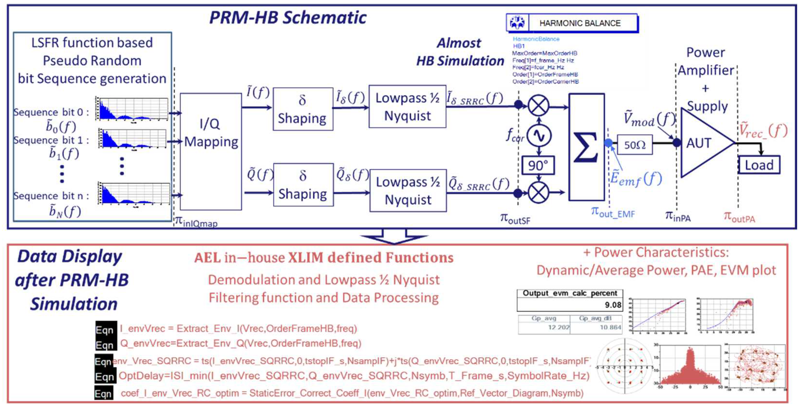
Figure 2.
Spectra in the 50 Ω load after PRM-HB simulation.
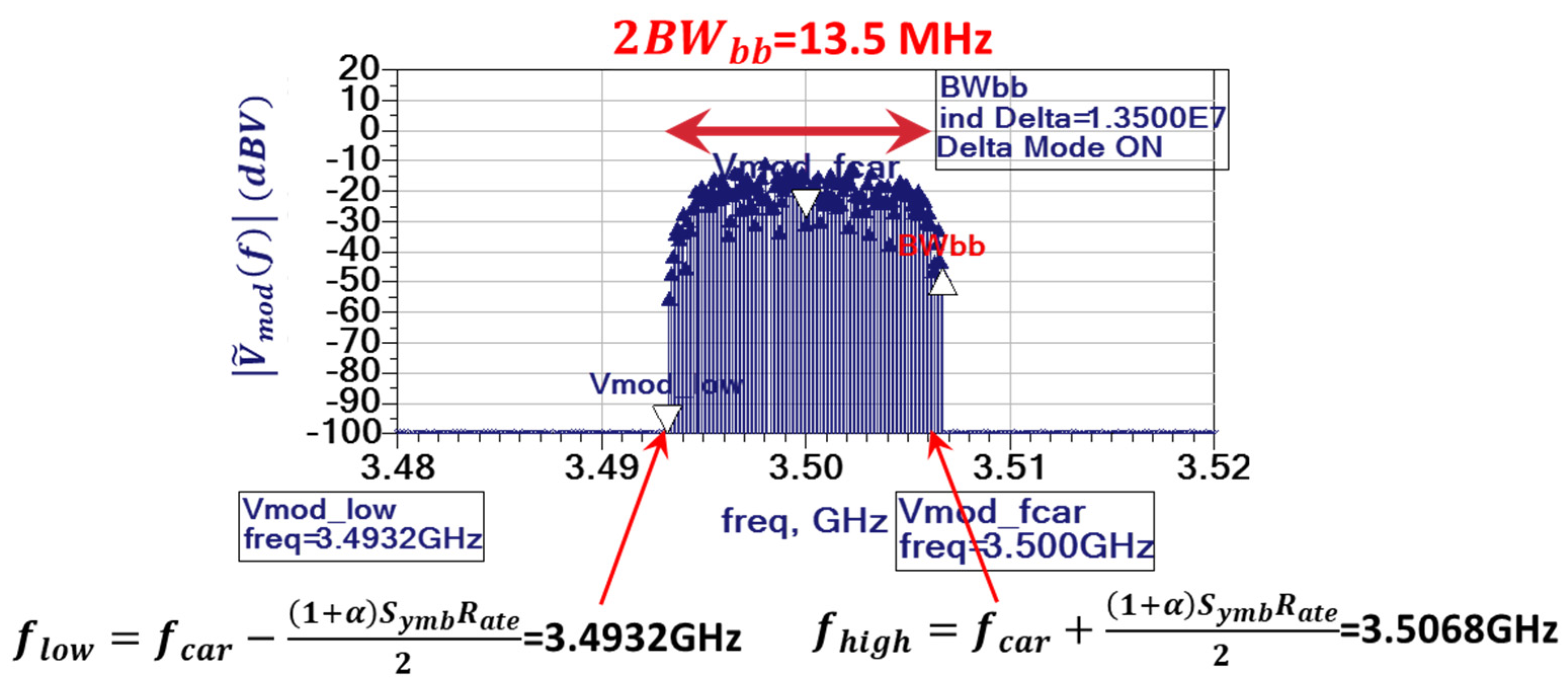
Figure 3.
Principle of the design flow graph of the demodulation and EVM calculation after PRM-HB simulation.
Figure 3.
Principle of the design flow graph of the demodulation and EVM calculation after PRM-HB simulation.
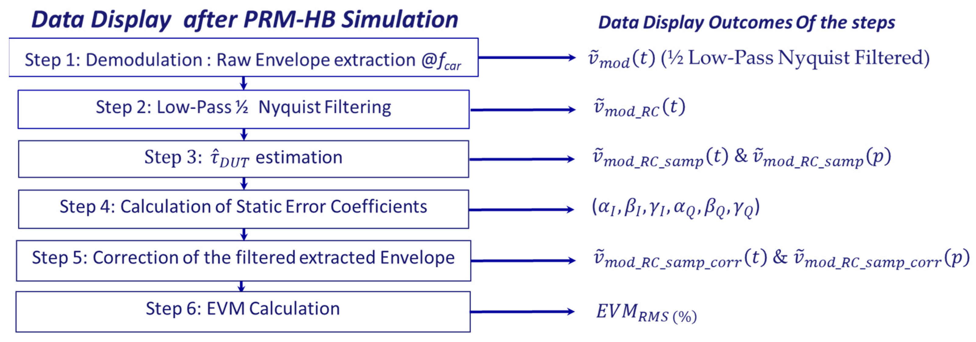
Figure 4.
Magnitude of the raw complex envelope, around , (dot) overlaid with the subsampled RF voltage (line).
Figure 4.
Magnitude of the raw complex envelope, around , (dot) overlaid with the subsampled RF voltage (line).
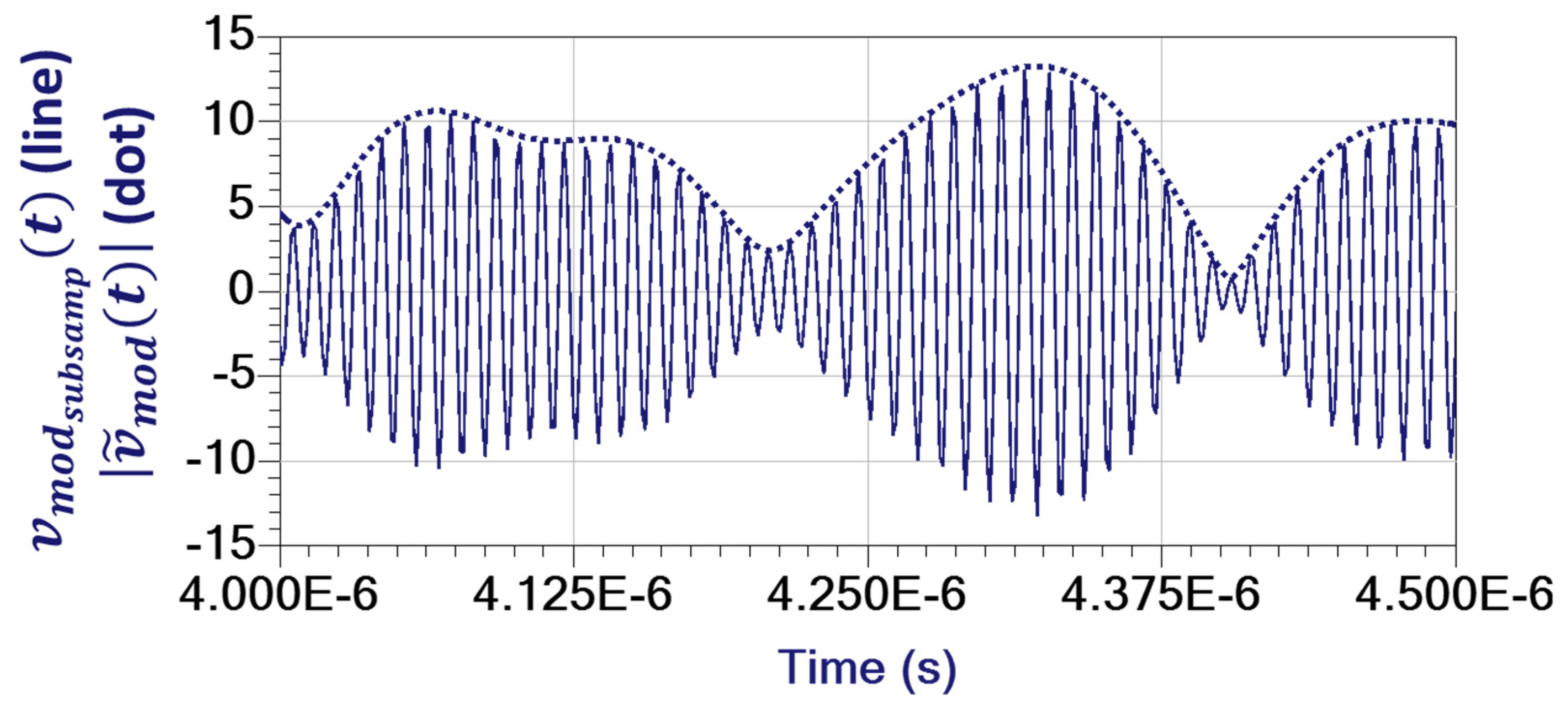
Figure 5.
Magnitude (zoom) of the raw voltage envelope (dot) overlaid with the RC filtered voltage envelope (line).
Figure 5.
Magnitude (zoom) of the raw voltage envelope (dot) overlaid with the RC filtered voltage envelope (line).
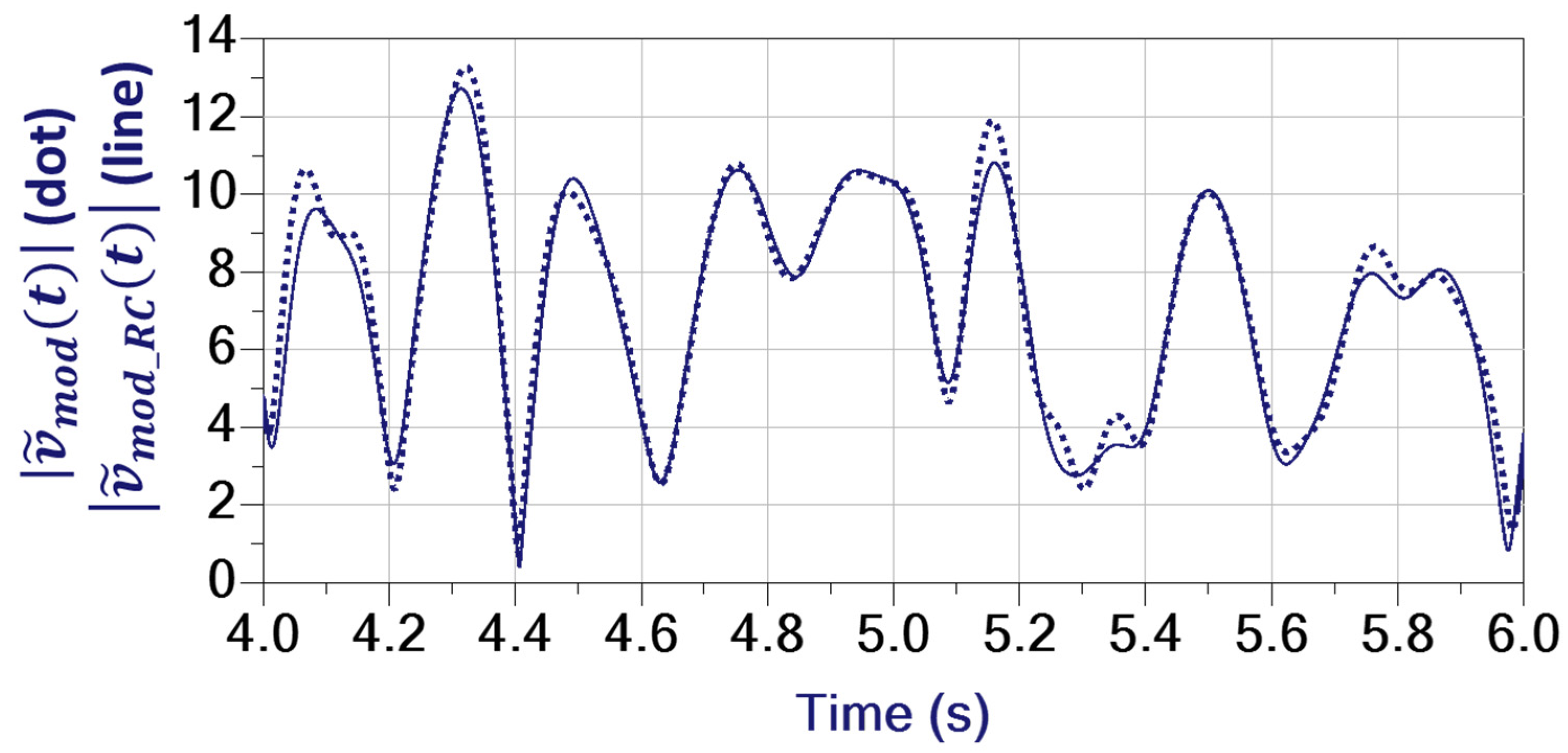
Figure 6.
Trajectories of the fully demodulated input voltage before optimal sampling (lines) and after optimal sampling (circles).
Figure 6.
Trajectories of the fully demodulated input voltage before optimal sampling (lines) and after optimal sampling (circles).
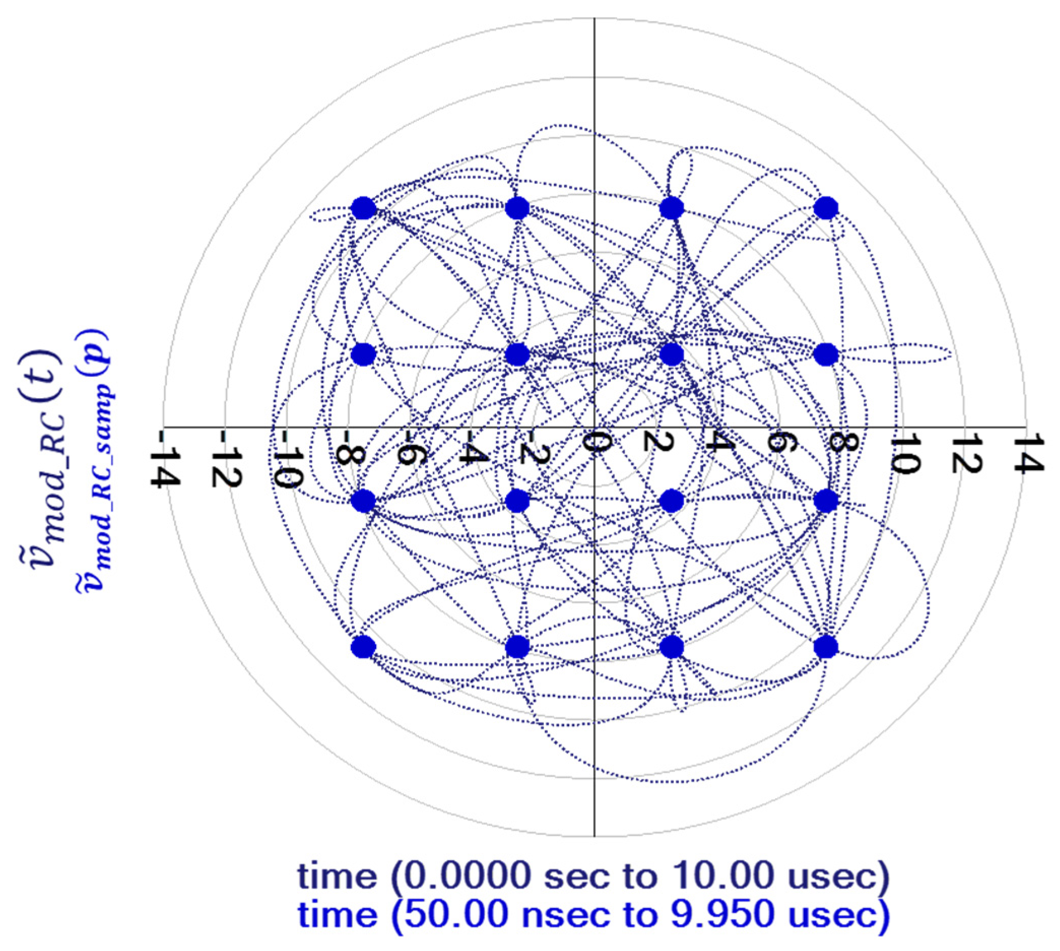
Figure 7.
(Zoom) of (green), with , (line) and (dot).
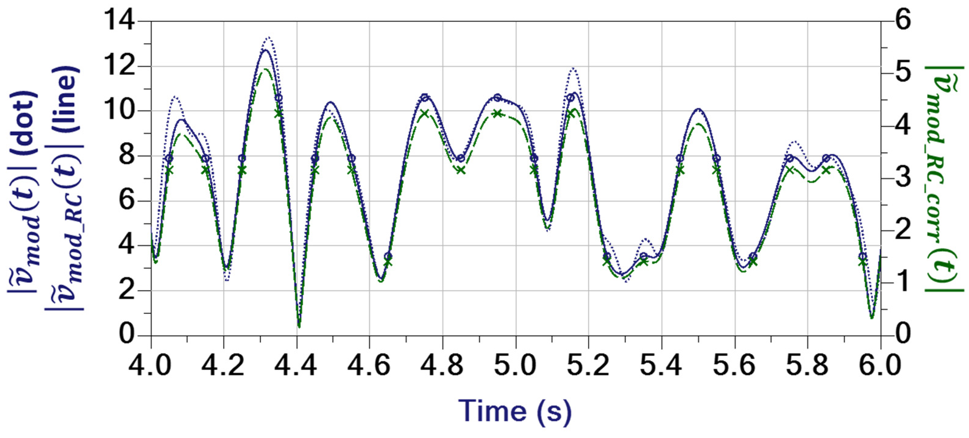
Figure 8.
Corrected 16-QAM Vector Diagram and 16-QAM Reference Vector Diagram.
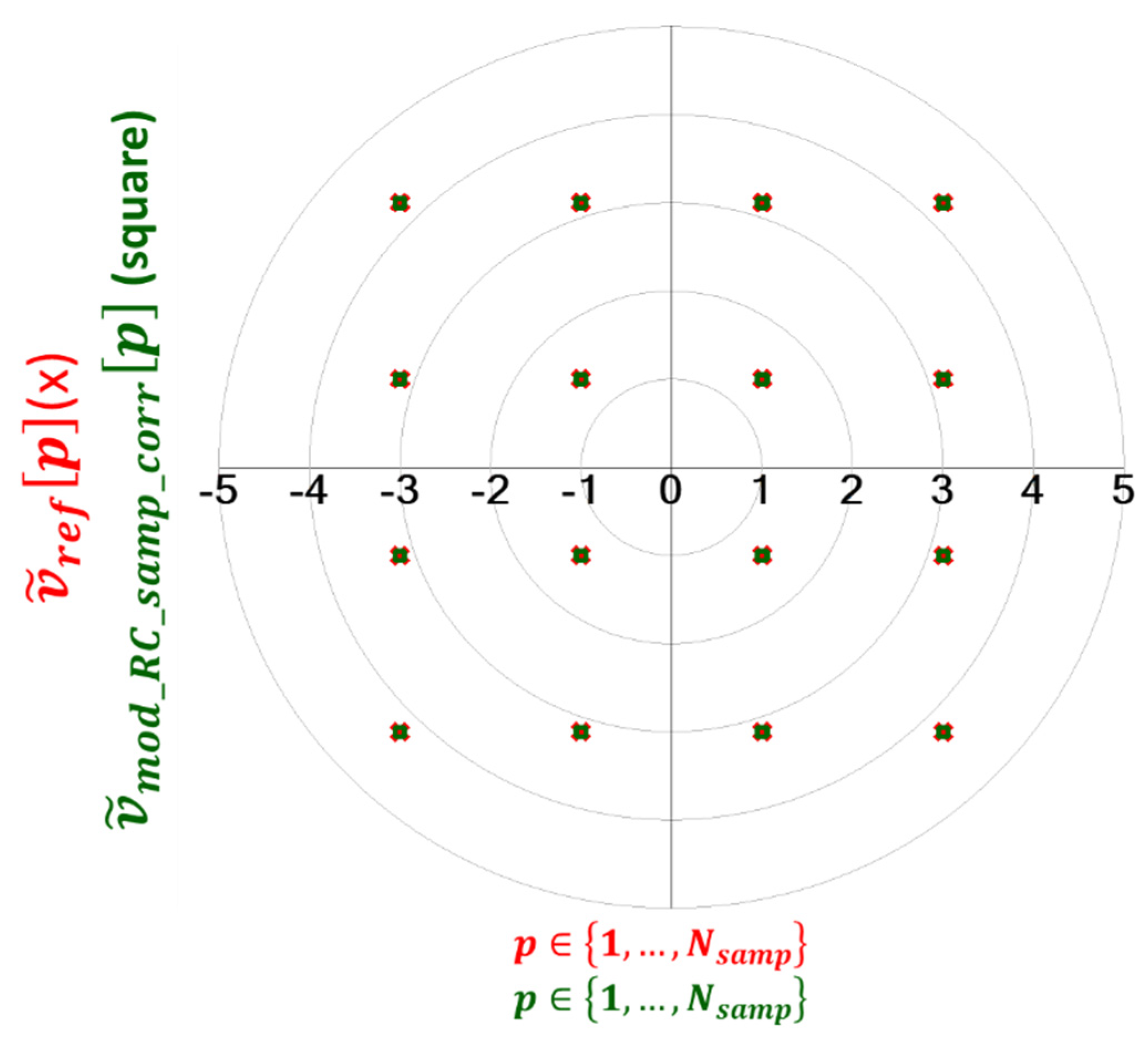
Figure 9.
Layout (a), Demonstration board (b) and Key Characteristics of the realized asymmetric packaged Quasi-MMIC SI-DPA [1].
Figure 9.
Layout (a), Demonstration board (b) and Key Characteristics of the realized asymmetric packaged Quasi-MMIC SI-DPA [1].
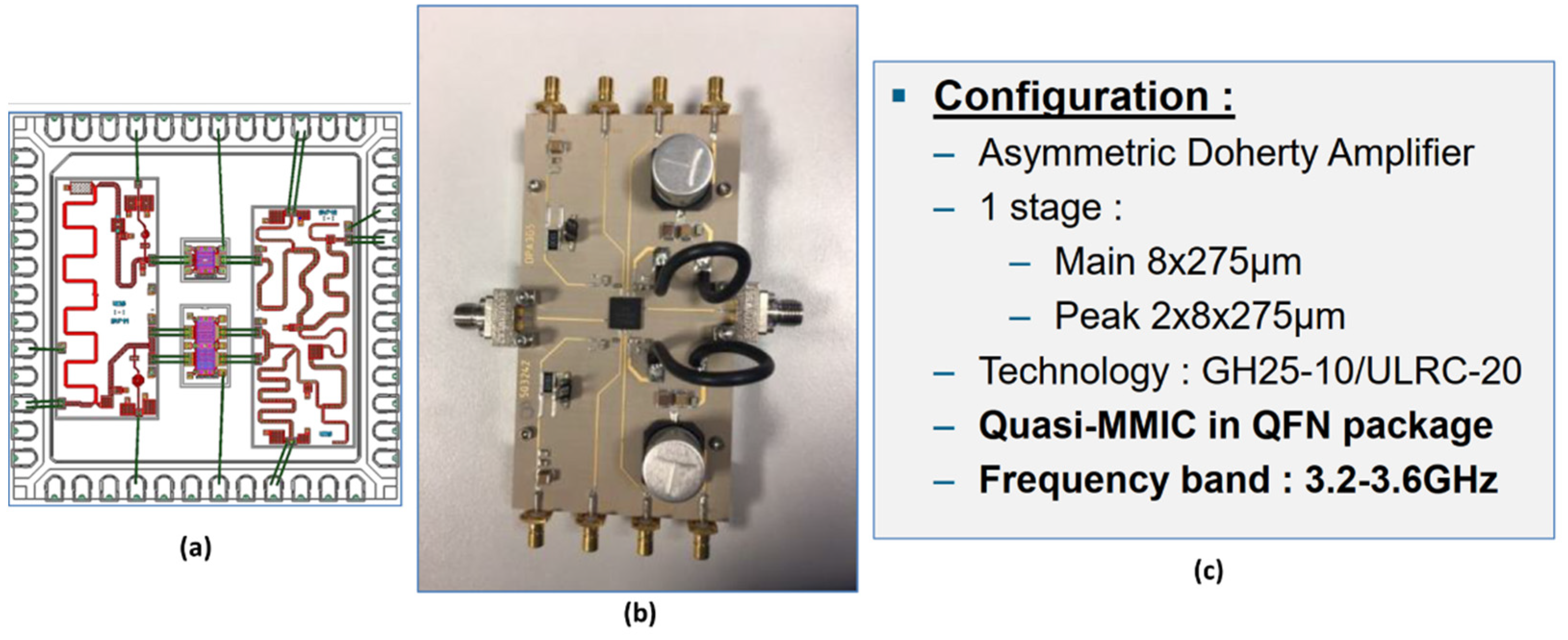
Figure 10.
Principle of Non-linear LAPTV Local Stability Analysis.
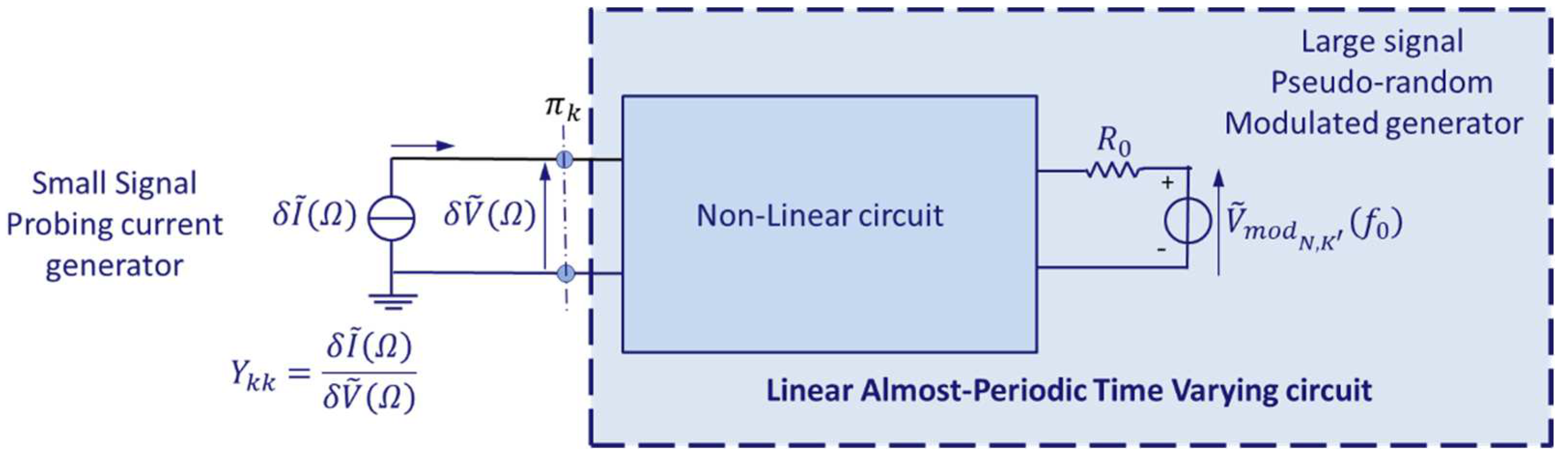
Figure 11.
Frequency sweep (Magenta colour) of the perturbating generator.
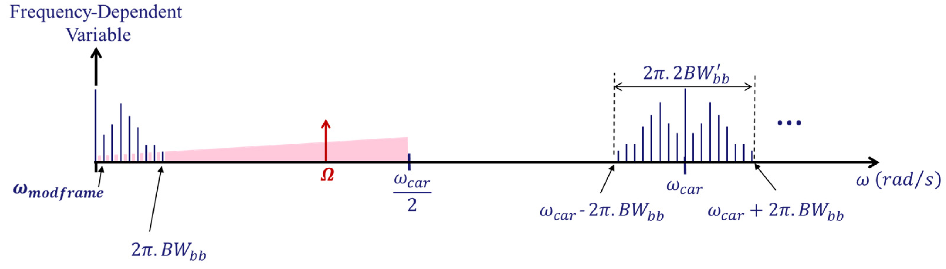
Figure 12.
Floquet exponents obtained from the STAN® software for the 3 chosen power levels in CW large signal regime.
Figure 12.
Floquet exponents obtained from the STAN® software for the 3 chosen power levels in CW large signal regime.
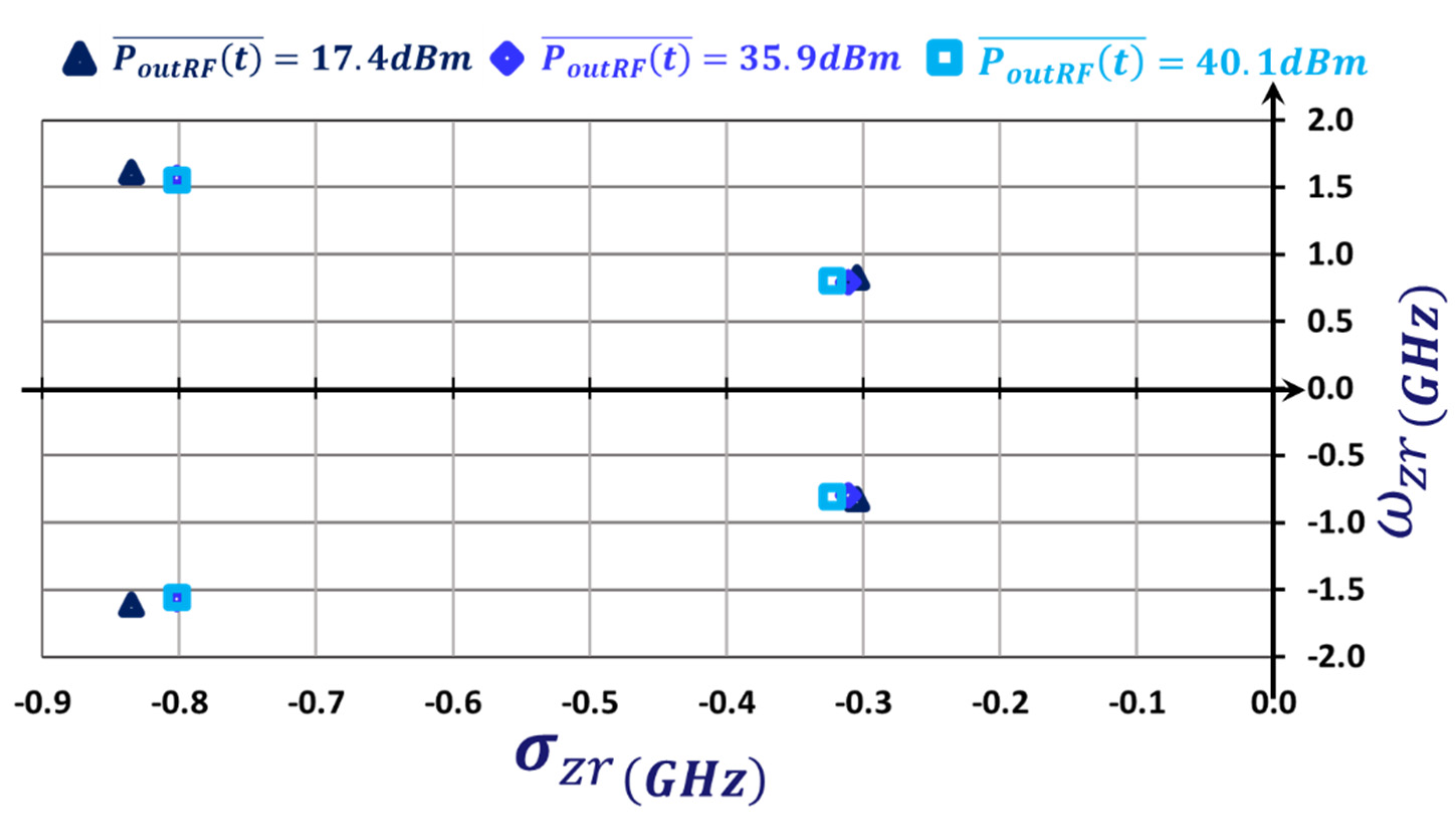
Figure 13.
Main results of the PRM-HB simulation of the DPA driven by CW and modulated 16-QAM EMF for .
Figure 13.
Main results of the PRM-HB simulation of the DPA driven by CW and modulated 16-QAM EMF for .
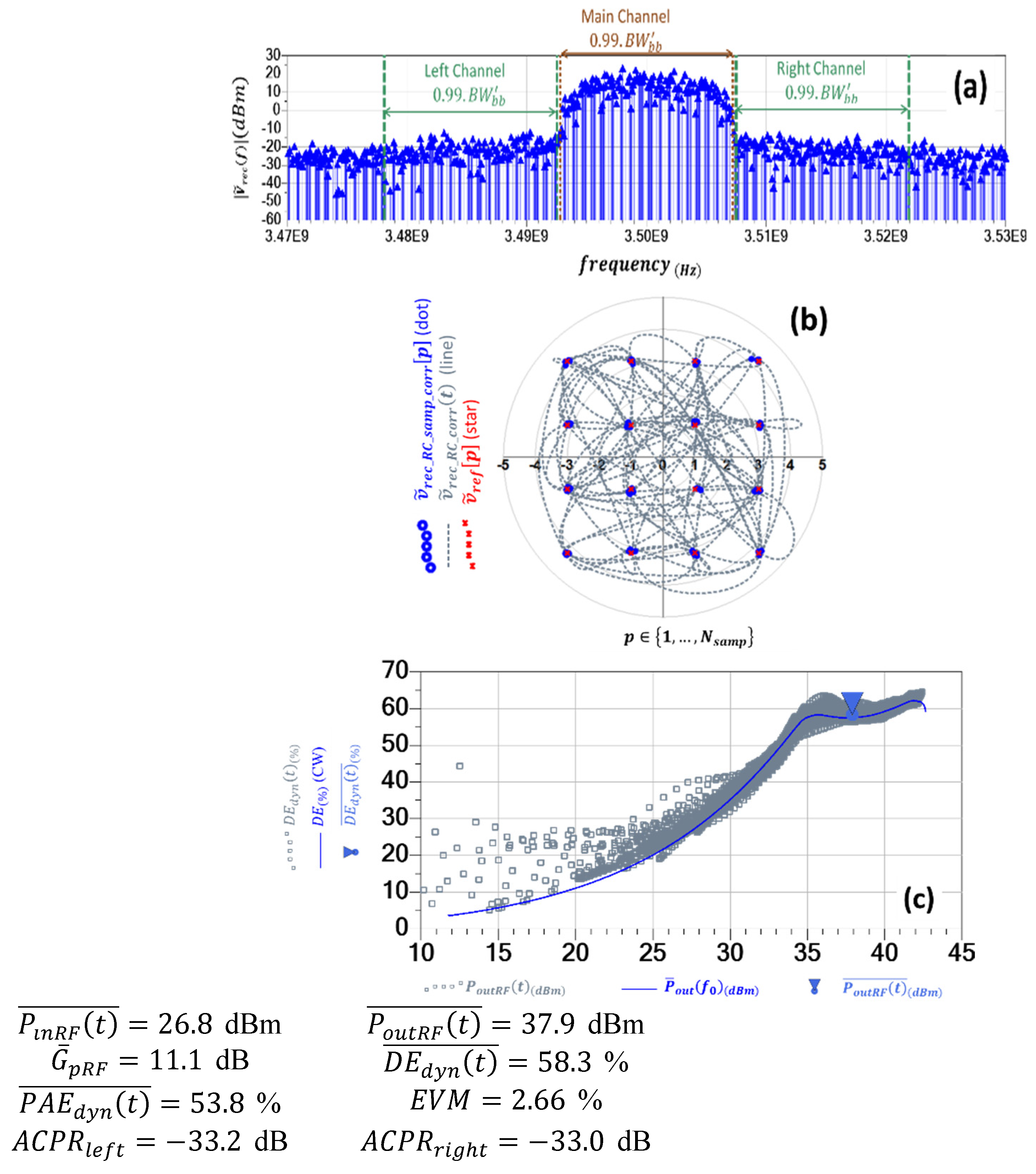
Figure 14.
6-channel time-domain measurement system for power measurements of non-linear devices, driven by the 10MS/s 16-QAM modulated voltage and injected in the plane.
Figure 14.
6-channel time-domain measurement system for power measurements of non-linear devices, driven by the 10MS/s 16-QAM modulated voltage and injected in the plane.
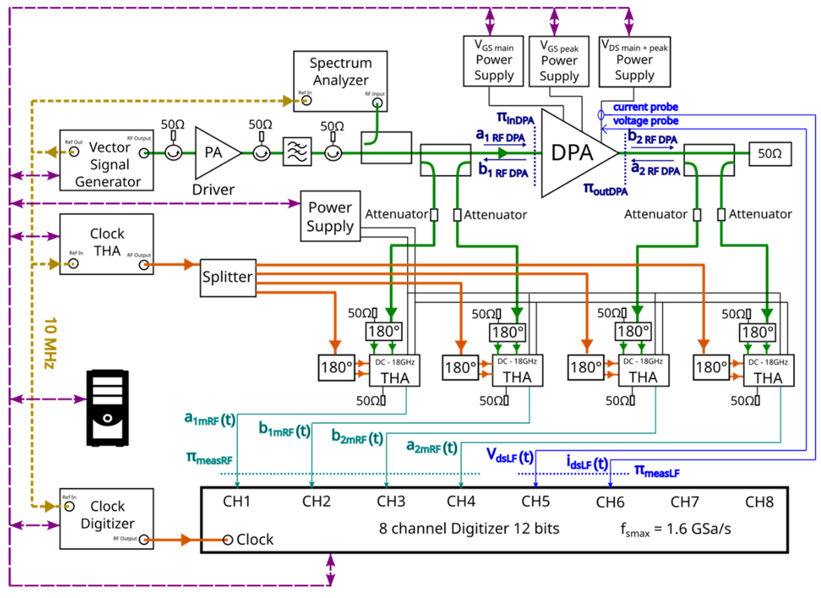
Figure 15.
Simulated and Measured Power performances of the DPA ( vs. ) driven with the 16-QAM 10 MS/s modulated voltage.
Figure 15.
Simulated and Measured Power performances of the DPA ( vs. ) driven with the 16-QAM 10 MS/s modulated voltage.
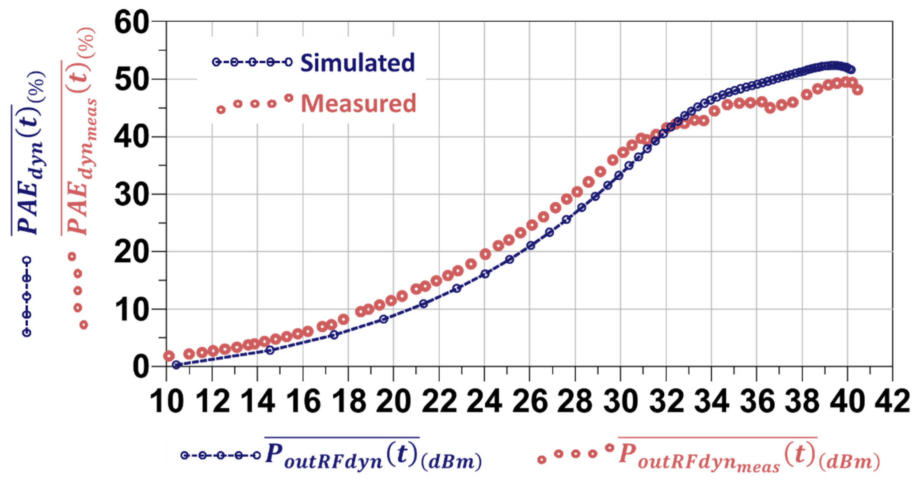
Figure 16.
Simulated and Measured Power performances of the DPA ( vs. ) driven with the 16-QAM 10 MS/s modulated voltage.
Figure 16.
Simulated and Measured Power performances of the DPA ( vs. ) driven with the 16-QAM 10 MS/s modulated voltage.
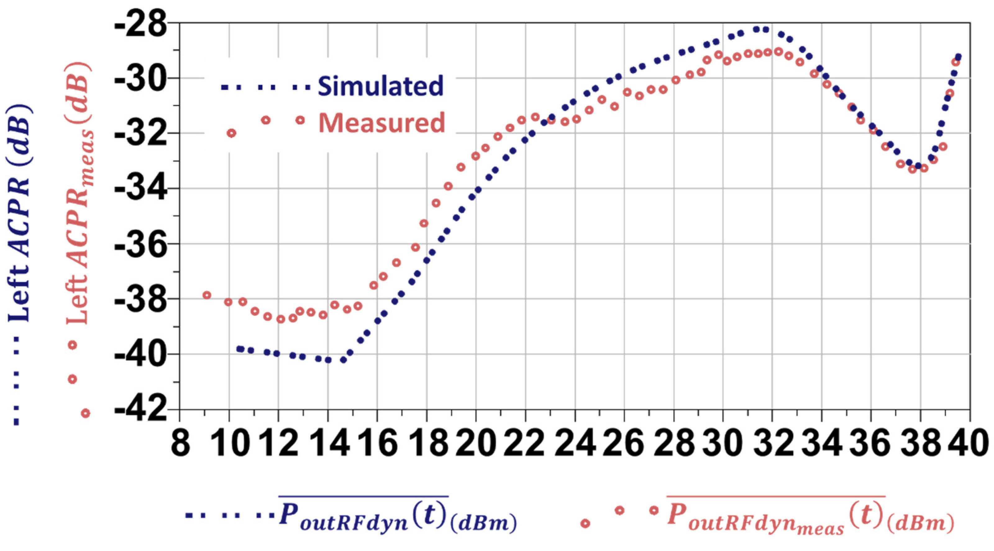
Figure 17.
Simulated and Measured Power performances of the DPA ( vs. ) driven with the 16-QAM 10 MS/s modulated voltage.
Figure 17.
Simulated and Measured Power performances of the DPA ( vs. ) driven with the 16-QAM 10 MS/s modulated voltage.
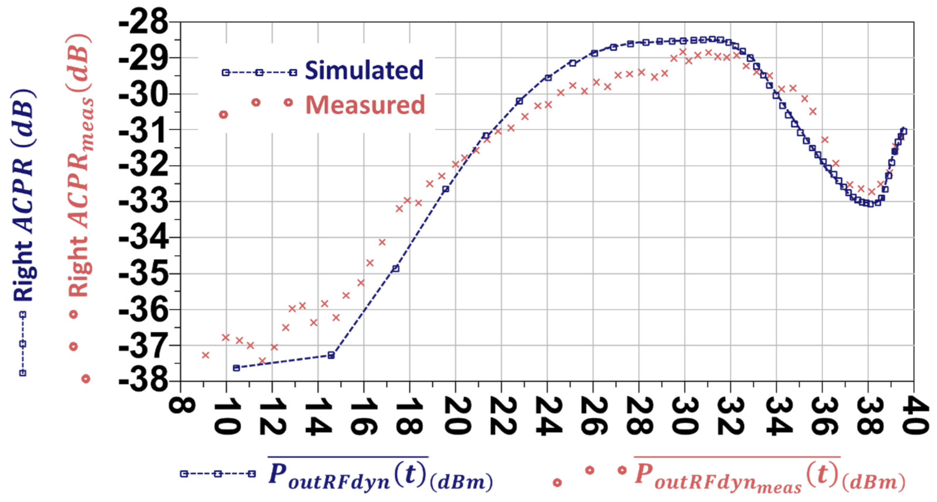
Figure 18.
Simulated and Measured Power performances of the DPA ( vs. ) driven with the 16-QAM 10 MS/s modulated voltage.
Figure 18.
Simulated and Measured Power performances of the DPA ( vs. ) driven with the 16-QAM 10 MS/s modulated voltage.
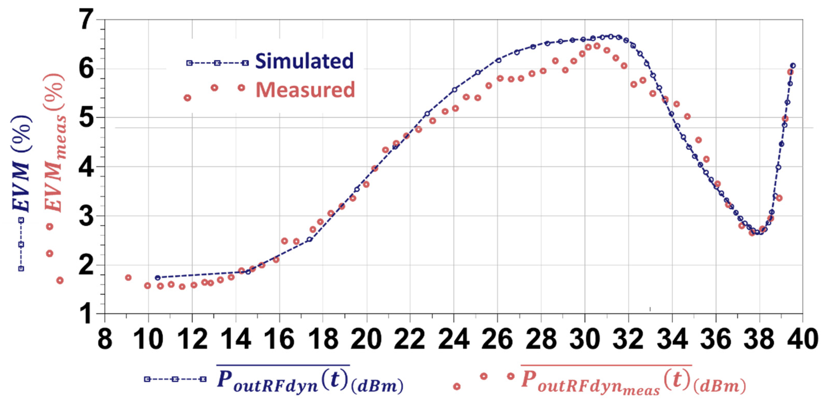

Table 1.
Parameters of the generated 16-QAM.
| Parameter | Value | unit |
|---|---|---|
| Symbol Rate | 10 | MHz |
| Symbol Number | 100 | |
| RollOff | 0.35 | |
| Harmonics of the periodic modulating signal | 500 | |
| Carrier Magnitude | 5 | V |
| Carrier Frequency | 3.5 | GHz |
| harmonics of the carrier frequency | 1 |
Table 2.
Parameters of the CW local stability simulation of the DPA.
| Parameter | Value with unit |
|---|---|
| Quiescent Main Voltage Drain | |
| Quiescent Main Voltage Gate | |
| Quiescent Peak Voltage Drain | |
| Quiescent Peak Voltage Gate | |
| CW Frequency | |
| CW Magnitude | (Step: 0.1V) |
| HB Order |
Table 3.
Additional parameters for the PRM-HB simulation of the DPA.
| Parameter | Value with unit |
|---|---|
| Quiescent Main Voltage Drain | |
| Quiescent Main Voltage Gate | |
| Quiescent Peak Voltage Drain | |
| Quiescent Peak Voltage Gate | |
| CW Frequency | |
| CW Magnitude | (Step: 0.1V) |
| HB Order |
Table 4.
Parameters for the 16QAM measurement of the DPA.
| Parameter | Value with unit |
|---|---|
| Carrier Frequency | |
| Carrier Power sweep | (Step: 0.5dB) |
Disclaimer/Publisher’s Note: The statements, opinions and data contained in all publications are solely those of the individual author(s) and contributor(s) and not of MDPI and/or the editor(s). MDPI and/or the editor(s) disclaim responsibility for any injury to people or property resulting from any ideas, methods, instructions or products referred to in the content. |
© 2024 by the authors. Licensee MDPI, Basel, Switzerland. This article is an open access article distributed under the terms and conditions of the Creative Commons Attribution (CC BY) license (http://creativecommons.org/licenses/by/4.0/).
Copyright: This open access article is published under a Creative Commons CC BY 4.0 license, which permit the free download, distribution, and reuse, provided that the author and preprint are cited in any reuse.


