Submitted:
14 December 2023
Posted:
14 December 2023
You are already at the latest version
Abstract
With the development of the photovoltaic industry, there will be an increasing demand for efficient, high-power density, and low-cost grid interface converters. Compared with two-level inverters, multilevel inverters have the following advantages: (1) lower device voltage ratings; (2) better output filtering spectrum; (3) lower electromagnetic interference (EMI) noise; and (4) higher switching speed capability. However, the complex switching circuit of the multilevel inverter will bring more parasitic inductance, resulting in more serious switching overvoltage (ringing). Consider that commonly used overvoltage absorption schemes are effective only for overvoltage or sup-pression of oscillations. Therefore, a new overvoltage absorption circuit is proposed in this paper, which can not only alleviate the overvoltage and ringing phenomena but also suppress the effect of voltage jumps during low-frequency switching on high-frequency input voltage. This overvoltage absorption circuit is characterized by low overvoltage, fast ringing damping, and minimum ca-pacitance. Experiments and simulations are conducted to verify the effectiveness of this overvoltage absorption circuit using a three-level ANPC inverter as a prototype. The results show that the proposed overvoltage absorption circuit can significantly reduce the overvoltage level, shorten the oscillation time, and reduce the voltage difference between the upper and lower DC bus capacitors.
Keywords:
multilevel inverter
; parasitic effects
; overvoltage
; ringing
; voltage jumps
1. Introduction
As the share of photovoltaic (PV) power generation in the electricity supply continues to grow, so does the demand for efficient, high-power density, lightweight, and low-cost converters. The development of the photovoltaic industry reduces the need for fuel for traditional thermal power generation, reduces carbon emissions, and makes an important contribution to the protection of the environment. Nowadays, the energy crisis is worsening, the development of traditional energy sources such as coal and oil has received resistance, and the promotion and popularization of new energy generation, smart grid technology, and electric vehicles [1] have led to the industry's need for a more stable, higher-power, and lower-loss power system. As an important part of the energy conversion system, the inverter is an important object of research in the power system, in which the three-level inverter receives more extensive attention.
Three-level inverters are undoubtedly the most popular choice for high-power and medium-voltage applications, offering lower EMI noise, lower voltage ratings on semiconductor power devices, better power quality, and more flexible control than conventional two-level inverters [2,3]. All the switches in a three-level ANPC inverter can be actively controlled, while different modulations can be applied to control the inverter [4,5] to achieve bidirectional power flow, thermal balance, and higher efficiency. Two commonly used modulation schemes are analyzed in detail in [5], where the parasitic inductance in the long loop modulation mode is significantly larger than that in the short loop modulation mode, the overvoltage in the long loop modulation mode is significantly higher than that in the short loop modulation mode due to the parasitic effect, and in the short loop modulation mode, the power switching devices have lower losses [6] and are subjected to lower stresses due to smaller parasitic inductance.
The efficiency of the inverter can be improved by using the hybrid modulation technique, a common three-level hybrid modulation technique, as shown in Table 1. In the first group (short loop commutation), the four switches in the first level are controlled by a high-frequency carrier, and the two switches in the second level are controlled by a low-frequency carrier. In the second group (long loop commutation), the four switches in the first stage are controlled by a low-frequency carrier, and the two switches in the second stage are controlled by a high-frequency carrier. However, under low-frequency switching, the second stage of the first group will introduce more switching losses. Although the parasitic inductance is significantly higher than that of the short-loop current-switching mode in the long-loop current-switching mode [7], the parasitic inductance in the circuit can be optimized by optimizing the PCB layout, thus reducing the parasitic inductance in the circuit and minimizing the parasitic inductance in the long-loop current-switching mode. At the same time, only two high-frequency switches are needed in the long-loop commutation mode, which is less costly compared to the short-loop commutation mode. Therefore, the three-level ANPC in long-loop modulation mode is considered the research object in this paper.
In the long loop current-switching mode, and synchronous switches, and synchronous switches, and and complementary switches, form a double-pole, double-throw switch as shown in Figure 1, with the red dashed line showing the direction of the current flow when and are on, and the blue dashed line showing the direction of the current flow when and are on, which results in a DC bus because there is only a single capacitor on the DC side used for charging or discharging. capacitor voltage imbalance. When switches and are switched to and , the input voltages of switches and will undergo large jumps, reducing the system characteristics.
The switching topology circuits applied in this paper contain wide bandgap (WBG) power semiconductor devices, which exhibit faster di/dt and dv/dt and provide higher voltage blocking capability, better thermal performance, and lower switching losses compared to Si IGBT [8,9]. However, the stability of wide-bandgap power semiconductors is affected by the parasitic inductance of the circuit, which can easily cause overvoltage [10] and voltage oscillations. In the three-level ANPC inverter, the commutation of wide-bandgap (WBG) devices [11] introduces multiple switching oscillation components, which will lead to overvoltage during switching transients. Also, the EMI performance will be affected by the different oscillation components. Layout-optimized DC bus design and control methods are proposed in [12,13], respectively, so as to reduce the overvoltage. From the switching state of a three-level ANPC inverter, it can be seen that each phase can output three different voltage levels, i.e., 、0、and -. When one of the phases is clamped to neutral, the neutral voltage becomes unbalanced due to the current flowing through it. Various PWM modulation schemes were proposed in [14-16] to minimize the voltage unbalance in the DC bus, but the approach improves the modulation difficulty of the converter system.
In order to analyze the effect of voltage jumps on high-frequency switching, the three-level ANPC hybrid modulation mode is used, which produces three levels per phase at the output. Due to the ANPC structure, in which the voltage across the switching device is half of the dc bus voltage, a switching device that is subjected to a lower voltage can be used. Considering the need to operate at high switching frequencies, GaN metal oxide power switching devices are used as high-frequency switches and Si MOSFETs as low-frequency switches in the three-level ANPC unit, and the long-loop hybrid modulation technique is used in this paper. Meanwhile, the effect of parasitic parameters on the performance of GaN metal oxide power switching devices requires the use of electromagnetic field finite element analysis to extract the parasitic parameters and design the overvoltage absorption circuit.
The rest of the paper is organized as follows: in Section II, common overvoltage (oscillation absorption) schemes are analyzed; in Section III, a new overvoltage absorption scheme is proposed; in Section IV, the application system design is elaborated, including parasitic parameter extraction and component parameter determination; in Section V, experimental simulations are performed; and finally, conclusions are given in Section VI.
2. Analysis of midpoint voltage unbalance mechanism
- A.
- Analysis of midpoint voltage imbalance
In the inverter operation, when the load side of one phase or two is connected to the neutral point of the DC bus, the current will flow from the neutral point O of the bus through the load to the neutral point N, which will make the DC bus capacitor constantly charging or discharging. If the capacitor's charging is not equal to the amount of its discharge, this process will lead to the neutral point O of the voltage shift. As shown in Figure 2a, it is assumed that the current flows from top to bottom through capacitors and capacitors , and the midpoint current is the direction of outflow from neutral O. It is also assumed that the direction of outflow from the neutral point is the positive direction of the current.
Then the voltage values of the capacitor and capacitor is:
The current flowing through capacitor and capacitor is:
Since the upper and lower capacitors have equal capacitance values and :
List Kirchhoff's current law for neutral O:
Further simplifying the above equation yields the change in midpoint voltage , △:
Ultimately, Eq. is the initial value of midpoint voltage, and the expression of midpoint voltage is obtained as:
When switches and are off and and are on, as shown in Figure 2b, the voltage source is switched from the original to , and the voltages of and are not the same due to the imbalance of the upper and lower capacitor voltages. When switches and are switched, the high-frequency switches and input voltages will be switched from to .
The simulation results show that the maximum capacitance voltage in the upper and lower parts reaches 414.5V and the minimum voltage reaches 385.9V as shown in Figure 3. Since the charging or discharging of the capacitor leads to a large capacitance current shockwave that causes fluctuations in the DC bus voltage, the mid-point voltage imbalance problem will bring a lot of hazards to the system, for example:
- (1)
- It will cause the voltage value of a DC bus capacitor to exceed a predetermined voltage value, and in serious cases, the DC bus capacitor will be damaged;
- (2)
- The power switching devices are unevenly loaded, which poses a greater challenge to the voltage resistance of the power switching devices;
- (3)
- The inverter output waveform contains low harmonics, which affect the output quality and reduce the power density.
- B.
- High-frequency switching input voltage jump analysis
For the GaN three-stage, three-phase ANPC inverter power stage design module (TIDA-010210), the output is a 380v three-phase voltage and the input is a DC-800V voltage. In the adopted long-loop current switching mode, the LF switch forms a double-knife double-throw switch, and the DC-side capacitors and are equivalent to the voltage source, which changes from to when the LF switch operates. Due to the unbalanced capacitor voltage on the DC side, it will cause the high-frequency switch to experience large voltage jumps during operation. When the inverter operates, the voltage of the upper capacitor will be higher due to the limited PWM modulation method and the unidirectional diode. The low-frequency switches form a double-knife, double-throw switch so that the high-frequency switch input voltage jumps from a high voltage to a low voltage. Figure 4a shows that when the low-frequency switching occurs when the high-frequency switch is subjected to the voltage from the maximum value of 414.5V suddenly dropping to the minimum value of 385.9V, the one-phase load current polarity also changes, as shown in Figure 4b. At this time, the three-phase load current is sinusoidally transformed, as shown in Figure 4c.
It is empirically known that the dc bus capacitance voltage difference will be affected by the inverter DC side capacitance and power, although the larger the dc side capacitance, the smaller the voltage difference. Considering the requirements for the size of the inverter as well as the cost, the dc side capacitance selection needs to be considered for practical applications. At a power (load) of 16 kW, the trend of the voltage difference with the size of capacitance is shown in Figure 5, and an empirical function is fitted, which shows that the rate of change of the voltage difference decreases gradually when the capacitance is larger than 300 μF.
The voltage jumps with power (load) at a DC capacitor size of 500 μF shown in Figure 6;
It can be seen that the voltage difference decreases exponentially as the capacitance becomes increases, while it is linear with the power (load) change. If a suitable method is not taken, when the low-frequency switch is switching, the larger voltage difference will cause the high-frequency switch to withstand a larger voltage stress, which will damage the high-frequency switch in more serious cases, and at the same time, the larger voltage will damage the capacitance, affecting the quality of the power output from the inverter and even preventing it from working normally. In this paper, in order to solve the hazards of voltage jumps on the inverter system, a method is proposed to make the input voltage of the high-frequency switch to maintain stability, and at the same time, it has a good absorption effect on the over-voltage (oscillation). A three-dimensional surface diagram is established by the effect of capacitance and power on the voltage difference, as shown in Figure 7. The voltage difference decreases exponentially with the increase of capacitance and increases with the increase of power (load). The DC bus capacitance size in the inverter used in this paper is 500μF. and the power is 16 kW. The measured voltage difference is 29 V, which is consistent with the data on the fitted three-dimensional surface.
3. Overvoltage (oscillation) absorption program design
Oscillations occur between the parasitic inductance in the power circuit and the parasitic capacitance of the switching device in both on and off transients, and oscillations are unavoidable. In high-speed switching, ringing occurs due to sharp fluctuations in voltage and current during switching. Ringing leads to electromagnetic interference (EMI) noise and faults, which threaten system reliability. Therefore, it is necessary to solve the ringing noise problem, especially for MHz switching [17]. Due to the complexity of the three-level ANPC structure [18-20], more parasitic inductance is introduced into the circuit, which can easily lead to overvoltage in the switching devices. To suppress the switching oscillations, methods including optimizing the PCB layout, gate driving, adding oxide beads, and adding buffer circuits have been proposed. Since the parasitic parameters have a great influence on the parasitic oscillations, high-frequency paths should be established to take the parasitic parameters into account when designing the buffers. Optimizing the PCB layout can only reduce the parasitic parameters to a limited extent. Gate drive can reduce the switching oscillations by controlling dv/dt and di/dt, but it increases the complexity of the driver circuit and the difficulty of the circuit design. High-frequency noise can be suppressed by adding oxide beads; however, the oxide beads will introduce additional losses and the damping performance will deteriorate under high current conditions due to magnetic saturation. Through research in recent years, a variety of buffer circuits have been designed to suppress overvoltage and oscillations with good suppression effects, and the mainstream buffer circuits will be analyzed and compared in the following.
The RC snubber circuit consists of resistor and capacitor . The RC snubber circuit slows down the switching speed by dragging out the switching time and slowing down the switching speed. Thus, can cause to be completely discharged during the switching time period. In addition, can cause the voltage to rise at a slower rate and extend the oscillation period, which can reduce the switching loss and overvoltage. RC snubber has excellent suppression of switching oscillation performance and limited overvoltage suppression performance and is highly regarded, and at the same time, RC snubber has almost no negative impact on the switching loss of the switching device. However, the snubber dissipation is inevitable in itself, and the RC snubber loss is reduced as the snubber capacitance decreases or the snubber resistance increases [21]. Especially in the fields of high voltage, high current, and high frequency, RC snubber circuits generate additional thermal effects, and this loss will increase the difficulty of heat dissipation in the inverter. It is demonstrated in [22] that the RC snubber is not very suitable for high-frequency and high-speed applications because the snubber resistor increases the absorption time of the snubber circuit and slows down the absorption speed of the snubber circuit.
While Joko et al [23] proposed a combined C-RC snubber circuit where a single capacitor branch is responsible for absorbing overvoltage spikes and the RC branch is used to damp switching oscillations, it was shown that the C-RC snubber can overcome low-frequency oscillations, and it was demonstrated in [24] that the performance of suppressing the overvoltage can be significantly improved by increasing the values of and in the RC snubber, which is This is because the capacitance limits the severe voltage fluctuation of the bridge arm, but the DC bus capacitance voltage difference decreases slower and slower as the values of and increase, so it is not necessary to select larger capacitance ( and ) to slightly increase the suppression effect; otherwise, it will have adverse effects, e.g., additional parasites and a larger size of the inverter. It is shown that when and are kept constant, the increase of will weaken the suppression performance, and when and are kept constant, the decrease of does not have a great impact on the overvoltage suppression effect. Although the C-RC snubber circuit can realize an excellent overvoltage suppression effect compared with the traditional RC snubber circuit, its performance in suppressing turn-off overvoltage is still unsatisfactory. Theoretically, the power loss of C-RC snubber circuits is lower than that of RC snubber circuits, which is very beneficial in high-power, high-frequency areas.
[25] propose an RC-D snubber circuit that evaluates the effect of wiring inductance on switching device switching, discusses the mechanism of ringing caused by wiring inductance, and suppresses ringing by an RC-D snubber circuit that takes into account the location of the wiring inductance. When the parasitic inductance is mainly concentrated at the source of the switching device, the RC-D snubber cannot suppress ringing, and the drain-source voltage oscillation will be more severe. The RC-D snubber circuits have excellent performance for suppressing the switch drain-source voltage ringing when the parasitic inductance is concentrated at either the switch gate or drain. However, the RC-D snubber circuits are not sufficient when the parasitic inductance is mainly concentrated at the switch gate to suppress switch drain-source voltage ringing and may cause malfunction or breakdown. Considering the location of the wiring inductance, the wires near the gate and source should be reduced as much as possible when optimizing the design of the RC-D snubber, and the parasitic inductance near the gate and drain terminals must be taken into account, while the RC-D snubber circuit does not have a significant effect on the reduction of the switch drain-source inter-voltage oscillation.
By analyzing the previous research ideas, most of them use a one-way absorption circuit to achieve the purpose of reducing the switch-off overvoltage or suppressing the oscillation. On this basis, it is proposed to hypothesize whether it is possible to reduce the switch-off overvoltage and suppress the voltage oscillation if another release circuit is added on top of the one-way absorption circuit. Therefore, in this paper, an overvoltage absorption circuit (RC-CD) is proposed, which is connected in parallel between the first and second stages as shown in Fig.8(a). Under different PWM strategies, the two input capacitor ( and ) voltages are always unbalanced because only one capacitor is used for charging or discharging, and the unbalance of the input voltage increases the output voltage waveform. Therefore, in order to minimize the effect of the input capacitor voltage imbalance on the system characteristics, the voltage of the absorbing capacitor is kept slightly above half of the DC voltage and maintained in a steady state by adding a voltage regulator diode to the release circuit. When the constituted double-knife double-throw switches , and , are switched at low frequency, the input voltages of the high-frequency switches and do not jump when low-frequency switching occurs due to the parallel connection of capacitance with the high-frequency switching input capacitance while the RC-CD circuit is placed between the low-frequency stage and the high-frequency stage, which splits the large commutated circuit into two smaller circuits and is proposed to be the three-level ANPC structure used in the experiment.
When and are on, the equivalent circuit of this overvoltage (oscillation) absorption circuit is shown in Figure 8b, with as the equivalent circuit voltage source, as the parasitic capacitance on the drain-source stage of the high-frequency switch or , and , , and as the circuit parasitic inductors. Ideally, the voltage of the absorption capacitor is equal to half of the DC bus voltage, so the voltage difference between and is smaller, resulting in a smaller current flowing through the main circuit parasitic inductor ; in other words, the smaller the energy stored in the main circuit parasitic inductor , When the low-frequency switching is switched, the RC-CD circuit suppresses the jump in the high-frequency switching input voltage caused by the DC bus capacitor voltage imbalance, thus improving the stability of system operation.
When the input current is positive, the current flows through the diode () and resistor () to and , respectively, and the energy stored in the parasitic inductors will charge capacitors and , which will reduce the energy flowing into the high-frequency switching input capacitor , thus reducing the high-frequency switching overvoltage. When the voltage on and is higher than , the voltage difference starts to drive a negative current, but the negative current will not flow directly into , but through resistor , and the energy will be consumed through resistor , thus reducing the voltage oscillations on the high-frequency switch.
This overvoltage absorption circuit effectively reduces the switching device turn-off overvoltage while oscillation suppressing the oscillation. At the same time, due to the addition of a high voltage capacitor , the input voltage jump on the high-frequency switch can be suppressed during low-frequency switching. During system operation, if the voltages on the DC bus capacitors and are 415 V and 385 V, respectively, and the voltage of the high voltage capacitor is 400 V, When and are on, and serves as the voltage source of the circuit (415 V), as shown in Figure 9a, the capacitor voltage is lower than that of , and due to the reduction in the voltage difference, the energy stored in the parasitic inductance is reduced. The energy charged to and through the diode () and the resistor () will be reduced, and due to the small junction capacitance of the diode () in the CD loop, it will cause the circuit to have a high-frequency oscillation, but due to the addition of the RC loop, the energy stored in the parasitic inductance can be absorbed on the one hand, and on the other hand, it can inhibit the high-frequency oscillation caused by the junction capacitance of the diode (). When the capacitance voltages of and are higher than , the energy stored in and will be consumed by resistor , as shown in Figure 9b, thus reducing the low-frequency oscillation on the high-frequency switch. When the low-frequency switch switches, and turn off, and conduct, is less than the capacitor voltage, the parasitic inductor is energized, and the high-frequency switch input voltage jump will be effectively suppressed because the absorption capacitor is kept at a high voltage level, as shown in Figure 9c. When the voltage is higher than the capacitor voltage, the stored energy of the parasitic inductor will energize and through the diode () and the resistor (), as shown in Figure 9d.
In this paper, the hybrid modulation strategy in the long loop mode is adopted, which results in a larger loop parasitic inductance. Although a larger loop parasitic inductance increases the switching device turn-off voltage, a larger loop parasitic inductance can reduce the switch on-state voltage and improve the switching response speed. Assuming that the main circuit parasitic inductance and the branch circuit parasitic inductance are the same, the inductors and store the same amount of energy, and when the switch turns on, the energy stored in will be released to the high-frequency switch, resulting in too high a voltage at the time of the high-frequency switch turn-on, and the overvoltage absorber circuit (RC) has to be used to lower the on-state voltage. However, when the parasitic inductor in the main circuit is much higher than the branch parasitic inductor , the inductor will store a large amount of energy, while the energy stored in will be very limited. When the switch is on, the energy stored in the parasitic inductor will be absorbed only on the DC side of the high-frequency half-bridge, and there is no need for an additional over-voltage absorber circuit. and The high-frequency switch on-conducting voltage will be suppressed very well without causing damage to the switch.
The conclusion is drawn from the simulation experiment, which is consistent with the analysis results. As shown in Figure 10, when the parasitic inductance is low, the power device on-current curve is the red curve in the figure. When the parasitic inductance is high, the power device on-current curve is the yellow curve in the figure. In the low parasitic inductance circuit, add the RC damping circuit; its on-current curve is the blue curve. It can be seen that when the loop parasitic inductance is high, there is no need to introduce an additional RC damping circuit, and at the same time, the higher parasitic inductance helps to optimize the power device on-state characteristics and reduce the power device on-state loss.
4. Application system design
- A.
- Parasitic parameter extraction
In the three-level ANPC, due to the complexity of the device, and this paper chooses the long loop modulation method as the object of this study, it is inevitable to introduce more parasitic inductance and parasitic resistance; however, the parasitic parameters play a key role in the voltage overshoot of the switching device. Therefore, in the process of circuit simulation, it is very necessary to consider the parasitic parameters. about The extraction of parasitic parameters in the previous study did not mention that in the inverter work, the frequency will also have an impact on the parasitic parameters. This paper through the establishment of an electromagnetic field simulation model and electromagnetic field finite element analysis.
Parasitic inductance and parasitic resistance are the main parasitic parameters, in the previous study, although the parasitic parameters are mentioned, the source of parasitic parameters is not analyzed, in [4] it is mentioned that the parasitic parameters of switching devices are introduced according to the datasheets, in the actual circuit, especially the current converter circuits in the three-level ANPC inverter system are complex, the data obtained from the datasheets differ from the actual circuit parasitic parameters, and this difference will lead to changes in the switching characteristics, in this paper, the magnetic field finite element analysis of the circuit is carried out by using electromagnetic field simulation software to obtain the parasitic parameters between the nodes of the circuit at a frequency of 100kHz, and to establish the electromagnetic field simulation model of the corresponding circuit, as shown in Figure 11, where the copper curve replaces the capacitance in the established simulation model, where the green dashed box is the switching module, the blue color represents switching conduction, and the gray color represents switching off. Where A, B, and C correspond to the O, P, and N states of the circuit, respectively, and the desired parasitic parameters can be measured by measuring the nodes between A-3, 2-5, B-1, 4-7, and 6-C.
- B.
- Parameter selection
Suitable component parameters allow the damping circuit to be utilized to greater advantage, reducing overvoltage while suppressing oscillations. By analyzing the trend of overvoltage and oscillation with the variation of damping parameters, the preliminary component parameters can be derived. Through the parameter scanning, it is learned that capacitor has a greater impact on the switch-off overvoltage; as shown in Figure 12, the maximum voltage on the switching device decreases with the increase of capacitance . After the capacitance value of is larger than 25nF, the overvoltage absorption is not ideal, and it will also increase the size of the inverter and reduce the power density. Smaller capacitance values also do not have the effect of absorbing the overvoltage. In summary, the optimal parameter for capacitor is 25nF, and using the same methodology, the values of , , and will also be determined (=4nF, =25nF, =350Ω, and =40Ω).
.
5. Experimental results
- A.
- Experimental preparation
In this paper, a new overvoltage absorption scheme is proposed, as shown in Figure 10, which is used to suppress the overvoltage and oscillation of the switching devices during inverter operation. The setup hardware is a GaN-based three-phase ANPC inverter power stage design module (TIDA-010210) using two GaN HEMT modules on the DC side of the inverter (、 and 、), a Si MOSFET module connected in parallel on the AC side of the inverter ( and ), and an 800V DC voltage provided on the DC bus, which theoretically In theory, the two capacitors ( and ) on the DC side will be subjected to 400V. At the same time, this power design module uses a short-loop modulation scheme. During the operating phase, the value of the parasitic inductance in the circuit is much smaller than that of the long-loop modulation scheme, and the energy stored in the parasitic inductance is smaller, resulting in a smaller switch-off overvoltage, so the original scheme adopts a simpler overvoltage absorption circuit. However, in order to reduce the cost of the inverter, the article proposes a scheme that uses a long loop modulation scheme instead of the original scheme, where two Si MOSFET modules are used on the DC side of the inverter (、 and 、), and one GaN HEMT module is connected in parallel on the AC side of the inverter ( and ). The long loop modulation scheme involves longer operating loops and more switching devices, which will lead to a larger parasitic inductance in the circuit, which in turn will substantially increase the switch-off overvoltage. and the original overvoltage absorber circuit is obviously no longer able to satisfy the demand, and new overvoltage absorber circuits need to be designed in order to reduce the switch-off overvoltage. The specific parasitic inductance value can be measured from Section 4, which is a process of visualizing the parasitic inductance and intuitively perceiving that the parasitic inductance in the long loop is much larger than that in the short loop.
For the high switching frequency of the 100 kHz inverter used, a second modulation method is applied to the three-level ANPC unit in order to reduce the total switching losses of the three-level ANPC and to improve the efficiency. The proposed switching pattern is shown in Figure 13. The switching pattern of the three-level ANPC unit is a decoupled two-stage low-frequency and high-frequency modulation scheme. The LF (, ) and (, ) switching signals are generated by the over-zero detector as follows:
Therefore, the LF (, ) and (, ) switches operate at the fundamental frequency.
To generate the high-frequency (, ) switching signals, the modified reference voltage is defined as:
The proposed switching pattern for each phase ANPC is shown in Figure 14, where the high-frequency triangular carrier signal of one phase is phase-shifted by 2π/3 radians to generate a high-frequency switching signal for each three-level ANPC branch. The high-frequency signals are made to commutate only at 100 kHz to meet the desired requirements of the device. At the same time, each phase generates a 3-level output voltage. Thus, the number of output line-line voltage levels is 7, which makes the three-phase inverter have high power quality, and the load current is uniformly distributed in each branch of the three-level ANPC.
- B.
- Test results
From the experimental results, it can be seen that when no program is used to deal with the DC bus capacitor voltage, as shown in Figure 15a, the charging and discharging frequencies of the upper and lower capacitors are too high, and the voltage float is large. In low-frequency current exchange, the large voltage difference will cause a large current impact on the high-frequency switching device, which will damage the high-frequency switching device in serious cases. After using the overvoltage absorption circuit proposed in this paper, the DC bus capacitor voltage is shown in Figure 15b, the upper and lower capacitor charging and discharging frequencies are reduced, and at the same time, the voltage fluctuation is small, which will prolong the service life of the capacitor and improve the reliability of the inverter. In the event of low-frequency current switching, this circuit will reduce the current shock received by the high-frequency switch.
Based on the optimum component parameters obtained in Section IV, the optimum switching voltage waveform is obtained as shown in Figure 16. The maximum voltage is 400.5V, and the oscillations are well suppressed.
6. Discussions
In this paper, a new overvoltage absorption circuit is proposed that is distinguished from the traditional overvoltage absorption circuit and realizes the functions of reducing overvoltage and suppressing oscillation at the same time. Traditional overvoltage absorber circuits (e.g., RC, C-RC, and R-CD) have a significant effect on reducing overvoltage or suppressing oscillations; however, with the increase in switching device operating frequency and operating voltage, the traditional overvoltage absorber circuits cannot meet the demand of inverters better. In order to reduce the switching loss and improve the efficiency of the inverter, this paper proposes an optimization of the overvoltage absorption circuit, which has two main circuits, absorbing the overvoltage on the one hand and releasing the overvoltage on the other. The main idea is that when the high-frequency switch is turned off, the absorption circuit absorbs the power stored in the parasitic inductor to reduce the switch-off overvoltage. Then, the release circuit feeds the stored power back into the DC bus capacitor through a diode. This has the advantage of releasing this excess power to the DC bus capacitor instead of charging and discharging it between the switching output capacitor and the capacitor in the overvoltage absorption circuit. On the other hand, the voltage of the upper and lower DC bus capacitors can be balanced by the release circuit to reduce the current impact on the high-frequency switch due to the voltage imbalance of the DC bus capacitors during low-frequency current conversion.
In this paper, a hybrid modulation strategy is also used, and the long-loop hybrid modulation mode is very suitable for the study due to the consideration of cost as well as efficiency. The cost and efficiency of the hybrid modulation mode are studied in detail in [26-28], where a large number of studies have proved that the hybrid modulation mode is undoubtedly the best solution to reduce the cost of the inverter, and the cost can be reduced by nearly half in the hybrid modulation mode of Si and SiC.
Although the cost can be reduced by using hybrid modulation mode, more parasitic inductance is introduced in the long loop mode, which is detrimental to the reduction of the switch-off overvoltage and requires a redesign to optimize the overvoltage absorption circuit. While investigating the effect of high parasitic inductance on overvoltage, we find that higher parasitic inductance is beneficial for reducing the on-state current and also reduces the switch on-time, which can be further investigated for the effect of high parasitic inductance on the switch on-state loss. This phenomenon is slightly shown in Figure 10 of this paper, and it can be seen that high parasitic inductance significantly reduces the peak current during switch on-time compared with low parasitic inductance, and the oscillation time is shorter.
In future research, it can be demonstrated experimentally that the value of parasitic inductance will balance the switch-off overvoltage and the switch conduction current, which will provide supporting data for further optimization of the overvoltage absorption circuit, thus reducing the switch-off loss and conduction loss and improving the efficiency of the inverter.
7. Conclusion
In this paper, a new overvoltage absorption circuit based on the three-level ANPC hybrid modulation mode is presented, and the advantages of this overvoltage absorption circuit include:
- (1)
- Lower cost because the number of GaN power switching devices is smaller using the long-loop hybrid modulation technique.
- (2)
- Smaller capacitance values are used, allowing the inverter to have a smaller size and increased power density.
- (2)
- The capacitor voltage in this overvoltage absorption circuit is slightly higher than the theoretical DC bus capacitor voltage, which does not cause high-frequency switching input voltage jumps during low-frequency switching.
Author Contributions
Conceptualization, J.Y. and R.S.; methodology, J.Y.; software, R.S.; validation, R.S.; formal analysis, L.Z.; investigation, Z.J.; resources, Y.H; data curation, R.S.; writing—original draft preparation, R.S.; writing—review and editing, J.Y.; visualization, R.S.; supervision, J.Y.; project administration, J.Y. All authors have read and agreed to the published version of the manuscript.
References
- Pinto, J.G.; Monteiro, V.; Gonçalves, H.; Afonso, J.L. Onboard Reconfigurable Battery Charger for Electric Vehicles With Traction-to-Auxiliary Mode. IEEE Transactions on Vehicular Technology 2014, 63, 1104–1116. [Google Scholar] [CrossRef]
- Jin, T.; Smedley, K. A new control approach for unity power factor multilevel rectifiers. In Proceedings of the Nineteenth Annual IEEE Applied Power Electronics Conference and Exposition, 22-26 Feb. 2004, 2004, 2004. APEC '04; pp. 1475–1480. [Google Scholar]
- Kouro, S.; Malinowski, M.; Gopakumar, K.; Pou, J.; Franquelo, L.G.; Wu, B.; Rodriguez, J.; Pérez, M.A.; Leon, J.I. Recent Advances and Industrial Applications of Multilevel Converters. IEEE Transactions on Industrial Electronics 2010, 57, 2553–2580. [Google Scholar] [CrossRef]
- Jiao, Y.; Lu, S.; Lee, F.C. Switching Performance Optimization of a High Power High Frequency Three-Level Active Neutral Point Clamped Phase Leg. IEEE Transactions on Power Electronics 2014, 29, 3255–3266. [Google Scholar] [CrossRef]
- Jiao, Y.; Lee, F.C. New Modulation Scheme for Three-Level Active Neutral-Point-Clamped Converter With Loss and Stress Reduction. IEEE Transactions on Industrial Electronics 2015, 62, 5468–5479. [Google Scholar] [CrossRef]
- Liu, B.; Ren, R.; Jones, E.A.; Gui, H.; Zhang, Z.; Chen, R.; Wang, F.; Costinett, D. Effects of Junction Capacitances and Commutation Loops Associated With Line-Frequency Devices in Three-Level AC/DC Converters. IEEE Transactions on Power Electronics 2019, 34, 6155–6170. [Google Scholar] [CrossRef]
- Najjar, M.; Kouchaki, A.; Nielsen, J.; Lazar, R.D.; Nymand, M. Design Procedure and Efficiency Analysis of a 99.3% Efficient 10 kW Three-Phase Three-Level Hybrid GaN/Si Active Neutral Point Clamped Converter. IEEE Transactions on Power Electronics 2022, 37, 6698–6710. [Google Scholar] [CrossRef]
- Biela, J.; Schweizer, M.; Waffler, S.; Kolar, J.W. SiC versus Si—Evaluation of Potentials for Performance Improvement of Inverter and DC–DC Converter Systems by SiC Power Semiconductors. IEEE Transactions on Industrial Electronics 2011, 58, 2872–2882. [Google Scholar] [CrossRef]
- Mouli, G.R.C.; Schijffelen, J.H.; Bauer, P.; Zeman, M. Design and Comparison of a 10-kW Interleaved Boost Converter for PV Application Using Si and SiC Devices. IEEE Journal of Emerging and Selected Topics in Power Electronics 2017, 5, 610–623. [Google Scholar] [CrossRef]
- Ren, R.; Zhang, Z.; Liu, B.; Chen, R.; Gui, H.; Niu, J.; Wang, F.; Tolbert, L.M.; Blalock, B.J.; Costinett, D.J.; et al. Multi-Commutation Loop Induced Over-voltage Issue on Non-active Switches in Fast Switching Speed Three-Level Active Neutral Point Clamped Phase Leg. In Proceedings of the 2018 IEEE Energy Conversion Congress and Exposition (ECCE), 2018, 23-27 Sept. 2018; pp. 1328–1333. [Google Scholar]
- Middelstaedt, L.; Strauss, B.; Chupryn, A.; Lindemann, A. Investigation of the Root Causes of Electromagnetic Noise of an Interleaved DC–DC Converter With GaN or Si Transistors and Corresponding Optimization Strategies. IEEE Journal of Emerging and Selected Topics in Power Electronics 2020, 8, 2759–2774. [Google Scholar] [CrossRef]
- Gui, H.; Chen, R.; Zhang, Z.; Niu, J.; Ren, R.; Liu, B.; Tolbert, L.M.; Wang, F.F.; Costinett, D.; Blalock, B.J.; et al. Modeling and Mitigation of Multiloops Related Device Overvoltage in Three-Level Active Neutral Point Clamped Converter. IEEE Transactions on Power Electronics 2020, 35, 7947–7959. [Google Scholar] [CrossRef]
- Gui, H.; Zhang, Z.; Chen, R.; Ren, R.; Niu, J.; Liu, B.; Li, H.; Dong, Z.; Wang, F.; Tolbert, L.M.; et al. A Simple Control to Reduce Device Over-Voltage Caused by Non-Active Switch Loop in Three-Level ANPC Converters. In Proceedings of the 2019 IEEE Applied Power Electronics Conference and Exposition (APEC), 2019, 17-21 March 2019; pp. 1337–1343. [Google Scholar]
- Kim, M.; Ryu, S.H.; Woo, D.G.; Lee, B.K.; Hur, J. Optimal DC-link voltage balancing control for 3-level half-bridge series resonant DC-DC converter. In Proceedings of the 2014 16th International Power Electronics and Motion Control Conference and Exposition, 2014, 21-24 Sept. 2014; pp. 546–551. [Google Scholar]
- Lai, Y.s.; Chou, Y.K.; Pai, S.Y. Simple PWM Technique of Capacitor Voltage Balance for Three-Level Inverter with DC-link Voltage Sensor Only. In Proceedings of the IECON 2007 - 33rd Annual Conference of the IEEE Industrial Electronics Society, 2007, 5-8 Nov. 2007; pp. 1749–1754. [Google Scholar]
- Lewicki, A.; Krzeminski, Z.; Abu-Rub, H. Space-Vector Pulsewidth Modulation for Three-Level NPC Converter With the Neutral Point Voltage Control. IEEE Transactions on Industrial Electronics 2011, 58, 5076–5086. [Google Scholar] [CrossRef]
- Oswald, N.; Anthony, P.; McNeill, N.; Stark, B.H. An Experimental Investigation of the Tradeoff between Switching Losses and EMI Generation With Hard-Switched All-Si, Si-SiC, and All-SiC Device Combinations. IEEE Transactions on Power Electronics 2014, 29, 2393–2407. [Google Scholar] [CrossRef]
- Barbosa, P.; Steimer, P.; Steinke, J.; Winkelnkemper, M.; Celanovic, N. Active-neutral-point-clamped (ANPC) multilevel converter technology. In Proceedings of the 2005 European Conference on Power Electronics and Applications, 2005, 11-14 Sept. 2005; p. 10. [Google Scholar]
- Bruckner, T.; Bernet, S.; Guldner, H. The Active NPC Converter and Its Loss-Balancing Control. IEEE Transactions on Industrial Electronics 2005, 52, 855–868. [Google Scholar] [CrossRef]
- Gurpinar, E.; Yang, Y.; Iannuzzo, F.; Castellazzi, A.; Blaabjerg, F. Reliability-Driven Assessment of GaN HEMTs and Si IGBTs in 3L-ANPC PV Inverters. IEEE Journal of Emerging and Selected Topics in Power Electronics 2016, 4, 956–969. [Google Scholar] [CrossRef]
- Yang, X.; Xu, M.; Li, Q.; Wang, Z.; He, M. Analytical Method for RC Snubber Optimization Design to Eliminate Switching Oscillations of SiC MOSFET. IEEE Transactions on Power Electronics 2022, 37, 4672–4684. [Google Scholar] [CrossRef]
- Che, L.; Dong, Y.; Lei, G. Design Optimization of RC Snubber Circuit for A SiC Power Module. In Proceedings of the 2022 23rd International Conference on Electronic Packaging Technology (ICEPT), 2022, 10-13 Aug. 2022; pp. 1–6. [Google Scholar]
- Joko, M.; Goto, A.; Hasegawa, M.; Miyahara, S.; Murakami, H. Snubber circuit to suppress the voltage ringing for SiC device. In Proceedings of the Proceedings of PCIM Europe 2015; pp. 19–20201520151.
- Xu, M.; Yang, X.; Li, J. C-RC Snubber Optimization Design for Improving Switching Characteristics of SiC MOSFET. IEEE Transactions on Power Electronics 2022, 37, 12005–12016. [Google Scholar] [CrossRef]
- Yamashita, Y.; Furuta, J.; Inamori, S.; Kobayashi, K. Design of RCD snubber considering wiring inductance for MHz-switching of SiC-MOSFET. In Proceedings of the 2017 IEEE 18th Workshop on Control and Modeling for Power Electronics (COMPEL), 2017, 9-12 July 2017; pp. 1–6. [Google Scholar]
- Stepenko, S.; Husev, O.; Vinnikov, D.; Roncero-Clemente, C.; Pires Pimentel, S.; Santasheva, E. Experimental Comparison of Two-Level Full-SiC and Three-Level Si–SiC Quasi-Z-Source Inverters for PV Applications. Energies 2019, 12. [Google Scholar] [CrossRef]
- Feng, Z.; Zhang, X.; Wang, J.; Yu, S. A High-Efficiency Three-Level ANPC Inverter Based on Hybrid SiC and Si Devices. Energies 2020, 13. [Google Scholar] [CrossRef]
- Kshatri, S.S.; Dhillon, J.; Mishra, S.; Haghighi, A.T.; Hunt, J.D.; Patro, E.R. Comparative Reliability Assessment of Hybrid Si/SiC and Conventional Si Power Module Based PV Inverter Considering Mission Profile of India and Denmark Locations. Energies 2022, 15. [Google Scholar] [CrossRef]
Figure 1.
Commutation loop for the conventional ANPC converter.
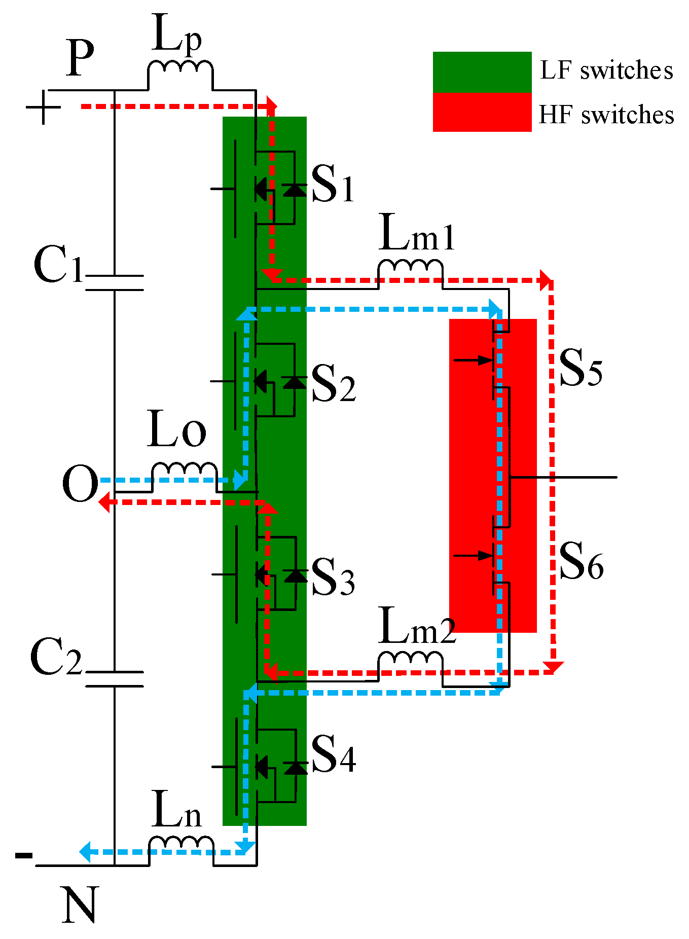
Figure 2.
Analysis of midpoint voltage deviation.
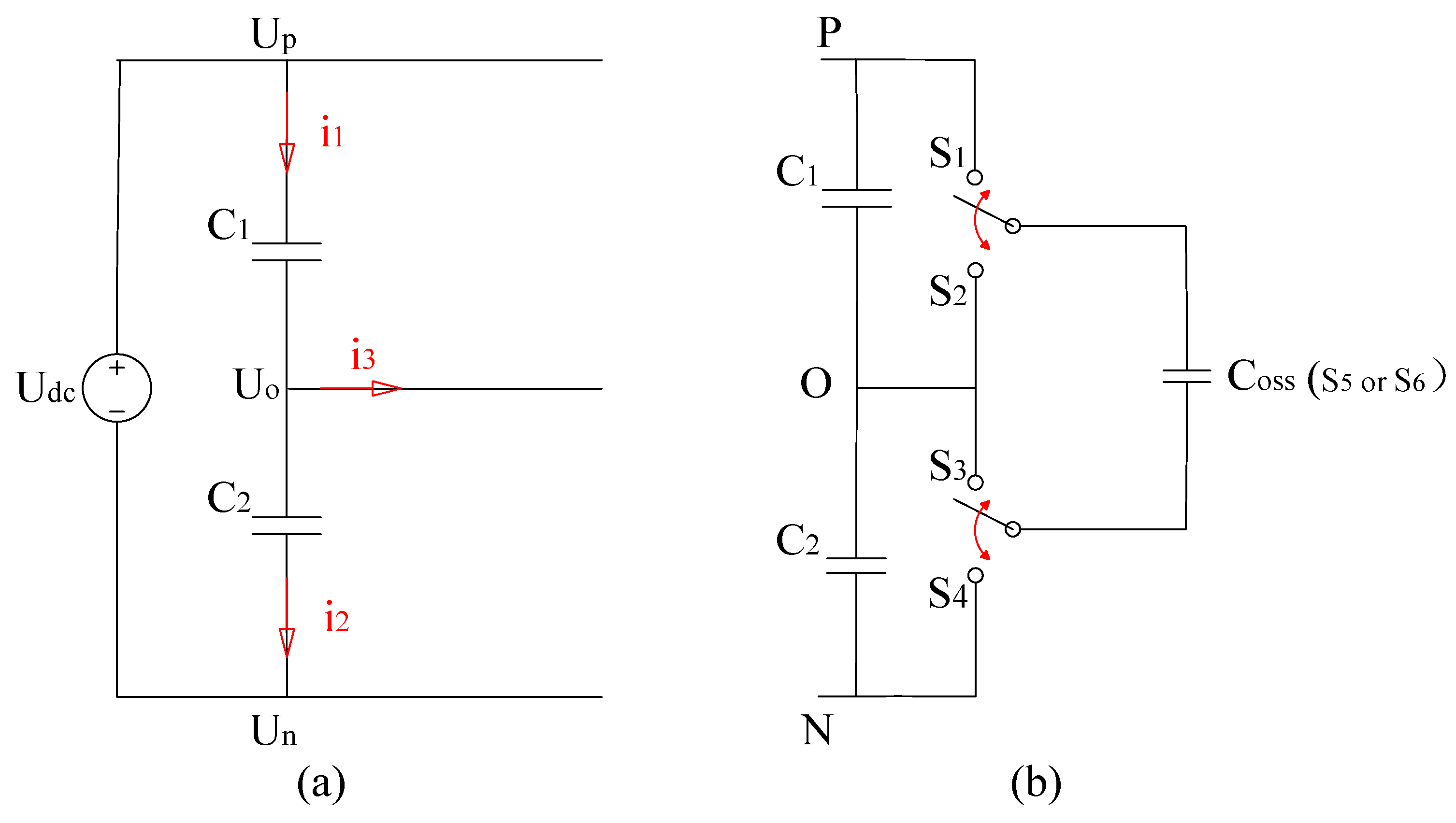
Figure 3.
Simulation Results of DC Bus Capacitor Voltage.
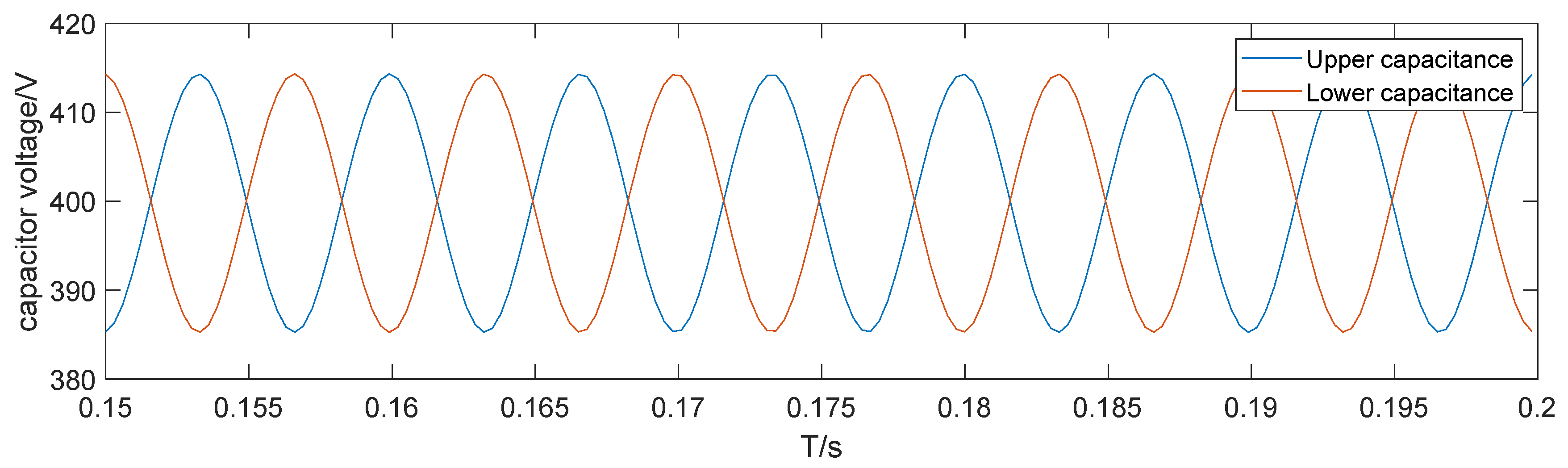
Figure 4.
The phenomenon of high-frequency switch input voltage jumping during LF switch switching.
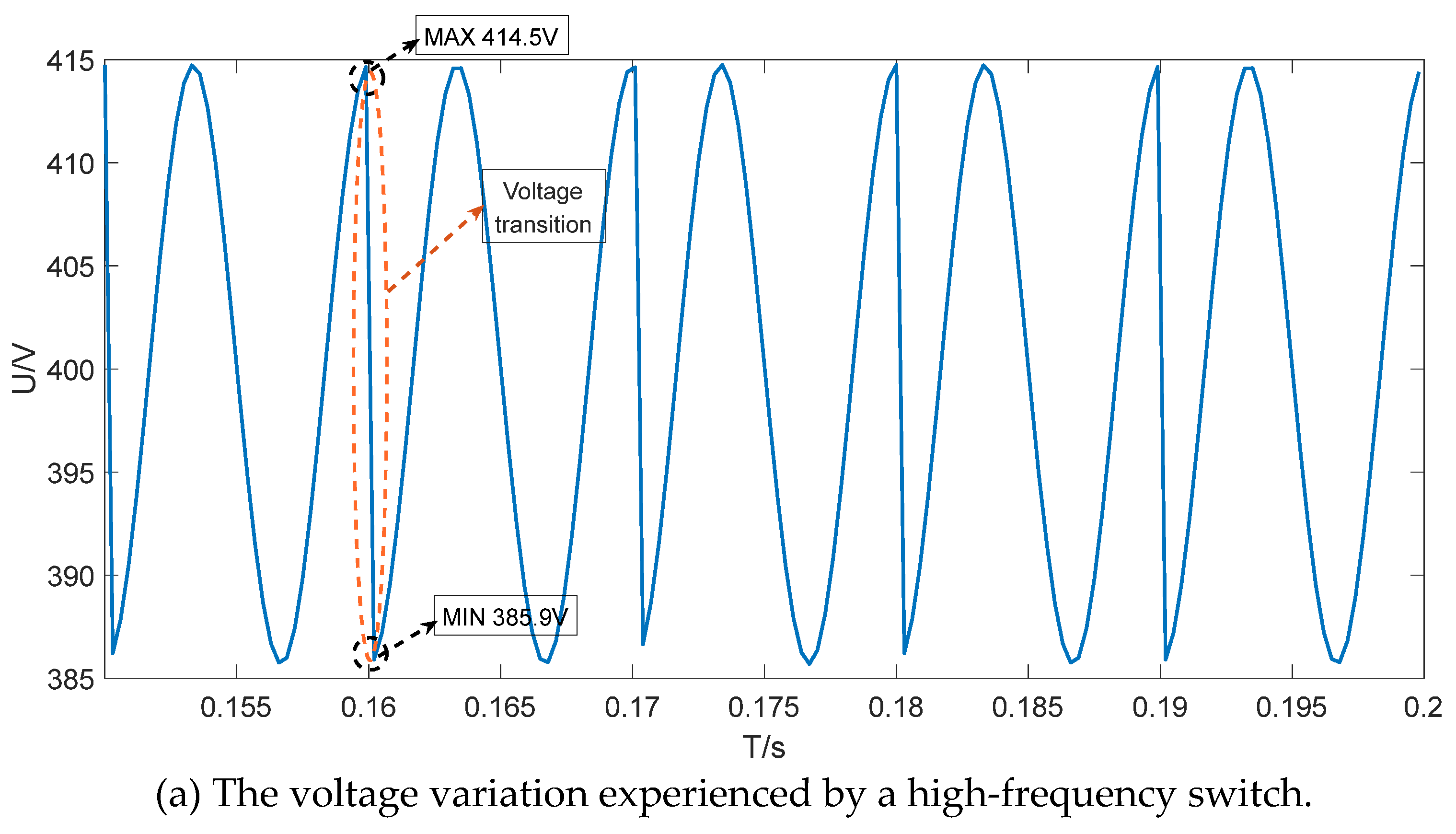
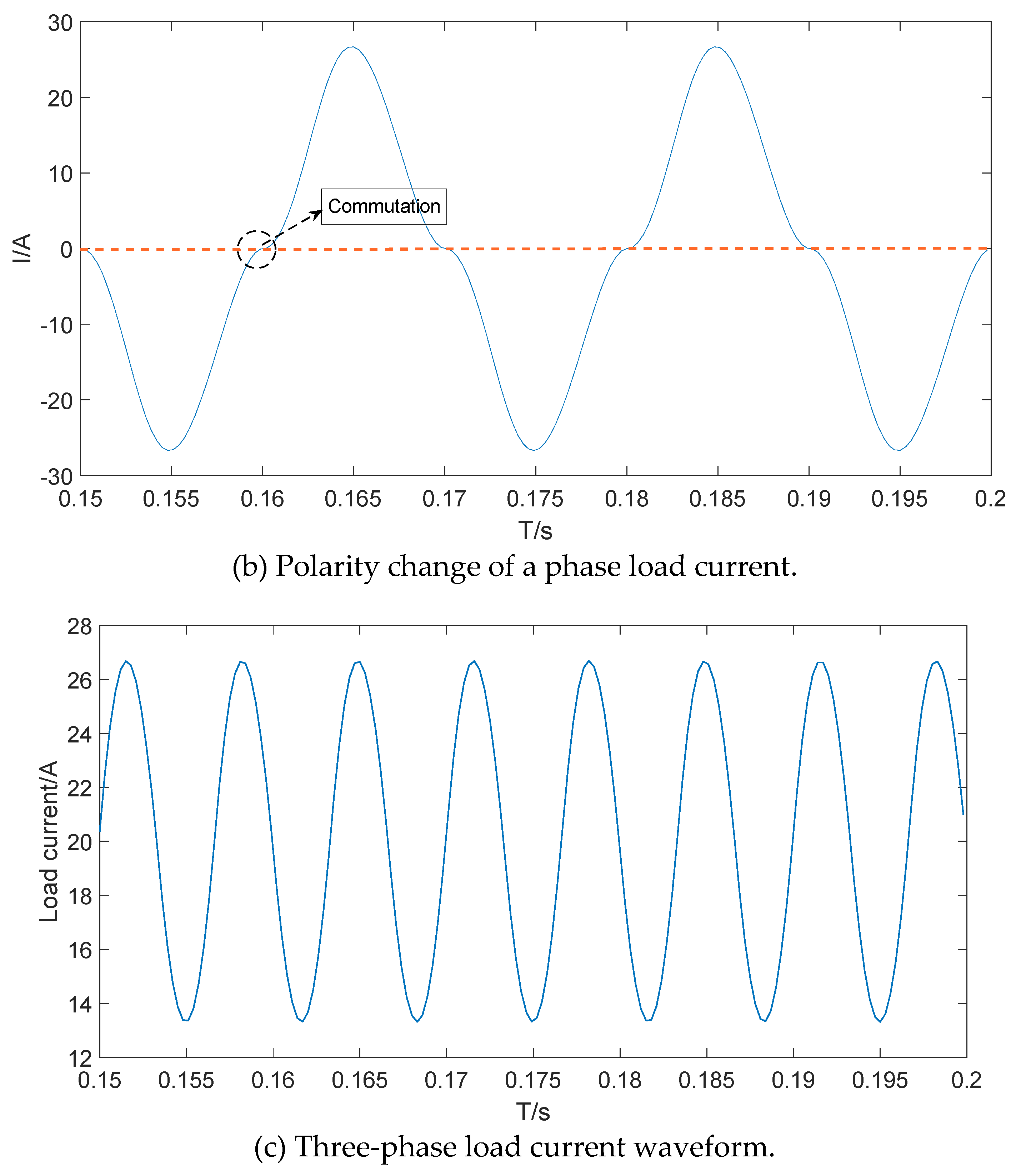
Figure 5.
Plot of voltage difference with DC capacitance.
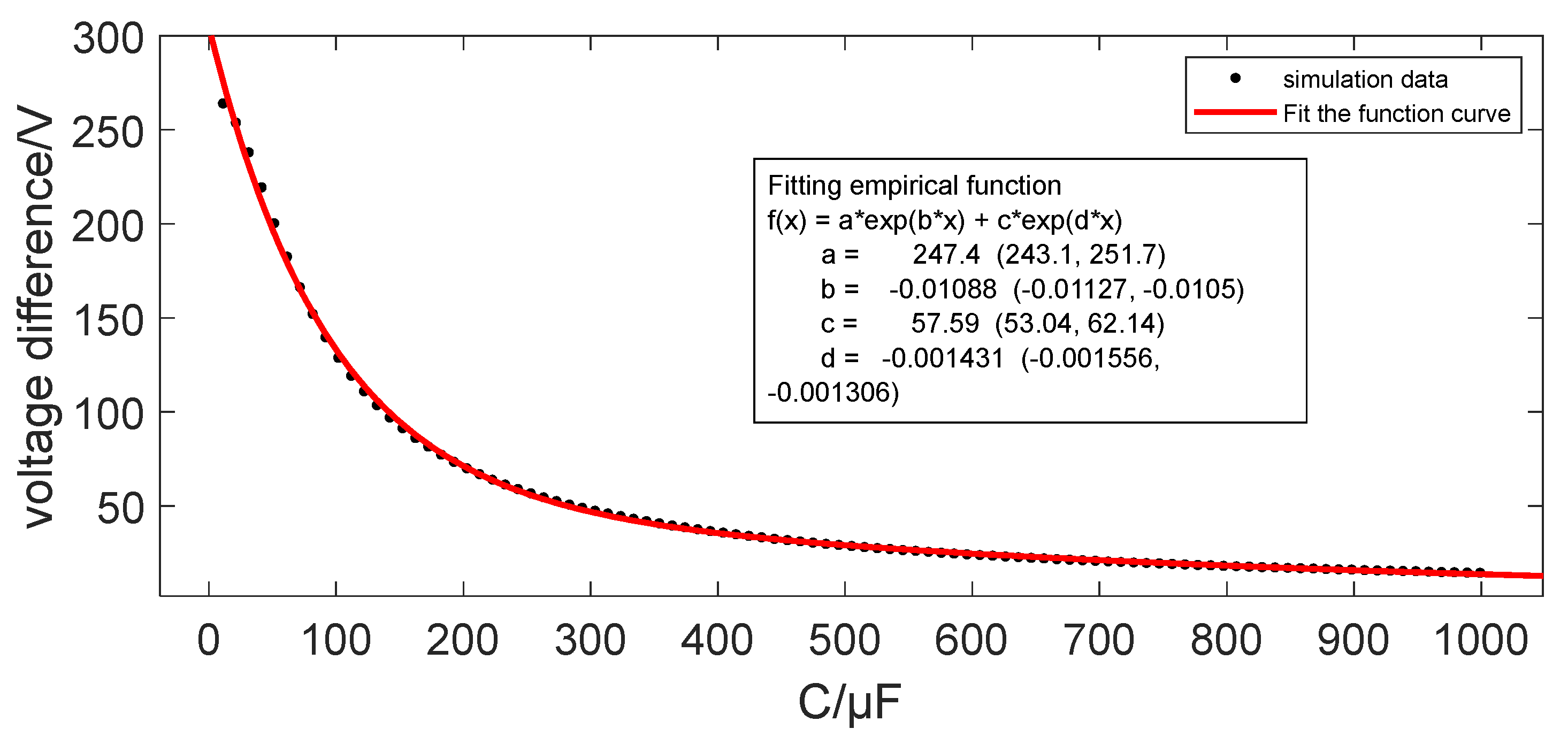
Figure 6.
Plot of voltage difference with power.
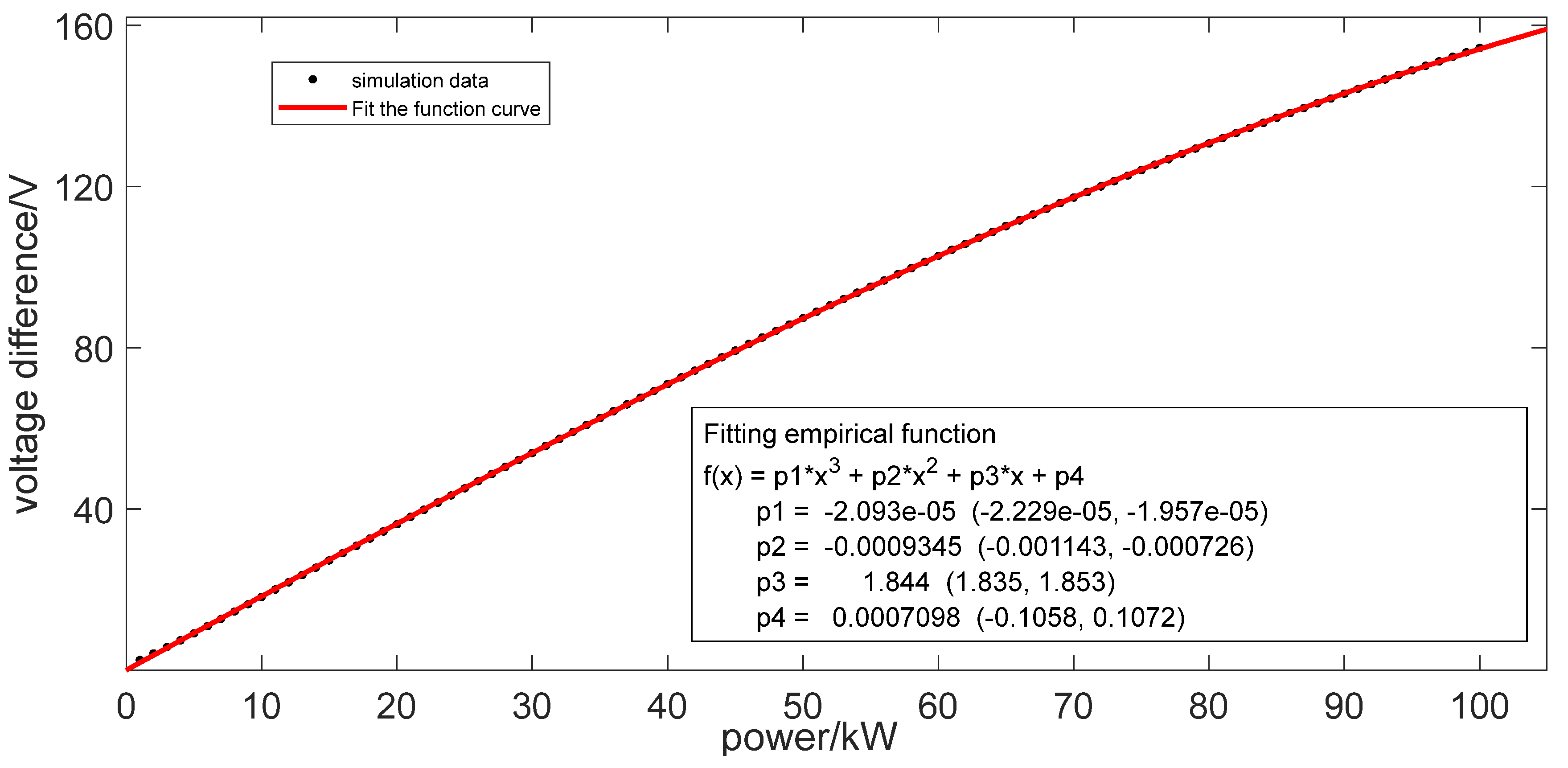
Figure 7.
The effect of different capacitances and powers on the voltage difference is measured during low-frequency switching.
Figure 7.
The effect of different capacitances and powers on the voltage difference is measured during low-frequency switching.
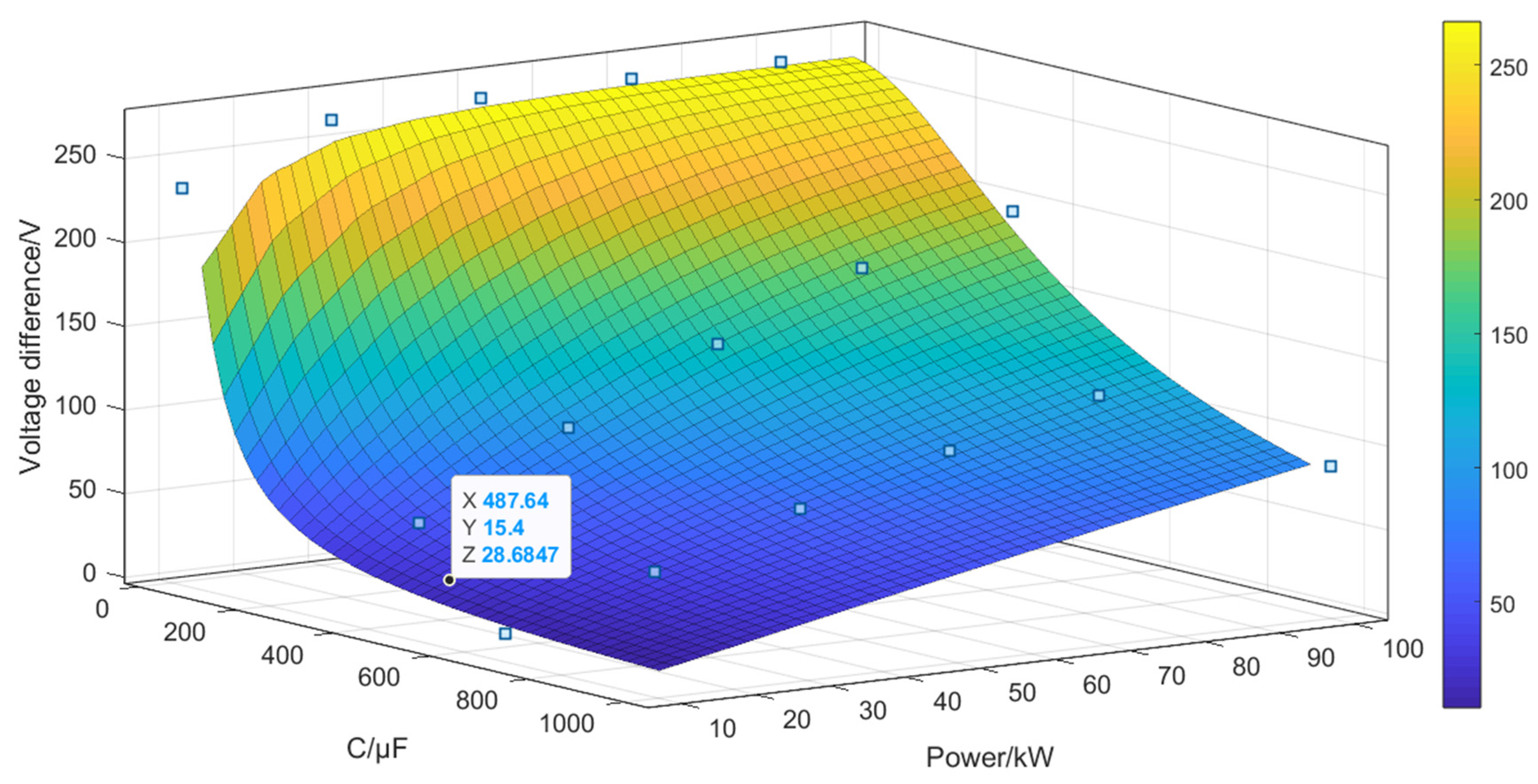
Figure 8.
The overvoltage absorption circuit proposed.
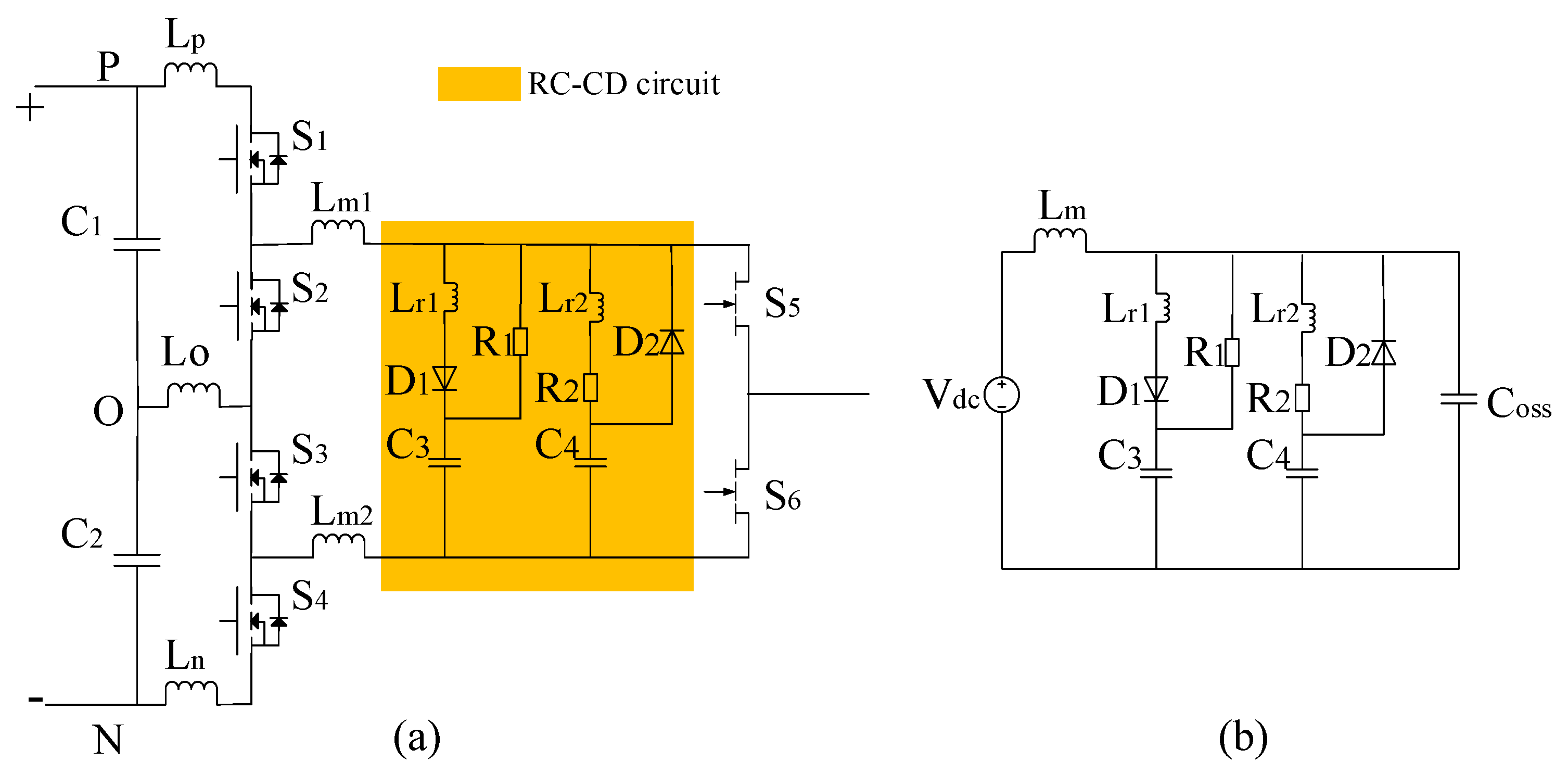
Figure 9.
The transient analysis process of the proposed circuit.
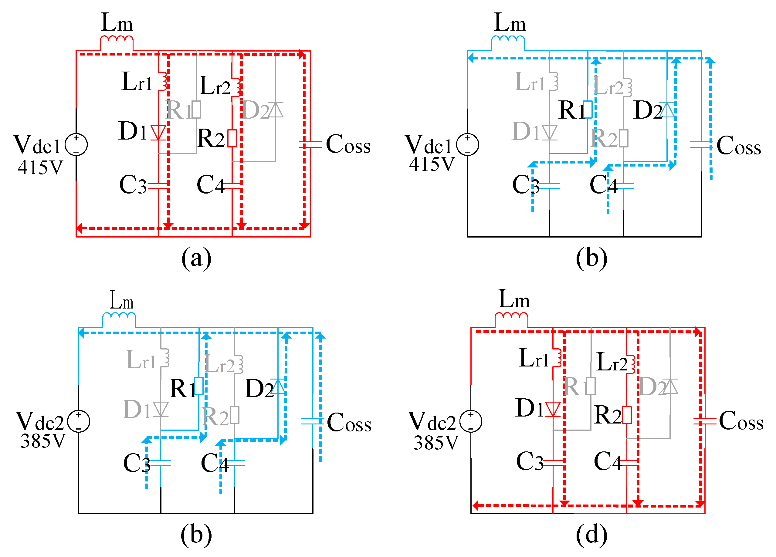
Figure 10.
Current waveforms of different inductors in the loop.
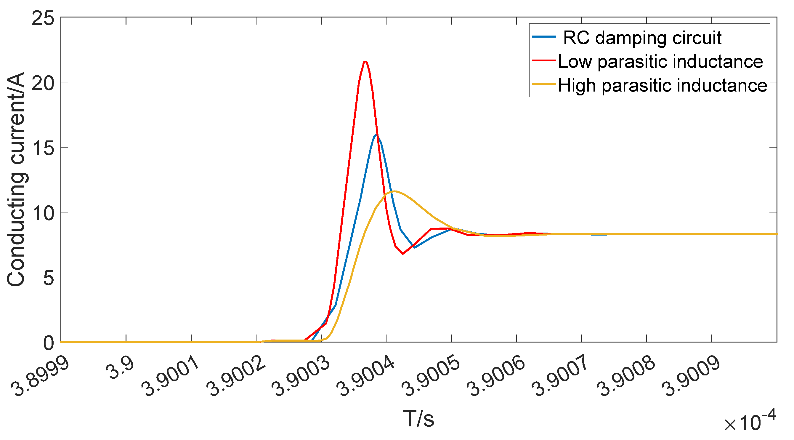
Figure 11.
Analysis of the three-level ANPC Electromagnetic Field Model.
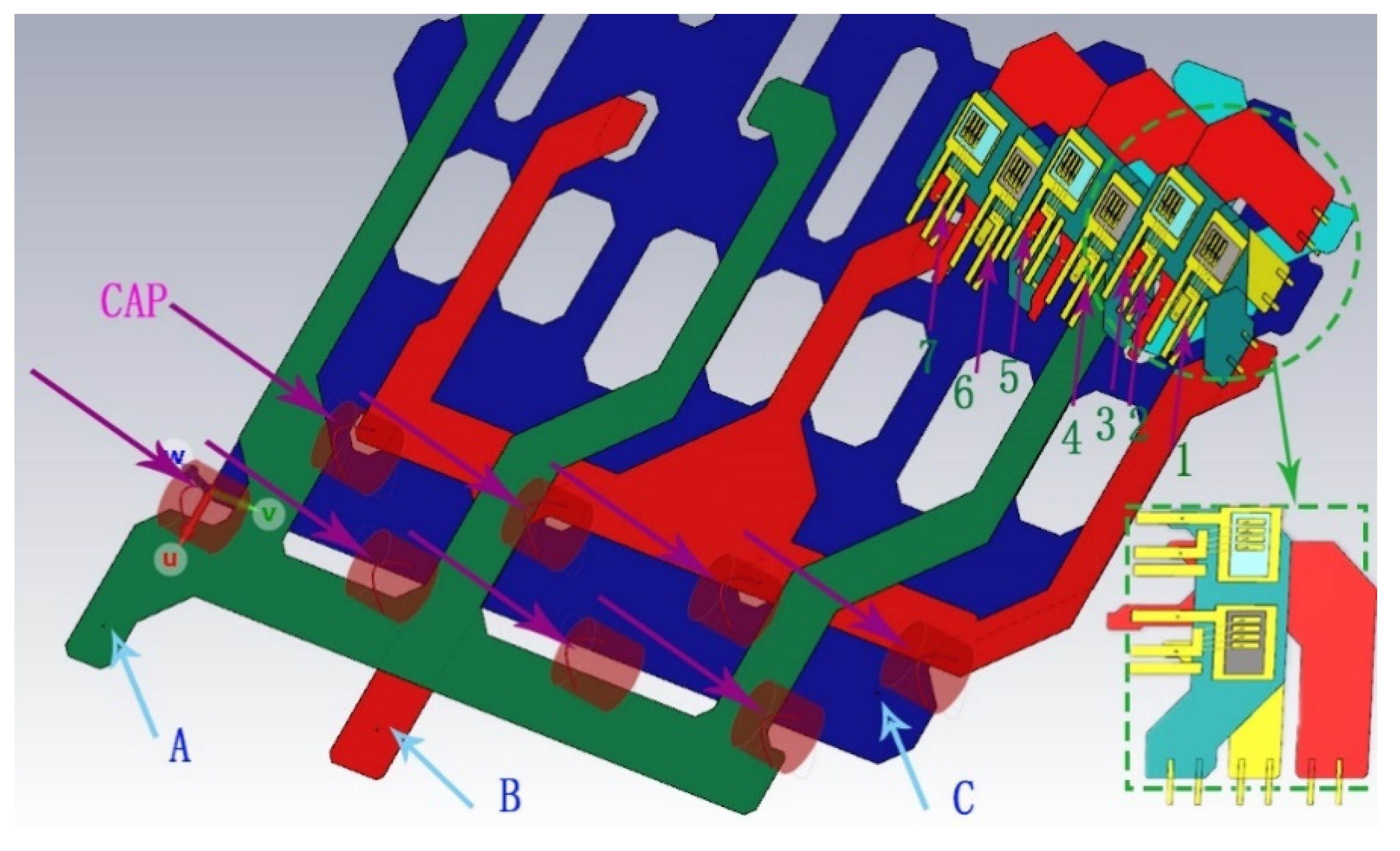
Figure 12.
Maximum switch voltage at different
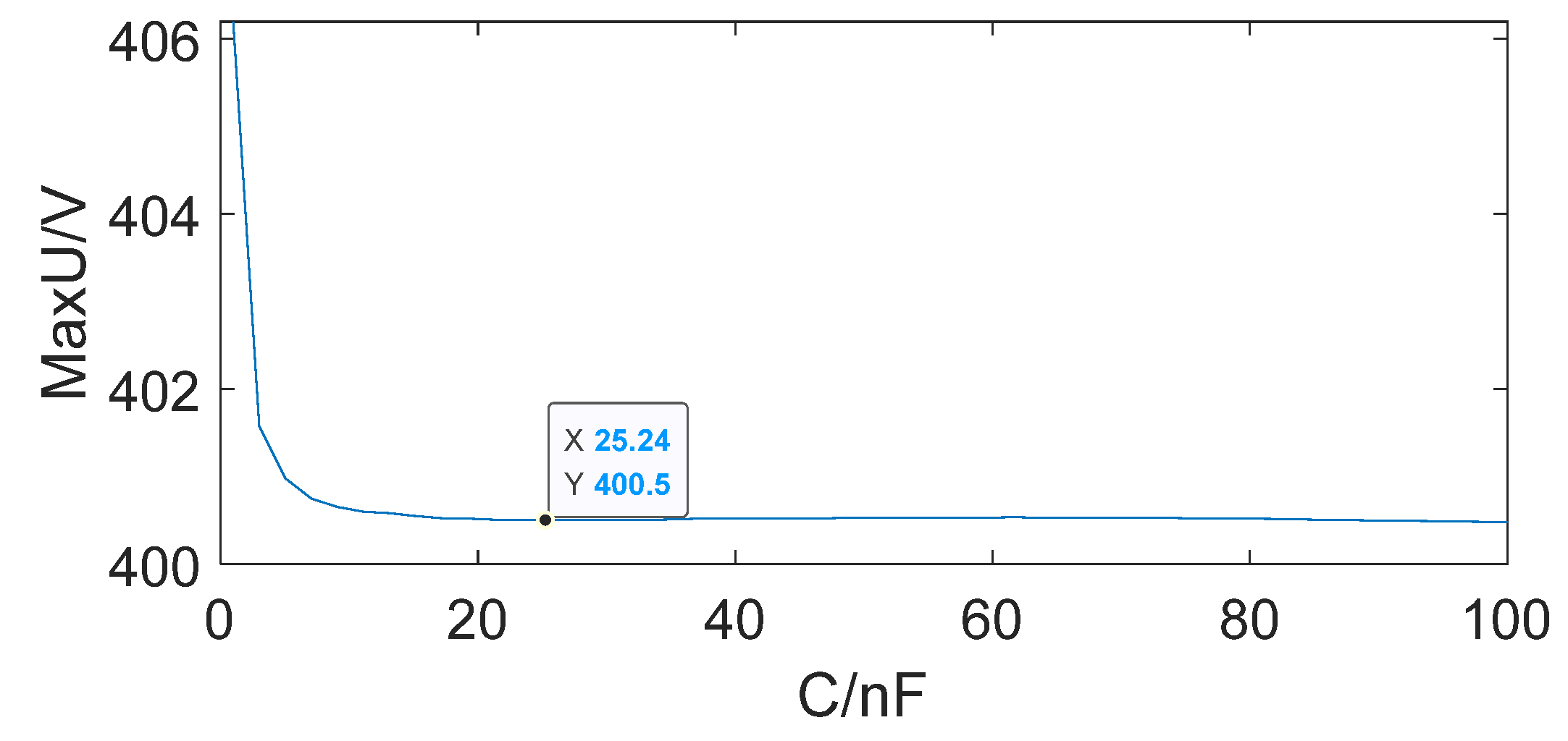
Figure 13.
three-level ANPC Switching Signal Modulation.
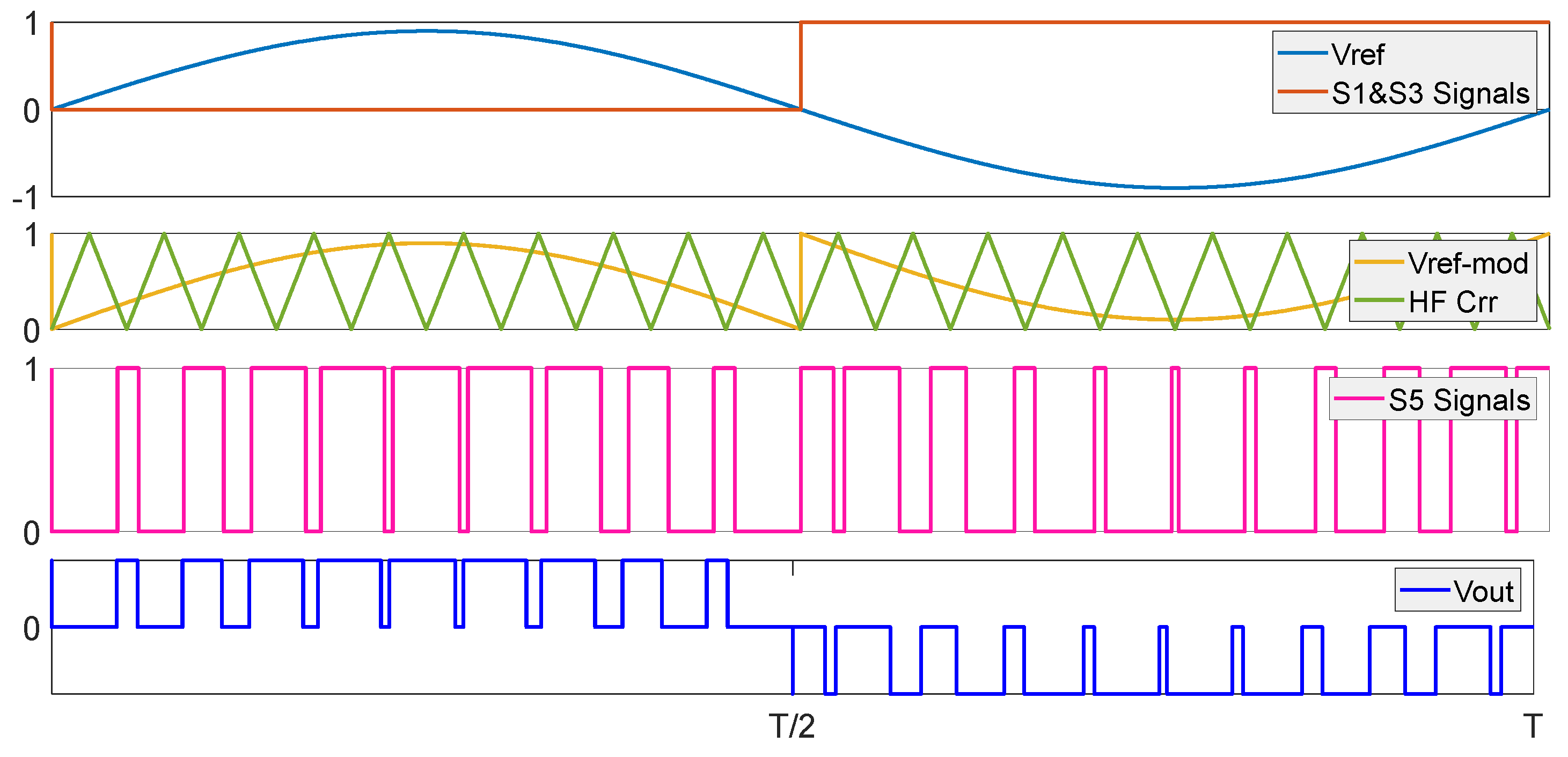
Figure 14.
Switching Mode of Parallel three-level ANPC.
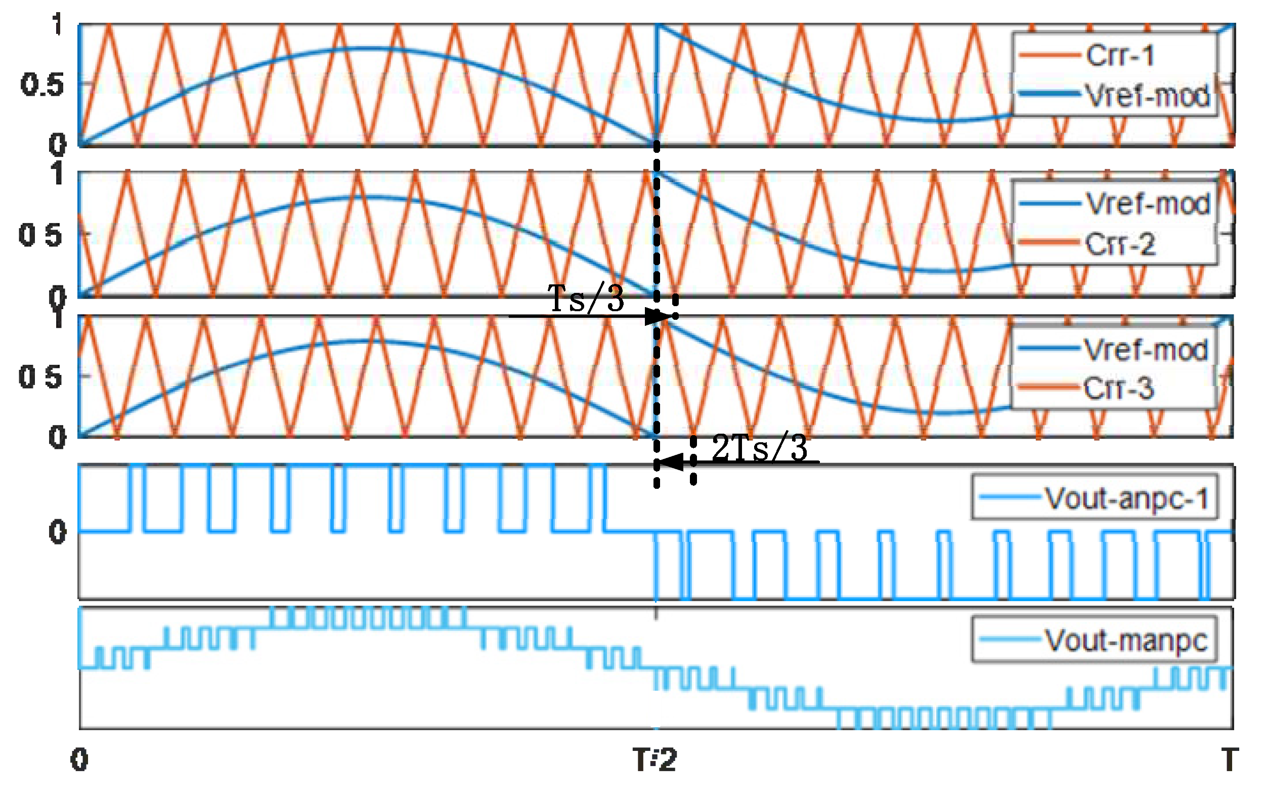
Figure 15.
(a) DC bus capacitor voltage waveform without any scheme. (b) DC bus capacitor voltage waveform with the scheme proposed in this paper.
Figure 15.
(a) DC bus capacitor voltage waveform without any scheme. (b) DC bus capacitor voltage waveform with the scheme proposed in this paper.
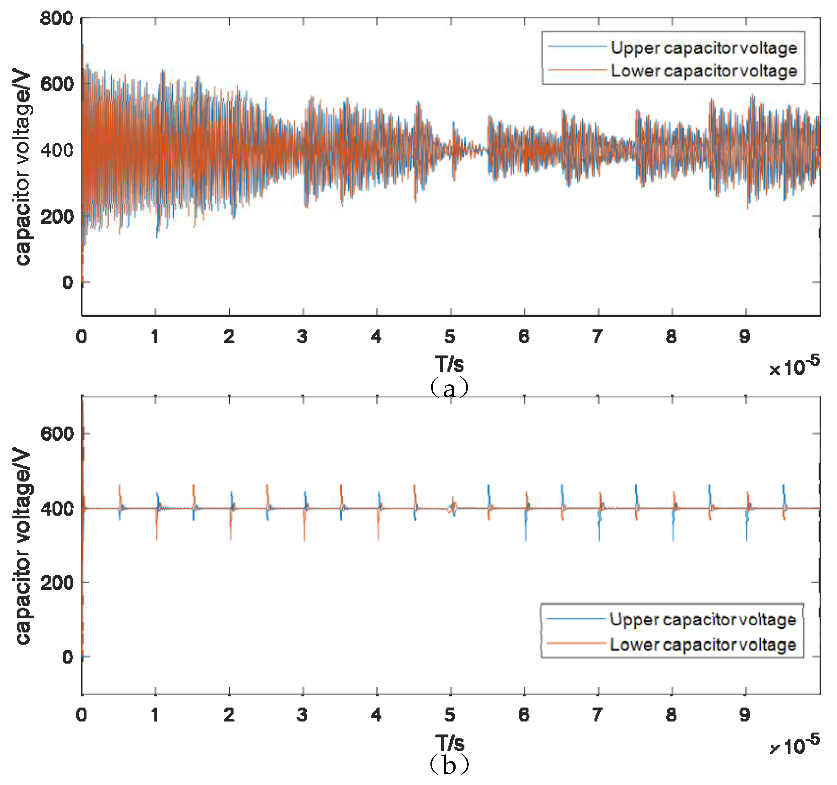
Figure 16.
Switching off voltage waveform under optimal component parameter conditions.
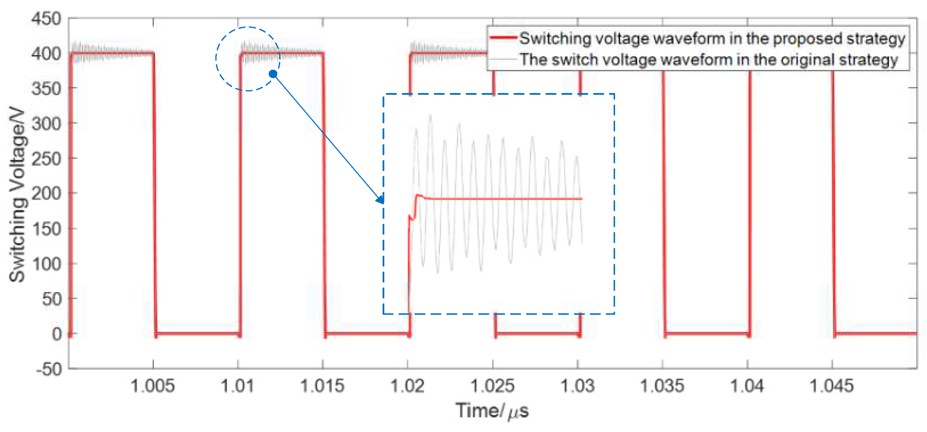

Table 1.
DIFFERENT HYBRID MODULATION TECHNIQUES FOR THREE-LEVEL ANPC.
| Hybrid Modulation technology | LF switches | HF switches |
|---|---|---|
| Group I | , , | |
| Group II | , , |
Disclaimer/Publisher’s Note: The statements, opinions and data contained in all publications are solely those of the individual author(s) and contributor(s) and not of MDPI and/or the editor(s). MDPI and/or the editor(s) disclaim responsibility for any injury to people or property resulting from any ideas, methods, instructions or products referred to in the content. |
© 2023 by the authors. Licensee MDPI, Basel, Switzerland. This article is an open access article distributed under the terms and conditions of the Creative Commons Attribution (CC BY) license (http://creativecommons.org/licenses/by/4.0/).
Copyright: This open access article is published under a Creative Commons CC BY 4.0 license, which permit the free download, distribution, and reuse, provided that the author and preprint are cited in any reuse.


