Preprint
Article

Undesired Operating Points and Hardware Trojans in High-Speed Operational Amplifier Microcircuits

Altmetrics

Downloads

71

Views

26

Comments

0

This version is not peer-reviewed

Submitted:

19 November 2023

Posted:

20 November 2023

You are already at the latest version

Alerts
Abstract
The classification of Trojans in modern analog microcircuits is considered. Using high-speed operational amplifiers (Op-Amps) as an example, the relationship between Op-Amp circuit design and the formation of undesirable states in typical switching circuits is shown. Circuit solutions are proposed to minimize the Trojan states of high-speed Op-Amps. These include limiting the maximum output currents of the input stages of the Op-Amp during the transient process and the use of differentiating transient correction circuits in the Op-Amp.
Keywords: 
Subject: Engineering  -   Electrical and Electronic Engineering

1. Introduction

Undesired Operating Points in a complex analog electronic circuit, known as “Trojans”, “hardware Trojans”, “hardware traps” or “Trojan states”, can cause the designed device circuitry to fail to perform to its stated specification [1,2]. Operational amplifiers (Op-Amps) are the main active element used in modern analog systems (ADC/DAC, active filters, etc.), and can also suffer from the Trojan state problem, incl. when using general feedback [1,2]. In particular, circuit engineering methods of increasing the slew rate (SR), associated with a dynamic increase in the output currents of the input stage, lead to Trojan states of high-speed Op-Amps [3,4,5,6,7]. In [8,9,10,11], several effective methods were proposed for detecting positive feedback loops (PFLs), as well as detecting all Trojan states in analog circuits. In [12], a new method for identifying PFLs in an analog circuit is shown. The essence of the method [12] is as follows: first, a list of circuit connections is created using graphs, and then the graphs are divided into strongly connected components. Graph theory methods are then used to detect all PFLs and identify unwanted operating points for associated components [12].
The process of detecting and eliminating Trojan states in an Op-Amps can be divided into three stages [1,2]: identifying positive feedback loops in the Op-Amp and identifying undesired operating points; search for all Trojans in the Op-Amp; modification of the Op-Amp circuit to remove Trojan states.
Publications [1,2] present a method for eliminating Op-Amp Trojan state caused by large-signal operation of the circuit by eliminating PFLs and undesired DC modes.
In [13], a high-speed Op-Amp modification was proposed with the inclusion of an additional capacitor, which temporarily increases the cascade currents, reducing the internal signal delay.
The results of the study [14,15] by scientists from Iowa State University presented several examples of dynamic analog hardware Trojans, both unintentional by design and intentionally built-in structures.
In [16,17,18] the main stages of development and supply of microcircuits are presented, in which Trojans can be introduced (intentionally or not) during circuit design, creation of topologies, copying and counterfeiting, and provides an overview of some existing topological solutions that have Trojan states.
In [19], a new circuit for determining the active current on a microcircuit chip was proposed, consisting of a current mirror, a current comparator with an adjustable threshold and a scanning register based on a multiplexer, which makes it possible to determine the beginning and termination of current switching in the power bus when temporary Trojans are triggered. When the Trojan state is activated during normal operation of the microcircuit, the measured characteristics of the power rails change dramatically, allowing anomalies to be detected. This on-site monitoring is especially useful for detecting complex Trojan conditions.
Changing the temperature of different areas of an analog microcircuit chip also makes it possible to detect some Trojan states [20].
Thus, at present, the development of microcircuits in which the so-called “Trojan states” are excluded [1,2,3,4,5,6,7,8,9,10,11,12,13,14,15,16,17,18,19,20,21,22,23,24,25,26], incl. in operational amplifiers with increased speed, in which these effects and undesirable operating points may arise not due to “deliberate hardware traps ” [23,24], but due to high currents during the period of forcing the recharging process of the correction capacitor, causing after some time the destruction of thin connecting connections conductors and overheating of transistors.

2. Energy limitations for input stages Op-Amp with maximum speed
For operational amplifiers with a classical architecture (Figure 1), the SR in large-signal mode is estimated using the equation [27,28]
SR = 2 π f unity V lim ,
where f unity is the unity gain frequency of the adjusted open-loop Op-Amp; V lim is limiting voltage of the transit characteristics of the input stage (IS).
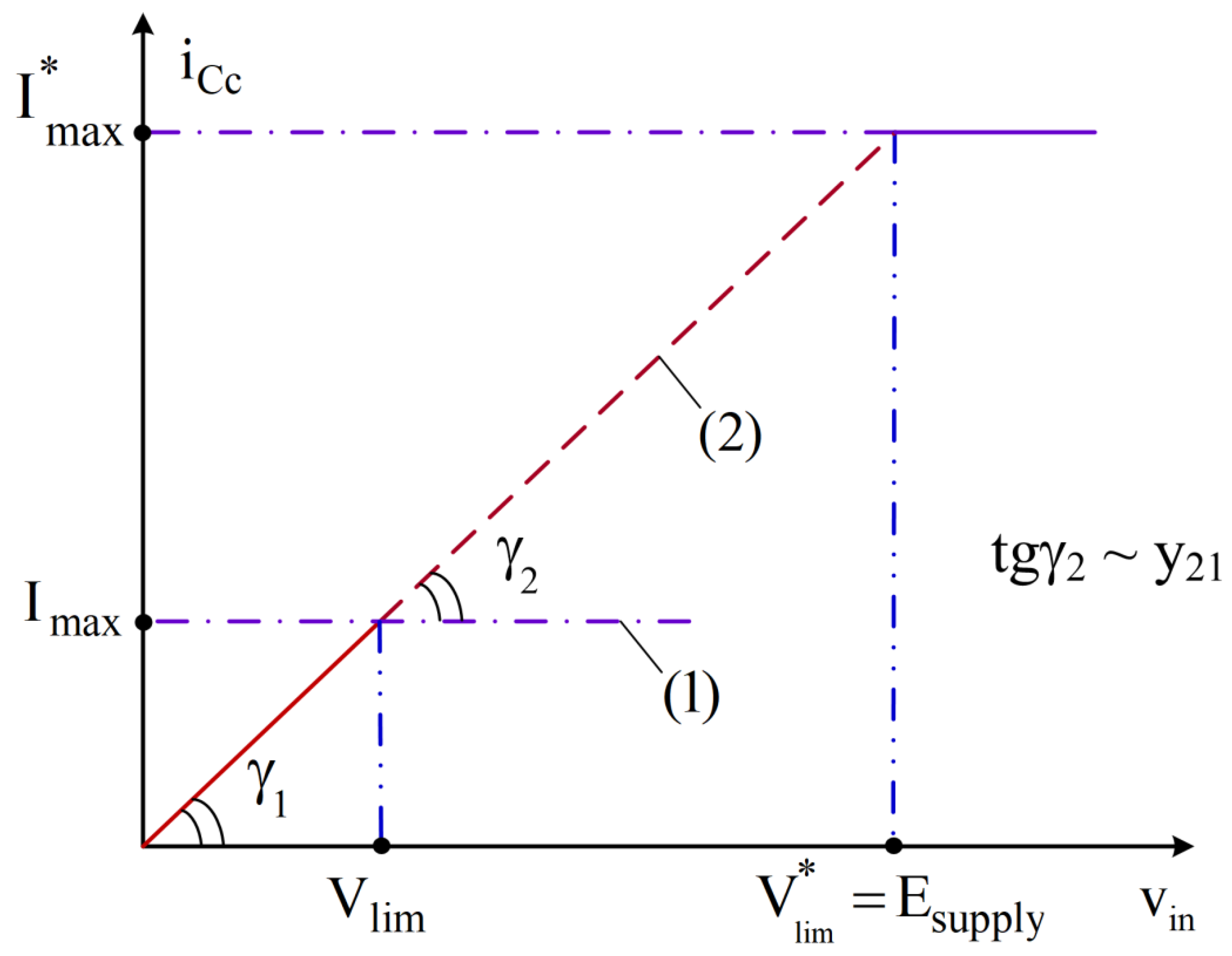
Typical values of Vlim of input stages on bipolar transistors are millivolts [29], and the small-signal slope of their transit characteristic y21 is quite significant
y 21 = I max V lim ,
where I max = I 0 is the maximum possible output current of the input stage, depending on the total current I0 of the common emitter circuit of the IS [29].
Figure 2. Transit characteristic of a classic differential operational amplifier (1) and differential operational amplifier with nonlinear correction (2).
Preprints 90886 g002
From (2) it follows that to increase SR it is necessary to increase Vlim, i.e., provide a linear mode of operation of the Op-Amp input stage over the entire range of changes in the input voltage vs, which can vary up to the value Vs=E(+)=E(-)=Esupply, where Esupply is the Op-Amp supply voltage. Typically, “extension” of the transit characteristic of the IS is ensured by nonlinear correction circuits [28,30].
The stability of the Op-Amp will not deteriorate if, when “extending” the transit characteristic, the angles of its inclination are preserved for small and large signals y1=y2, i.e., the equality will be satisfied:
I max V lim = I max * E supply .
Consequently, the maximum output current of the input stage, which has an extended active operating range to increase SR, can reach
I max * = E supply V lim I max .
So, if the input stage has I0=1mA, Esupply=15V, Vlim≈50mV, then the numerical values of the maximum output current are I max * 300 mA.
Thus, the transistors of the input stage of a high-speed op-amp must provide, at the time of the front of the transient process tf (usually t f 1 ÷ 10 ns), an output current commensurate with the typical values of the Op-Amp load current. It should be expected that this conclusion will require a revision of the prevailing ideas that the input stage of an Op-Amp is a micro-mode subcircuit. If you want to achieve extremely high performance, you will have to put up with the fact that the maximum output current of the IS should (for a short time) be measured in tens and sometimes hundreds of milliamps. This is the first problem that is not always taken into account when designing high-speed Op-Amps.
The second problem is related to the fact that any Op-Amp operating in the structure of complex analog-digital devices can (in atypical modes) for a fairly long time t p > > t f be overloaded at the input with large signals (for example, when turning on the power). In this case, for a sufficiently long time t p > > t f , voltages close to the supply voltage will be applied to the inputs of the Op-Amp, and therefore a large output current of the IS can cause thermal destruction of the current-carrying paths, overheating and failure of the IS transistors.
Thus, Op-Amps with extreme speed in the absence of special protection against excessively large output currents of the input stage cannot have high reliability.
If we proceed from energy limitations, i.e., assume that the input stage of the Op-Amp will not fail due to overheating during prolonged input overload, then the value of its maximum output current becomes known
I max * y 21 * E supply
and therefore, the slope of the transit characteristic
y 21 * y 21 . max I max * E supply P p E supply 2 ,
where Pp is the permissible power dissipated in the elements of the input stage during its overload time tp, and
P p E supply t p 0 t p i C c d t .
where iCc is the recharging current of the integrating capacitor Cc.
Thus, the slope of the gain of the input stage of a high-speed Op-Amp (the slope of its transit characteristic) cannot be selected without taking into account the thermal effects in the microcircuit. However, this parameter (y21) of the input stage has a significant impact on many dynamic parameters of the Op-Amp [27,28,29], including:
y 21 . max y 21 = I 0 V lim ,   ω 1 = y 21 C c ,   LG = GA I N = y 21 R c ,
where y 21 is the small-signal slope of the base input stage before the introduction of a nonlinear correction circuit; ω 1 = 2 π f 1 is small-signal frequency of unity gain of the Op-Amp; R c is equivalent resistance connected in parallel with Cc; LG is loop gain of the Op-Amp, numerically equal to the gain of the input stage.
Therefore, under the considered restrictions, the unity gain frequency of a reliable high-speed Op-Amp cannot exceed the value
ω 1 ω max = P p C c E supply 2 .
The (9) shows that with Pp=const, y21= const the main natural way to increase ω1 and SR is to reduce the capacitance of the correction capacitor Cc. However, this is a rather complex problem associated with a decrease in the absolute values of high-frequency time constants and their number at the input and output stages of the Op-Amp, feedback elements, and load. Ultimately, Cc is determined mainly by technological advances – high-frequency parameters of integrated transistors, capacitances on the substrate, collector-base capacitances of transistors, etc.
Physical restrictions on the Op-Amp slew rate with a quasi-linear input stage and input signals with an amplitude close to the supply voltage are the capacitances on the substrate of the IS transistors and the permissible power dissipated on the elements of the input stage during its long-term overload (Pp). Note that this conclusion was made in the absence of current protection at the input stage and the range of its active operation is close to Esupply ( V lim * E supply ).
It should be noted that traditional Op-Amp protection circuits at the input [31] protect its input transistors from breakdown of the emitter-base p-n junction, but limit the range of changes in input signals at the level of Vlim≈0.6÷0.7 V. This does not allow obtaining extremely high performance, commensurate with speed of the Op-Amp for linear mode, since in this case SR * = 2 π f 1 V lim 1.4 π f 1 [V/s].
Thus, developers of high-speed Op-Amps have to seek a compromise between the reliability of the Op-Amp in any mode (feedback interruption, short-term shutdown of one of the power sources, operation of the Op-Amp in signal comparator mode, etc.) and maximum performance. It is problematic to implement these two qualities within the framework of traditional circuit solutions.

3. Intelligent protection against Trojans in Op-Amps with current feedback

Figure 3 shows the architecture of a high-speed Op-Amp with current negative feedback, the peculiarity of which is the creation of “smart” protection of the input stage, which does not affect the operation of the circuit during the front of the transient process tf, but limits the output currents of the input stage in the event that the voltage at the input of the Op-Amp it operates for a longer time.
The op-amp circuit with current feedback (Figure 3) includes an input stage (Q1÷Q3) with large output current values
I max * β 3 I 1 2 ,
where β 3 is the base current gain of the double-collector transistor Q3; I1 is static value of the output current of the reference current source I1, controlled by the “Off” input.
Condition (14) is satisfied if the input signal is large enough: V s . max β 3 I 1 R 1 R 2 .
The circuit in Figure 3 provides nonlinear negative feedback, which shuts down the reference current source (RCS) if the current in the measuring resistor R0 exceeds the specified value Ilim. At the same time, I1 decreases, which limits the output current of the input stage at a given level I lim < I max * . As a consequence, the maximum rate of rise of the output voltage of an Op-Amp with such a IS is less than the maximum possible and is determined by the equation
SR * = 2 π f unity I lim R 1 R 2 .
Adjustment of the inertia of the IS output current limiting loop is provided by capacitor C0. It must be selected in such a way that the current protection does not operate during the edge of the input pulse signal, and its activation occurs at t p > > t f , i.e., when essentially nonlinear operating modes arise in the Op-Amp circuit and overheating of the crystal is possible.

4. Method for limiting the maximum output current in quad-core differential stages

Control of the maximum output current of the input stage of a high-speed Op-Amp implemented on a quad-core IS [32] (Figure 4) can be carried out either by appropriately selecting the factors of the product I1β3, or by introducing special current-limiting resistors R 1 = R 3 .
In this circuit, the input stage limiting voltage depends on the product
V lim * R 1 I 1 = R 3 I 2 .
At the same time, the slope of the IS transit characteristic on small and large signals is determined by resistor R2:
y 21 R 2 1 .
Therefore, the slew rate of an Op-Amp with such a IS
SR * = 2 π f unity R 1 I 1 .
In work [30] it is shown that in order to reduce the maximum possible output currents of a differential cascade in high-speed Op-Amps, it is possible to include special input voltage limiters, which are implemented by back-to-back parallel connection of several p-n junctions, as well as inductive diode elements.

5. Current protection in bridge input stages of high-speed Op-Amps

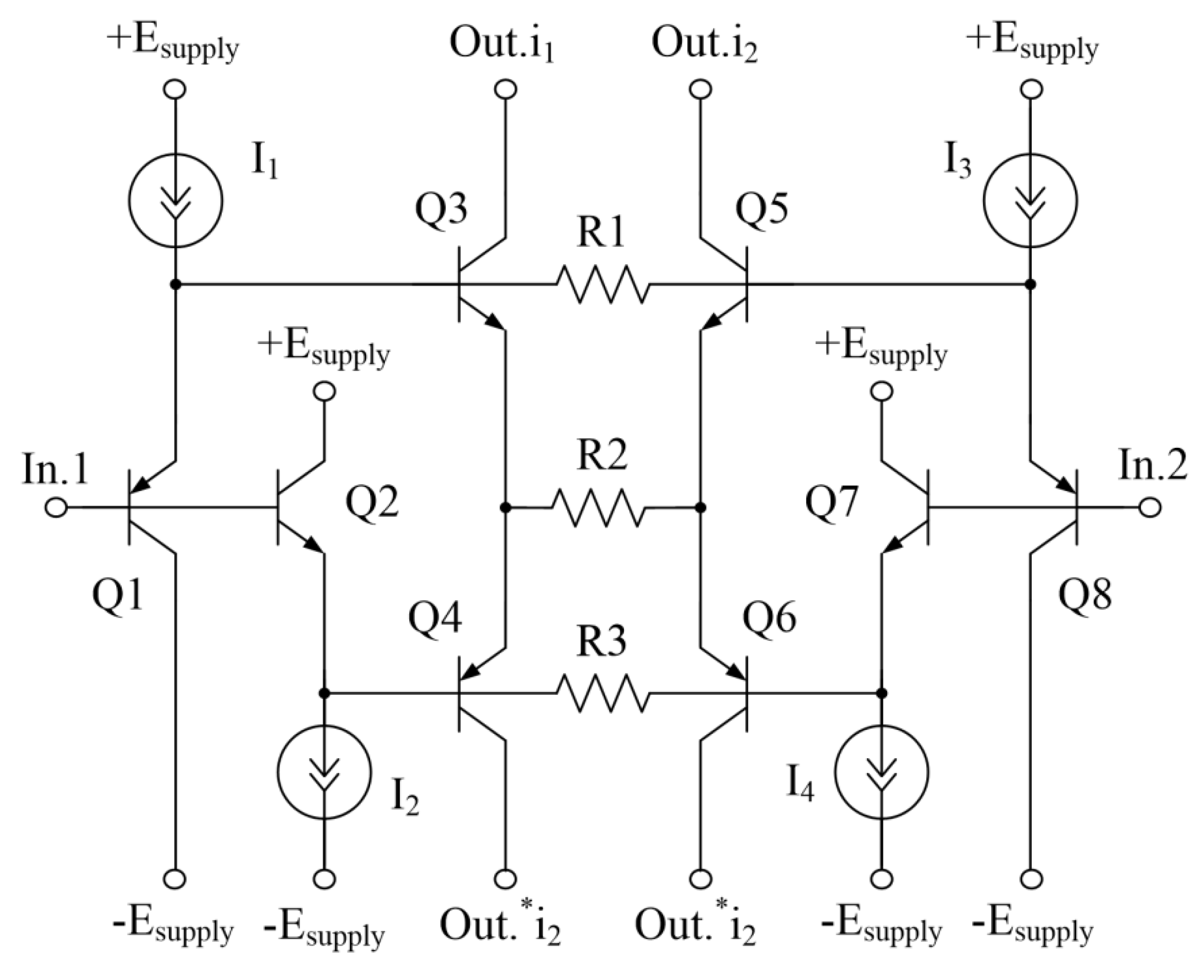
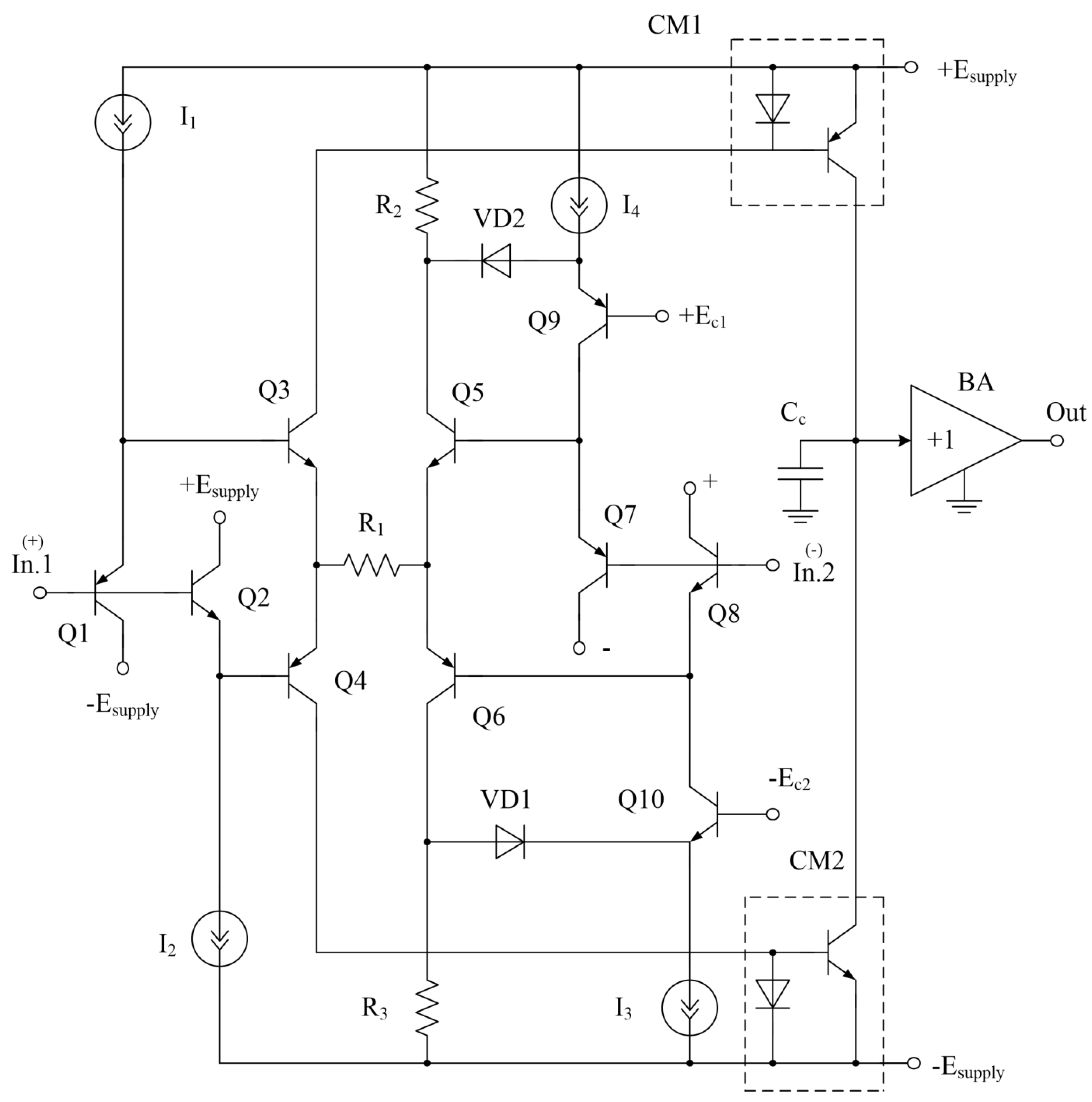
In the Op-Amp circuit in Figure 5, implemented on the basis of a bridge input stage, the IS current protection is performed on elements R2, VD2 (R3, VD1).
As soon as the collector current of transistor Q5 (Iс5) reaches the specified value
I lim E c 1 R 2 ,
transistor Q9 begins to turn off, which prevents a further increase in Ic5. Therefore, in such an Op-Amp the slew rate is
SR * = 2 π f unity R 1 R 2 E c 1
Thus, when designing an Op-Amp with the highest possible speed, it is necessary to pay attention to the energy of not only the output stages, but also the input stages, and also use special protection circuits that limit the maximum output current of the IS during the front of the transient process.

6. Trojan states in Op-Amps with differentiating transient correction circuits in large-signal mode

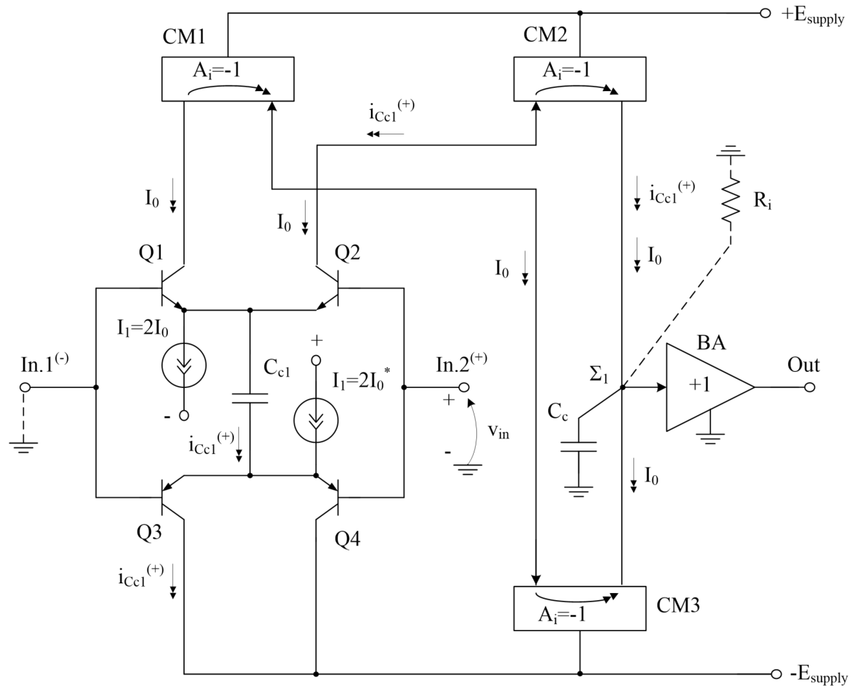
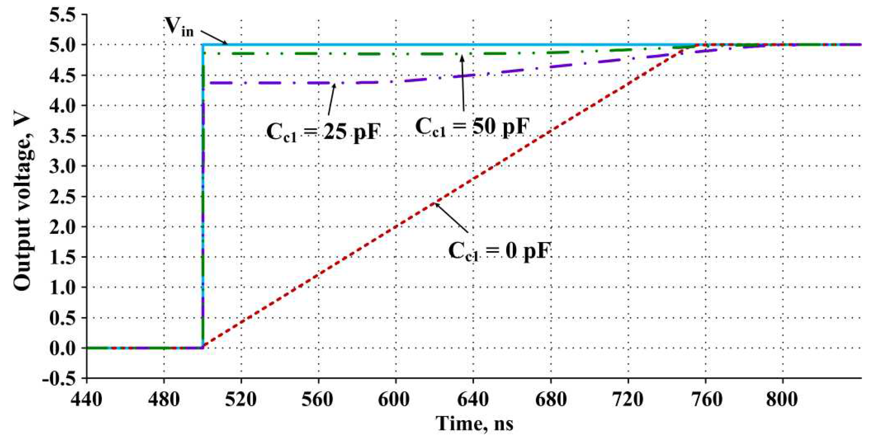
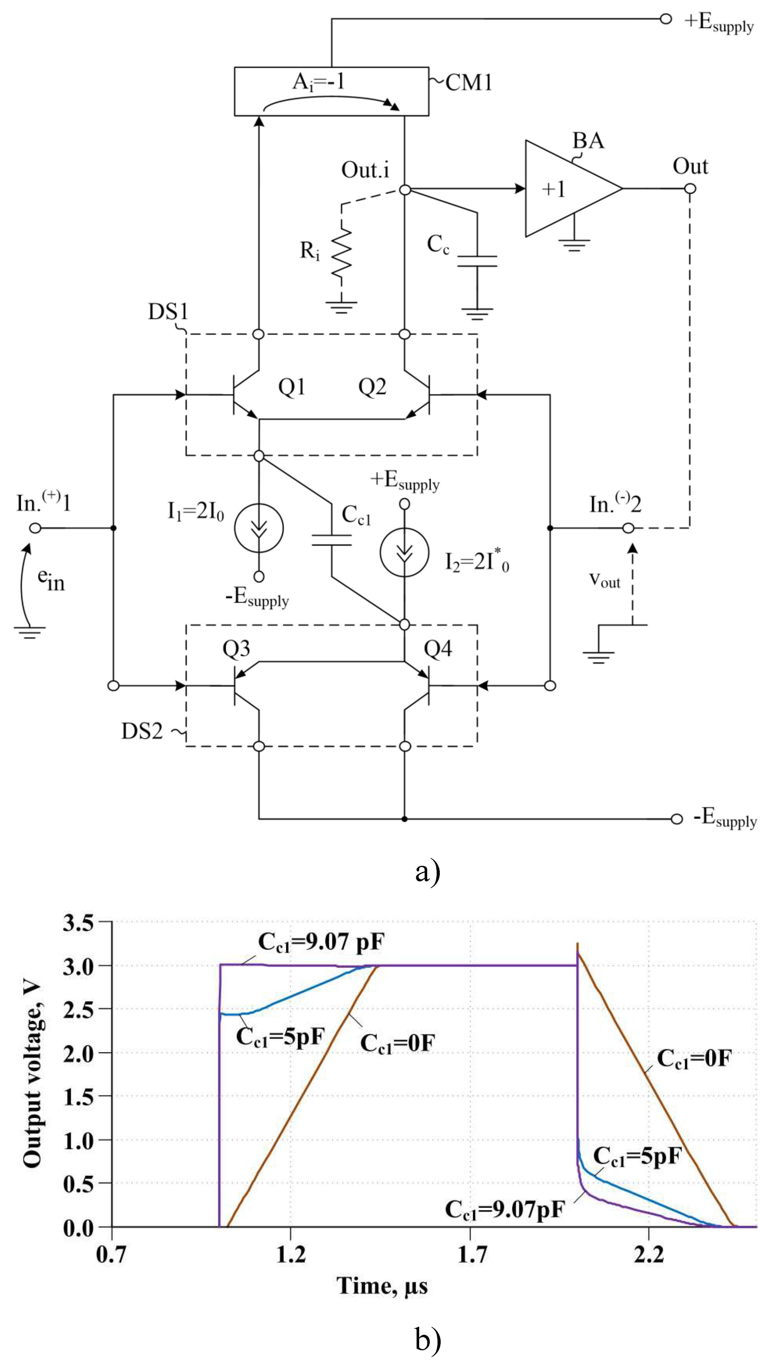
One of the promising methods for increasing the performance of Op-Amps is the use of differentiating circuits for correction of the transient process [33,34,35,36,37]. An example of the construction of such an Op-Amp and the results of its computer simulation are presented in Figure 6 and Figure 7.
Op-amp in Figure 6 contains the main differential stage Q1, Q2, three current mirrors CM1÷CM3 and a buffer amplifier BA. An additional differential cascade Q3, Q4 and a differentiating capacitor Cc1 ensures forced recharging of the capacitance of the integrating capacitor Cc, which increases SR (Figure 7).
An essential feature of the circuit in Figure 6 is that it eliminates Trojan states associated with high levels of DC output currents, which reduces overheating of transistors.
The considered Op-Amp circuit with a differentiating correction circuit has several modifications (Figure 8).
Thus, a promising circuit solution for high-speed Op-Amps, in which Trojan states are excluded due to excessively high DC currents, is the use of differentiating transient correction circuits.

7. Conclusions

A review of literature sources and a classification of Trojans in modern analog microcircuits are provided. Using high-speed operational amplifiers as an example, the relationship between Op-Amp circuit design and the formation of undesirable states in typical switching circuits is shown. Circuit solutions have been proposed that allow minimizing the Trojan states of high-speed Op-Amps, incl. limitation of the maximum output currents of input stages with nonlinear correction and the use of differentiating transient correction circuits in the Op-Amp.
The research has been carried out at the expense of the Grant of the Russian Science Foundation (project No. 22-29-00637).

References

  1. C. Cai and D. Chen, “Performance enhancement induced Trojan states in op-amps, their detection and removal,” 2015 IEEE International Symposium on Circuits and Systems (ISCAS), Lisbon, Portugal, 2015, pp. 3020–3023. [CrossRef]
  2. C. Cai and D. Chen, “A slew-rate enhancement technique for fully differential amplifier without inducing Trojan state,” 2015 IEEE 58th International Midwest Symposium on Circuits and Systems (MWSCAS), Fort Collins, CO, USA, 2015, pp. 1–4. [CrossRef]
  3. A. J. Lopez-Martin, S. Baswa, Jaime Ramirez-Angulo and R. G. Carvajal, “Low-Voltage Super class AB CMOS OTA cells with very high slew rate and power efficiency,” in IEEE Journal of Solid-State Circuits, vol. 40, no. 5, pp. 1068–1077, May 2005. [CrossRef]
  4. Huang and, D. B. Chen, “A simple slew rate enhancement technique with improved linearity and preserved small signal performance,” 2014 IEEE 57th International Midwest Symposium on Circuits and Systems (MWSCAS), College Station, TX, USA, 2014, pp. 270–273. [CrossRef]
  5. M. G. Degrauwe, J. Rijmenants, E. A. Vittoz and H. J. De Man, “Adaptive biasing CMOS amplifiers,” in IEEE Journal of Solid-State Circuits, vol. 17, no. 3, pp. 522–528, June 1982. [CrossRef]
  6. B. W. Lee and B. J. Sheu, “A high slew-rate CMOS amplifier for analog signal processing,” in IEEE Journal of Solid-State Circuits, vol. 25, no. 3, pp. 885–889, June 1990. [CrossRef]
  7. R. Harjani, R. Heineke and Feng Wang, “An integrated low-voltage class AB CMOS OTA,” in IEEE Journal of Solid-State Circuits, vol. 34, no. 2, pp. 134–142, Feb. 1999. [CrossRef]
  8. Y. -T. Wang, D. Chen and R. L. Geiger, “Practical methods for verifying removal of Trojan stable operating points,” 2013 IEEE International Symposium on Circuits and Systems (ISCAS), Beijing, China, 2013, pp. 2658–2661. [CrossRef]
  9. Z. Liu, Y. Li, R. L. Geiger and D. Chen, “Auto-identification of positive feedback loops in multi-state vulnerable circuits,” 2014 IEEE 32nd VLSI Test Symposium (VTS), Napa, CA, USA, 2014, pp. 1–5. [CrossRef]
  10. Z. Liu, Y. Li, Y. Duan, R. L. Geiger and D. Chen, “Identification and break of positive feedback loops in Trojan States Vulnerable Circuits,” 2014 IEEE International Symposium on Circuits and Systems (ISCAS), Melbourne, VIC, Australia, 2014, pp. 289–292. [CrossRef]
  11. Y. Li and D. Chen, “Efficient analog verification against Trojan states using divide and contraction method,” 2014 IEEE International Symposium on Circuits and Systems (ISCAS), Melbourne, VIC, Australia, 2014, pp. 281–284. [CrossRef]
  12. Z. Liu, Y. Li, Y. Duan, R. L. Geiger and D. Chen, “Identification and break of positive feedback loops in Trojan States Vulnerable Circuits,” 2014 IEEE International Symposium on Circuits and Systems (ISCAS), Melbourne, VIC, Australia, 2014, pp. 289–292. [CrossRef]
  13. A. Catania, M. Cicalini, M. Dei, M. Piotto, P. Bruschi, “Performance Analysis and Design Optimization of Parallel-Type Slew-Rate Enhancers for Switched-Capacitor Applications,” in Electronics, 2020, vol. 9, no. 11, pp. 1949. [CrossRef]
  14. Q. Wang, R. L. Geiger and D. Chen, “Hardware Trojans embedded in the dynamic operation of analog and mixed-signal circuits,” 2015 National Aerospace and Electronics Conference (NAECON), Dayton, OH, USA, 2015, pp. 155–158. [CrossRef]
  15. Y. Jin, D. Maliuk, Y. Makris, “Hardware Trojan detection in analog/RF integrated circuits,” in Secure System Design and Trustable Computing, 2016, pp. 241–268. [CrossRef]
  16. Y. Li and D. Chen, “Efficient analog verification against Trojan states using divide and contraction method,” 2014 IEEE International Symposium on Circuits and Systems (ISCAS), Melbourne, VIC, Australia, 2014, pp. 281–284. [CrossRef]
  17. A. Antonopoulos, C. Kapatsori and Y. Makris, “Trusted Analog/Mixed- Signal/RF ICs: A Survey and a Perspective,” in IEEE Design & Test, vol. 34, no. 6, pp. 63–76, Dec. 2017. [CrossRef]
  18. M. M. Alam, S. Chowdhury, B. Park, D. Munzer, N. Maghari, M. Tehranipoor, D. Forte, “Challenges and opportunities in analog and mixed signal (AMS) integrated circuit (IC) security,” in Journal of Hardware and Systems Security, 2018, vol. 2, pp. 15–32. [CrossRef]
  19. Y. Cao, C. -H. Chang and S. Chen, “A Cluster-Based Distributed Active Current Sensing Circuit for Hardware Trojan Detection,” in IEEE Transactions on Information Forensics and Security, vol. 9, no. 12, pp. 2220–2231, Dec. 2014. [CrossRef]
  20. M. Onabajo, Y.-B. Kim, “Method to use on-chip temperature sensors for detection of Trojan circuits,” Patent US 10074580, Publicated: Sep. 11, 2018.
  21. A. Antonopoulos, C. Kapatsori, Y. Makris, “Hardware Trojans in analog, mixed-signal, and RF ICs,” The Hardware Trojan War, Springer, Cham, 2018, pp. 101–123. [CrossRef]
  22. A. Belous, V. Solodukha, “Main development trends, problems and threats of modern microelectronics,” in Components and Technologies, 2019, no. 10, pp. 6–14. (in Russian)
  23. E. Kuznetsov, A. Saurov, “Hardware Trojans. Part 1: New threats to cyber security,” in Nanoindustry, 2016, no. 7, pp. 16–25. (in Russian)
  24. E. Kuznetsov, A. Saurov, “Hardware Trojans. Part 2: Examples of implementation, methods of insertion and activation,” in Nanoindustry, 2016, no. 8 (70), pp. 12–20. (in Russian). [CrossRef]
  25. E. Kuznetsov, A. Saurov, “Hardware Trojans. Part 3: Methods for prevention and detection,” in Nanoindustry, 2017, no. 1 (71), pp. 30–40. (in Russian). [CrossRef]
  26. E. Kuznetsov, A. Saurov, “Hardware Trojans. Part 4: Software and hardware countermeasures,” in Nanoindustry, 2017, no. 2 (72), pp. 42–56. (in Russian). [CrossRef]
  27. N. N. Prokopenko, A. S. Budyakov, “Architecture and circuit design of high-speed operational amplifiers,” SRSUES Publishing House, Shakhty, 2006, 231 p. (in Russian)
  28. N. N. Prokopenko, “Nonlinear active correction in precision analog microcircuits,” Rostov-on-Don: Publishing house of the North Caucasus Scientific Center of Higher School, 2000, 224 p. (in Russian)
  29. V. I. Anisimov, M. V. Kapitonov, N. N. Prokopenko, Yu. M. Sokolov, “Operational amplifiers with direct coupling of cascades,” Leningrad, 1979, 148 p. (in Russian)
  30. R. J. Widlar, “Wide range operational amplifier input stage,” Рatent US 4797629, Publicated: Jan. 10, 1989.
  31. V.S. Rysin, V.A. Tkachenko, “Operational amplifier,” SU 970638, Publicated: Oct. 30, 1982.
  32. N. N. Prokopenko, A. S. Budyakov, N. V. Kovbasyuk, “Energy and current limitations for the input stages of operational amplifiers with maximum speed in large signal mode,” Problems of modern analog microcircuitry: materials of the V International Scientific and Practical Seminar, SRSUES Publishing House, Shakhty, 2006. pp. 48–52. (in Russian)
  33. N. N. Prokopenko, O. V. Dvornikov, V. E. Chumakov, A. V. Bugakova, “Circuit design of high-speed operational amplifiers: monograph,” SOLON-Press, Russia, Moscow, 2023, 248 p. (in Russian)
  34. C. H. Hung, Y. Zheng, J. Guo and K. N. Leung, “Bandwidth and Slew Rate Enhanced OTA With Sustainable Dynamic Bias,” in IEEE Transactions on Circuits and Systems II: Express Briefs, vol. 67, no. 4, pp. 635–639, April 2020. [CrossRef]
  35. A. J. Lopez-Martin, S. Baswa, Jaime Ramirez-Angulo and R. G. Carvajal, “Low-Voltage Super class AB CMOS OTA cells with very high slew rate and power efficiency,” in IEEE Journal of Solid-State Circuits, vol. 40, no. 5, pp. 1068–1077, May 2005. [CrossRef]
  36. J. Close, “High speed op amps: Performance, process and topologies,” 2012 IEEE Bipolar/BiCMOS Circuits and Technology Meeting (BCTM), Portland, OR, USA, 2012, pp. 1–8. [CrossRef]
  37. B. Huang and, D. Chen, “A simple slew rate enhancement technique with improved linearity and preserved small signal performance,” 2014 IEEE 57th International Midwest Symposium on Circuits and Systems (MWSCAS), College Station, TX, USA, 2014, pp. 270–273. [CrossRef]
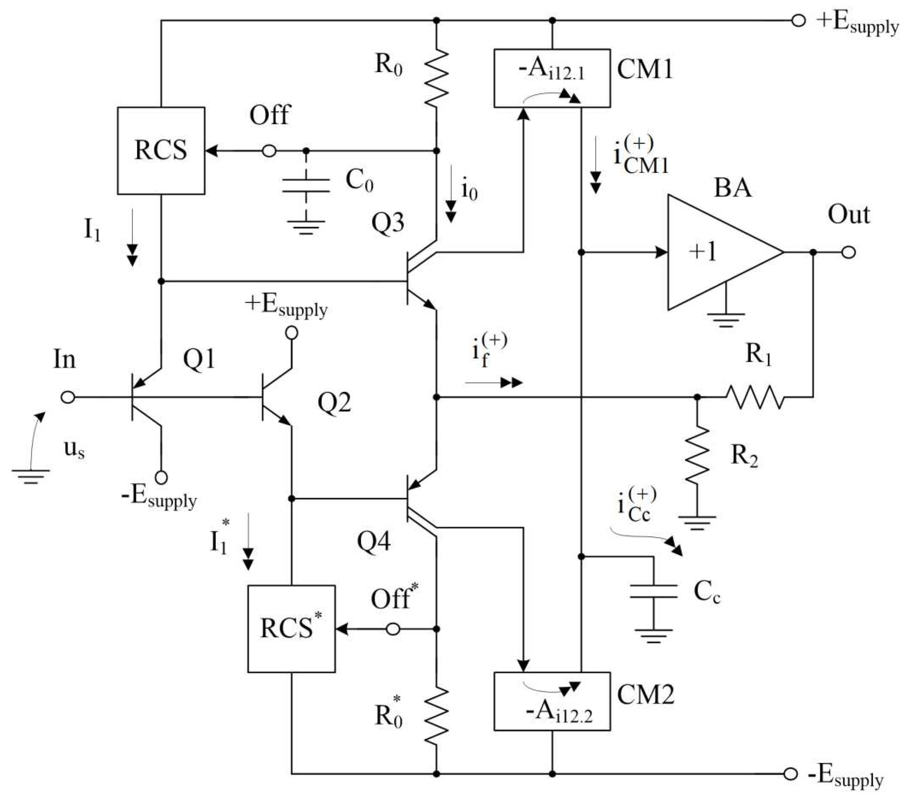
Figure 1. Non-inverting circuit for switching on a classic high-speed Op-Amp with general negative feedback.
Preprints 90886 g001
Figure 3. Method for limiting the maximum output current of the input stage of an Op-Amp with current negative feedback.
Preprints 90886 g003
Figure 4. Method for limiting the output current of the quad-core input stage.
Preprints 90886 g004
Figure 5. Current protection in the bridge input stage of a high-speed Op-Amp.
Preprints 90886 g005
Figure 6. High-speed BJT Op-Amp [33] with a differentiating transient correction circuit (Cc1).
Preprints 90886 g006
Figure 7. Transient process of the leading edge of the Op-Amp in Figure 6 at different values of the capacitance of the differentiating capacitor Cc1 = 0/25/50 pF.
Preprints 90886 g007
Figure 8. Op-amp circuit with differentiating correction circuit Cc1 and its transient process at different values of Cc1.
Preprints 90886 g008
Disclaimer/Publisher’s Note: The statements, opinions and data contained in all publications are solely those of the individual author(s) and contributor(s) and not of MDPI and/or the editor(s). MDPI and/or the editor(s) disclaim responsibility for any injury to people or property resulting from any ideas, methods, instructions or products referred to in the content.
Copyright: This open access article is published under a Creative Commons CC BY 4.0 license, which permit the free download, distribution, and reuse, provided that the author and preprint are cited in any reuse.
Prerpints.org logo

Preprints.org is a free preprint server supported by MDPI in Basel, Switzerland.

Subscribe

© 2024 MDPI (Basel, Switzerland) unless otherwise stated