
Submitted:
17 October 2023
Posted:
18 October 2023
You are already at the latest version
Abstract
Intercalation of noble metals can produce giant Rashba-type spin-orbit splittings in graphene. The spin-orbit splitting more than 100 meV has not yet been achieved in graphene on a metallic or a semiconductor substrate. Here, we report the p-type graphene obtained by Pt intercalation of zero-layer graphene on SiC substrate. The spin splitting of ∼200 meV was observed at a wide range of binding energies. Comparing the results of theoretical studies of different models with the experimantal ones measured by spin-ARPES, XPS and STM methods, we came to the conclusion that inducing giant spin-orbit splitting requires not only a fairly close arrangement of graphene to Pt layer, but also the presence of graphene corrugation caused by non-flat Pt layer. This makes it possible to find a compromise between strong hybridization and increased spin-orbit interaction. In our case, this is achieved by forming Pt submonolayer ordered on a nanometer scale under graphene.
Keywords:
graphene
; spin-ARPES
; Rashba spin-orbit coupling
; spin-orbit splitting
; graphene on silicon carbide
; intercalation
1. Introduction
Induced spin-orbit coupling in graphene is still actively investigated topic since it opens a way to realize quantum Hall effects in graphene [1,2,3,4]. It is known that a strong spin–orbit coupling is a necessary condition for observing spin Hall effects, quantum anomalous Hall effect, spin galvanic effect, spin Edelstein effect, giant Rashba effect, spin-transfer and spin-orbit torque effects, spin interference effect, etc.
Giant Rashba splitting in graphene on Au monolayer was reported earlier in several experimental papers [5,6,7,8,9,10,11], and was clearly supported by the density functional theory (DFT) calculations of Gr/Ni system with intercalated Au clusters [9] and tight-binding calculations of graphene on top of a gold monolayer in the hcp configuration [12]. The giant spin splitting was observed for Au-intercalated graphene on SiC substrate [8], but authors concluded that sizable spin splittings become giant (∼100 meV) only near avoided-crossing gap.
At the same time, platinum is the most used nonmagnetic metal in spintronics because it is characterized by spin-polarized states at the Fermi level, resulting in a high intrinsic spin Hall effect [13]. Furthermore, it was shown that graphene monolayer on Pt(111) surface [7] and on Ir(111) with intercalated Pt monolayer between graphene and Ir [14] exhibits pronounced spin-polarized Dirac cone-like states.
However, the systems of graphene on metal substrates cannot be directly applied for future electronics or spintronics. In this regards, graphene systems on semiconductor substrates, such as graphene on silicon carbide (SiC) with intercalated metal, are more promising for applications [15,16,17,18,19,20]. The possibility of intercalation of monolayer of noble metals underneath a graphene on SiC, such as Au and Pt, was shown in Refs. [8,16,17,21]. Also, in the work [22] it was predicted that in a system graphene/Pt/SiC with nanodots of ferromagnetic metals atop it, a reversible magnetization of ferromagnetic nanodots can be realized by applying a spin-current due to spin-orbit torque effect.
It is known that high temperature annealing of 6H-SiC(0001) surface leads to formation of ° reconstruction. Wherein, carbon layer at the surface is strongly bonded to the substrate and is called a zero-layer graphene (ZLG) [23,24,25]. Intercalation of various metals is a widely used method for transformation of zero-layer to quasi-freestanding graphene monolayer [21,26,27].
In the current work, we synthesize graphene system on SiC substrate with intercalated Pt submonolayer to evaluate the influence of corrugation at nanoscale on induced spin-orbit coupling in graphene. For this purpose intercalation of Pt atoms underneath ZLG was carried out. In contrast to the intercalation of 0.5 ML Au [9], a single ordered phase of graphene on Pt was achieved with a low atomic density in Pt monolayer. This made it possible to combine different research methods and interpret the results within single-phase system.
2. Materials and Methods
Synthesis and photoemission experiments were carried out in situ in ultra-high vacuum conditions in the setup Nanolab at the Resource Center “Physical Methods of Surface Investigation” of Saint Petersburg State University Research park. The samples were investigated by X-ray photoelectron spectroscopy (XPS), angle-resolved photoelectron spectroscopy (ARPES) using a VG Scienta R4000 hemispherical energy analyzer with spin Mott detector. A narrow-band high-intensity source of ultraviolet radiation VUV 5k and an X-ray radiation source with an Al anode with monochromators were used as excitation sources. The photoelectron spectra of the core levels were decomposed into spectral components by fitting procedure. The line shape of Si 2p and C 1s spectra was defined by Gaussian/Lorentzian product formula with mixing parameters of 0 and 0.5, respectively [28]. The asymmetry parameter for the graphene peak of C 1s spectra was 0.12. Raw data are shown in figures by circles along with the best-fit spectra, the corresponding components and the background. For analysis of crystalline and atomic structure we used low-energy electron diffraction (LEED) and scanning tunneling microscopy (STM).
Semi-insulating wafers of 6H-SiC(0001) purchased from TankeBlue Semiconductor Co. Ltd. (part number W26S0P-CPF) were used in the experiment. We provided deposition of 1.5 Å of Pt on the pristine surface of SiC(0001) with zero-layer graphene on top, and then the system was annealed at during 1 hour. The amount of deposited Pt was controlled by a quartz microbalance. The sample temperature was determined using Keller CellaTemp PA 20 AF 2/C pyrometer with the emissivity set to 0.6 for 60° off-normal angle. The base pressure was below mbar during the experiment.
First-principles calculations were performed using the OpenMX code which provides a fully relativistic DFT implementation with localized pseudoatomic orbitals [29,30] and norm-conserving pseudopotentials [31]. The exchange correlation energy in the PBE version of generalized gradient approximation was employed [32]. The accuracy of the real-space numerical integration was specified by the cutoff energy of 300 Ry, the total energy convergence criterion was 3·10−5 eV. The k-mesh for Brillouin zones of and supercells were specified as mesh. The basis functions were taken as C6.0–s2p2d1 and Pt7.0–s3p2d2f1 (the pseudopotential cutoff radius is followed by a basis set specification). The interfaces were modeled by periodic slabs consisting of one Pt atomic layer covered by graphene monolayer. The unit cell drawings were produced by VESTA software [33].
3. Results and discussion
Firstly, zero-layer graphene on SiC(0001) was synthesized at the temperature of about . Figure 1 shows the C 1s and Si 2p core levels spectra before and after Pt intercalation. Deconvolution of the photoelectron spectra into components by a fitting procedure is presented. The C 1s spectrum of ZLG (Figure 1(a)) has a characteristic shape with three components: two components S1 (284.7 eV) and S2 (285.5 eV), corresponding to the carbon in ZLG, and the component of bulk carbon (denoted by (B)) in the SiC compound (283.8 eV). The Si 2p spectrum (Figure 1(b)) presents one broad peak at the binding energy of 101.7 eV which is in accordance with the previous results [23,34,35]. However, the Si spin-orbit coupling doublet ( and ) is not resolved, so the one asymmetric peak is obtained during the fitting procedure. It should be noted that initial ZLG is assisted by a small amount of graphene monolayer (see a low-intensity component at 284.6 eV in Fig.1(a)). But as we will show below, this part of the surface is inert to intercalation process.
After Pt deposition and subsequent annealing at we observed the changes of the XPS spectra. First of all, they are followed by decreasing of the ZLG components and bulk component of carbon atoms in the SiC and increasing of the graphene component at 284.4 eV of binding energies. That means the transformation of ZLG into graphene monolayer by intercalation process. Secondly, the spectral components corresponding to Si and C atoms in the bulk SiC are both shifted by 0.9 eV towards lower binding energies. This effect can be explained by different surface band bending in the system due to the Pt atoms influence on the interface [36].
In order to study the depth location of underlying layers, it is necessary to carry out additional analysis of the XPS data with angular resolution, in which photoelectron spectra are taken at different emission angles. Analyzing the angular dependences of XPS core level intensities of the elements, it is possible to determine the relative positions of the layers in depth (see for example supplemental material of Ref. [37]). Figure 2 shows the changes of the C 1s, Pt 4f and Si 2p spectra measured at photoemission angles of 0° and 60° relative to the surface normal. The intensity ratios of the selected components for these two angles give us an understanding of the relative depth location. A more surface-sensitive spectrum corresponds to a larger photoemission angle. Therefore, comparing the intensity ratios for the C 1s graphene component, Pt 4f components and Si 2p bulk component (the numerical values of the ratios are shown in the Figure 2), we conclude that graphene is located above the Pt submonolayer, while the latter is localized between graphene and SiC substrate. It proves the intercalation of Pt underneath ZLG on SiC.
LEED image in Figure 3(a) shows formation of ZLG on SiC with () and () reconstructions [38]. Blurred moire pattern of graphene appeares after Pt intercalation (Figure 3(b)). ZLG reconstruction is no more visible proving intercalation of Pt atoms between ZLG and SiC substrate. Observation of SiC () diffraction spots up to high kinetic energies ( eV) evidences about good crystal quality of the substrate after intercalation. Notably, the measured period of superstructure ( nm nm) by STM method perfectly agrees with predicted one for 0° rotation angle between graphene and Pt layer [39].
To analyse the electronic structure of the system the ARPES intensity maps were measured before and after Pt deposition (Figure 3(c-f)). Due to the fact that the electronic structure of ZLG does not have intense electronic states near the Fermi level, even a small amount of graphene layer will contribute to the signal in ARPES spectra. As the result, the initial surface was characterized by presence of the graphene Dirac cone typical for graphene on SiC with n-doping and the Dirac point energy position at about 0.42 eV below the Fermi level (see Figure 3(d)) [23]. However, the graphene coverage was much less than ZLG one according to XPS data analysis.
After Pt intercalation a new Dirac cone is clearly visible on ARPES data in Figure 3(e,f). This cone is related to the intercalated graphene monolayer that was formed by ZLG transformation. It is shifted above the Fermi level (p-doping) due to Pt intercalation. At the same time, the initial Dirac cone remains unchanged. The band structure in the direction is shown in Figure 3(c). The and graphene states are observed, and Pt bands are slightly visible near the Fermi level.
Spin structure of intercalated graphene system was measured by spin-ARPES at k‖ values marked by blue arrows in Figure 3(c). The spin-resolved photoemission spectra are shown in Figure 4 for the in-plane Rashba spin component (Sy). The spin splitting of 200 meV (±50 meV) is observed for all measured spectra in the wide range of the binding energies. Such experimentally discovered value of spin splitting is unprecedentely giant for graphene systems and we will provide an explanation for this effect.
STM measurements were performed to provide more information about atomic structure of the surface. Only one well-ordered structure at large nanometer scales has been resolved, namely the structure of periodic triangular shaped defects (Figure 5). The periodicity of the superstructure is ∼(5×5) relative to graphene lattice. 2D fast Fourier transform (2D FFT) image shown on the inset of panel (b) also reveals the superstructure spots. Notably, a corrugation of about 0.2–0.3 Å was measured by STM, which is in a good agreement with the value reported for graphene on Pt(111) surface with vacancies in the topmost layer [37,40]. The observation of corrugation of a comparable magnitude after intercalation of an incomplete Pt monolayer is evidence that a rarefied platinum layer with holes is formed under graphene. In order to show the presence of a corrugated graphene lattice, we performed 2D FFT filtering of the image and presented it in a 3D view with illumination. The 2D-FFT image displays six spots corresponding to the superstructure, while the graphene structure is visible in the 3D image.
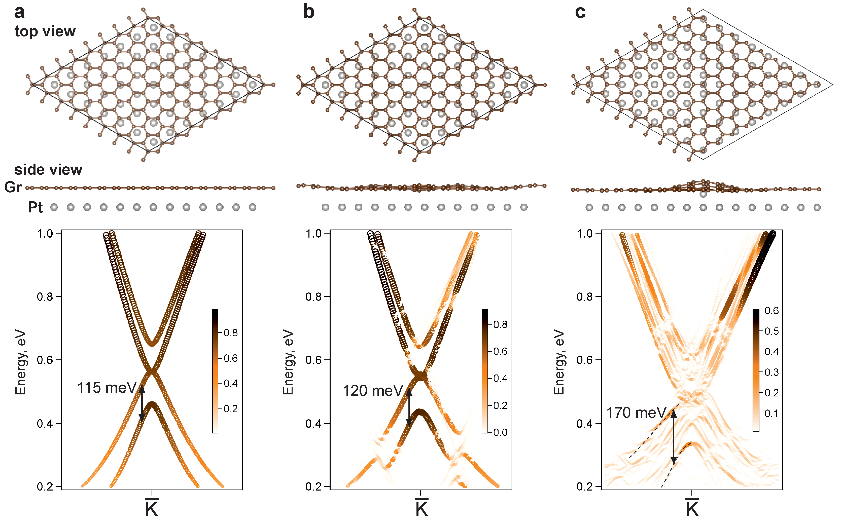
To analyze the causes of giant Rashba spin-orbit coupling phenomena and interpret obtained experimental data, we address to DFT calculations. In this regard, it should be noted that we were unable to find published information about experimental spin-orbit splittings in graphene with the energies above 100 meV. Similar experimental splitting values were obtained earlier, but only as a result of the interplay between exchange and spin-orbit couplings [10,11]. Moreover, DFT calculations had significant differences with the experimental results either in the magnitude of the spin-orbit splitting or in the atomic structure of graphene and the underlying layer. Due to impossibility to take into account all peculiarities of the real system structure in calculations and necessity to achieve experimental values of the spin splitting, unrealistic surface models are usually used. In our case of single-phase system, we have opportunity to provide the calculations of rather realistic simple model unit cells that might shed some light on the complex origin of the observed giant Rashba phenomenon. Single-phase system with a rarefied Pt layer with voids makes it possible to theoretically simplify the system as if it were intercalated by single Pt atoms. The first one is a model of Gr/Pt interface with flat layers (Figure 6(a)). The splitting close to 100 meV was obtained at a distance of ∼2.8 Å that is less than equilibrium distance for Gr/Pt(111) system (∼3.3-3.4 Å) [37,41]. But even such a close distance is not enough to obtain a splitting value which is comparable with the experimental one. It’s worth considering that further approchement of graphene and Pt layer leads not only to an increase in the splitting, but also to the destruction of the Dirac cone due to strong hybridization with Pt 5d states. In the second model, we check the influence of graphene corrugation near the average Gr-Pt distance of ∼2.8 Å . The graphene corrugation was obtained after structure optimization of Gr(8×8)/Pt interface with the equilibrium distance of ∼3.3 Å. Since the splitting increased slightly compared to the previous case, even though the carbon atoms now have different distances to the Pt layer, we can conclude that the average distance between graphene and Pt layer and the number of Pt atoms play a major role. In order to reduce this average distance without bringing the entire graphene and platinum closer together, we made a point defect in the form of an additional Pt atom under graphene and provide structural optimization of this system. In this case due to the formation of a "hat-like" structure in graphene above this Pt atom, some of carbon atoms have a very small distance to the nearest platinum atom (∼2.3 Å), which should increase the spin-orbit coupling induced in graphene. Besides, it should be noted that the structural optimization leads to the fact that the flat areas became even closer to the Pt layer (∼2.5 Å). As it turned out, such a defect enhanced the splitting to a value ∼170 meV. Notably, graphene Dirac dispersion is not destroyed. Within the experimental resolution we have a good agreement between this model and the experiment. Thus, important features revealed for the first time in the calculations are: the possibility of graphene corrugation in a large-scale unit cell with a flat substrate and graphene pinning effect in case of point defects in the form of Pt atoms under graphene.
Without any doubt, the unit cells used in calculations have too small lateral parameters and a model of the system based on STM data should have an unit cell with minimal dimensions (15x15) with a periodic arrangement of voids and a quasi-periodic arrangement of Pt atoms between them. For this reason our DFT calculations cannot fully take into account the complex structure of the real surface and a challenging task of large unit cells calculations should be solved to establish completely the role of nanometer-scale unit cells in giant Rashba effect. However, despite the described limitations, we believe that the performed calculations of model unit cells give a good enough idea of the possible cause of the giant Rashba splitting in the considered system, which consists in reduction of the average distance between carbon and platinum atoms due to the appearance of an ordered network of platinum clusters and voids under graphene.
4. Conclusions
Our study of Pt-intercalated graphene on SiC substrate revealed an ordered single-phase consisting of graphene on rarefied Pt layer with triangular-shaped voids. Corrugated graphene on such Pt layer has a giant spin splitting value of about 200 meV. Theoretical model with additional platinum atoms under graphene shows a decrease in the distance between graphene and Pt layer atoms as a result of the pinning effect and the corrugation of graphene at the sites of point defects. It is supposed that a more complex interface between graphene and intercalated noble metal layer with pinning defects underlies the giant Rashba effect.
Author Contributions
Conceptualization, A.A.R. and A.G.R.; methodology, A.A.R., A.A.G., A.V.T., V.Yu.V., I.I.K. and A.G.R.; software, A.A.G. and A.V.T.; validation, A.A.R., A.V.T., A.G.R.; formal analysis, A.A.R., A.A.G., A.V.T., Y.X. and V.Yu.V.; investigation, A.A.R., A.A.G., A.V.T., Y.X., V.Yu.V, D.A.P., I.I.K., A.E.P., K.A.B. and A.G.R.; resources, A.A.R, A.V.T, D.A.P. and A.E.P.; data curation, A.A.R., A.A.G., A.V.T., Y.X. and A.G.R.; writing—original draft preparation, A.A.R., A.V.T., Y.X., V.Yu.V. and A.G.R.; writing—review and editing, all authors; visualization, A.A.R., A.A.G, A.V.T. and A.G.R.; supervision, C.Y., Z.Z. and A.M.S.; project administration, A.G.R.; funding acquisition, A.M.S. All authors have read and agreed to the published version of the manuscript.
Funding
This research was funded by Ministry of Science and Higher Education of the Russian Federation grant number 075-15-2020-797 (13.1902.21.0024).
Acknowledgments
We thank Resource Center “Physical Methods of Surface Investigation” of Saint Petersburg State University for providing the opportunity to perform the experiment. The calculations were partially performed using the equipment of the Joint Supercomputer Center of the Russian Academy of Sciences (https://rscgroup.ru/en/project/jscc). The authors thank A.V. Eryzhenkov for providing possibility of calculations using his band unfolding code.
Conflicts of Interest
The authors declare no conflict of interest.
References
- Kane, C.L.; Mele, E.J. Z2 Topological Order and the Quantum Spin Hall Effect. Phys. Rev. Lett. 2005, 95, 146802. [CrossRef]
- Phong, V.T.; Walet, N.R.; Guinea, F. Effective interactions in a graphene layer induced by the proximity to a ferromagnet. 2D Materials 2017, 5, 014004. [CrossRef]
- Eryzhenkov, A.V.; Tarasov, A.V.; Shikin, A.M.; Rybkin, A.G. Non-Trivial Band Topology Criteria for Magneto-Spin-Orbit Graphene. Symmetry 2023, 15. [CrossRef]
- Chen, L.; Li, F.; Ding, X.M. Rashba spin–orbit coupling induced rectified currents in monolayer graphene with exchange field and sublattice potential. Chinese Physics B 2023, 32, 087103. [CrossRef]
- Shikin, A.M.; Rybkin, A.G.; Marchenko, D.; Rybkina, A.A.; Scholz, M.R.; Rader, O.; Varykhalov, A. Induced spin–orbit splitting in graphene: the role of atomic number of the intercalated metal and pi–d hybridization. New Journal of Physics 2013, 15, 013016. [CrossRef]
- Marchenko, D.; Varykhalov, A.; Scholz, M.R.; Bihlmayer, G.; Rashba, E.I.; Rybkin, A.; Shikin, A.M.; Rader, O. Giant Rashba splitting in graphene due to hybridization with gold. Nature Communications 2012, 3, 1232, [1208.4265]. [CrossRef]
- Klimovskikh, I.I.; Tsirkin, S.S.; Rybkin, A.G.; Rybkina, A.A.; Filianina, M.V.; Zhizhin, E.V.; Chulkov, E.V.; Shikin, A.M. Nontrivial spin structure of graphene on Pt(111) at the Fermi level due to spin-dependent hybridization. Physical Review B 2014, 90, 1–10. [CrossRef]
- Marchenko, D.; Varykhalov, A.; Sánchez-Barriga, J.; Seyller, T.; Rader, O. Rashba splitting of 100 meV in Au-intercalated graphene on SiC. Applied Physics Letters 2016, 108, 172405, [https://pubs.aip.org/aip/apl/article-pdf/doi/10.1063/1.4947286/14478504/172405_1_online.pdf]. [CrossRef]
- Krivenkov, M.; Golias, E.; Marchenko, D.; Sánchez-Barriga, J.; Bihlmayer, G.; Rader, O.; Varykhalov, A. Nanostructural origin of giant Rashba effect in intercalated graphene. 2D Materials 2017, 4, 035010. [CrossRef]
- Rybkin, A.G.; Rybkina, A.A.; Otrokov, M.M.; Vilkov, O.Y.; Klimovskikh, I.I.; Petukhov, A.E.; Filianina, M.V.; Voroshnin, V.Y.; Rusinov, I.P.; Ernst, A.; Arnau, A.; Chulkov, E.V.; Shikin, A.M. Magneto-Spin–Orbit Graphene: Interplay between Exchange and Spin–Orbit Couplings. Nano Letters 2018, 18, 1564–1574. [CrossRef]
- Rybkin, A.G.; Tarasov, A.V.; Rybkina, A.A.; Usachov, D.Y.; Petukhov, A.E.; Eryzhenkov, A.V.; Pudikov, D.A.; Gogina, A.A.; Klimovskikh, I.I.; Di Santo, G.; Petaccia, L.; Varykhalov, A.; Shikin, A.M. Sublattice Ferrimagnetism in Quasifreestanding Graphene. Phys. Rev. Lett. 2022, 129, 226401. [CrossRef]
- López, A.; Colmenárez, L.; Peralta, M.; Mireles, F.; Medina, E. Proximity-induced spin-orbit effects in graphene on Au. Phys. Rev. B 2019, 99, 085411. [CrossRef]
- Guo, G.Y.; Murakami, S.; Chen, T.W.; Nagaosa, N. Intrinsic Spin Hall Effect in Platinum: First-Principles Calculations. Physical Review Letters 2008, 100, 096401. [CrossRef]
- Klimovskikh, I.I.; Vilkov, O.; Usachov, D.Y.; Rybkin, A.G.; Tsirkin, S.S.; Filianina, M.V.; Bokai, K.; Chulkov, E.V.; Shikin, A.M. Variation of the character of spin-orbit interaction by Pt intercalation underneath graphene on Ir(111). Phys. Rev. B 2015, 92, 165402. [CrossRef]
- Briggs, N.; Gebeyehu, Z.M.; Vera, A.; Zhao, T.; Wang, K.; De La Fuente Duran, A.; Bersch, B.; Bowen, T.; Knappenberger, K.L.; Robinson, J.A. Epitaxial graphene/silicon carbide intercalation: a minireview on graphene modulation and unique 2D materials. Nanoscale 2019, 11, 15440–15447. [CrossRef]
- Xia, C.; Johansson, L.I.; Niu, Y.; Zakharov, A.a.; Janzén, E.; Virojanadara, C. High thermal stability quasi-free-standing bilayer graphene formed on 4H-SiC(0001) via platinum intercalation. Carbon 2014, 79, 631–635. [CrossRef]
- Premlal, B.; Cranney, M.; Vonau, F.; Aubel, D.; Casterman, D.; De Souza, M.M.; Simon, L. Surface intercalation of gold underneath a graphene monolayer on SiC(0001) studied by scanning tunneling microscopy and spectroscopy. Applied Physics Letters 2009, 94, 1–4. [CrossRef]
- Yagyu, K.; Tajiri, T.; Kohno, A.; Takahashi, K.; Tochihara, H.; Tomokage, H.; Suzuki, T. Fabrication of a single layer graphene by copper intercalation on a SiC(0001) surface. Applied Physics Letters 2014, 104, 053115. [CrossRef]
- Sung, S.J.; Yang, J.W.; Lee, P.R.; Kim, J.G.; Ryu, M.T.; Park, H.M.; Lee, G.; Hwang, C.C.; Kim, K.S.; Kim, J.S.; Chung, J.W. Spin-induced band modifications of graphene through intercalation of magnetic iron atoms. Nanoscale 2014, 6, 3824. [CrossRef]
- Yang, D.; Xia, Q.; Gao, H.; Dong, S.; Zhao, G.; Zeng, Y.; Ma, F.; Hu, T. Fabrication and mechanism of Pb-intercalated graphene on SiC. Applied Surface Science 2021, 569, 151012. [CrossRef]
- Gierz, I.; Suzuki, T.; Weitz, R.T.; Lee, D.S.; Krauss, B.; Riedl, C.; Starke, U.; Höchst, H.; Smet, J.H.; Ast, C.R.; Kern, K. Electronic decoupling of an epitaxial graphene monolayer by gold intercalation. Physical Review B 2010, 81, 235408. [CrossRef]
- Shikin, A.M.; Rybkina, A.A.; Rybkin, A.G.; Klimovskikh, I.I.; Skirdkov, P.N.; Zvezdin, K.A.; Zvezdin, A.K. Spin current formation at the graphene/Pt interface for magnetization manipulation in magnetic nanodots. Applied Physics Letters 2014, 105, 042407. [CrossRef]
- Riedl, C.; Coletti, C.; Starke, U. Structural and electronic properties of epitaxial graphene on SiC (0 0 0 1): a review of growth, characterization, transfer doping and hydrogen intercalation. Journal of Physics D: Applied Physics 2010, 43, 374009. [CrossRef]
- Riedl, C.; Coletti, C.; Iwasaki, T.; Zakharov, A.A.; Starke, U. Quasi-free-standing epitaxial graphene on SiC obtained by hydrogen intercalation. Physical Review Letters 2009, 103, 1–4, [arXiv:0911.1953v1]. [CrossRef]
- Emtsev, K.V.; Speck, F.; Seyller, T.; Ley, L.; Riley, J.D. Interaction, growth, and ordering of epitaxial graphene on SiC{0001} surfaces: A comparative photoelectron spectroscopy study. Physical Review B - Condensed Matter and Materials Physics 2008, 77, 1–10. [CrossRef]
- Rybkina, A.A.; Filnov, S.O.; Tarasov, A.V.; Danilov, D.V.; Likholetova, M.V.; Voroshnin, V.Y.; Pudikov, D.A.; Glazkova, D.A.; Eryzhenkov, A.V.; Eliseyev, I.A.; Davydov, V.Y.; Shikin, A.M.; Rybkin, A.G. Quasi-freestanding graphene on SiC(0001) via cobalt intercalation of zero-layer graphene. Phys. Rev. B 2021, 104, 155423. [CrossRef]
- Sohn, Y.; Shin, W.; Ryu, S.; Huh, M.; Cha, S.; Kim, K. Graphene p-n junction formed on SiC(0001) by Au intercalation. Journal of the Korean Physical Society 2021, 78, 40. [CrossRef]
- Jain, V.; Biesinger, M.C.; Linford, M.R. The Gaussian-Lorentzian Sum, Product, and Convolution (Voigt) functions in the context of peak fitting X-ray photoelectron spectroscopy (XPS) narrow scans. Applied Surface Science 2018, 447, 548–553. [CrossRef]
- Ozaki, T. Variationally optimized atomic orbitals for large-scale electronic structures. Phys. Rev. B 2003, 67, 155108. [CrossRef]
- Ozaki, T.; Kino, H. Numerical atomic basis orbitals from H to Kr. Phys. Rev. B 2004, 69, 195113. [CrossRef]
- Troullier, N.; Martins, J.L. Efficient pseudopotentials for plane-wave calculations. Physical review B 1991, 43, 1993. [CrossRef]
- Perdew, J.P.; Wang, Y. Accurate and simple analytic representation of the electron-gas correlation energy. Phys. Rev. B 1992, 45, 13244–13249. [CrossRef]
- Momma, K.; Izumi, F. VESTA3 for three-dimensional visualization of crystal, volumetric and morphology data. Journal of Applied Crystallography 2011, 44, 1272–1276. [CrossRef]
- Merino, P. Dissertation “Structural characterization of epitaxial graphene”; Universidad Autónoma de Madrid, 2014.
- Emtsev, K. Dissertation “Electronic and structural characterizations of unreconstructed SiC(0001) surfaces and the growth of graphene overlayers”; Friedrich-Alexander-Universität Erlangen-Nürnberg, 2009.
- Tedesco, J.L.; Rowe, J.E.; Nemanich, R.J. Conducting atomic force microscopy studies of nanoscale cobalt silicide Schottky barriers on Si(111) and Si(100). Journal of Applied Physics 2009, 105, 083721. [CrossRef]
- Rybkin, A.G.; Rybkina, A.A.; Tarasov, A.V.; Pudikov, D.A.; Klimovskikh, I.I.; Vilkov, O.Y.; Petukhov, A.E.; Usachov, D.Y.; Estyunin, D.A.; Voroshnin, V.Y.; Varykhalov, A.; Di Santo, G.; Petaccia, L.; Schwier, E.F.; Shimada, K.; Kimura, A.; Shikin, A.M. A new approach for synthesis of epitaxial nano-thin Pt5Gd alloy via intercalation underneath a graphene. Applied Surface Science 2020, 526, 146687. [CrossRef]
- Riedl, C.; Starke, U.; Bernhardt, J.; Franke, M.; Heinz, K. Structural properties of the graphene-SiC(0001) interface as a key for the preparation of homogeneous large-terrace graphene surfaces. Phys. Rev. B 2007, 76, 245406. [CrossRef]
- Merino, P.; Sv̌ec, M.; Pinardi, A.L.; Otero, G.; Martín-Gago, J.A. Strain-Driven Moiré Superstructures of Epitaxial Graphene on Transition Metal Surfaces. ACS Nano 2011, 5, 5627–5634. [CrossRef]
- Otero, G.; González, C.; Pinardi, A.L.; Merino, P.; Gardonio, S.; Lizzit, S.; Blanco-Rey, M.; Van de Ruit, K.; Flipse, C.F.J.; Méndez, J.; de Andrés, P.L.; Martín-Gago, J.A. Ordered Vacancy Network Induced by the Growth of Epitaxial Graphene on Pt(111). Phys. Rev. Lett. 2010, 105, 216102. [CrossRef]
- Wang, Q.; Pang, R.; Shi, X. Molecular Precursor Induced Surface Reconstruction at Graphene/Pt(111) Interfaces. The Journal of Physical Chemistry C 2015, 119, 22534–22541. [CrossRef]
Figure 1.
XPS spectra of C 1s (a) and Si 2p (b) core levels measured for ZLG on SiC - bottom row, and after 1.5 Å Pt intercalation underneath ZLG on SiC - top row. The photon energy is 1486.6 eV.
Figure 1.
XPS spectra of C 1s (a) and Si 2p (b) core levels measured for ZLG on SiC - bottom row, and after 1.5 Å Pt intercalation underneath ZLG on SiC - top row. The photon energy is 1486.6 eV.
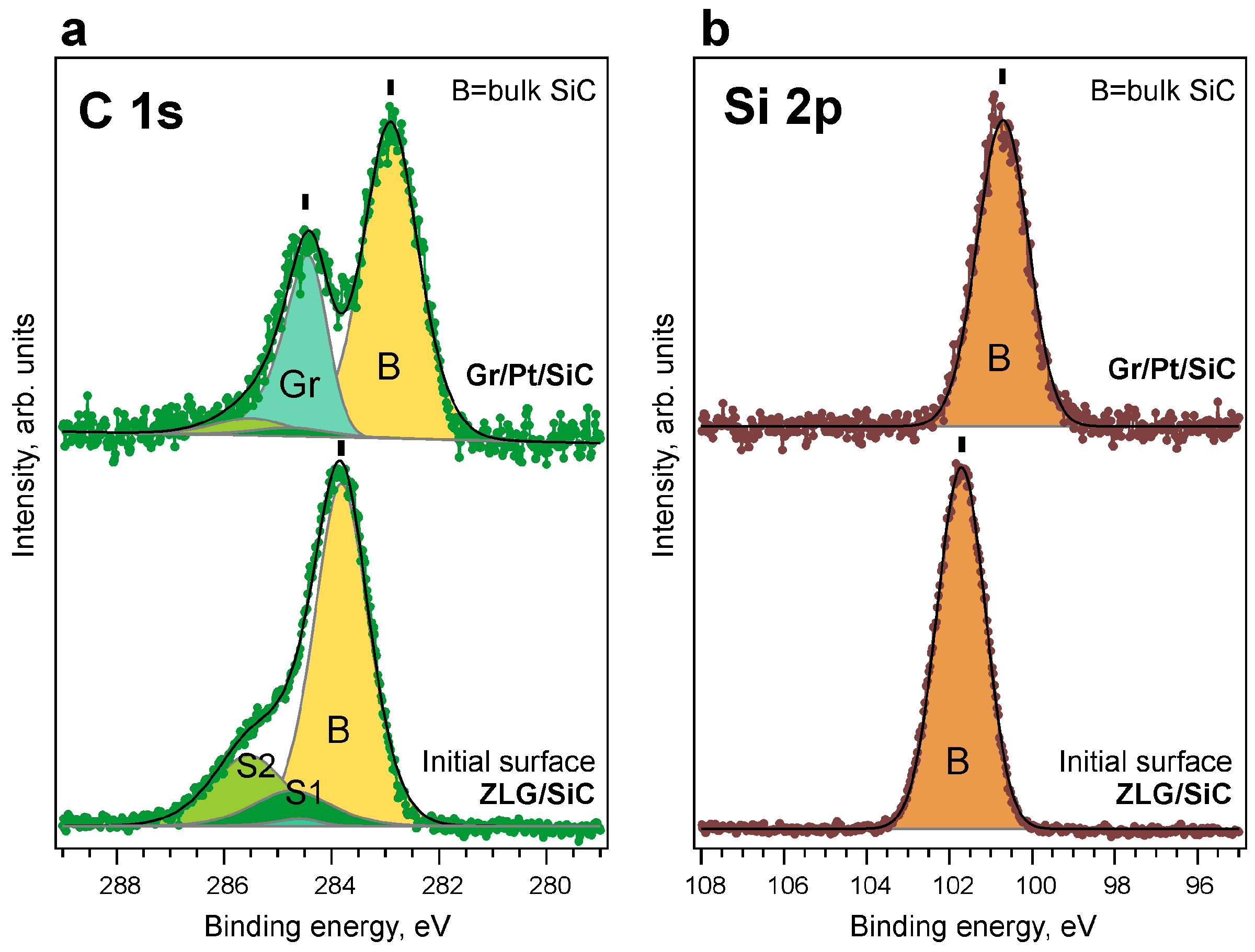
Figure 2.
Angle-resolved XPS spectra measured at emission angles of 0° and 60° relative to the surface normal for (a) - C 1s, (b) - Pt 4f, (c) - Si 2p core levels, after Pt intercalation underneath ZLG on SiC. The photon energy is 1486.6 eV.
Figure 2.
Angle-resolved XPS spectra measured at emission angles of 0° and 60° relative to the surface normal for (a) - C 1s, (b) - Pt 4f, (c) - Si 2p core levels, after Pt intercalation underneath ZLG on SiC. The photon energy is 1486.6 eV.
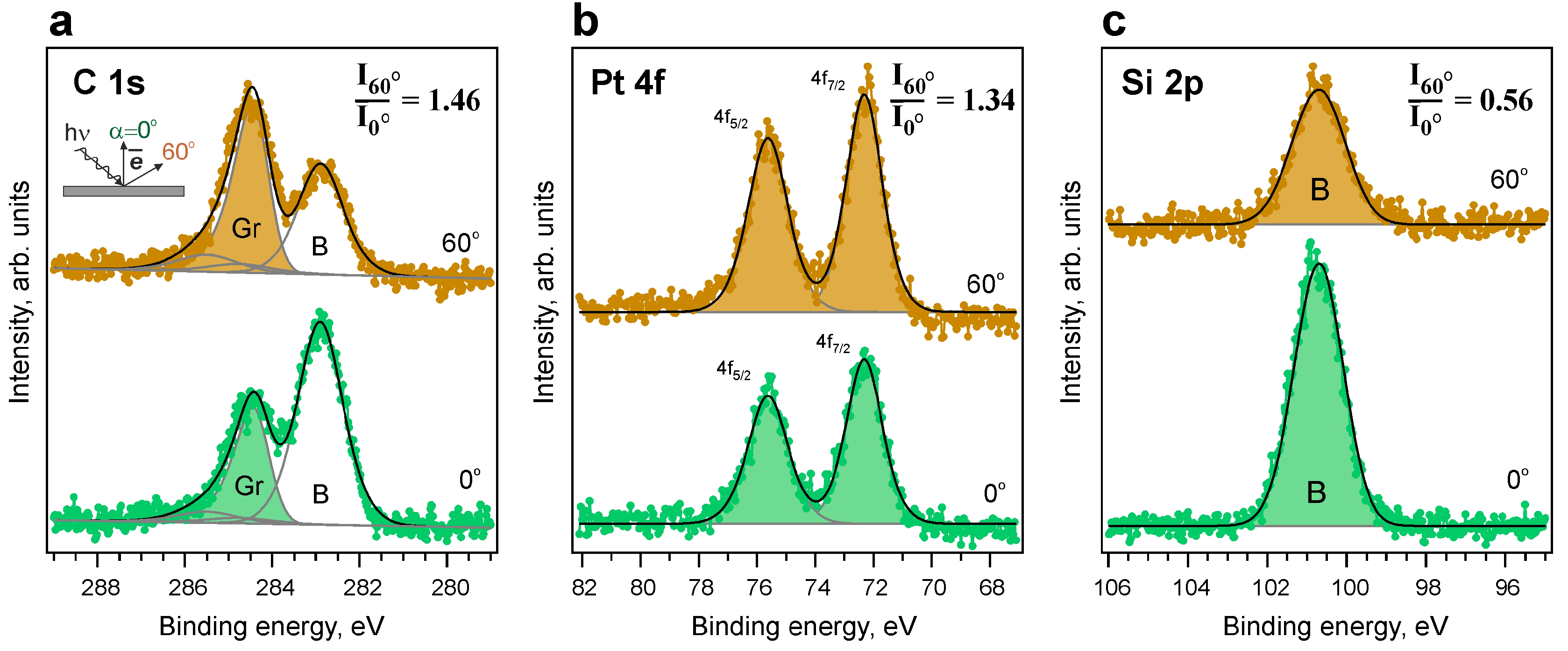
Figure 3.
(a), (b) - LEED patterns of the initial surface of R30° reconstruction of SiC surface (zero-layer graphene) with small amount of graphene monolayer and the surface after 1.5 Å Pt intercalation, Ep=100 eV. (c) - ARPES intensity maps of the surface after Pt intercalation measured along the direction of the surface Brillouin zone and presented as the second derivative by energy. (d), (e) - ARPES intensity maps of the initial surface and after Pt intercalation measured in the direction orthogonal to the . Solid red lines show the result of momentum distribution curves fitting with two Lorentzian peak functions. Enlarged view of the Dirac cone for the initial surface shown in the inset with inverted palette. (f) - ARPES data from (e) presented as the second derivative by energy to discern the main features more clearly. The photon energy is 40.8 eV (He II).
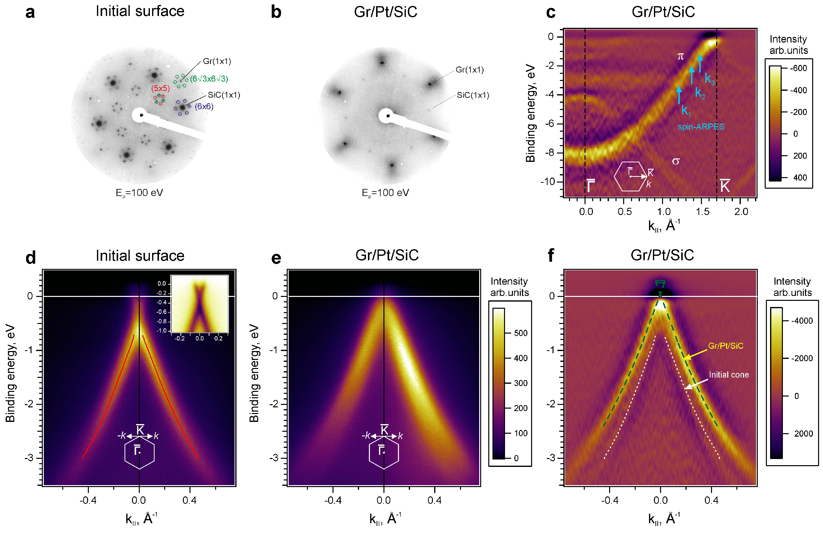
Figure 4.
Spin-ARPES spectra (a) with the spin polarizations (b) of Gr/Pt/SiC(0001) system measured at , and momenta in Figure 3 (c). The photon energy is 40.8 eV (He II).
Figure 4.
Spin-ARPES spectra (a) with the spin polarizations (b) of Gr/Pt/SiC(0001) system measured at , and momenta in Figure 3 (c). The photon energy is 40.8 eV (He II).
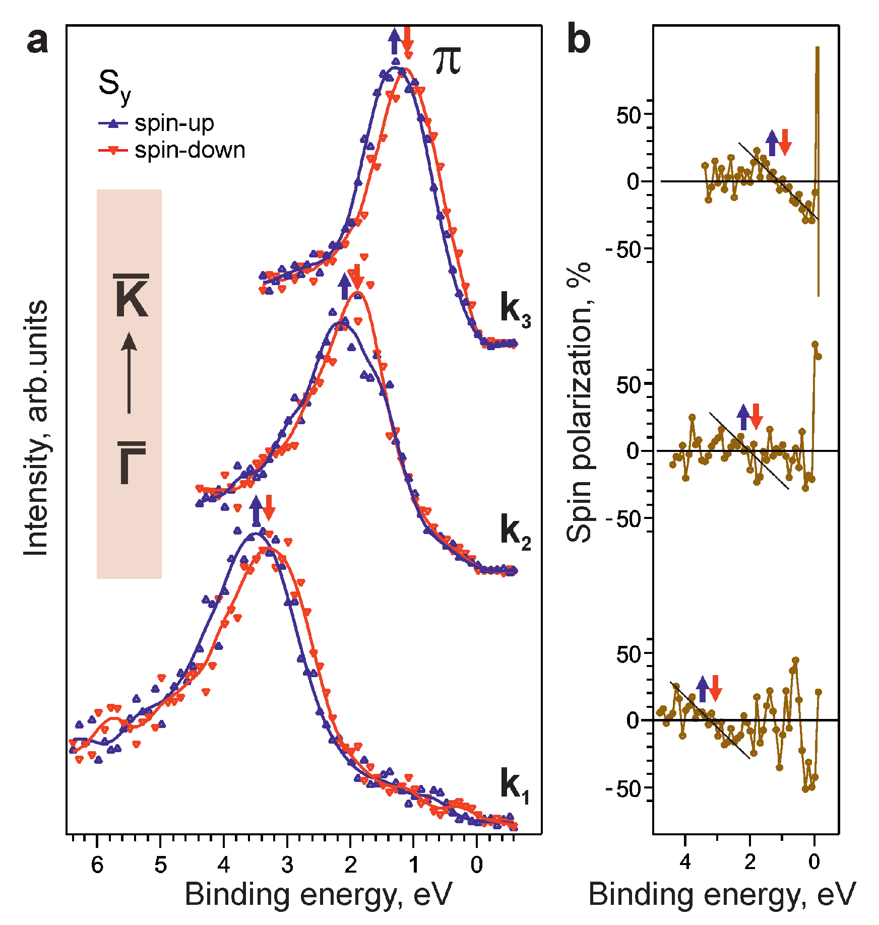
Figure 5.
STM images for the system graphene/Pt/SiC after annealing at temperature T=1100 °C. The image sizes and measurement parameters are as follows: (a) 30×30 nm, Vs=-0.4 V, It=0.5 nA, (b) 11 nm, Vs=-0.5 V, It=0.5 nA. A 2D FFT of the STM image is shown on the inset in panel (b). (c) 3D view of the image with 2D FFT filtering for graphene lattice visibility. Enlarged area is presented in the inset.
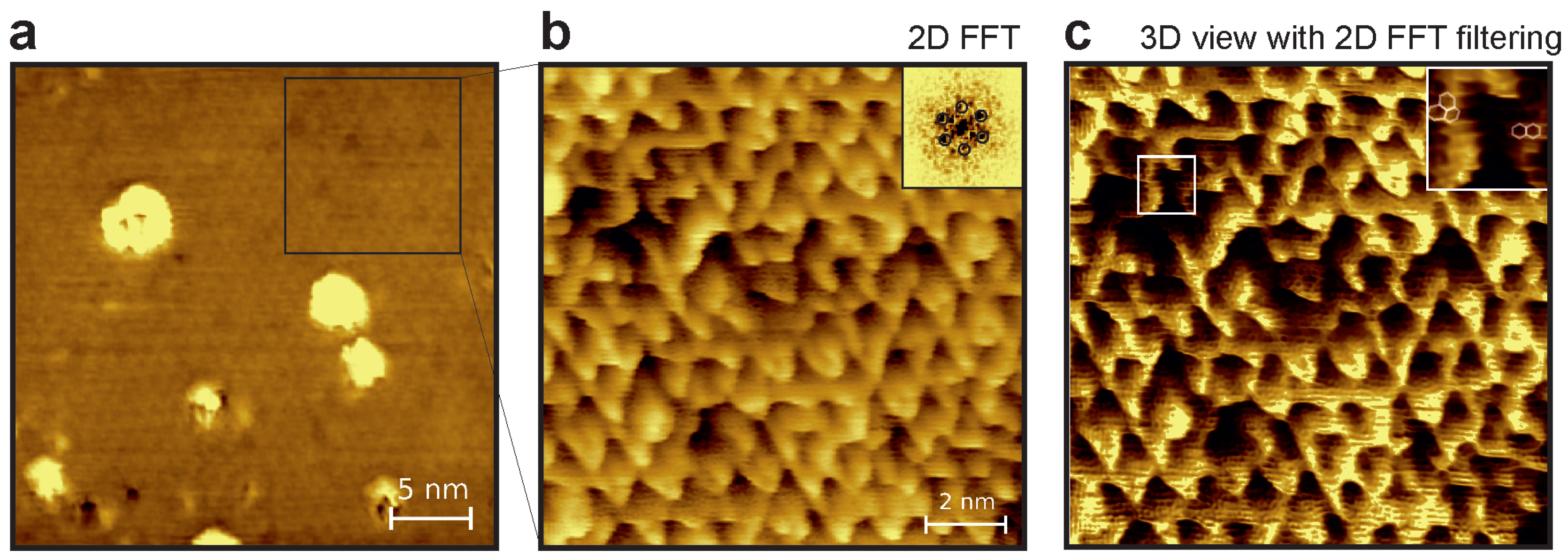
Figure 6.
The model slab systems of Gr/Pt interface: (8×8) with flat graphene and Pt layer (a), (8×8) with a large-scale graphene corrugation (b) and (9×9) with graphene corrugation induced by Pt atom (c). The corresponding DFT calculated unfolded bands near point along direction of graphene Brillouin zone are shown below. The symbol size and colour palette denote the Bloch spectral weight of carbon atoms for unfolded band structure.
Disclaimer/Publisher’s Note: The statements, opinions and data contained in all publications are solely those of the individual author(s) and contributor(s) and not of MDPI and/or the editor(s). MDPI and/or the editor(s) disclaim responsibility for any injury to people or property resulting from any ideas, methods, instructions or products referred to in the content. |
© 2023 by the authors. Licensee MDPI, Basel, Switzerland. This article is an open access article distributed under the terms and conditions of the Creative Commons Attribution (CC BY) license (http://creativecommons.org/licenses/by/4.0/).
Copyright: This open access article is published under a Creative Commons CC BY 4.0 license, which permit the free download, distribution, and reuse, provided that the author and preprint are cited in any reuse.


