
Submitted:
13 October 2023
Posted:
16 October 2023
You are already at the latest version
Abstract
The influence of various energetic particles and electron injection on transport of minority carriers and non-equilibrium carrier recombination in Ga2O3 is summarized in this review. In Ga2O3 semiconductor, if robust p-type material and bipolar structures become available, diffusion length of minority carriers will be of critical significance. Diffusion length of minority carriers dictates functionality of such electronic devices as diodes, transistors, and detectors. One of the problems in ultra-wide band gap materials technology, is the short carrier diffusion length, due to scattering on extended defects. Electron injection in n- and p-type Gallium Oxide results in a significant increase of the diffusion length, even after its deterioration due to exposure to alpha- and proton-irradiation. Furthermore, post electron injection diffusion length in irradiated material exceeds that in Ga2O3 prior to irradiation and injection. The root cause of the electron injection-induced effect is attributed to the increase of minority carrier lifetime in the material due to trapping of non-equilibrium electrons on native point defects. It is, therefore, concluded that the electron injection is capable of “healing” the adverse impact of radiation in Ga2O3 and can be used for control of minority carrier transport and, therefore, device performance.
Keywords:
Gallium Oxide
; transport properties
; minority carriers
1. Introduction
Semiconductors with wide band gap (WBG), among which Gallium Nitride and Zinc Oxide are the notable examples, are of significant relevance for high temperature electronics and solar-blind ultraviolet radiation detection in the hither cosmos [1,2,3]. The novel Gallium Oxide semiconductor with a direct forbidden gap of 4.7-4.9 eV (ultra-wide bandgap) is becoming promising for harsh environment applications in terms of its superior stability over GaN and ZnO counterparts [1,4,5,6,7,8,9].
At present, the major limitation in Gallium Oxide applications is manifested in difficulties related to hole conductivity [7,9,10,11,12]. It turns out that holes in β-Ga2O3 possess high effective mass, as well as low dispersion and high density of states. These factors dictate creation of self-trapped holes [13,14,15,16,17], hindering p-type conductivity. Contrasting to these claims, refs. [10,11] have reported a feasibility for hole conductivity at elevated temperatures for as grown beta Gallium Oxide. The findings in refs. [10,11] are in agreement with the results presented in ref. [12], showing that self-trapping nature of holes vanishes above 90-120 K [12]. Accounting for high interest in robust p-type doping in Gallium Oxide, it is expected that Gallium Oxide-based bipolar devices will soon become a reality.
In Ga2O3 semiconductor, if robust p-type material and bipolar structures become available, diffusion length of minority carriers will be of critical significance. Diffusion length dictates functionality of such electronic devices as diodes, transistors, and detectors [18]. One of the problems in wide band gap materials (Zinc Oxide and Gallium Nitride) technology, is the short carrier diffusion length, due to scattering on extended defects [19,20]. At the same time, low energy electron injection into p-type GaN and ZnO, using either an electron beam of Scanning Electron Microscope (SEM) or forward bias of Schottky barriers or p-n junctions, leads to drastic elongation of the minority electron diffusion length in these materials [19,21,22,23,24]. Similar effects were reported in n-type Ga2O3 using SEM electron beam or solid-state electron injection (see below and refs. [25,26]), and then in highly-resistive p-type material [27]. Diffusion length increase translated into changes in the luminescent characteristics of GaN, ZnO and Ga2O3 [26,28,29,30], and into experimentally demonstrated superior photovoltaic detector performance in the case of GaN and ZnO [18,24,31,32], and, very recently, in Ga2O3-based heterostructures.
It was also discovered that, on the one hand, irradiation of Si-doped β-Ga2O3 by 1.5 MeV electrons, 18 MeV α-particles or 10 MeV protons, leads to deterioration of minority carrier diffusion length and minority carrier lifetime [25,33,34,35]. On the other hand, low energy SEM beam injection into irradiated Ga2O3 Schottky barrier recovers/enhances minority carrier transport, as is expressed in consequent long-lasting diffusion length increase [25,26,27,35]. It should be stressed that the diffusion length in irradiated Gallium Oxide samples after electron injection surpasses that prior to irradiation and injection. It is, therefore, possible to use SEM beam (or forward bias) electron injection for improving material’s fundamental properties and, in prospective, performance of devices, which are dependent on minority carrier transport and affected by radiation.
2. The Outline for this Review is as follows
- Methodology for diffusion length measurements in-situ in Scanning Electron Microscope will be explained on the example of highly resistive p-Ga2O3.
- Methodology for electron beam probing of optical properties will be outlined using results for n-type Ga2O3, as an example.
- Impact of various radiation types on minority carrier transport and optical properties will be reviewed.
- Influence of SEM electron injection on minority carrier diffusion in Ga2O3 before and after exposure to radiation will be discussed.
- The root cause for the phenomenon of electron injection in Gallium Oxide and its impact on minority carrier transport will be explained.
- Application of the electron injection effect to photoresponse enhancement in Gallium Oxide-based heterostructures will be considered as an example.
- The main conclusions will be summarized.
2.1. Electron Beam-Induced Current Measurements of Minority Carrier Diffusion Length
Diffusion length of minority carriers was measured using Electron Beam-Induced Current (EBIC) technique in a Scanning Electron Microscope (SEM). The diffusion length was relevant for electrons or holes depending on electrical conductivity type. The measurements were carried out on Schottky contacts in the room temperature (RT) –130 oC range using a temperature-controlled stage installed in the SEM vacuum chamber. The electron beam accelerating voltage varied between 10 and 30 kV. The EBIC line-scans were recorded on a planar structure shown in Figure 1. The signal was amplified using a Stanford Research Systems SR 570 low-noise current amplifier and digitized with a Keithley 2000 multimeter, which was controlled using a homemade software.
Diffusion length, L, was extracted from the EBIC line-scans using the following equation [37,38,39]:
Here, C(x) is the Electron Beam-Induced Current signal as a function of coordinate; C0 is a scaling factor; x is the coordinate counted from the edge of the contact stack; α is a recombination coefficient (set at -0.5).
Figure 2 illustrates methodology for minority carrier diffusion length extraction on the example of two highly resistive p-type samples. Because of low carrier concentration in the structures under test, the metal/semiconductor space-charge region (cf. Figure 1) was comparable or wider than the diffusion length. Hence, the methodology explained in ref. [37] has been employed. Figure 2a,b demonstrate the raw data and their fit, using Equation 1, which was employed for extraction of L for two samples under test (samples A and B; A: p = 5.6 x 1014 cm−3; μ = 8.0 cm2V−1s−1; B: p = 2.7 x 1013 cm−3 and μ = 16 cm2V−1s−1). While majority hole concentration and mobility for the above-referenced samples were measured at 850 K using Hall effect setup, the EBIC testing was done at 300-400 K.
Minority carrier diffusion length dependence on temperature, T, for highly resistive p-type material is demonstrated in Figure 3. Decrease of L with rising T is a typical trend observed in Gallium Oxide. Large values of L in Figure 3 are an additional indirect proof for samples being p-type, as minority carriers in this case are electrons, which possess much higher mobility as compared to holes. The latter have a large effective mass of 18.8 m0 [43]. L for minority carriers in n-Gallium Oxide is in 50-600 nm range [25,26,33,41,42], which is much lower than that reported in ref. [36] for minority carrier electrons. Another reason for large values of the diffusion length in Figure 3 is related to the low majority carrier concentrations in the samples A and B and, therefore, low scattering on electrically active impurities. Phonon scattering [40] may also play a role. It should be noted that a dependence of L on temperature, similar to the one in Figure 3, was found for n-type β-Ga2O3, and was ascribed to ionized impurity scattering because of heavy Si doping [33].
Inset: Arrhenius plot and the fit for ΔEL,T. Reprinted with permission from the AIP. After ref. [36].
Here, L0 is a scaling constant; ΔEL,T is the thermal activation energy; k is the Boltzmann constant; and T is the temperature. The activation energy related to L decrease with temperature was found to be 67 meV (sample A) and 113 meV (samples B), respectively. The difference in the activation energies for the samples A and B is mainly because of the difference in their majority carrier concentrations, determined, in turn, by the partial pressure of oxygen, which was set during the epitaxial growth.
2.2. Continuous and Time-Resolved Cathodoluminescence
Cathodoluminescence (CL) is a powerful tool for measuring light emission from the material. It offers a greater spatial resolution in comparison to the photoluminescence (PL). The electron beam energy is a parameter that can be tuned to change the probing depth (the range of electrons) in the material [46]. CL can provide insight into the radiative recombination of non-equilibrium charge carriers in the material.
Generally, luminescence quenches with increasing temperature and offers insight into the trap-levels that participate in the radiative recombination of the charge carriers. The CL versus T relationship is:
Here, I0 is 0 K intensity and is a fitting parameter; Ai is the scaling constant for process described by the energy of activation EAi; k - Boltzmann constant; T - temperature in Kelvin.
Time dependence of the luminescence can be studied in continuous mode with uninterrupted electron/photon beam (Continuous Wave, CW, luminescence) or by excitation with very short (ps-to-fs) pulses of photons/electrons and observing the decay of the various spectral components in the luminescence spectrum. Both PL and time-resolved PL (TRPL) require photons of energy greater than the bandgap, to observe the Near Band Edge (NBE) emission, otherwise only a partial luminescence spectrum is observed. With CL and time-resolved CL (TRCL), the NBE emission can be seen even with very low beam energies. One limitation of CL and especially TRCL is the upper limit on the maximum beam current. Depending on its absolute value, the saturation of the luminescence may not be seen.
The temporal nature of the luminescence decay can be represented in the spatial domain using a streak camera. The excitation source is synchronized with the streak camera and is able to count the number of photons, emitted after a certain delay in discrete intervals, and to represent them in the form of a streak image. Figure 4, left shows an example of a streak image obtained for Ga2O3 emission around 380 nm. To extract the lifetime of the peak luminescent component, a narrow slice of the data in the region of interest is extracted and integrated along the y axis. The integrated decay plot around 380 nm is shown in Figure 4, right.
The lifetime can be obtained from a fit to the equation:
Here, A0 is a constant, related to the initial luminescence intensity; t is time delay following excitation; τ - lifetime; and C - constant, which is associated with CL, persisting longer than the excitation period.
Most continuous and time-resolved CL measurements, as well as some EBIC measurements, summarized in this review, were carried out using Attolight Allallin 4027 Chronos SEM-CL set up (cf. Figure 5). The system is equipped with a hybrid thermionic field emission electron gun with accelerating energy up to 10 keV. CL signal, generated in response to the electron beam bombardment, is collected by a 360° parabolic mirror, placed near the pole piece of the electron beam column, to maximize the collection efficiency. The mirror assembly is spatially coupled to a Horiba iHR 320 spectrometer, equipped with a 150 grooves/mm grating (blazed at 500 nm).
Two separate imaging devices are attached to the exit of the spectrometer (they can be selected using a movable mirror) - Andor Newton 920p CCD camera (180-1100 nm) with a resolution of 256 x 1024 pixels and Optronis Optoscope SC-10 streak camera with a temporal resolution of 2 ps and image resolution of 1200 x 1000 pixels. Under the continuous cathodoluminescence mode of operation, the sample is continuously bombarded with an electron beam and the resulting cathodoluminescence signal, after being spectrally resolved by the spectrometer, is detected by the CCD camera. The integration time of the CCD can be varied from 10−4 s to 1 s depending on the signal intensity and the noise level. The time-resolved mode is achieved by reducing the heating current of the tip of the electron gun filament just under the electron emission threshold. The remaining energy for the emission of the electrons is then supplied with the help of a femtosecond laser, focused on the electron gun tip. The femtosecond laser is operated in synchronization with the streak camera. Based on the photon energy threshold cutoff, streak images are obtained by integrating over several dozens of electron beam excitation pulses. The maximum measurable duration of the signal, recordable by the streak camera, is 2 ns, and the excitation electron pulses are generated every 12.5 ns. It is, therefore, possible to extract the lifetime of various spectral components from the recorded streak image.
3. Impact of Radiation and Electron Injection on Minority Carrier Recombination
The below sections summarize the impacts of high energy particles on minority carrier transport and optical properties of Si-doped n-type β-Ga2O3. Additionally, minority carrier transport in undoped highly resistive p-Ga2O3, irradiated with protons having the energy sequence of 25-50-70 keV, will be discussed. In the following sections, the effect of electron injection in the highly resistive p-Ga2O3 as well as in the n-type Gallium Oxide will be considered, and the model will be presented. Finally, the application of the charge injection effect in bipolar NiO/Ga2O3 structures will be demonstrated.
3.1. Impact of Energetic Electron Bombardment on Minority Carrier Recombination
In ref. [33], EBIC, CWCL, and TRCL techniques were employed to investigate the effects of energetic electron irradiation on L and τ in n-type β-Ga2O3.
The samples under test were represented by epitaxial n-type β-Ga2O3 layers (Si-doped; electron concentration of ~ 2×1016 cm−3) grown by Hydride Vapor Phase Epitaxy (HVPE) on Sn-doped β-Ga2O3 substrates (electron concentration of ~ 3.6×1018 cm−3) [47]. Original epi-layer thickness of ~ 20 μm was subsequently reduced by the chemical mechanical polishing to the final thickness of 10 μm.
Schottky diodes were fabricated using e-beam evaporation of top rectifying and bottom Ohmic contacts as shown in Figure 6. Current-Voltage (I-V) measurements were carried out before and after irradiation with energetic electrons. Sample irradiation at 1.5 MeV (with fluences of 1.79×10¹⁵ and 1.43×1016 cm−2 at a current of 1 mA) was done at Korea Atomic Energy Research Institute.
L was measured using EBIC in the planar configuration [20,21,22]. The EBIC line-scan was recorded during 10 s in-situ in a Philips XL-30 SEM, at 20 kV accelerating voltage, as a function of coordinate, x, as depicted in Figure 6. Each single EBIC measurement was carried out on unexposed region [20,21,22]. EBIC was recorded for temperatures ranging from 295 to 395 K using a temperature-controlled stage.
L was extracted from the Equation (1) by fitting the EBIC line-scans [32,33]. L versus T dependence is presented in Figure 7 for irradiated and non-irradiated samples as a function of temperature as described by Equation (2). The decrease of diffusion length with temperature is ascribed to increased scattering or recombination due to traps. ΔEL,T, obtained from Equation (2), was about 40.9 meV for the non-irradiated sample, and much lower for the irradiated ones, showing the activation energies of 18.1 and 13.6 meV, consistent with higher irradiation doses. Irradiation-induced traps likely reduce L due to increased recombination.
The continuous wave CL spectrum, presented in Figure 8, shows no band-edge emission at 255 nm (4.9 eV). It exhibits, instead, a wide spectrum with a peak ~ 380 nm (~ 3.26 eV) with 80 nm Full-Width at Half Maximum (FWHM) bandwidth. According to the computational results of ref. [12], the prevalence of self-trapped holes throughout β-Ga2O3 prevents band edge recombination and p-type doping, and instead the emission arises from the recombination through donor-acceptor pairs [12,13,43,48,49,50,51,52,53,54]. High resolution imaging in secondary electrons, as well as polychromatic cathodoluminescence, did not reveal any surface changes, thus confirming lack of modifications in β-Ga2O3 structure, induced because of high energy electron irradiation.
Time-resolved CL measurements in Figure 9, were performed within 360-380 nm wavelength width. TRCL signal is described by an exponential decay in agreement with Equation (4). The values of lifetime reduced from 215 ps, for the non-irradiated sample, to 151 and 138 ps, for the irradiated ones, thus confirming increase in the recombination rate as a reaction to radiation. The lifetimes, reported in ref. [33], are much faster than those of ~ 30 ns found elsewhere using Time-Resolved Photoluminescence (TRPL) [54,55]. In those studies, TRPL decay was observed to persist for much longer time, with two distinct ranges for τ < 1 µs and τ > 1 µs. The former range indicates that the short-lived ultrafast dynamics may differ from that found closer to equilibrium.
Minority carrier diffusion length is related to the lifetime and mobility of the non-equilibrium carriers via the Einstein relation:
Here q is the electron charge. Carrier mobility, calculated at RT from Equation (5), decreased from 204 to 176 and ultimately to 166 cm2V−1s−1 because of increasing dose for 1.5 MeV electron bombardment. The mobility for holes, reported in ref. [33], is comparable to electron mobility (153 cm2V−1s−1) and is related to the short recombination lifetimes observed under fs-laser excitation in time-resolved CL experiments.
Pre-irradiation activation energy ΔEL,T of 40.9 meV [33] is in good agreement with the donor ionization energy reported elsewhere [54,56,57,58,59] and is attributed to oxygen vacancies (VO). Additionally, pairing is possible between oxygen vacancies and nearby gallium vacancies acting as acceptors [44]. The reduction of minority carrier diffusion length and ΔEL,T, induced by radiation, is ascribed to the creation of additional trap states between the conduction band and the shallow donor level, which act as an alternative recombination pathway, as confirmed by the experimentally observed reduction in lifetime. The possible radiation-induced traps are related to the displacement of oxygen atoms, which, in turn, results in VO, pairs of VO and VGa, or complexes of both.
To summarize this subsection, irradiation of n-type Gallium Oxide with highly energetic electrons (1.5 MeV) led to a significant reduction of minority carrier (holes) diffusion length and lifetime. This reduction was associated with generation of defects impacting the minority carrier transport. The lifetime for non-equilibrium carriers was measured by the time-resolved CL to study the irradiation impact on the ultrafast recombination rate. While the pre-irradiation activation energy for L on T dependence was related to the shallow donor levels in β-Ga2O3 samples, the samples subjected to radiation exhibit an activation energy reduction because of additional radiation-induced trap states, as is also evidenced from the reduction in lifetime.
3.2. Non-Equilibrium Carrier Recombination in Beta Gallium Oxide Irradiated with Alpha Particles and Protons
In ref. [34], non-equilibrium minority carrier dynamics was studied using EBIC and TRCL in Ga2O3 n-type samples subjected to alpha and proton irradiation. The structures, like those described in the section III.1 and Figure 6, were used in the experiments. For the Schottky contacts under test, the calculated maximum electric field was 0.1 MV/cm at zero bias [60], and the barrier height was estimated at 1.08 V [61].
Several samples were selected for 10 MeV (5x1014 cm−2 fluence; 330 μm range in the material) irradiation with protons and 18 MeV (1x1012 cm−2 fluence; 80 μm range in the material) irradiation with alpha particles. The beam current of the cyclotron (Korean Institute of Radiological and Medical Science) was 100 nA in case of both irradiation types. Removal rates for carriers in the proton-irradiated and alpha-irradiated structures were around 240 cm−1 and 400 cm−1, respectively. More details are outlined in refs. [62,63].
Minority carrier diffusion length dependence on temperature for all above-referenced samples (diodes) is shown in Figure 10. ΔEL,T was extracted from Equation (2) with the values for control, alpha-, and proton-irradiated diodes found at 5.4, 4.1, and 3.7 meV, respectively, showing a modest dependence on temperature. In the previous investigations of GaN [22,23,38,45,64,65,66,67], Ga2O3 [25,26,35,68], and ZnO [19,24], ΔEL,T having larger values were ascribed to traps in the forbidden gap. A likely reason for reduced (with increasing temperature) activation energy, reported in ref. [34] and shown in Figure 10, is related to a more pronounced carrier recombination. An additional factor, which contributes to the low values of ΔEL,T, is attributed to the relatively small value of minority carrier diffusion length in ref. [34], as compared to other reported values [33,39]. Lower electron beam current was used in ref. [34] to minimize the impact electron injection-induced effects on minority carrier diffusion length. These effects will be separately discussed in the sections III.4 and III.5 of this review.
Time-resolved CL streak of the UV emission, centered around 380 nm in β-Ga2O3, is presented in Figure 11 (with continuous CL spectra reported in ref. [33]) and is in agreement with a single exponential decay described by Equation (4).
The lifetime, τ, exhibits a decrease from 572 ps to 464 ps, through the intermediate value of 523 ps at 77 K for control, α-, and proton-treated samples, respectively (Figure 12). The room temperature values are correspondingly 168 ps, 159 ps, and 154 ps. The measured room temperature value of lifetime for the control sample is in agreement with that of 215 ps, previously reported in ref. [33]. The irradiated diodes experience creation of additional point defects because of radiation damage and, therefore, demonstrate a decrease in minority carrier diffusion length and lifetime [26,27,33,42,69,70,71]. L and τ were largest for the control diode, followed by alpha- and proton-irradiated structures. This was explained by the fluence of protons being over a factor of 2 larger, as compared to alpha-irradiation.
3.3. Minority Carrier Transport and Radiation Impact in Undoped Highly Resistive Ga2O3
Undoped and highly resistive 450 nm-thick β-Ga2O3 epitaxial layers were tested in refs. [27], [36] using EBIC technique. The epitaxial layers were grown by Metal-Organic Chemical Vapor Deposition with more details on growth and characterization outlined in refs. [10,11].
The samples under test were denoted as A and B (cf. section II.1 for additional details). For these samples, the temperature dependence of L was shown in Figure 3. Minority carrier diffusion length decreased with increasing T in these samples, with values for A and B of 1040 and 8506 nm at 304 K, respectively, and 640 and 6193 nm at 404 K, respectively. Fairly long minority carrier diffusion length in the above-referenced samples was partially ascribed to the low majority carrier concentrations (cf. section II.1 for values). The root cause for L reduction with T was attributed to phonon scattering [40]. As was already mentioned, minority carrier (holes) diffusion length in n-type β-Ga2O3 is within 50–600 nm range [25,26,33,39,41] and is lower than that for minority carrier electrons, as reported in ref. [36]. One of the explanations for this experimental finding is related to a large (18.8 m0) effective mass for holes [43]. A similar dependence of L on T is revealed in n-type β-Gallium Oxide, and it is linked to scattering on ionized Si impurities (due to heavy doping) [33].
ΔEL,T, extracted using Equation (2) and related to decrease of L with T (cf. Figure 3), was found to be 67 meV (sample A) and 113 meV (sample B). This activation energy matches that for thermal quenching of CL intensity (ΔECL): 67 and 88 meV for sample A (ΔEL,T and ΔECL, respectively); 113 and 101 meV for sample B (ΔEL,T and ΔECL, respectively). Proximity of the values for ΔEL,T and ΔECL serves as a proof for same origin of both processes, with the likely reason related to thermal de-trapping of electrons from the VGa−–VO++ complexes, creating acceptor levels in Ga2O3 forbidden gap.
A series of separate EBIC measurements was carried out on another Ga2O3 sample, showing comparable or higher (relative to the samples A and B) free hole concentration [27]. The sample was subjected to high energy proton irradiation (cf. Figure 13 for doses and energies) with L measurements carried out prior to and following the exposure to proton beam, as demonstrated in Figure 13. ΔEL,T was found at 76 meV after irradiation (113 meV prior to irradiation). Discussion, related to the decrease of the activation energy, is outlined in the section III.2.
3.4. Electron Injection Impact of on Minority Carrier Diffusion and Optical Properties in Ga2O3
A single EBIC line-scan, needed for extraction of L, lasts approximately 10-12 s. For electron injection in the region of diffusion length measurements, a motion of electron beam was continuous for up to ~ 350 s (42.8 pC/μm3 injected charge density) [27], with diffusion length being extracted intermittently. Note that the electrons of SEM beam, which serve for non-equilibrium electron–hole pairs generation in Ga2O3, due to transitions of excited electrons from the valence to the conduction band, aren’t accumulated in the sample, as it is grounded. The electroneutrality is, therefore, preserved.
Ref. [72] reported the radiation ionization energy, needed for electron–hole pair creation, to be ~ 16 eV for β-Ga2O3 Accounting for the density of injected charge to be ~43 pC/μm3 and ~ 625 electron–hole pairs, generated in this volume (10 000 eV/16 eV), ~ 1023 cm−3 non-equilibrium density of electron–hole pairs was obtained for the experimental regimes of the work outlined in ref. [27]. Hence, L values, given in this sub-section, are relevant to the non-equilibrium carriers with concentrations significantly higher than those, obtained from the Hall effect measurements. In the electron beam proximity (during the EBIC measurements), the amount for non-equilibrium majority and minority carriers is equal (the concentration for both carriers significantly exceeds the equilibrium Hall majority carrier concentration at given T), thus avoiding a high injection level regime [27].
Figure 14 demonstrates L versus duration of electron injection dependence at variable temperature for highly resistive p-Ga2O3. L increases linearly with duration of electron injection before saturation (not shown in Figure 14). The linear increase of minority carrier diffusion length with injection duration was reported in ref. [22] for p-GaN, in ref. [19] for p-ZnO, in ref. [45] for unintentionally doped GaN, and in ref. [26] for n-Ga2O3.
The rate R (dL/dt, where t is the duration of electron injection) characterizes L increase in Figure 14. R decreases from 2 nm/s at room temperature to about 1 nm/s at 120 oC. R on T dependence is described by [19]:
Here, R0 is a scaling constant; ΔEA,I is the activation energy for the electron injection effect.
Equation (6) was used in ref. [27] to find ΔEA,I component for L increase from the Arrhenius plot in the inset of Figure 15, which shows R decrease with increasing temperature. The Arrhenius plot slope is defined as ΔEA,I + 0.5 ΔEA,T, from which ΔEA,I ~ 91 meV was obtained. ΔEA,I is related to the mechanism responsible for the elongation of minority carrier diffusion length with injected charge. It was suggested that the observed effect is linked with the Gallium Vacancy (VGa), which is a dominant point defect in undoped Ga2O3.
Figure 14 proves that the negative influence of proton irradiation on L can be fully restored using electron injection. Furthermore, at respective temperatures, L in the irradiated material can increase above the pre-irradiation values.
Dynamics of increased L relaxation to the base level was investigated at RT after stopping the electron injection, which lasted up to about 350 s. L was found to stay unchanged for at least several days.
RT CL spectra are shown in Figure 16 before and after proton bombardment. Thorough investigation of the optical properties for highly resistive Gallium Oxide was recently published by the authors of this review in ref. [36]. Narrower FWHM luminescence spectrum after proton bombardment, which is shown in Figure 16, was ascribed to various complexes (point defects) created between VGa and hydrogen, incorporated during proton exposure. These point defects likely lead to reduction of strain broadening for the observed luminescence [73] with no additional changes, both in terms of shape and intensity, indicating that the injection-related increase in lifetime for non-equilibrium carriers is mostly non-radiative.
Results, like those in Figure 14, were obtained for n-type Ga2O3 (under the similar electron beam excitation conditions) and are presented in Figure 17 [26].
Figure 17 (top inset) demonstrates the EBIC line-scans for different incremental injection durations up to 720 seconds. Longer tails for a decay of the EBIC signal correspond to the elongated L. Simultaneously, a pronounced increase of the EBIC amplitude is observed (cf. top and bottom insets of Figure 17) and is explained by enhanced collection efficiency of minority carriers [74,75,76]. Imax, in the bottom insert of Figure 17, increases up to a certain value of L. Afterwards, any increase in L (cf. Figure 17, top inset) doesn’t affect the amplitude of induced currents. Following Imax (see bottom inset of Figure 17), L saturates as well (not shown in Figure 17) and persists for more than one day at RT after injection is stopped.
3.5. The Root Cause for the Phenomenon of Electron Injection in Gallium Oxide
Ref. [45] outlines mechanism (cf. Figure 18) of the electron injection phenomenon for undoped GaN, which is also applicable to Ga2O3:
- Direct band-to-band recombination (cf. Figure 18, a, b) is not available in Ga2O3 due to the assumed presence of self-trapped holes. As a result, non-equilibrium electron, generated by an SEM beam, is trapped by VGa, acting as deep acceptors in Gallium Oxide (cf. Figure 18, c). A fairly large concentration (1018 cm−3) of VGa remains in the neutral state in the material, thus acting as a meta-stable electron trap. Capturing non-equilibrium electrons on VGa, prevents recombination of the non-equilibrium conduction band electrons through the trap levels (cf. Figure 18, d). This results in an increased lifetime and, consequently, to a larger L [L = (Dt)1/2, where D is the carrier diffusivity].
- VGa-levels, containing trapped electrons, become again available for recombination as these levels capture holes, meaning a transition, which is temperature dependent, of trapped electrons to the valence band (cf. Figure 18, e). The existence of the activation energy, which prevents near simultaneous hole capture by the negatively charged VGa, is noted. DEA,I, is experimentally estimated at 91 meV.
- With increasing hole capture on Gallium vacancies, the non-equilibrium electrons in the conduction band have more chances for recombination on the respective energetic levels. This leads to a reduced t and a slower rate for L increase at higher temperatures, as seen in Figure 14.
- Only neutral VGa-levels may trap non-equilibrium electrons. Therefore, electrical conductivity of the sample under test is not impacted.
3.6. Application of the Charge Injection Effect to Performance Control of Ga2O3-Based Photodetectors
Pending robust homoepitaxial Ga2O3 p-n junction fabrication, application of electron injection effect for device performance enhancement is presented by the authors of this review on the example of p-NiO/n-Ga2O3 heterojunction structure, which is shown in Figure 19. In this structure, the charge is injected from the p-NiO layer into that of n-Ga2O3, due to forward bias application (a positive bias was applied to the top Nickel Oxide layer for the duration of up to 600 seconds), thus inducing a current of 100 μA through the structure, corresponding to the charge density of ~ 8 nC/μm3 (it is two orders of magnitude larger than that, created by an electron beam for the diffusion length increase in Figure 14 and Figure 17).
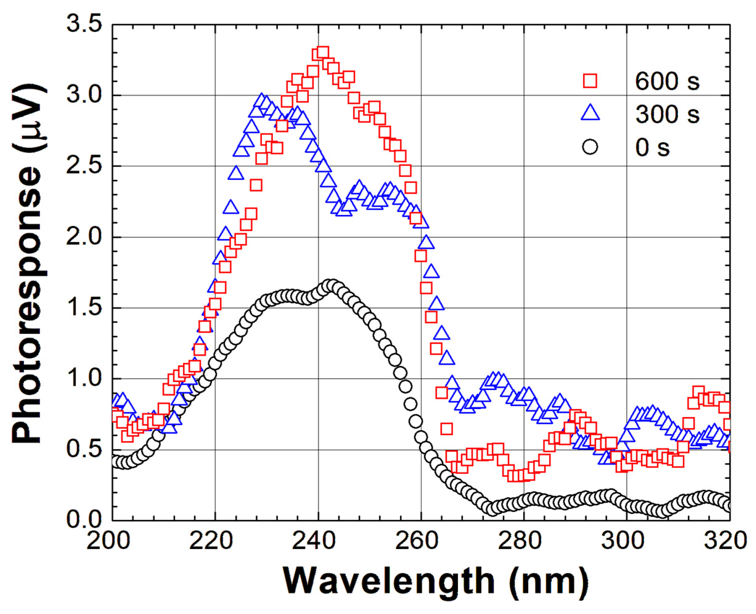
Similar to electron beam injection in Figure 14 and Figure 17, the forward bias charge injection results in an increase of minority carrier diffusion length in 10-μm thick Gallium Oxide layer. Although L was not directly measured, more than 200% increase of the pick photoresponse, shown in Figure 20, provides experimental evidence for its elongation. Ref. [32] reported a similar photoresponse enhancement in forward-biased GaN p-n junction and suggested the mechanism for this effect. Experiments are under way for detailed study of the effect of charge injection in Gallium Oxide device structures, and this will be the subject of future publications.
4. Summary
In summary, while irradiation with energetic particles and increasing temperature lead to decrease of minority carrier diffusion length, charge injection using SEM mitigates the negative influence of radiation on carrier recombination in Ga2O3. It is demonstrated that L, decreased because of energetic particle bombardment, could be returned to the initial values or increase above them. The effect was attributed to non-equilibrium carrier trapping on native defects (VGa) and consequent increase in τ. With Ga2O3 p–n junctions becoming feasible, a solid-state charge injection, due to bias, will be employed (as in Figure 20), thus paving the road towards purely electrical (athermal) mitigation of radiation-induced defects in bipolar devices.
Author Contributions
Conceptualization, L.C..; methodology, S.M., A.S.; software, A.S.; validation, A.S., S.M.; formal analysis, S.M.; investigation, S.M.; writing—original draft preparation, L.C.; writing—review and editing, L.C., A.R.; supervision, L.C.; project administration, L.C.; funding acquisition, L.C. All authors have read and agreed to the published version of the manuscript.
Funding
This research was supported in part by the US-Israel Binational Science Foundation (awards ## 2022056 and 2022779), the National Science Foundation (ECCS #2310285), and NATO (G5748).
Data Availability Statement
The data presented in this review are openly available from the articles cited in this review paper as well as from the corresponding author upon request.
Conflicts of Interest
The authors declare no conflict of interest.
References
- Pearton, S.J.; Yang, J.; Cary, P.H.; Ren, F.; Kim, J.; Tadjer, M.J.; Mastro, M.A. A review of Ga2O3 materials, processing, and devices. Appl. Phys. Rev. 2018, 5, 011301. [Google Scholar] [CrossRef]
- Baliga, B.J. Gallium nitride devices for power electronic applications. Semicond. Sci. Technol. 2013, 28, 074011. [Google Scholar] [CrossRef]
- Chernyak, L.; Osinsky, A.; Schulte, A. Minority carrier transport in GaN and related materials. Solid·State Electron. 2001, 45, 1687–1702. [Google Scholar] [CrossRef]
- Polyakov, A.Y.; Smirnov, N.B.; Shchemerov, I.V.; Pearton, S.J.; Ren, F.; Chernykh, A.V.; Kochkova, A.I. Electrical properties of bulk semi-insulating β-Ga2O3 (Fe). Appl. Phys. Lett. 2018, 113, 142102. [Google Scholar] [CrossRef]
- Gao, H.; Muralidharan, S.; Pronin, N.; Karim, M.R.; White, S.M.; Asel, T.; Foster, G.; Krishnamoorthy, S.; Rajan, S.; Cao, L.R.; et al. Optical signatures of deep level defects in Ga2O3. Appl. Phys. Lett. 2018, 112, 242102. [Google Scholar] [CrossRef]
- Yang, J.; Ren, F.; Pearton, S.J.; Yang, G.; Kim, J.; Kuramata, A. 1.5 MeV electron irradiation damage in β-Ga2O3 vertical rectifiers. J. Vac. Sci. Technol. B:Nanotechnol. Microelectron. 2017, 35, 4. [Google Scholar] [CrossRef]
- Mock, A.; Korlacki, R.; Briley, C.; Darakchieva, V.; Monemar, B.; Kumagai, Y.; Goto, K.; Higashiwaki, M.; Schubert, M. Band-to-band transitions, selection rules, effective mass, and excitonic contributions in monoclinic β−Ga2O3. Phys. Rev. B 2017, 96, 14. [Google Scholar] [CrossRef]
- Mastro, M.A.; Kuramata, A.; Calkins, J.; Kim, J.; Ren, F.; Pearton, S.J. Perspective—Opportunities and Future Directions for Ga2O3. ECS J. Solid State Sci. Technol. 2017, 6, P356–P359. [Google Scholar] [CrossRef]
- Stepanov, S.I.; Nikolaev, V.I.; Bougrov, V.E.; Romanov, A.E. Gallium Oxide: Properties and Applications - A Review. Rev. Adv. Mater. Sci. 2016, 44, 63–86. [Google Scholar]
- Chikoidze, E.; Fellous, A.; Perez-Tomas, A.; Sauthier, G.; Tchelidze, T.; Ton-That, C.; Huynh, T.T.; Phillips, M.; Russell, S.; Jennings, M.; et al. P-type β-gallium oxide: A new perspective for power and optoelectronic devices. Mater. Today Phys. 2017, 3, 118–126. [Google Scholar] [CrossRef]
- Chikoidze, E.; Sartel, C.; Mohamed, H.; Madaci, I.; Tchelidze, T.; Modreanu, M.; Vales-Castro, P.; Rubio, C.; Arnold, C.; Sallet, V.; et al. Enhancing the intrinsic p-type conductivity of the ultra-wide bandgap Ga2O3 semiconductor. J. Mater. Chem. C 2019, 7, 10231–10239. [Google Scholar] [CrossRef]
- Kananen, B.E.; Giles, N.C.; Halliburton, L.E.; Foundos, G.K.; Chang, K.B.; Stevens, K.T. Self-trapped holes in β-Ga2O3 crystals. J. Appl. Phys. 2017, 122, 6. [Google Scholar] [CrossRef]
- Varley, J.B.; Janotti, A.; Franchini, C.; Van de Walle, C.G. Role of self-trapping in luminescence and p-type conductivity of wide-band-gap oxides. Phys. Rev. B 2012, 85, 081109. [Google Scholar] [CrossRef]
- Yoshioka, S.; Hayashi, H.; Kuwabara, A.; Oba, F.; Matsunaga, K.; Tanaka, I. Structures and energetics of Ga2O3 polymorphs. J. Phys. Condens. Matter 2007, 19, 11. [Google Scholar] [CrossRef]
- He, H.; Orlando, R.; Blanco, M.A.; Pandey, R.; Amzallag, E.; Baraille, I.; Rérat, M. First-principles study of the structural, electronic, and optical properties of Ga2O3 in its monoclinic and hexagonal phases. Phys. Rev. B 2006, 74, 8. [Google Scholar] [CrossRef]
- He, H.; Blanco, M.A.; Pandey, R. Electronic and thermodynamic properties of β-Ga2O3. Appl. Phys. Lett. 2006, 88, 261904. [Google Scholar] [CrossRef]
- Furthmüller, J.; Bechstedt, F. Quasiparticle bands and spectra ofGa2O3polymorphs. Phys. Rev. B 2016, 93, 115204. [Google Scholar] [CrossRef]
- Chernyak, L.; Schulte, A. Method and System for Performance Improvement of Photodetectors and Solar Cells. 6,674,064, 2004.
- Lopatiuk-Tirpak, O.; Chernyak, L.; Xiu, F.X.; Liu, J.L.; Jang, S.; Ren, F.; Pearton, S.J.; Gartsman, K.; Feldman, Y.; Osinsky, A.; et al. Studies of minority carrier diffusion length increase in p-type ZnO:Sb. J. Appl. Phys. 2006, 100, 086101. [Google Scholar] [CrossRef]
- Chernyak, L.; Osinsky, A.; Nootz, G.; Schulte, A.; Jasinski, J.; Benamara, M.; Liliental-Weber, Z.; Look, D.C.; Molnar, R.J. Electron beam and optical depth profiling of quasibulk GaN. Appl. Phys. Lett. 2000, 77, 2695–2697. [Google Scholar] [CrossRef]
- Chernyak, L.; Nootz, G.; Osinsky, A. Enhancement of minority carrier transport in forward biased GaN p-n junction. Electron. Lett. 2001, 37, 922–923. [Google Scholar] [CrossRef]
- Chernyak, L.; Osinsky, A.; Fuflyigin, V.; Schubert, E.F. Electron beam-induced increase of electron diffusion length in p-type GaN and AlGaN/GaN superlattices. Appl. Phys. Lett. 2000, 77, 875–877. [Google Scholar] [CrossRef]
- Lopatiuk-Tirpak, O.; Chernyak, L.; Wang, Y.L.; Ren, F.; Pearton, S.J.; Gartsman, K.; Feldman, Y. Cathodoluminescence studies of carrier concentration dependence for the electron irradiation effects in p- GaN. Appl. Phys. Lett. 2007, 90, 3. [Google Scholar] [CrossRef]
- Lopatiuk-Tirpak, O.; Chernyak, L.; Mandalapu, L.J.; Yang, Z.; Liu, J.L.; Gartsman, K.; Feldman, Y.; Dashevsky, Z. Influence of electron injection on the photoresponse of ZnO homojunction diodes. Appl. Phys. Lett. 2006, 89, 142114. [Google Scholar] [CrossRef]
- Modak, S.; Chernyak, L.; Khodorov, S.; Lubomirsky, I.; Yang, J.; Ren, F.; Pearton, S.J. Impact of Electron Injection and Temperature on Minority Carrier Transport in Alpha-Irradiated ß-Ga2O3 Schottky Rectifiers. ECS J. Solid State Sci. Technol. 2019, 8, Q3050–Q3053. [Google Scholar] [CrossRef]
- Modak, S.; Lee, J.; Chernyak, L.; Yang, J.; Ren, F.; Pearton, S.J.; Khodorov, S.; Lubomirsky, I. Electron injection-induced effects in Si-doped β-Ga2O3. AIP Adv. 2019, 9, 015127. [Google Scholar] [CrossRef]
- Modak, S.; Schulte, A.; Sartel, C.; Sallet, V.; Dumont, Y.; Chikoidze, E.; Xia, X.; Ren, F.; Pearton, S.J.; Ruzin, A.; et al. Impact of radiation and electron trapping on minority carrier transport in p-Ga2O3. Appl. Phys. Lett. 2022, 120. [Google Scholar] [CrossRef]
- Chernyak, L.; Burdett, W.; Klimov, M.; Osinsky, A. Cathodoluminescence studies of the electron injection-induced effects in GaN. Appl. Phys. Lett. 2003, 82, 3680–3682. [Google Scholar] [CrossRef]
- Lopatiuk, O.; Burdett, W.; Chernyak, L.; Ip, K.P.; Heo, Y.W.; Norton, D.P.; Pearton, S.J.; Hertog, B.; Chow, P.P.; Osinsky, A. Minority carrier transport in p-type Zn0.9Mg0.1O doped with phosphorus. Appl. Phys. Lett. 2005, 86. [Google Scholar] [CrossRef]
- Lopatiuk, O.; Chernyak, L.; Osinsky, A.; Xie, J.Q. Lithium-related states as deep electron traps in ZnO. Appl. Phys. Lett. 2005, 87. [Google Scholar] [CrossRef]
- Lopatiuk-Tirpak, O.; Nootz, G.; Flitsiyan, E.; Chernyak, L.; Mandalapu, L.J.; Yang, Z.; Liu, J.L.; Gartsman, K.; Osinsky, A. Influence of electron injection on the temporal response of ZnO homojunction photodiodes. Appl. Phys. Lett. 2007, 91. [Google Scholar] [CrossRef]
- Chernyak, L.; Schulte, A.; Osinsky, A.; Graff, J.; Schubert, E.F. Influence of electron injection on performance of GaN photodetectors. Appl. Phys. Lett. 2002, 80, 926–928. [Google Scholar] [CrossRef]
- Lee, J.; Flitsiyan, E.; Chernyak, L.; Yang, J.; Ren, F.; Pearton, S.J.; Meyler, B.; Salzman, Y.J. Effect of 1.5 MeV electron irradiation on β-Ga2O3 carrier lifetime and diffusion length. Appl. Phys. Lett. 2018, 112, 5. [Google Scholar] [CrossRef]
- Modak, S.; Chernyak, L.; Schulte, A.; Xian, M.; Ren, F.; Pearton, S.J.; Lubomirsky, I.; Ruzin, A.; Kosolobov, S.S.; Drachev, V.P. Electron beam probing of non-equilibrium carrier dynamics in 18 MeV alpha particle- and 10 MeV proton-irradiated Si-doped β-Ga2O3 Schottky rectifiers. Appl. Phys. Lett. 2021, 118, 202105. [Google Scholar] [CrossRef]
- Modak, S.; Chernyak, L.; Khodorov, S.; Lubomirsky, I.; Ruzin, A.; Xian, M.; Ren, F.; Pearton, S.J. Effect of Electron Injection on Minority Carrier Transport in 10 MeV Proton Irradiated β-Ga2O3 Schottky Rectifiers. ECS J. Solid State Sci. Technol. 2020, 9, 045018. [Google Scholar] [CrossRef]
- Modak, S.; Chernyak, L.; Schulte, A.; Sartel, C.; Sallet, V.; Dumont, Y.; Chikoidze, E.; Xia, X.; Ren, F.; Pearton, S.J.; et al. Variable temperature probing of minority carrier transport and optical properties in p-Ga2O3. APL Mater. 2022, 10, 031106. [Google Scholar] [CrossRef]
- Dimitriadis, C.A. Determination of bulk diffusion length in thin semiconductor layers by SEM-EBIC. J. Phys. D: Appl. Phys. 1981, 14, 2269–2274. [Google Scholar] [CrossRef]
- Chernyak, L.; Osinsky, A.; Temkin, H.; Yang, J.W.; Chen, Q.; Asif Khan, M. Electron beam induced current measurements of minority carrier diffusion length in gallium nitride. Appl. Phys. Lett. 1996, 69, 2531–2533. [Google Scholar] [CrossRef]
- Yakimov, E.B.; Polyakov, A.Y.; Smirnov, N.B.; Shchemerov, I.V.; Yang, J.; Ren, F.; Yang, G.; Kim, J.; Pearton, S.J. Diffusion length of non-equilibrium minority charge carriers in β-Ga2O3 measured by electron beam induced current. J. Appl. Phys. 2018, 123. [Google Scholar] [CrossRef]
- Ma, N.; Tanen, N.; Verma, A.; Guo, Z.; Luo, T.; Xing, H.; Jena, D. Intrinsic electron mobility limits in β-Ga2O3. Appl. Phys. Lett. 2016, 109, 212101. [Google Scholar] [CrossRef]
- Polyakov, A.Y.; Lee, I.-H.; Smirnov, N.B.; Yakimov, E.B.; Shchemerov, I.V.; Chernykh, A.V.; Kochkova, A.I.; Vasilev, A.A.; Ren, F.; Carey, P.H.; et al. Hydrogen plasma treatment of β-Ga2O3: Changes in electrical properties and deep trap spectra. Appl. Phys. Lett. 2019, 115, 032101. [Google Scholar] [CrossRef]
- Polyakov, A.Y.; Smirnov, N.B.; Shchemerov, I.V.; Yakimov, E.B.; Pearton, S.J.; Fares, C.; Yang, J.; Ren, F.; Kim, J.; Lagov, P.B.; et al. Defects responsible for charge carrier removal and correlation with deep level introduction in irradiated β-Ga2O3. Appl. Phys. Lett. 2018, 113, 092102. [Google Scholar] [CrossRef]
- Adnan, M.M.R.; Verma, D.; Xia, Z.; Kalarickal, N.K.; Rajan, S.; Myers, R.C. Spectral Measurement of the Breakdown Limit of β−Ga2O3 and Tunnel Ionization of Self-Trapped Excitons and Holes. Phys. Rev. Appl. 2021, 16, 034011. [Google Scholar] [CrossRef]
- Chi, Z.; Sartel, C.; Zheng, Y.; Modak, S.; Chernyak, L.; Schaefer, C.M.; Padilla, J.; Santiso, J.; Ruzin, A.; Goncalves, A.-M.; et al. Native defect association in beta-Ga2O3 enables room-temperature p-type conductivity. arXiv 2023, arXiv:2306.01115. [Google Scholar]
- Modak, S.; Chernyak, L.; Xian, M.H.; Ren, F.; Pearton, S.J.; Khodorov, S.; Lubomirsky, I.; Ruzin, A.; Dashevsky, Z. Impact of electron injection on carrier transport and recombination in unintentionally doped GaN. J. Appl. Phys. 2020, 128, 085702. [Google Scholar] [CrossRef]
- Leamy, H.J. Charge collection scanning electron microscopy. J. Appl. Phys. 1982, 53, R51–R80. [Google Scholar] [CrossRef]
- Ahn, S.; Lin, Y.-H.; Ren, F.; Oh, S.; Jung, Y.; Yang, G.; Kim, J.; Mastro, M.A.; Hite, J.K.; Eddy, C.R.; et al. Effect of 5 MeV proton irradiation damage on performance of β-Ga2O3 photodetectors. J. Vac. Sci. Technol. B:Nanotechnol. Microelectron. 2016, 34, 5. [Google Scholar] [CrossRef]
- Armstrong, A.M.; Crawford, M.H.; Jayawardena, A.; Ahyi, A.; Dhar, S. Role of self-trapped holes in the photoconductive gain of β-gallium oxide Schottky diodes. J. Appl. Phys. 2016, 119, 103102. [Google Scholar] [CrossRef]
- Yamaoka, S.; Nakayama, M. Evidence for formation of self-trapped excitons in a β-Ga2O3 single crystal. physica status solidi (c) 2016, 13, 93–96. [Google Scholar] [CrossRef]
- Yamaoka, S.; Furukawa, Y.; Nakayama, M. Initial process of photoluminescence dynamics of self-trapped excitons in a β−Ga2O3 single crystal. Phys. Rev. B 2017, 95, 094304. [Google Scholar] [CrossRef]
- Yamaoka, S.; Mikuni, Y.; Nakayama, M. Photoluminescence polarization characteristics of self-trapped excitons in an undoped β-Ga2O3 single crystal. Journal of Physics: Conference Series 2019, 1220, 012030. [Google Scholar] [CrossRef]
- Frodason, Y.K.; Johansen, K.M.; Vines, L.; Varley, J.B. Self-trapped hole and impurity-related broad luminescence in β-Ga2O3. J. Appl. Phys. 2020, 127, 075701. [Google Scholar] [CrossRef]
- Marcinkevičius, S.; Speck, J.S. Ultrafast dynamics of hole self-localization in β-Ga2O3. Appl. Phys. Lett. 2020, 116, 132101. [Google Scholar] [CrossRef]
- Binet, L.; Gourier, D. Origin of the blue luminescence of β-Ga2O3. J. Phys. Chem. Solid 1998, 59, 1241–1248. [Google Scholar] [CrossRef]
- Blasse, G.; Bril, A. Some observations on the luminescence of b-Ga2O3. J. Phys. Chem. Solids 1970, 31, 707–711. [Google Scholar] [CrossRef]
- Oishi, T.; Koga, Y.; Harada, K.; Kasu, M. High-mobility β-Ga2O3($\bar{2}01$) single crystals grown by edge-defined film-fed growth method and their Schottky barrier diodes with Ni contact. Applied Physics Express 2015, 8, 3. [Google Scholar] [CrossRef]
- Irmscher, K.; Galazka, Z.; Pietsch, M.; Uecker, R.; Fornari, R. Electrical properties of β-Ga2O3 single crystals grown by the Czochralski method. J. Appl. Phys. 2011, 110, 7. [Google Scholar] [CrossRef]
- Lee, J.; Flitsiyan, E.; Chernyak, L.; Ahn, S.; Ren, F.; Yuna, L.; Pearton, S.J.; Kim, J.; Meyler, B.; Salzman, J. Optical Signature of the Electron Injection in Ga2O3. ECS J. Solid State Sci. Technol. 2016, 6, Q3049–Q3051. [Google Scholar] [CrossRef]
- Modak, S.; Chernyak, L.; Schulte, A.; Xian, M.; Ren, F.; Pearton, S.J.; Ruzin, A.; Kosolobov, S.S.; Drachev, V.P. Temperature dependence of cathodoluminescence emission in irradiated Si-doped β-Ga2O3. AIP Adv. 2021, 11, 125014. [Google Scholar] [CrossRef]
- Yu, P.; Cardona, M. Fundamentals of Semiconductors; Springer Berlin Heidelberg: 2010. [CrossRef]
- Yang, J.; Ren, F.; Khanna, R.; Bevlin, K.; Geerpuram, D.; Tung, L.-C.; Lin, J.; Jiang, H.; Lee, J.; Flitsiyan, E.; et al. Annealing of dry etch damage in metallized and bare (-201) Ga2O3. J. Vac. Sci. Technol. B:Nanotechnol. Microelectron. 2017, 35, 5. [Google Scholar] [CrossRef]
- Yang, J.; Fares, C.; Guan, Y.; Ren, F.; Pearton, S.J.; Bae, J.; Kim, J.; Kuramata, A. Eighteen mega-electron-volt alpha-particle damage in homoepitaxial β-Ga2O3 Schottky rectifiers. J. Vac. Sci. Technol. B 2018, 36, 031205. [Google Scholar] [CrossRef]
- Yang, J.; Chen, Z.; Ren, F.; Pearton, S.J.; Yang, G.; Kim, J.; Lee, J.; Flitsiyan, E.; Chernyak, L.; Kuramata, A. 10 MeV proton damage in β-Ga2O3 Schottky rectifiers. J. Vac. Sci. Technol. B:Nanotechnol. Microelectron. 2018, 36. [Google Scholar] [CrossRef]
- Eckstein, M.; Habermeier, H.U. Numerical Analysis of the Temperature Dependence of Ebic and Cl Contrasts. Le Journal de Physique IV 1991, 1, C6. [Google Scholar] [CrossRef]
- Modak, S.; Chernyak, L.; Lubomirsky, I.; Khodorov, S. Continuous and Time-Resolved Cathodoluminescence Studies of Electron Injection Induced Effects in Gallium Nitride. Proceedings of Advanced Technologies for Security Applications, Dordrecht; 2020. [Google Scholar]
- Lin, Y.; Flitsyian, E.; Chernyak, L.; Malinauskas, T.; Aleksiejunas, R.; Jarasiunas, K.; Lim, W.; Pearton, S.J.; Gartsman, K. Optical and electron beam studies of carrier transport in quasibulk GaN. Appl. Phys. Lett. 2009, 95, 092101. [Google Scholar] [CrossRef]
- Godlewski, M.; Lusakowska, E.; Goldys, E.M.; Phillips, M.R.; Bottcher, T.; Figge, S.; Hommel, D.; Prystawko, P.; Leszcynski, M.; Grzegory, I.; et al. Diffusion length of carriers and excitons in GaN-influence of epilayer microstructure. Appl. Surf. Sci 2004, 223, 294–302. [Google Scholar] [CrossRef]
- Cojocaru, L.N. Defect-annealing in neutron-damaged β-Ga2O3. Radiat. EIT. 2006, 21, 157–160. [Google Scholar] [CrossRef]
- Polyakov, A.Y.; Smirnov, N.B.; Shchemerov, I.V.; Yakimov, E.B.; Yang, J.; Ren, F.; Yang, G.; Kim, J.; Kuramata, A.; Pearton, S.J. Point defect induced degradation of electrical properties of Ga2O3 by 10 MeV proton damage. Appl. Phys. Lett. 2018, 112, 032107. [Google Scholar] [CrossRef]
- Kim, J.; Pearton, S.J.; Fares, C.; Yang, J.; Ren, F.; Kim, S.; Polyakov, A.Y. Radiation damage effects in Ga2O3 materials and devices. J. Mater. Chem. C 2019, 7, 10–24. [Google Scholar] [CrossRef]
- Pearton, S.J.; Aitkaliyeva, A.; Xian, M.; Ren, F.; Khachatrian, A.; Ildefonso, A.; Islam, Z.; Jafar Rasel, M.A.; Haque, A.; Polyakov, A.Y.; et al. Review—Radiation Damage in Wide and Ultra-Wide Bandgap Semiconductors. ECS J. Solid State Sci. Technol. 2021, 10, 055008. [Google Scholar] [CrossRef]
- Yakimov, E.B.; Polyakov, A.Y.; Shchemerov, I.V.; Smirnov, N.B.; Vasilev, A.A.; Vergeles, P.S.; Yakimov, E.E.; Chernykh, A.V.; Ren, F.; Pearton, S.J. Experimental estimation of electron–hole pair creation energy in β-Ga2O3. Appl. Phys. Lett. 2021, 118, 202106. [Google Scholar] [CrossRef]
- Karjalainen, A.; Weiser, P.M.; Makkonen, I.; Reinertsen, V.M.; Vines, L.; Tuomisto, F. Interplay of vacancies, hydrogen, and electrical compensation in irradiated and annealed n-type β-Ga2O3. J. Appl. Phys. 2021, 129, 165702. [Google Scholar] [CrossRef]
- Ledra, M.; Tabet, N. Monte Carlo simulation of the EBIC collection efficiency of a Schottky nanocontact. Superlattices and Microstructures 2009, 45, 444–450. [Google Scholar] [CrossRef]
- Yakimov, E.B.; Borisov, S.S.; Zaitsev, S.I. EBIC measurements of small diffusion length in semiconductor structures. Semiconductors 2007, 41, 411–413. [Google Scholar] [CrossRef]
- Donolato, C. Modeling the Ebic Measurements of Diffusion Lengths and the Recombination Contrast at Extended Defects. J. phys., Colloq. 1989, 50, C6. [Google Scholar] [CrossRef]
Figure 1.
Schematics for EBIC measurements. Reprinted with permission from the AIP. After ref. [36].
Figure 1.
Schematics for EBIC measurements. Reprinted with permission from the AIP. After ref. [36].
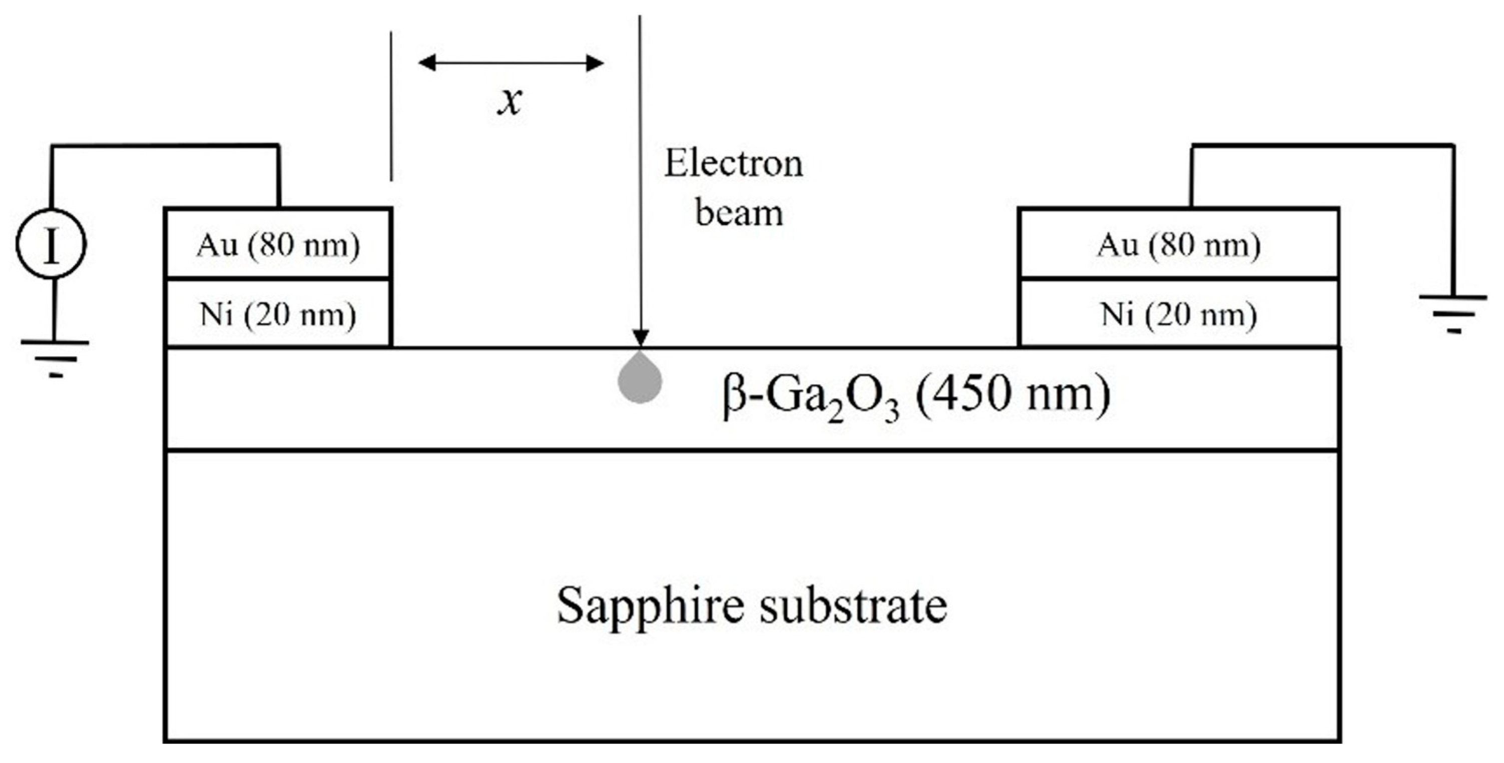
Figure 2.
Raw data for the structure A (a) and the structure B (b) at RT and the fit for extraction of the diffusion length. Reprinted with permission from the AIP. After ref. [36].
Figure 2.
Raw data for the structure A (a) and the structure B (b) at RT and the fit for extraction of the diffusion length. Reprinted with permission from the AIP. After ref. [36].
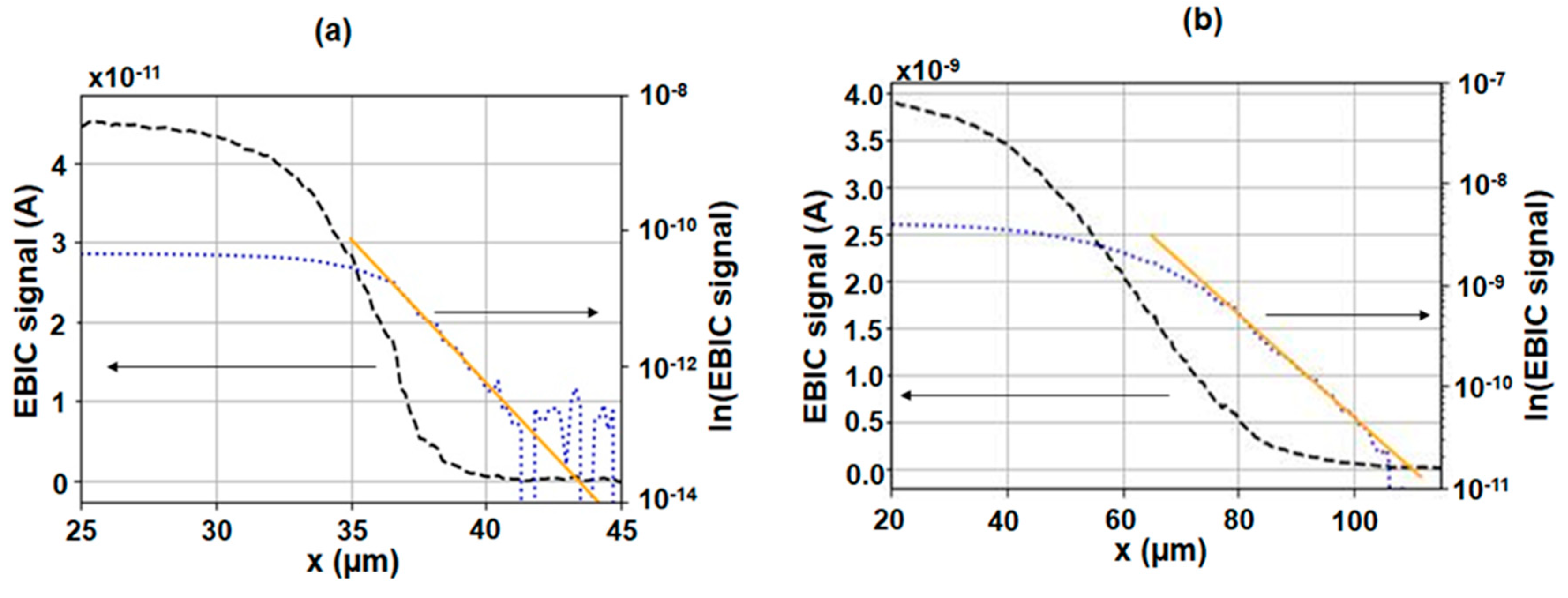
Figure 3.
Diffusion length dependence on temperature for highly resistive p-type samples.
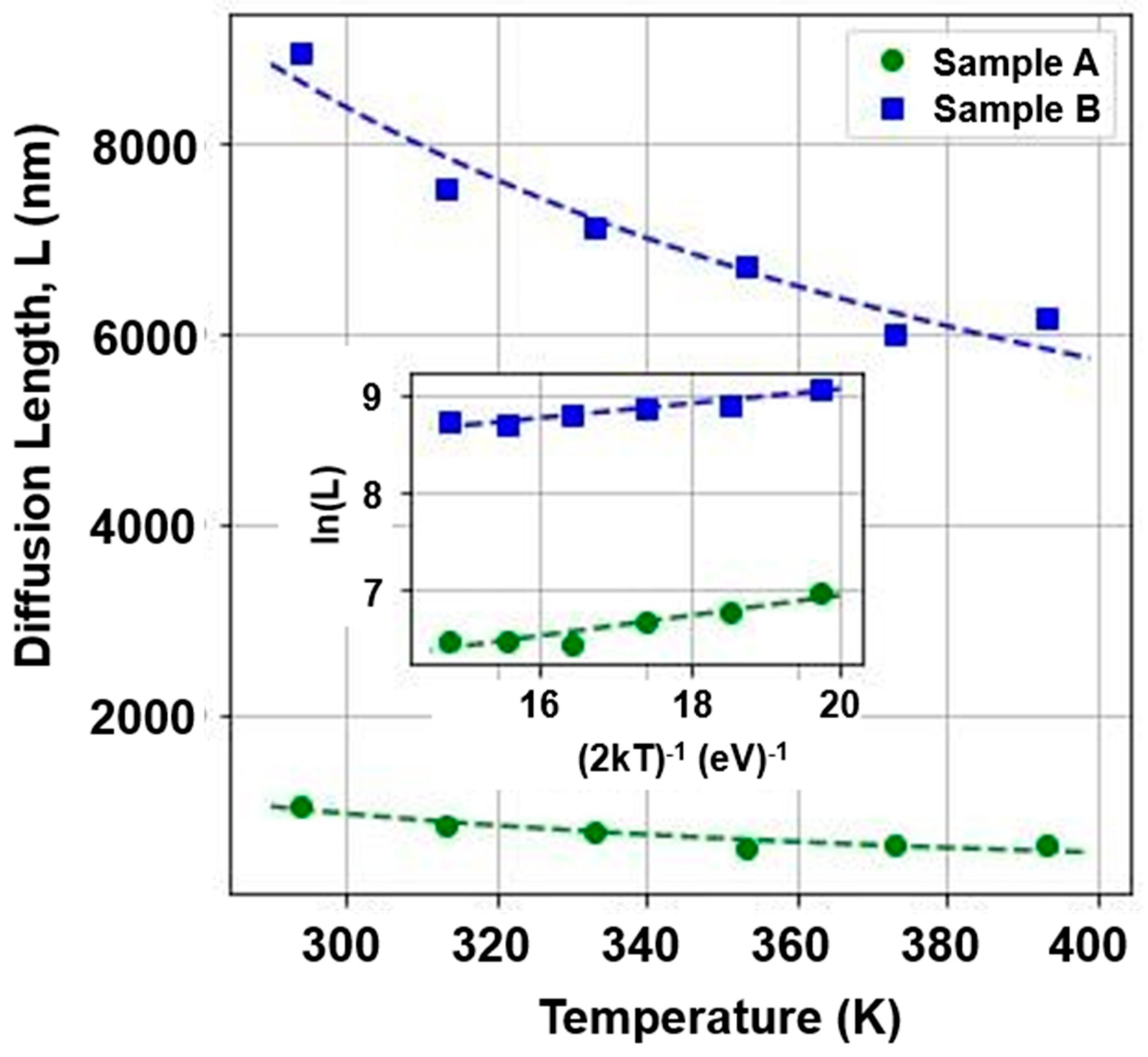
Figure 4.
Left: Time-resolved CL image from a streak camera with a center wavelength of 380 nm. The dashed rectangle shows the region for time decay determination. Right: Normalized spectrum of CL decay at 380 nm with an exponential fit for n-type β-Ga2O3. Lifetime is obtained from the exponential fit inverse slope for the temporal CL decay. Reprinted with permission from the AIP. After ref. [33].
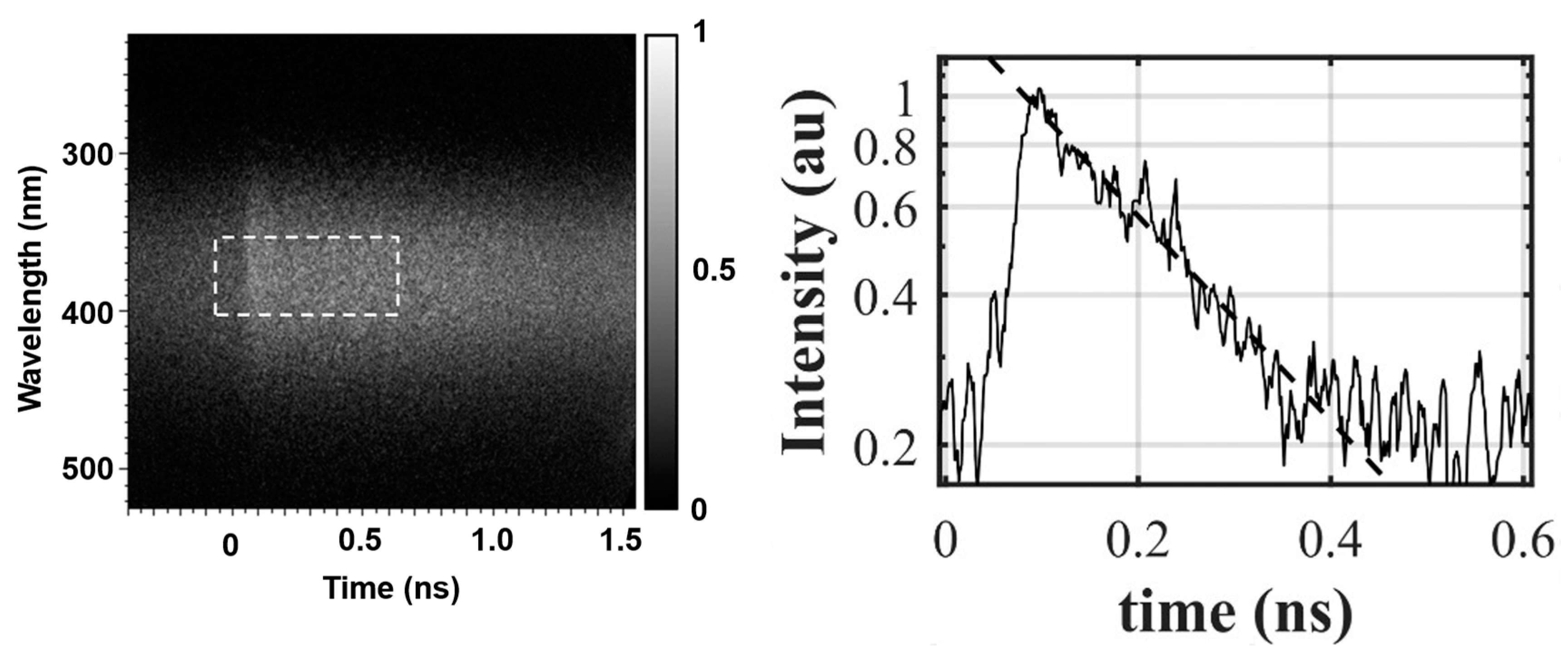
Figure 5.
Experimental setup of Attolight Allallin 4027 Chronos SEM-CL tool capable of sustaining temperatures from 4 K to 310 K.
Figure 5.
Experimental setup of Attolight Allallin 4027 Chronos SEM-CL tool capable of sustaining temperatures from 4 K to 310 K.

Figure 6.
Vertical Schottky rectifiers used for EBIC measurements.
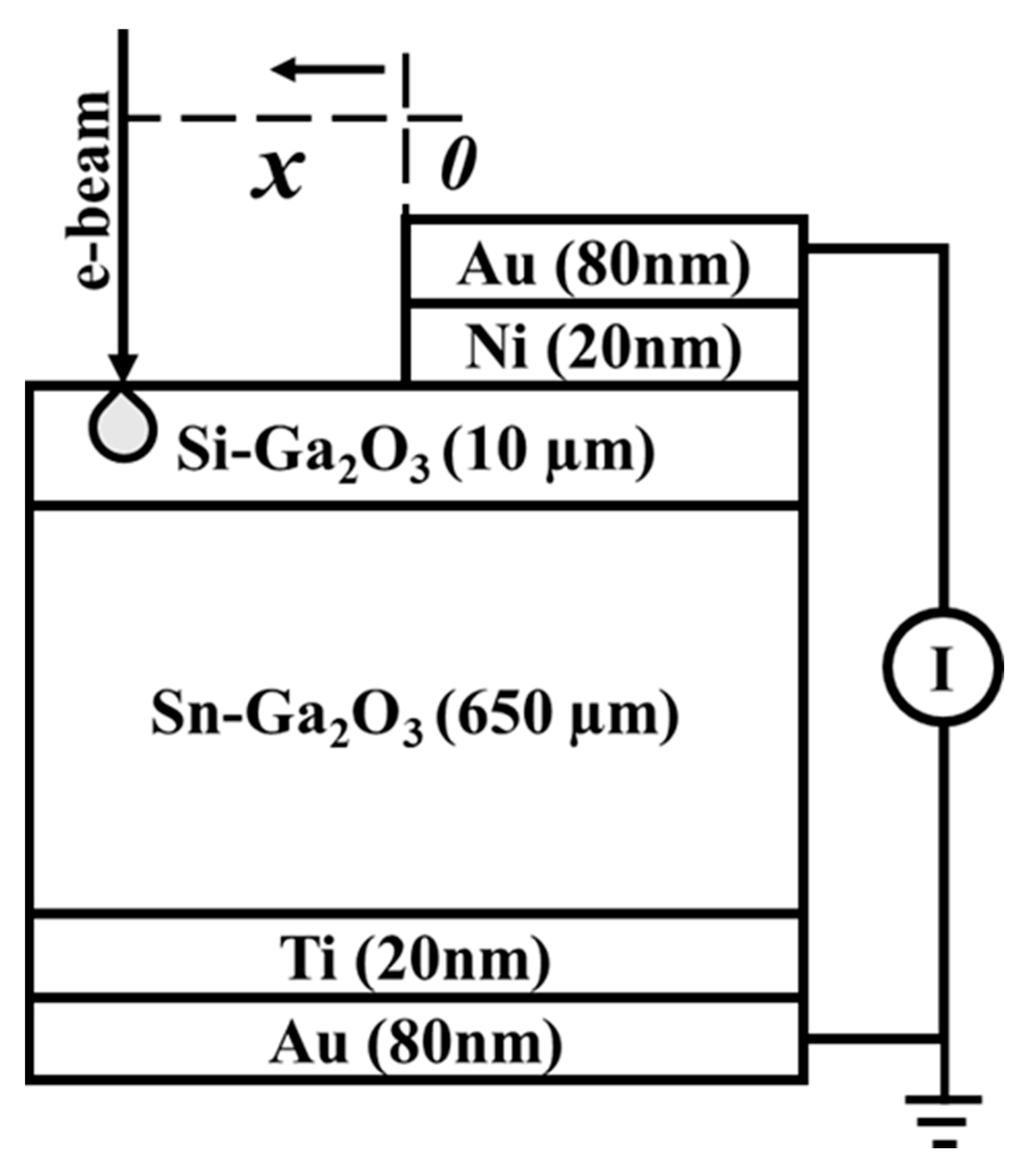
Figure 7.
Dependence of L on T for irradiated and reference samples with fits, revealing activation energy, ΔEL,T. Reprinted with permission from the AIP. After ref. [32,33].
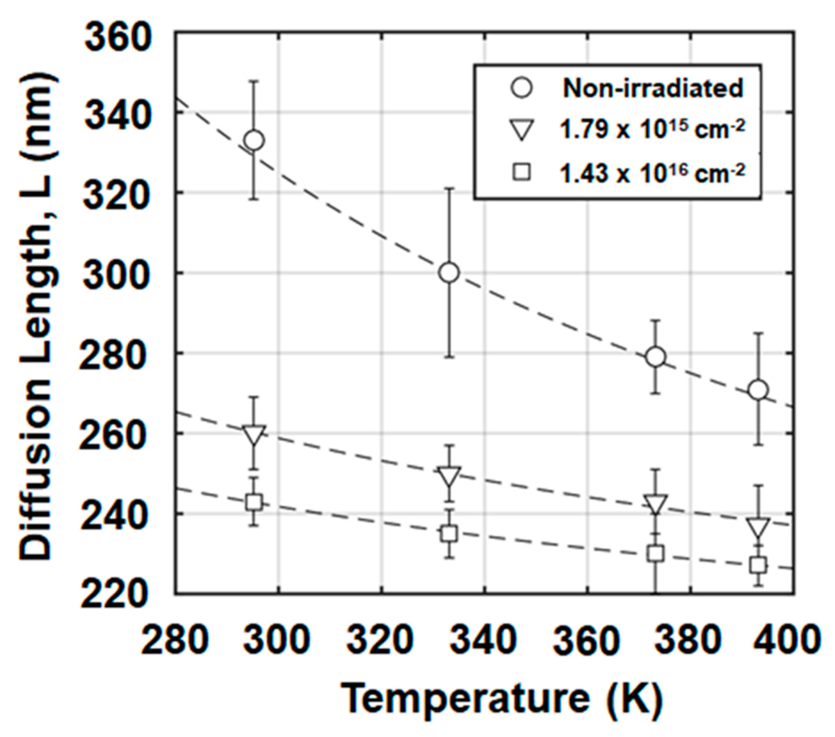
Figure 8.
RT cathodoluminescence spectrum with a Gaussian decomposition, exhibiting bands at 3.65, 3.25, and 2.95 eV and no band-to-band emission (inset). Reprinted with permission from the AIP. After ref. [32,33].
Figure 8.
RT cathodoluminescence spectrum with a Gaussian decomposition, exhibiting bands at 3.65, 3.25, and 2.95 eV and no band-to-band emission (inset). Reprinted with permission from the AIP. After ref. [32,33].
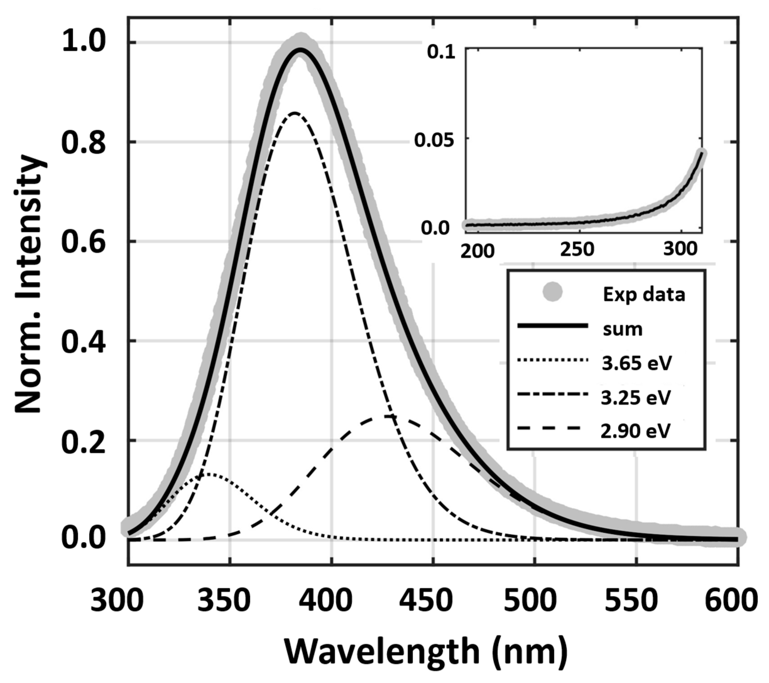
Figure 9.
CL lifetime constant (open circles) for non-irradiated and irradiated samples. The inset shows a CL transient for a non-irradiated sample and an exponential fit (dotted line). Reprinted with permission from the AIP. After ref. [32,33].
Figure 9.
CL lifetime constant (open circles) for non-irradiated and irradiated samples. The inset shows a CL transient for a non-irradiated sample and an exponential fit (dotted line). Reprinted with permission from the AIP. After ref. [32,33].
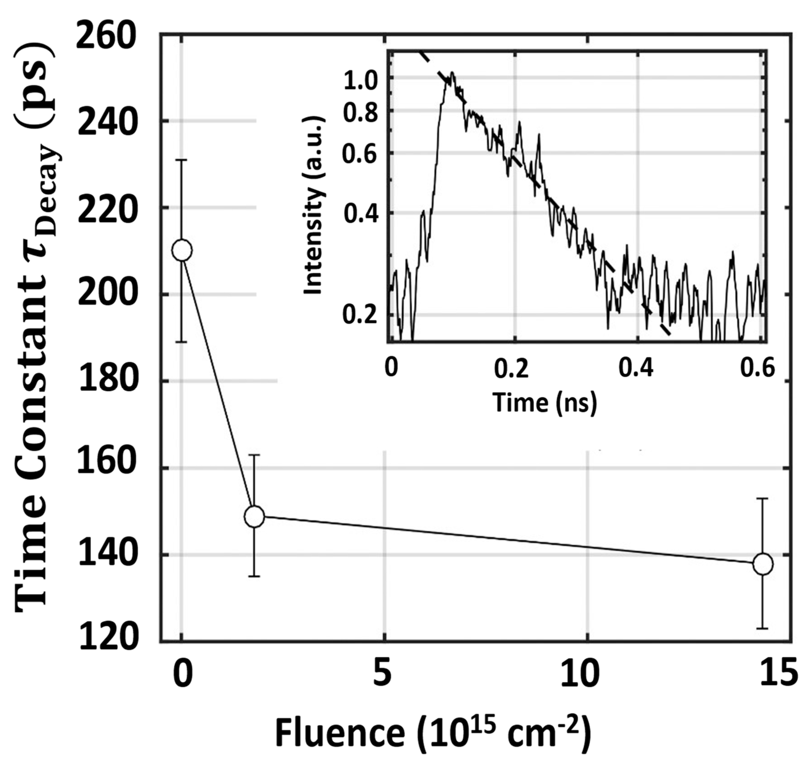
Figure 10.
Temperature dependence of L for various radiation types. Reprinted with permission from the AIP. After ref. [34].
Figure 10.
Temperature dependence of L for various radiation types. Reprinted with permission from the AIP. After ref. [34].
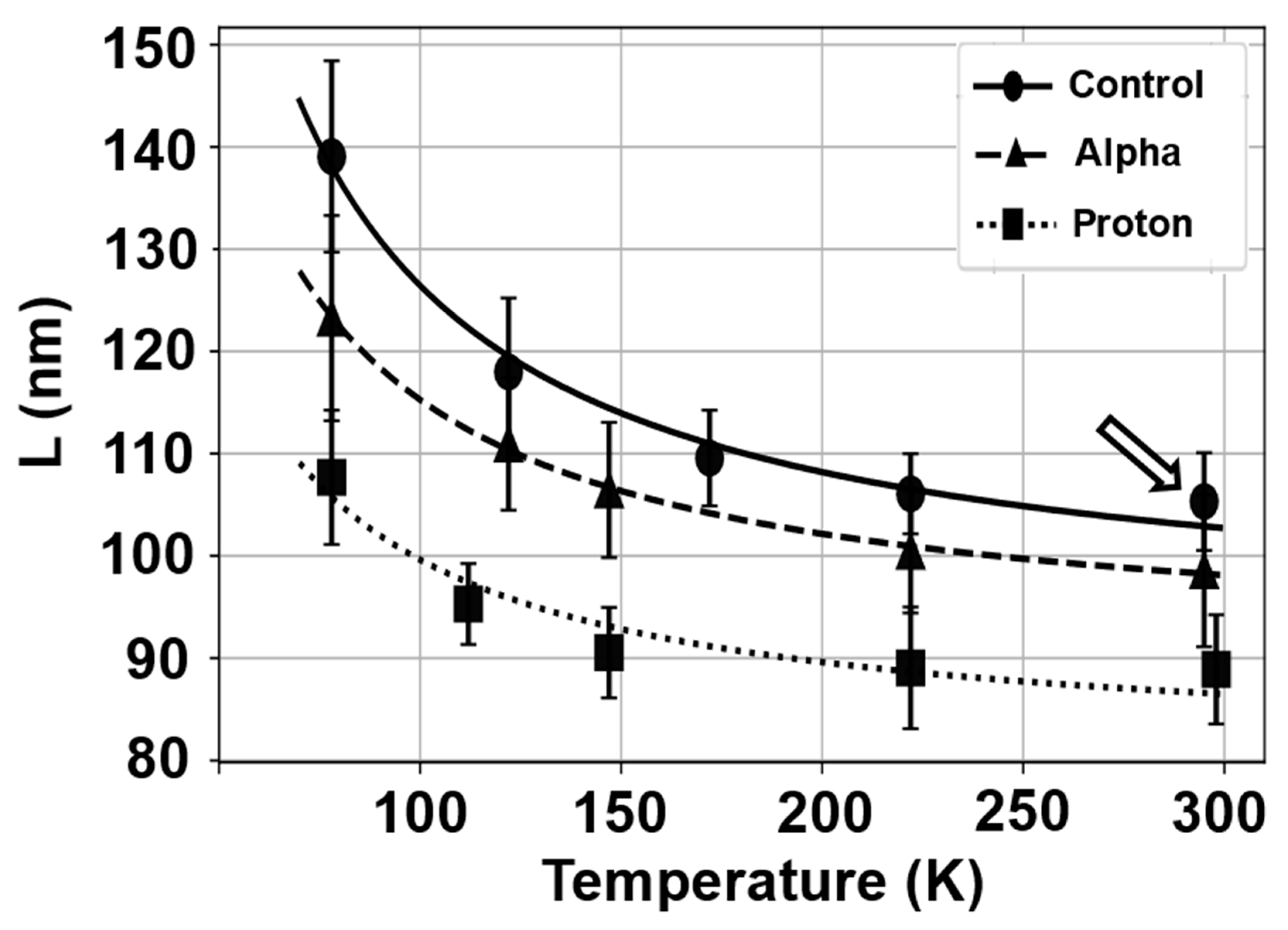
Figure 11.
A streak of time-resolved CL, acquired at RT for reference structure, and its raw image (inset). Reprinted with permission from the AIP. After ref. [34].
Figure 11.
A streak of time-resolved CL, acquired at RT for reference structure, and its raw image (inset). Reprinted with permission from the AIP. After ref. [34].
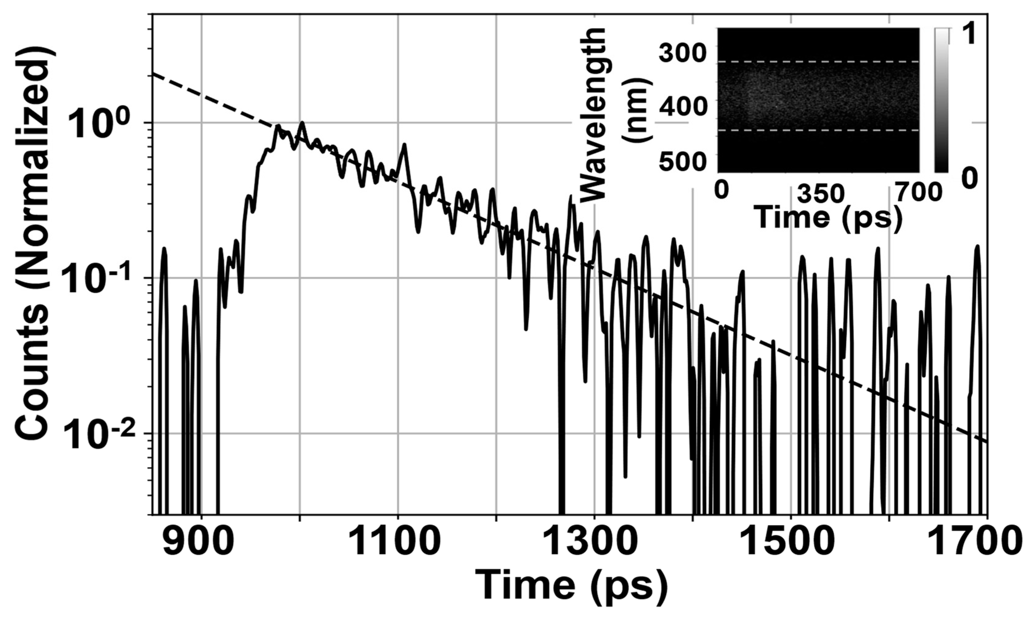
Figure 12.
Lifetime versus temperature dependence for structures irradiated by various particles. Reprinted with permission from the AIP. After ref. [34].
Figure 12.
Lifetime versus temperature dependence for structures irradiated by various particles. Reprinted with permission from the AIP. After ref. [34].
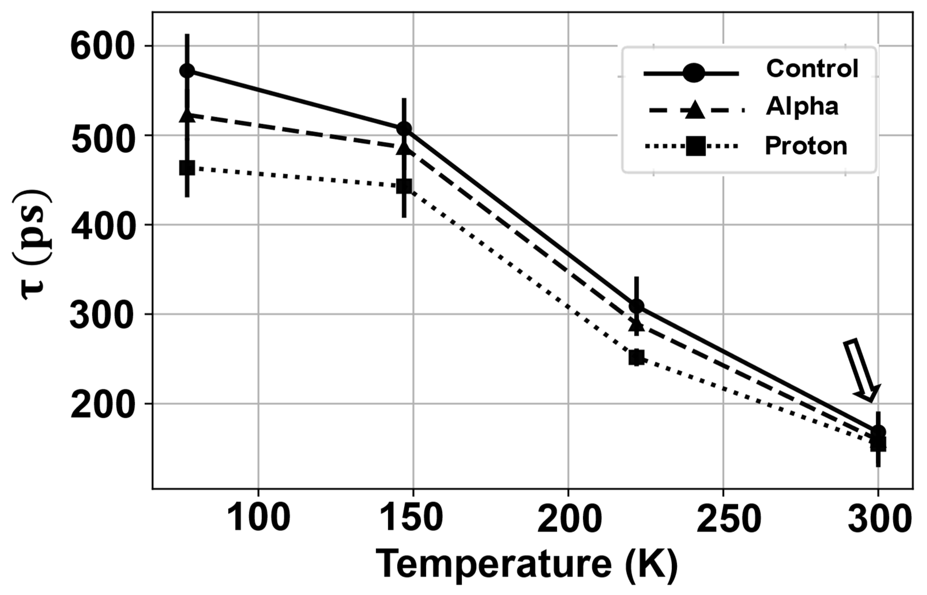
Figure 13.
L versus T dependence prior to and following bombardment with high energy protons having energy/dose sequence as: 25 keV, 1.6 x 1014 cm−2 + 50 keV, 1.7 x 1014 cm−2 + 70 keV, 3.6 x 1014 cm−2. Reprinted with permission from the AIP. After refs. [27,36].
Figure 13.
L versus T dependence prior to and following bombardment with high energy protons having energy/dose sequence as: 25 keV, 1.6 x 1014 cm−2 + 50 keV, 1.7 x 1014 cm−2 + 70 keV, 3.6 x 1014 cm−2. Reprinted with permission from the AIP. After refs. [27,36].
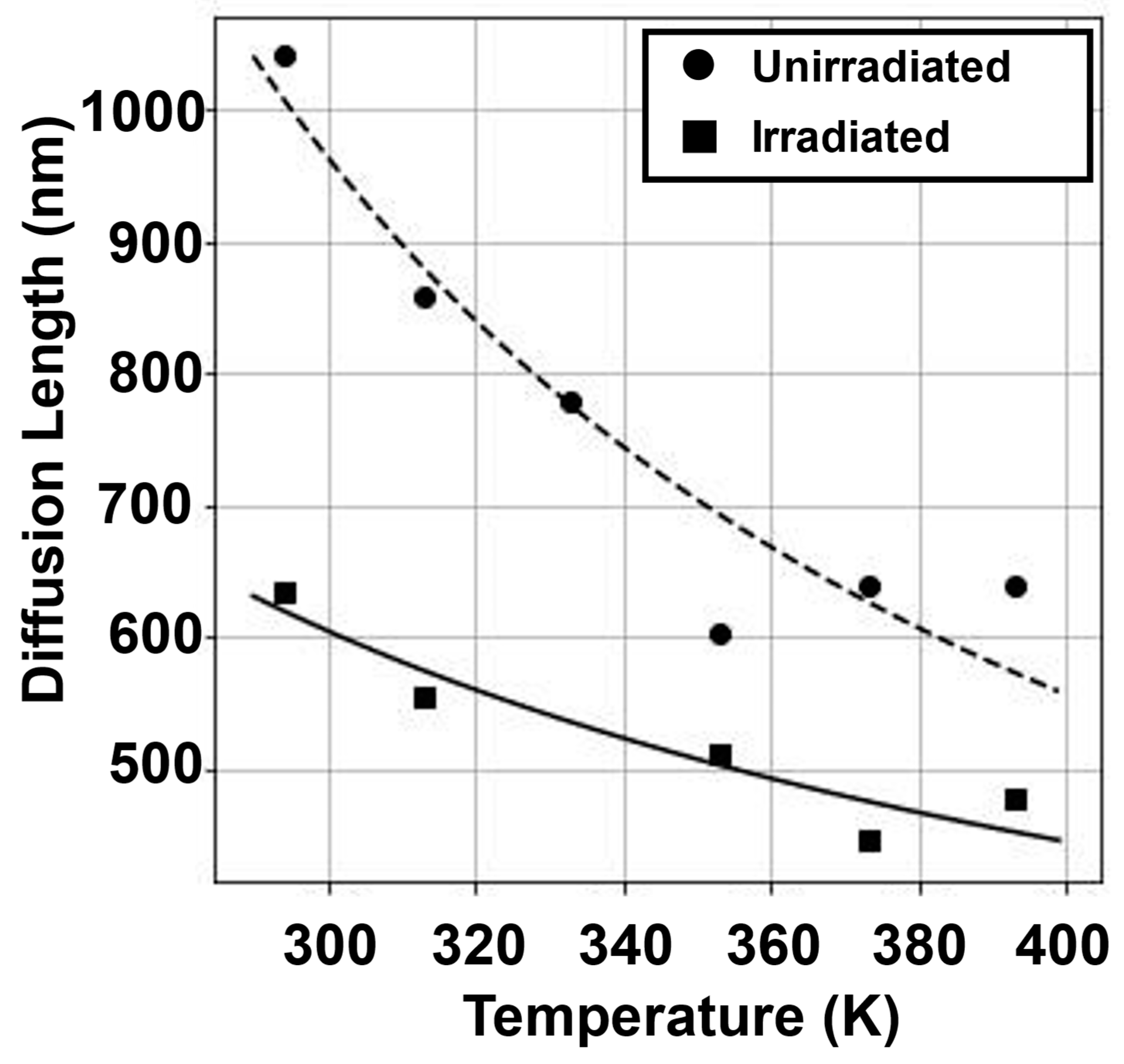
Figure 14.
L versus duration of electron injection dependence at variable temperature for highly resistive p-Ga2O3. L values for 0 injected charge are shown in open circle (21 oC), square (75 oC), and triangle (120 oC). ΔEA,I, obtained from L dependence on injection duration at varying T, is estimated at 91 meV using Equation (6). Reprinted with permission from the AIP. After ref. [27].
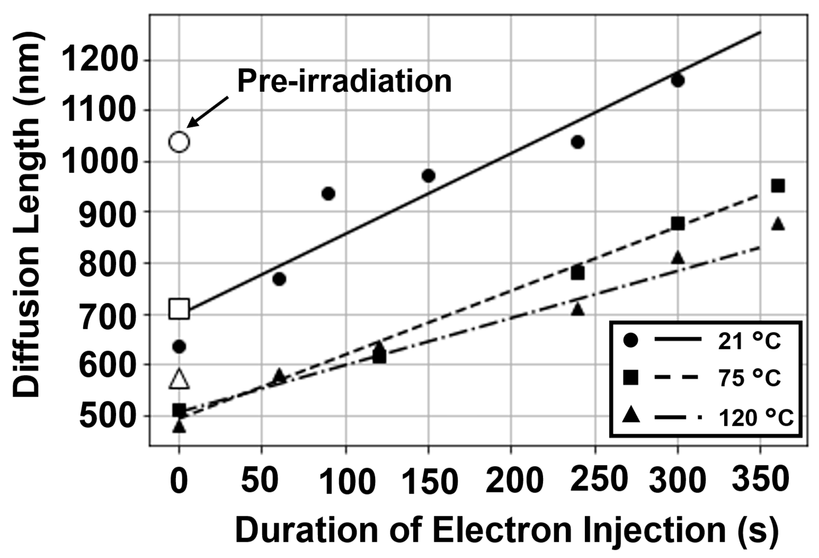
Figure 15.
R versus T dependence. Inset: Arrhenius plot of Equation (6) for calculation of ΔEA,I. Reprinted with permission from the AIP. After ref. [27].
Figure 15.
R versus T dependence. Inset: Arrhenius plot of Equation (6) for calculation of ΔEA,I. Reprinted with permission from the AIP. After ref. [27].
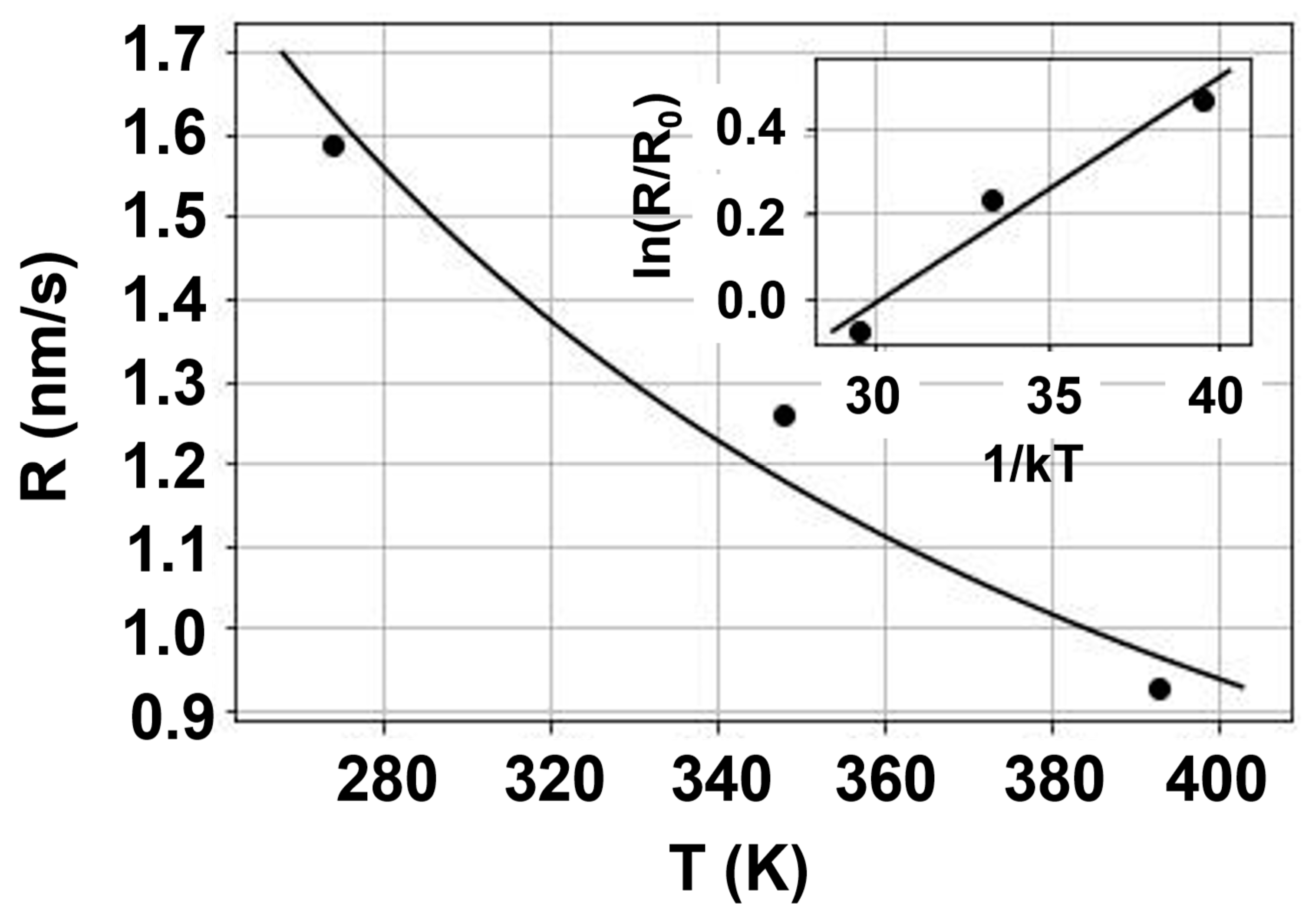
Figure 16.
Normalized continuous RT CL spectrum before and after proton irradiation. A blue shift and smaller full width at half-maximum (FWHM) were observed for CL spectrum after irradiation. Reprinted with permission from the AIP. After ref. [27].
Figure 16.
Normalized continuous RT CL spectrum before and after proton irradiation. A blue shift and smaller full width at half-maximum (FWHM) were observed for CL spectrum after irradiation. Reprinted with permission from the AIP. After ref. [27].
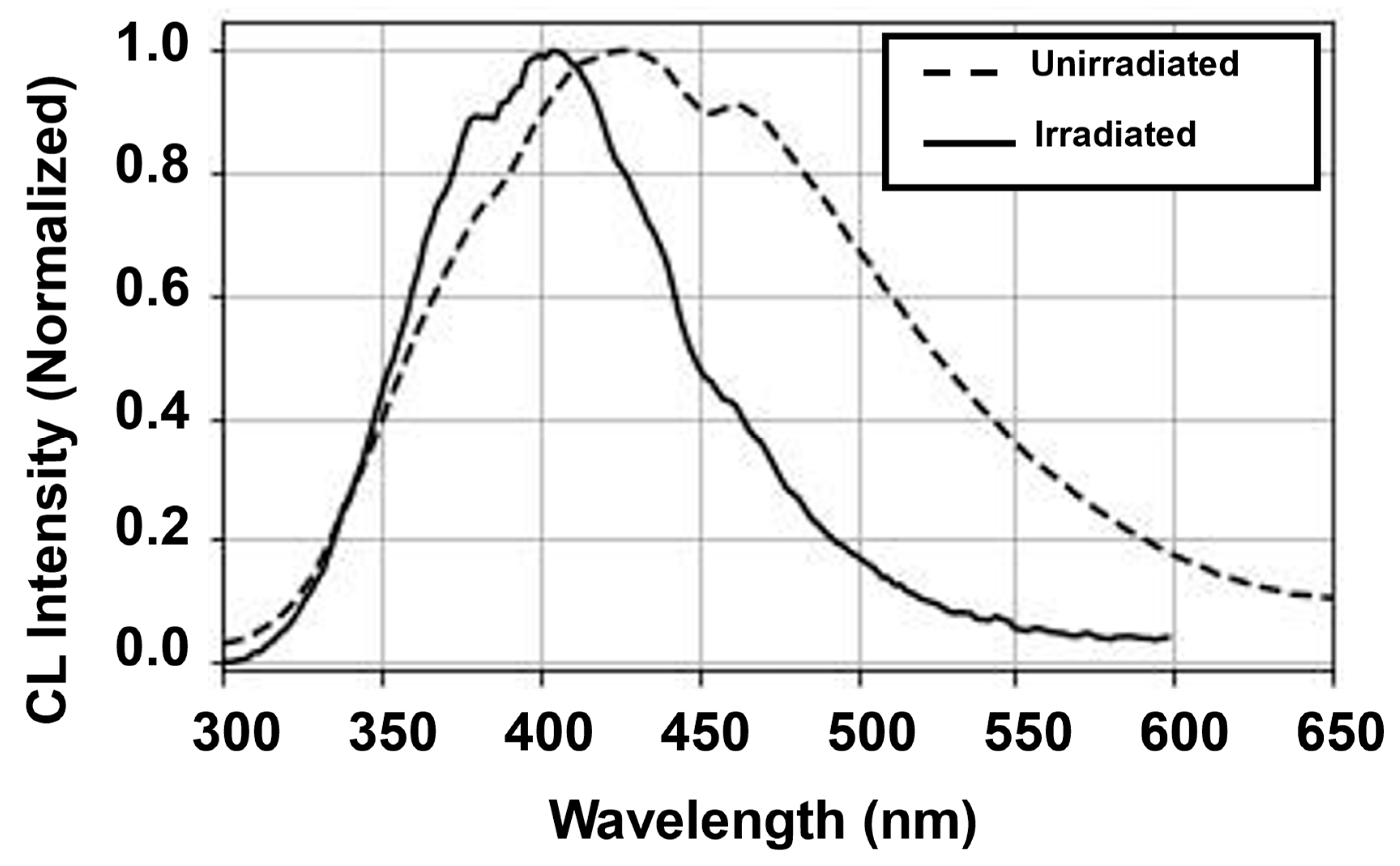
Figure 17.
L increase as a function of electron beam injection. Inset (top): EBIC line-scans for different incremental electron injection durations. Inset (bottom): Electron Beam-Induced Current amplitude dependence on duration of injection. Reprinted with permission from the AIP. After ref. [26].
Figure 17.
L increase as a function of electron beam injection. Inset (top): EBIC line-scans for different incremental electron injection durations. Inset (bottom): Electron Beam-Induced Current amplitude dependence on duration of injection. Reprinted with permission from the AIP. After ref. [26].
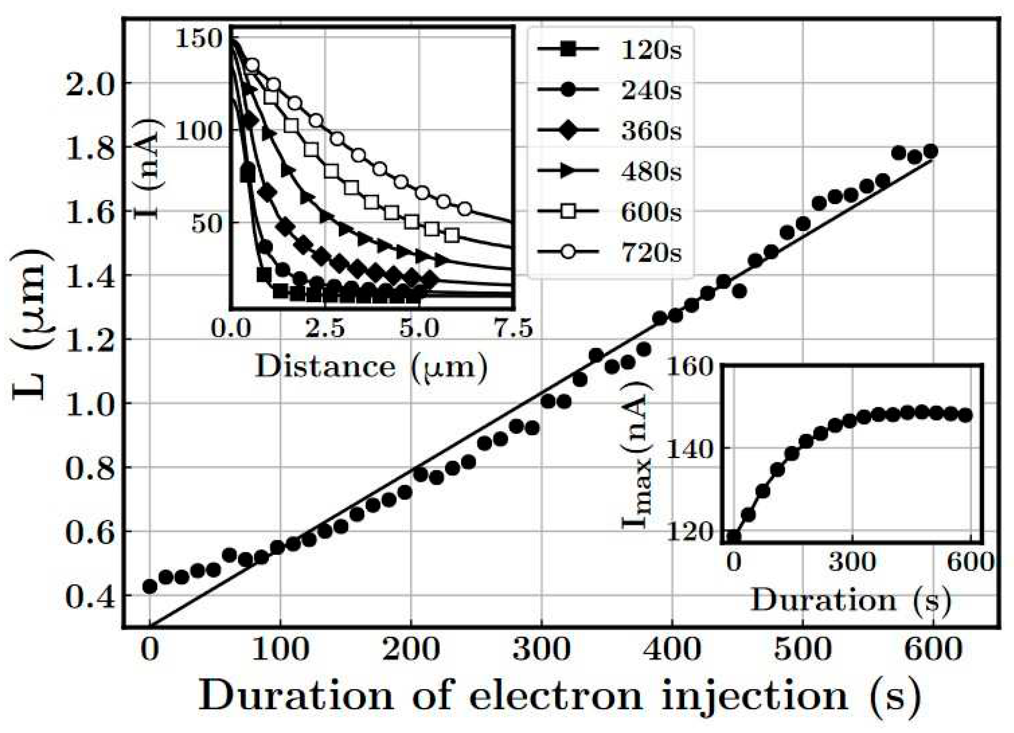
Figure 18.
Model for the electron injection-induced effect (on the example of electron beam irradiation, which generates non-equilibrium electron-hole pairs). Reprinted with permission from the American Institute of Physics. After ref. [45].
Figure 18.
Model for the electron injection-induced effect (on the example of electron beam irradiation, which generates non-equilibrium electron-hole pairs). Reprinted with permission from the American Institute of Physics. After ref. [45].
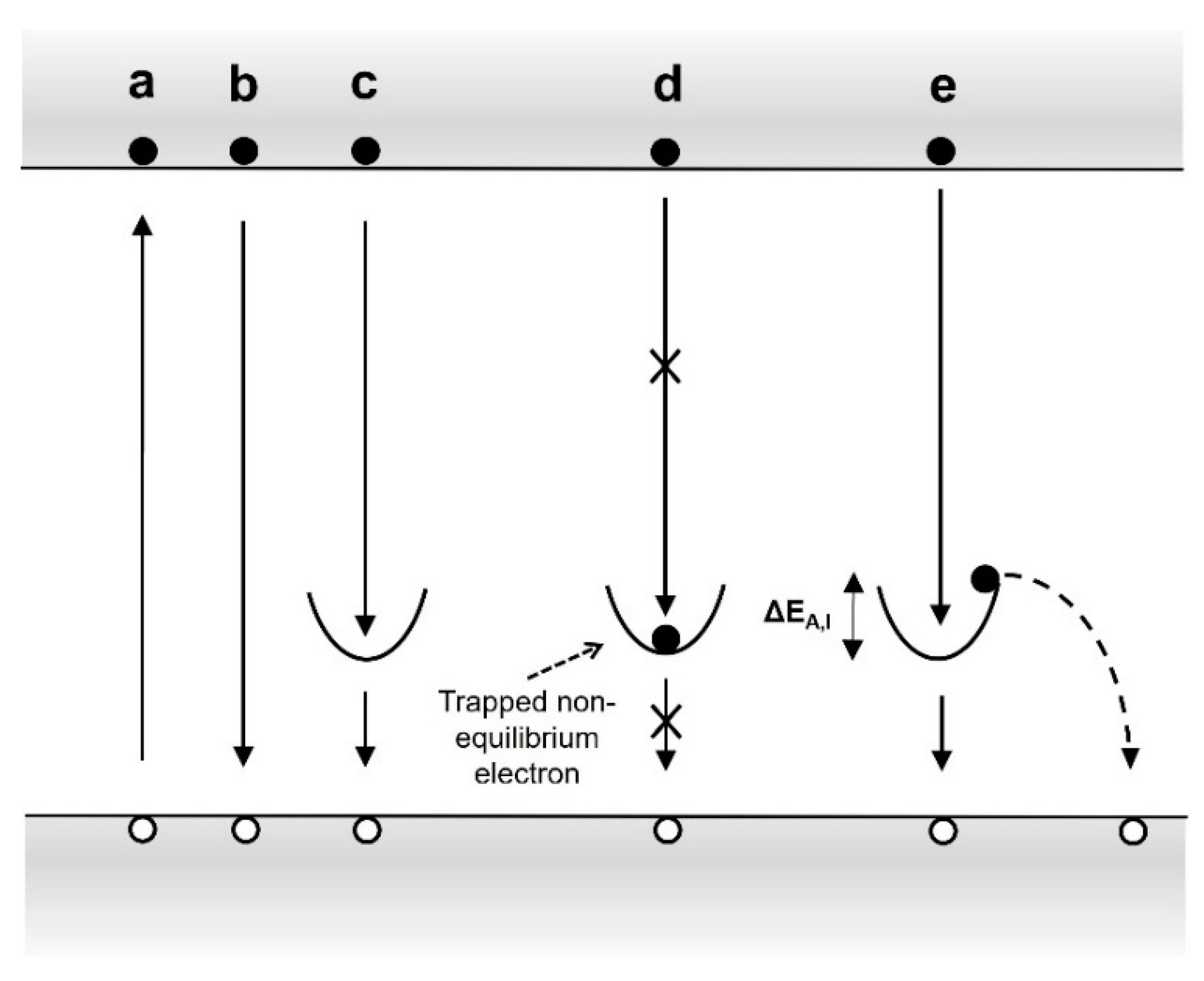
Figure 19.
Architecture of the vertical p-NiO/n-Ga2O3 heterojunction structure (courtesy of Profs. S.J. Pearton and Fan Ren of the University of Florida).
Figure 19.
Architecture of the vertical p-NiO/n-Ga2O3 heterojunction structure (courtesy of Profs. S.J. Pearton and Fan Ren of the University of Florida).
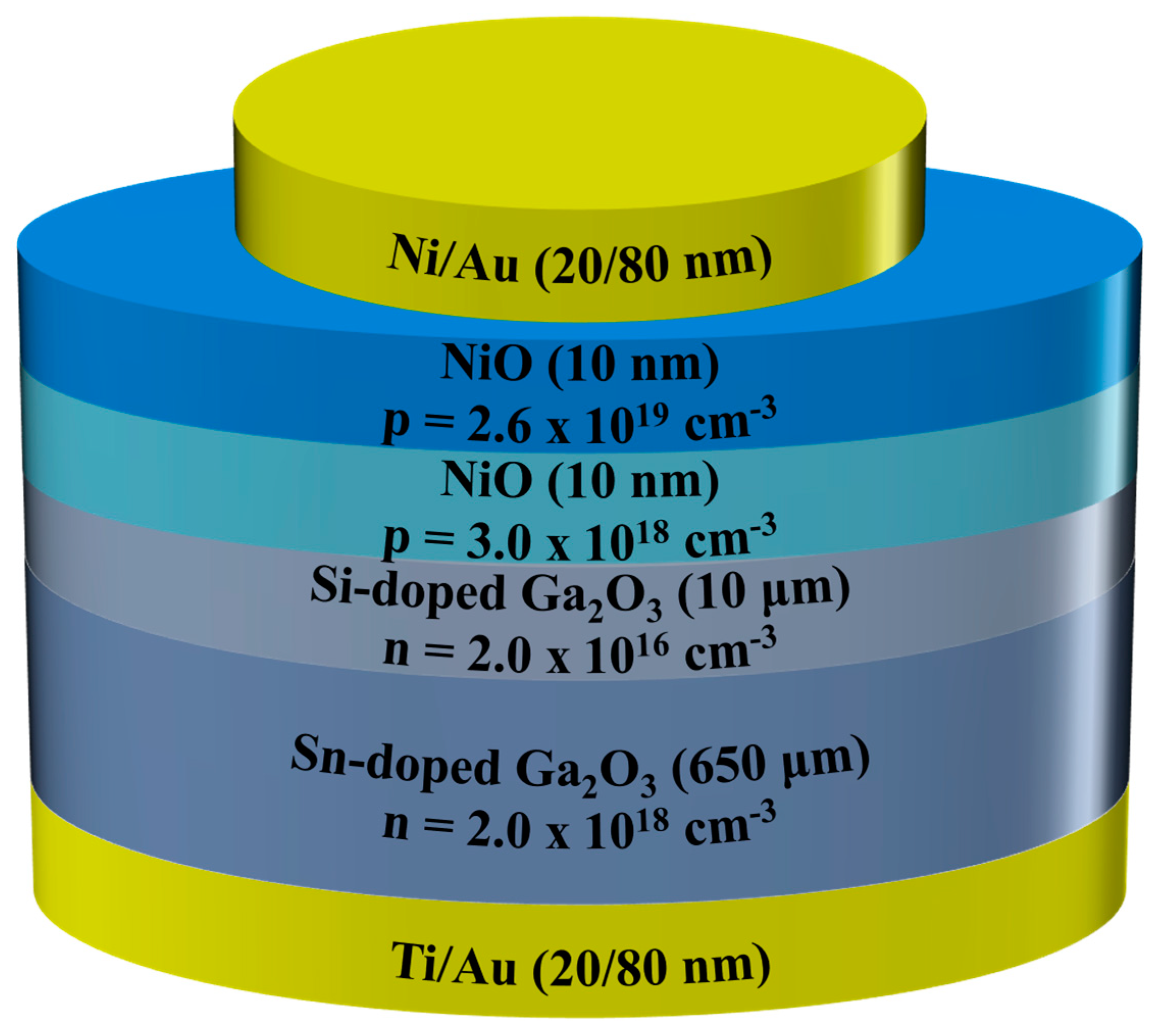
Figure 20.
Spectral photoresponse of the structure in Figure 19 before and after incremental charge injection. The charge, corresponding to 600 seconds of injection, is 60 mC. The effect persists for at least several hours.
Figure 20.
Spectral photoresponse of the structure in Figure 19 before and after incremental charge injection. The charge, corresponding to 600 seconds of injection, is 60 mC. The effect persists for at least several hours.
Disclaimer/Publisher’s Note: The statements, opinions and data contained in all publications are solely those of the individual author(s) and contributor(s) and not of MDPI and/or the editor(s). MDPI and/or the editor(s) disclaim responsibility for any injury to people or property resulting from any ideas, methods, instructions or products referred to in the content. |
© 2023 by the authors. Licensee MDPI, Basel, Switzerland. This article is an open access article distributed under the terms and conditions of the Creative Commons Attribution (CC BY) license (http://creativecommons.org/licenses/by/4.0/).
Copyright: This open access article is published under a Creative Commons CC BY 4.0 license, which permit the free download, distribution, and reuse, provided that the author and preprint are cited in any reuse.


