
Submitted:
28 August 2023
Posted:
30 August 2023
You are already at the latest version
Abstract
GaN nanowires grown on metal substrates attract an increasing interest for a wide range of applications. Herein, we report GaN nanowires grown by plasma-assisted molecular beam epitaxy on thin polycrystalline ZrN buffer layers, sputtered onto Si(111) substrates. The nanowire orientation is studied experimentally and described within a model as a function of the Ga beam angle, nanowire tilt angle and substrate rotation. We show that vertically aligned nanowires grow faster than inclined nanowires, which leads to an interesting effect of geometrical selection of the nanowire orientation in the directional molecular beam epitaxy technique. After a given growth time, this effect depends on the nanowire surface density. At low density, the nanowires continue to grow with random orientations as nucleated. At high density, the effect of preferential growth induced by unidirectional supply of material in MBE starts to dominate. Faster growing nanowires with smaller tilt angles shadow more inclined nanowires that grow slower. This helps to obtain more regular ensembles of vertically oriented GaN nanowires despite their random position induced by the metallic grains at nucleation. The obtained dense ensembles of vertically aligned GaN nanowires on ZrN/Si(111) surfaces are highly relevant for device applications. These results are not specific for GaN nanowires and should be relevant for any nanowires which are epitaxially linked to the randomly oriented surface grains in the directional molecular beam epitaxy.
Keywords:
GaN nanowires
; ZrN buffer layers
; molecular beam epitaxy
; nanowire orientation
; geometrical selection
1. Introduction
III-nitride nanowires (NWs) provide an attractive alternative for planar structures in micro- and optoelectronic devices. Due to a small footprint in contact with a substrate surface, NWs are free of misfit dislocations even when grown on highly lattice-mismatched substrates [1]. As a result, NWs are of superior structural quality which is not achievable in comparable planar heterostructures [2,3,4]. The process of self-assembled growth of GaN NWs by molecular beam epitaxy (MBE) has been thoroughly investigated, especially for amorphous substrates such as nitridated Si [1,4,5,6,7,8,9], SiOx [10,11] and AlxOy [12,13,14]. A specifically attractive benefit offered by the self-assembled growth of GaN NWs on such substrates is that the epitaxial constraints are very weak and the NWs grow perpendicular to the substrate surface [9]. Consequently, ensembles of well-aligned vertical NWs of equal height are formed, which is crucial for the subsequent processing and fabrication of NW-based light emitting devices such as LEDs. Unfortunately, SiO2, AlxOy and SiNx buffer layers form non-ohmic electrical contacts to GaN. This hinders carrier transport and heat dissipation at the NW/substrate interface [15]. Furthermore, due to the optical transparency of SiO2, AlxOy and SiNx buffers, a large part of light generated in the LED quantum well is lost by its absorption in a Si carrier wafer. Thus, various alternative substrates for GaN NW-based devices are still tested.
There is an increasing interest in growing GaN NWs on metal substrates [16,17,18,19,20,21,22,23,24]. Such substrates exhibit excellent electrical and thermal conductivities as well as a high optical reflectance. However, direct MBE growth of GaN NWs on metallic surfaces is challenging. Calabrese et al. [25] reported efficient reactions of TiN/sapphire substrates with the impinging Ga flux, resulting in the surface roughening at high temperatures. Macroscopic delamination of Mo and Ti films from Si substrate at high temperature was also observed [16]. Since GaN NWs are epitaxially linked to the underlying metal [17,20], spatial orientation of the NWs is determined by the mosaic structure of a metallic surface. For example, May et al. [18] observed GaN NWs uniformly tilted with respect to the surface normal within the individual grains of polycrystalline Ta and Ti foils. Transmission electron microscopy studies of GaN NWs on TiN substrates clearly showed the epitaxial relationships [2−1−10] GaN//[011]TiN and (0002)GaN//(111)TiN [20]. Thus, GaN NWs are usually locally textured with respect to the underlining metallic grains, eventually making them impractical for applications requiring vertical NW ensembles. The growth of GaN NWs on monocrystalline metallic substrates of proper crystallographic orientation solves the problem [24], but makes the whole fabrication procedure much more complicated.
In this paper, we report plasma-assisted MBE (PAMBE) growth of GaN NWs on thin polycrystalline ZrN buffer layers, sputtered onto Si(111) substrates. We study experimentally and describe within a dedicated model the growth rate of GaN NWs as a function of the Ga beam angle, the NW tilt angle (induced by the randomly oriented metallic grains), with and without substrate rotation. It is demonstrated that the MBE system geometry has the direct and dominant influence on the NWs orientation. The axial NW growth rate generally decreases with the NW tilt angle, which is why vertically aligned NWs grow faster than inclined NWs, and become dominant in the ensemble for longer growth times or higher NW surface density. It is shown that uniform ensembles of vertical GaN NWs, as required in device applications, can be obtained on polycrystalline ZrN buffer at high enough NW density despite random orientation of metallic grains on which the epitaxially linked NWs nucleate. Geometry of the MBE overcompensates random orientation of initial GaN crystallites induced by metallic grains. These results, including the effect of geometrical selection of vertically aligned NWs, are not limited to a particular material system, but rather are inherent to the NW growth by the directional MBE technique in general.
2. Materials and Methods
The NW samples were grown by PAMBE in a RIBER Compact 21 system, using an Addon radio frequency nitrogen source and a solid-source effusion Ga cell. Si(111) substrates were covered with a 20 nm thick ZrN buffer layer using DC sputtering from a ZrN target. Layer deposition was performed at room temperature under an Ar pressure of 1×10⁻² mbar and a deposition rate of 0.3 nm/s. The ZrN/Si substrates were transferred in air to the PAMBE system, heated to 150°C for 1h in the loading chamber and subsequently to 500°C for 5h in the preparation chamber to remove any volatile contaminating species before the transfer to the growth chamber. After heating the substrate to a required temperature, the PAMBE growth process was initiated by simultaneously opening the Ga and N shutters. GaN NWs were grown under N-rich conditions keeping a N and Ga impinging fluxes of ФN = 16 nm/min and ФGa = 8 nm/min, respectively. Cross-sectional scanning electron microscopy (SEM) of thick GaN(0001) films grown under slightly N- and Ga-rich conditions at low temperatures (680 °C) was used to calibrate the Ga and N fluxes in the 2D-equivalent growth rate units of nm/min [26]. Stability of the N flux was controlled during growth using an optical sensor of plasma light emission attached to the plasma cell [27]. In the standard growth experiments, the substrate was rotated at 6 rpm. However, experiments without substrate rotation were performed as well. The morphology of as-grown GaN NW ensembles was examined using a field-emission Hitachi Su-70 SEM. X-ray diffraction (XRD) measurements of the ZrN/Si substrates as well as of GaN NWs on ZrN buffers were performed using a Panalytical X’Pert Pro-MRD diffractometer equipped with an X-ray lamp with Cu anode, hybrid two-bounce Ge (220) monochromator and Soller slits in front of a Pixcel detector.
3. Results and discussion
3a. Microstructure of ZrN buffer layers on Si(111) substrates
Figure 1 (a) shows the θ/2θ scans of ZrN layer on Si(111) substrate, measured in a wide range of diffracted angles. The XRD signals from Si(111) substrate and from polycrystalline cubic ZrN layer (indicated via JCPDF card no. 00-031-1493) are clearly visible. To eliminate the risk that another lines, originating, for example, from orthorhombic Zr3N4 phase, are overlapped by strong Si peaks, we also measured the same sample by grazing incidence X-ray diffraction (GIXRD) [28] using a beam incident angle of ω = 0.5°. As seen in Figure 1 (b), the diffracted signal from Si(111) substrate was eliminated, while the ZrN lines were identical to those observed under the standard XRD geometry. This proves a single-phase polycrystalline cubic structure of the ZrN film. In order to determine the average grain size of ZrN, we used the size-strain plot procedure [29]. The grain size was estimated by fitting the 111, 200, 220 and 311 diffraction peaks using the Voight function. The Lorentzian component of the full width at half maximum (FWHM) was then used for determining the average crystalline size with different orientation using the Debye-Scherrer formula [30]. Such procedure resulted in the grain size in our ZrN films of about 20 nm. In addition, atomic force microscopy studies (not shown) evidenced very smooth surfaces of the buffer layers with an RMS value of 0.15 nm.
3b. Arrangement of GaN NWs on ZrN/Si substrates
Figure 2(a) shows the SEM image of a typical GaN NW ensemble obtained on polycrystalline ZrN buffer. The NWs have an average diameter of 70 nm and average length of around 1 μm. The NW density determined from plane view SEM images is ~1×1011 cm-2, which is a typical value for self-assembled GaN NWs on nitridated Si substrates [10,11] or AlxOy [31] buffers. The NWs are mostly aligned along the substrate normal. This is a surprising finding, because the initial orientation of the NWs should be directly determined by the formation of epitaxial link between the NWs and the randomly oriented substrate grains. Additionally, small GaN crystallites marked by arrows in Figure 2(b) are clearly seen on the substrate surface between the NWs.
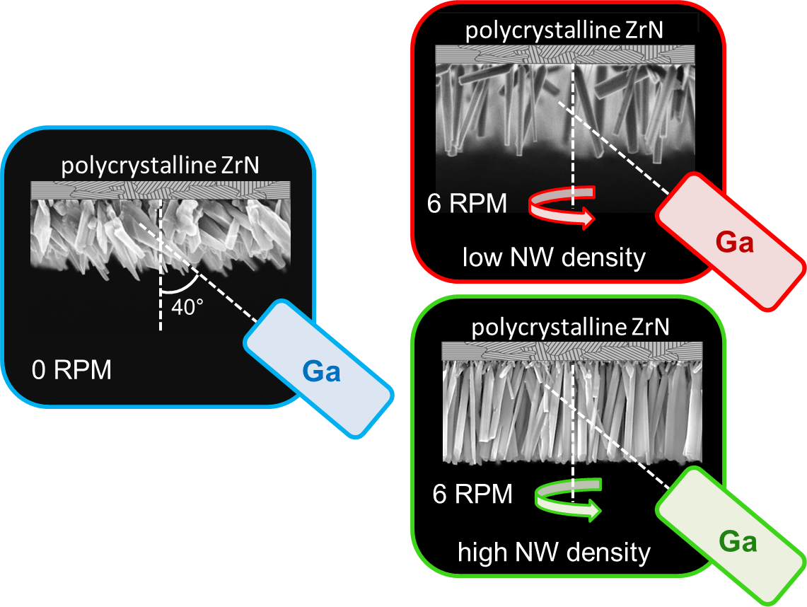
Quite different growth behavior was observed when the NWs were formed under the same growth conditions but without substrate rotation. Figure 3 shows the SEM image of GaN NW ensemble formed in that way. The surface density of these NWs is similar to that obtained with substrate rotation. However, instead of adopting vertical orientation, most NWs grew inclined in a specific direction. The sample was cleaved in the plane defined by the substrate normal and the line-of-sight of the Ga source. During the SEM measurements, the sample position was carefully adjusted to keep the sample cross-section parallel to the imaging plane. Therefore, we can conclude from Figure 3 that inclined NWs point in the Ga beam direction, which makes an angle of 40o to the substrate normal in our MBE system. Such behavior is similar to that reported by Foxon et al. [32], and indicates a dominant impact of the MBE chamber geometry on the NW orientation.
In additional experiment, we grew GaN NWs on ZrN/Si substrate mounted in the holder that induced a temperature gradient, and thus a substantial NW surface density gradient, across the substrate. According to Figure 4, the NW orientation strongly depends on their density. For the sparse ensemble (Figure 4 (a)), the NW orientation appears random, following the epitaxial link to the randomly oriented ZrN grains. The previously observed small crystallites between the NWs are absent. SEM images in Figures 4 (b – d) show that the NW tilt dispersion significantly decreases for higher NW density. To quantify these observations, the XRD technique was used to measure the tilt angle of GaN NWs on ZrN buffer layer with respect to the substrate normal. In our XRD experiments, the X-ray spot size in the substrate plane was reduced to < 2 mm. This enables local measurements of the FWHM of X-ray ω scan for NW ensembles with different surface densities. Figure 4 (e) shows the FWHM of XRD ω scans from different parts of the sample. The plot clearly indicates that the FWHM value strongly decreases with the NW density, meaning that the dispersion of the NW orientations is reduced in denser NW ensembles. In the part with sparse NWs (Figure 4(a)), the NW tilt spread equals ±30º. This indicates nearly random orientation of the NWs as determined by the random orientation of ZrN grains in the polycrystalline buffer layer. Conversely, in the part with dense NWs (Figure 4(d)), the tilt dispersion decreases to ±18º. This value is still much larger than for self-assembled GaN NWs on nitridated Si substrates [33] or on amorphous AlxOy buffers [31]. It should be noted, however, that small crystallites that are present between dense GaN NWs (see Figure 2b) are randomly oriented and contribute to the broadening of the X-ray diffraction curve. This leads to overestimation of the FWHM value and therefore the NW tilt dispersion. Therefore, in agreement with the results of SEM studies (Figure 4(d)), the real tilt dispersion in the upper sections of the densely packed NW ensembles is significantly lower than the value of ±18º found from the XRD measurements. Such well-oriented NW ensembles are well suitable for fabrication of devices such as LEDs or detectors, where uniform alignment of the NWs is essential.
Experimental results presented above indicate that a specific mechanism must exist which determines a percentage of vertically aligned NWs in the ensemble depending on the MBE chamber geometry and the NW surface density. The MBE growth scenario includes a competition between the epitaxial constraints for NWs nucleating with random orientations on the metallic grains, different growth rates of NWs having different tilt angles and influenced by substrate rotation, and the shadowing effect which suppresses the MBE growth of shorter NWs. In the following section, we present a general model that predicts the NW axial growth rate as a function of the NW tilt angle, group III (Ga) beam angle, and includes the substrate rotation in the directional MBE technique.
3c. Modelling MBE growth rates of inclined NWs
Modeling of the axial growth rate of inclined catalyst-free GaN NWs in the directional MBE technique with substrate rotation is based on the following assumptions. First, we consider Ga-limited growth under N-rich conditions, which is typical for PAMBE of III-nitride NWs [6,11,12,14,34,35,36,37,38,39,40] and definitely holds in our experiments. Second, we consider the contributions originating from Ga flux impinging onto the top facet of cylindrical (or hexahedral) NW of radius and the upper part of its sidewalls of length , which equals the diffusion length of Ga adatoms on the NW sidewalls [35,36,37,38,39]. The contribution from Ga adatoms diffusing from a substrate surface, which is usually included in the growth modeling of GaAs and other III-V NWs [41,42] is neglected due to a short diffusion length of Ga adatoms at high temperatures employed for GaN NW growth. The estimates of Refs. [35,36,39] yield nm in a temperature range from 760 to 800 oC. Therefore, diffusion from a substrate surface becomes ineffective for GaN NWs longer than ~100 nm. Third, for a rotating substrate we use the growth rate averaged over one substrate rotation, as in Ref. [42] for inclined Au-catalyzed GaAs NWs grown by MBE. Fourth, we consider MBE growth of individual NWs without the shadowing effect which will be introduced later.
Figure 5 (a) shows the geometry of a catalyst-free GaN NW with flat top, inclined by the angle to the substrate normal and subjected to Ga beam inclined by the angle to the substrate normal, with as the third angle related to substrate rotation (). From geometrical considerations, the angle between the Ga beam and the NW growth axis is given by . When , no Ga flux impinges onto the top NW facet. For the axial NW growth rate averaged over one substrate rotation, we use
with as the 2D equivalent deposition rate of Ga atoms. The values of and are averaged over :
Here,
and
These expressions take into account that some Ga flux may impinge onto the NW sidewalls even at . Evaluation of the integral given by Equation (2) for shows that
is a reasonable approximation in the entire range of angles from 0 (corresponding to vertical NW) to 90o (corresponding to in-plane NW).
Figures 5 (b) and (c) show the contour plots of the normalized collection areas for the top facet and for the NW sidewalls depending on the NW tilt angle and the substrate rotation angle at a fixed Ga beam angle o, as in our MBE system. Without averaging over , the collection areas correspond to MBE growth with no substrate rotation. These plots were obtained from Equations (3) and (4) containing no free parameters. Quite naturally, no Ga atoms are received by the NW top facet at 40o for large enough , while the maximum collection on the top facet corresponds to at around zero. The maximum collection on the NW sidewalls corresponds to in-plane NWs with close to 90o. Figure 5 (d) shows the normalized contributions into the total axial growth rate originating from the top and side NW facets, averaged over the substrate rotation angle , versus the NW tilt angle α at a fixed φ of 40o. As expected, the top collection decreases and the sidewall collection increases with increasing the NW tilt angle.
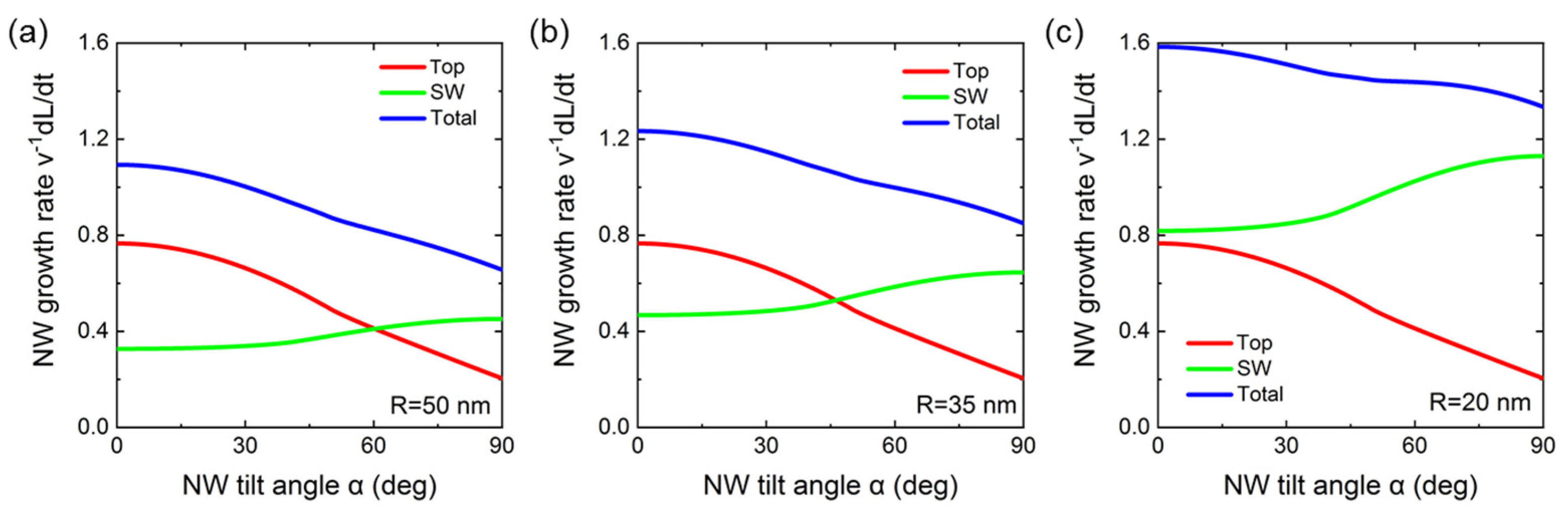
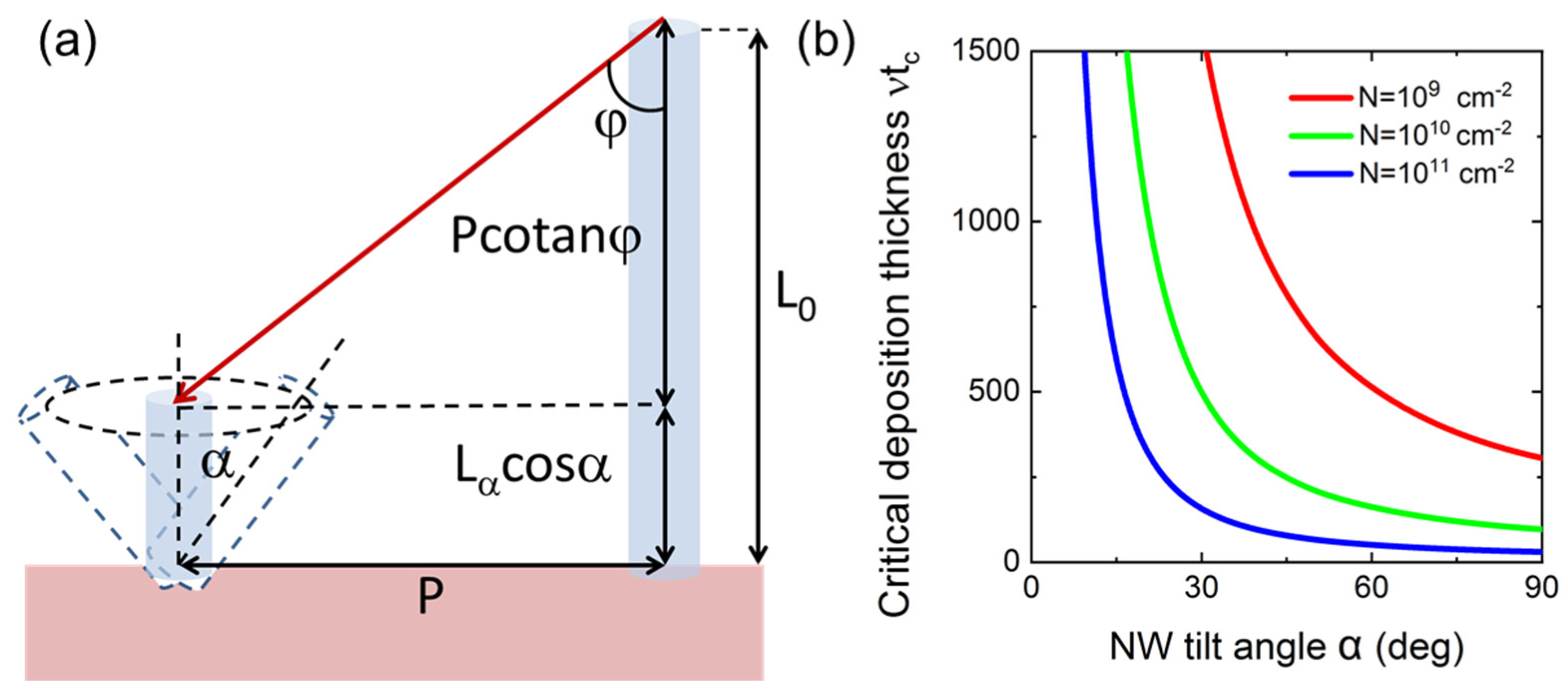
Figures 6 show the contributions into the NW axial growth rate originating from the direct impingement onto the top facet and surface diffusion of Ga adatoms from the NW sidewalls at a fixed 40 nm and three different different NW radii 20 nm, 35 nm (corresponing to the average radius of GaN NWs in Figure 2), and 50 nm. The diffusion-induced axial growth rate increases and the direct impingement term decreases with the NW tilt angle, as in Figure 5 (d). The diffusion-indiced contribution becomes greater for smaller NW radii. This leads to a steeper decrease of the total NW growth rate for larger NW radii. In all cases, the total axial growht rate decreases with the NW titl angle, which is why more inclined NWs grow slower than less inclined NWs. At 35 nm, the axial growth rate of in-plane NWs decreases by approximately 30% with respect to the maximum growth rate of vertical NWs. The effective height of inclined NWs having the tilt angle above the substrate surface, is given by (see Figure 7 (a)). Therefore, the longest vertically aligned NWs with will shadow the shorter inclined NWs in ther course of MBE growth, leading to the geometrical selection of vertical NWs after a certain time. The shadowing effect should be enhanced in dense ensembles of NWs.
Figure 6.
Total axial NW growth rates in the units of , deconvoluted into the contributions of the top and sidewall (SW) facets versus the NW tilt angle. The curves are obtained from Eq. (1) at a fixed Ga diffusion length =40 nm and φ=40o for different NW radii: (a) 50 nm, (b) 35 nm, and (c) 20 nm. In all cases, the total axial growth rate decreases with . The decrease is steeper for larger NW radii.
To describe the effect of geometrical selection of vertically aligned NWs in MBE growth with substrate rotation, we consider the geometrical shadowing of a given NW by the neighboring NWs [43,44]. A NW with the tilt angle gets fully shadowed by the longest vertical NWs when Ga atoms can no longer impinge onto its top surface and side facets. According to Figure 7 (a), this occurs when
where is the average distance between the NWs, is their surface density and is a shape constant in the order of unity. Both and are proportional to the actual NW growth time and . Here, is the dependent geometrical function shown in Figure 6 for 35 nm, which describes the axial growth suppression with increasing the tilt angle . Using these expressions, the critical NW growth time correspoding to the full shadowing of NWs with the tilt angle , , is obtained in the form
This simple expression shows that the critical time for the full shadowing of NWs (i) decreases with the Ga beam angle , (ii) decreases for higher NW density , and (iii) decreases for larger NW tilt angles . The latter property is due to (i) corresponing to a slower axial growth rate of inclined NWs, and (ii) the presence of in the denominator of Equation (7) describing the reduced height of inclined NWs above the substrate surface which decreases for more inclined NW and equals zero for planar NWs with 90o.
Figure 7 (b) shows the effective deposition thickness of GaN as a function of the NW tilt angle, obtained from Equation (7) at three different NW surface densities of 109 cm-2, 1010 cm-2 and 1011 cm-2 (corresponing to the highest NW density in Figure 2 and Figure 4 (d)). It is seen that gradually decreses with and . A larger suppression of more inclined GaN NWs at higher NW surface densities is confirmed by our experimental data shown in Figures 4. A more qualitative analysis of the effect of geometrical selection of vertically aligned GaN NWs in MBE growth as a function of the NW growth time and other technologically controlled parameters requires more studies and will be presented elswhere.
4. Conclusions
To summarize, we have studied the morphology of GaN NWs grown by PAMBE on polycrystalline ZrN buffer layers. Our results lead to the following scenario of PAMBE growth of GaN NWs epitaxially linked to grains of the polycrystalline ZrN buffer. The NWs nucleate with random orientations induced by the metallic grains. The axial growth rate is highest for vertically aligned NWs, and decreases with increasing the NW tilt angle with respect to the substrate normal. At the beginning, the NWs continue to grow with random orientations as nucleated. At a certain stage, the effect of preferential growth induced by unidirectional supply of Ga in MBE starts to dominate. Fast growing NWs with smaller tilt angles shadow the more tilted ones that grow slower. In this way, the NWs nearly perpendicular to the substrate surface are geometrically selected and survive in the entire NW ensemble. After a given growth time, the effect of geometrical selection of vertically aligned NWs is more pronounced for higher NW surface densities, which enabled us to obtain the application-relevant dense ensembles of nearly vertical GaN NWs. Overall, we have demonstrated that the geometry of MBE growth helps to overcompensate random orientation of the initial GaN NWs induced by arbitrary arrangement of substrate grains. The effect of geometrical selection of vertically aligned NWs in the directional MBE technique is quite general and should be present in different material systems where NWs nucleate with random orientations induced by the surface grains.
Acknowledgments
This work was partially supported by the NCN grants 2021/43/D/ST7/01936 and 2022/04/Y/ST7/00043. The authors thank Z. Szopniewski for depositing ZrN layers. A. Reszka, A. Pieniążek and A. Lysak are acknowledged for SEM measurements of the samples. VGD and EDL gratefully acknowledge financial support of the modeling part of the work by the research grant of St. Petersburg State University (ID 94033852).
References
- Ristić, J.; Calleja, E.; Fernández-Garrido, S.; Cerutti, L.; Trampert, A.; Jahn, U.; Ploog, K.H. On the Mechanisms of Spontaneous Growth of III-Nitride Nanocolumns by Plasma-Assisted Molecular Beam Epitaxy. Journal of Crystal Growth 2008, 310, 4035–4045. [Google Scholar] [CrossRef]
- Glas, F. Critical Dimensions for the Plastic Relaxation of Strained Axial Heterostructures in Free-Standing Nanowires. Phys. Rev. B 2006, 74, 121302. [Google Scholar] [CrossRef]
- Sun, H.; Li, X. Recent Advances on III-Nitride Nanowire Light Emitters on Foreign Substrates – Toward Flexible Photonics. Physica Status Solidi (a) 2019, 216, 1800420. [Google Scholar] [CrossRef]
- Carnevale, S.D.; Yang, J.; Phillips, P.J.; Mills, M.J.; Myers, R.C. Three-Dimensional GaN/AlN Nanowire Heterostructures by Separating Nucleation and Growth Processes. Nano Lett. 2011, 11, 866–871. [Google Scholar] [CrossRef] [PubMed]
- Calarco, R.; Meijers, R.J.; Debnath, R.K.; Stoica, T.; Sutter, E.; Lüth, Hans. Nucleation and Growth of GaN Nanowires on Si(111) Performed by Molecular Beam Epitaxy. Nano Lett. 2007, 7, 2248–2251. [Google Scholar] [CrossRef] [PubMed]
- Consonni, V.; Knelangen, M.; Geelhaar, L.; Trampert, A.; Riechert, H. Nucleation Mechanisms of Epitaxial GaN Nanowires: Origin of Their Self-Induced Formation and Initial Radius. Phys. Rev. B 2010, 81, 085310. [Google Scholar] [CrossRef]
- Park, Y.S.; Lee, S.-H.; Oh, J.-E.; Park, C.-M.; Kang, T.-W. Self-Assembled GaN Nano-Rods Grown Directly on (111) Si Substrates: Dependence on Growth Conditions. Journal of Crystal Growth 2005, 282, 313–319. [Google Scholar] [CrossRef]
- Bertness, K.A.; Roshko, A.; Sanford, N.A.; Barker, J.M.; Davydov, A.V. Spontaneously Grown GaN and AlGaN Nanowires. Journal of Crystal Growth 2006, 287, 522–527. [Google Scholar] [CrossRef]
- Consonni, V.; Hanke, M.; Knelangen, M.; Geelhaar, L.; Trampert, A.; Riechert, H. Nucleation Mechanisms of Self-Induced GaN Nanowires Grown on an Amorphous Interlayer. Phys. Rev. B 2011, 83, 035310. [Google Scholar] [CrossRef]
- Zhao, S.; Kibria, M.G.; Wang, Q.; Nguyen, H.P.T.; Mi, Z. Growth of Large-Scale Vertically Aligned GaN Nanowires and Their Heterostructures with High Uniformity on SiOx by Catalyst-Free Molecular Beam Epitaxy. Nanoscale 2013, 5, 5283–5287. [Google Scholar] [CrossRef]
- Stoica, T.; Sutter, E.; Meijers, R.J.; Debnath, R.K.; Calarco, R.; Lüth, H.; Grützmacher, D. Interface and Wetting Layer Effect on the Catalyst-Free Nucleation and Growth of GaN Nanowires. Small 2008, 4, 751–754. [Google Scholar] [CrossRef] [PubMed]
- Sobanska, M.; Fernández-Garrido, S.; Zytkiewicz, Z.R.; Tchutchulashvili, G.; Gieraltowska, S.; Brandt, O.; Geelhaar, L. Self-Assembled Growth of GaN Nanowires on Amorphous AlxOy: From Nucleation to the Formation of Dense Nanowire Ensembles. Nanotechnology 2016, 27, 325601. [Google Scholar] [CrossRef] [PubMed]
- Sobanska, M.; Korona, K.P.; Zytkiewicz, Z.R.; Klosek, K.; Tchutchulashvili, G. Kinetics of Self-Induced Nucleation and Optical Properties of GaN Nanowires Grown by Plasma-Assisted Molecular Beam Epitaxy on Amorphous AlxOy. Journal of Applied Physics 2015, 118, 184303. [Google Scholar] [CrossRef]
- Sobanska, M.; Zytkiewicz, Z.R.; Calabrese, G.; Geelhaar, L.; Fernández-Garrido, S. Comprehensive Analysis of the Self-Assembled Formation of GaN Nanowires on Amorphous AlxOy: In Situ Quadrupole Mass Spectrometry Studies. Nanotechnology 2019, 30, 154002. [Google Scholar] [CrossRef] [PubMed]
- Janjua, B.; Sun, H.; Zhao, C.; Anjum, D.H.; Wu, F.; Alhamoud, A.A.; Li, X.; Albadri, A.M.; Alyamani, A.Y.; El-Desouki, M.M.; et al. Self-Planarized Quantum-Disks-in-Nanowires Ultraviolet-B Emitters Utilizing Pendeo-Epitaxy. Nanoscale 2017, 9, 7805–7813. [Google Scholar] [CrossRef]
- Sarwar, A.G.; Carnevale, S.D.; Yang, F.; Kent, T.F.; Jamison, J.J.; McComb, D.W.; Myers, R.C. Semiconductor Nanowire Light-Emitting Diodes Grown on Metal: A Direction Toward Large-Scale Fabrication of Nanowire Devices. Small 2015, 11, 5402–5408. [Google Scholar] [CrossRef]
- Wölz, M.; Hauswald, C.; Flissikowski, T.; Gotschke, T.; Fernández-Garrido, S.; Brandt, O.; Grahn, H.T.; Geelhaar, L.; Riechert, H. Epitaxial Growth of GaN Nanowires with High Structural Perfection on a Metallic TiN Film. Nano Lett. 2015, 15, 3743–3747. [Google Scholar] [CrossRef]
- May, B.J.; Sarwar, A.T.M.G.; Myers, R.C. Nanowire LEDs Grown Directly on Flexible Metal Foil. Applied Physics Letters 2016, 108, 141103. [Google Scholar] [CrossRef]
- Calabrese, G.; Corfdir, P.; Gao, G.; Pfüller, C.; Trampert, A.; Brandt, O.; Geelhaar, L.; Fernández-Garrido, S. Molecular Beam Epitaxy of Single Crystalline GaN Nanowires on a Flexible Ti Foil. Applied Physics Letters 2016, 108, 202101. [Google Scholar] [CrossRef]
- Zhao, C.; Ng, T.K.; Wei, N.; Prabaswara, A.; Alias, M.S.; Janjua, B.; Shen, C.; Ooi, B.S. Facile Formation of High-Quality InGaN/GaN Quantum-Disks-in-Nanowires on Bulk-Metal Substrates for High-Power Light-Emitters. Nano Lett. 2016, 16, 1056–1063. [Google Scholar] [CrossRef]
- Calabrese, G.; Pettersen, S.V.; Pfüller, C.; Ramsteiner, M.; Grepstad, J.K.; Brandt, O.; Geelhaar, L.; Fernández-Garrido, S. Effect of Surface Roughness, Chemical Composition, and Native Oxide Crystallinity on the Orientation of Self-Assembled GaN Nanowires on Ti Foils. Nanotechnology 2017, 28, 425602. [Google Scholar] [CrossRef] [PubMed]
- Calabrese, G.; Gao, G.; Treeck, D. van; Corfdir, P.; Sinito, C.; Auzelle, T.; Trampert, A.; Geelhaar, L.; Brandt, O.; Fernández-Garrido, S. Interfacial Reactions during the Molecular Beam Epitaxy of GaN Nanowires on Ti/Al2O3. Nanotechnology 2019, 30, 114001. [Google Scholar] [CrossRef] [PubMed]
- Mudiyanselage, K.; Katsiev, K.; Idriss, H. Effects of Experimental Parameters on the Growth of GaN Nanowires on Ti-Film/Si(100) and Ti-Foil by Molecular Beam Epitaxy. Journal of Crystal Growth 2020, 547, 125818. [Google Scholar] [CrossRef]
- Auzelle, T.; Azadmand, M.; Flissikowski, T.; Ramsteiner, M.; Morgenroth, K.; Stemmler, C.; Fernández-Garrido, S.; Sanguinetti, S.; Grahn, H.T.; Geelhaar, L.; et al. Enhanced Radiative Efficiency in GaN Nanowires Grown on Sputtered TiNx: Effects of Surface Electric Fields. ACS Photonics 2021, 8, 1718–1725. [Google Scholar] [CrossRef]
- Calabrese, G.; Gao, G.; Treeck, D. van; Corfdir, P.; Sinito, C.; Auzelle, T.; Trampert, A.; Geelhaar, L.; Brandt, O.; Fernández-Garrido, S. Interfacial Reactions during the Molecular Beam Epitaxy of GaN Nanowires on Ti/Al2O3. Nanotechnology 2019, 30, 114001. [Google Scholar] [CrossRef]
- Heying, B.; Averbeck, R.; Chen, L.F.; Haus, E.; Riechert, H.; Speck, J.S. Control of GaN Surface Morphologies Using Plasma-Assisted Molecular Beam Epitaxy. Journal of Applied Physics 2000, 88, 1855–1860. [Google Scholar] [CrossRef]
- Klosek, K.; Sobanska, M.; Tchutchulashvili, G.; Zytkiewicz, Z.R.; Teisseyre, H.; Klopotowski, L. Optimization of Nitrogen Plasma Source Parameters by Measurements of Emitted Light Intensity for Growth of GaN by Molecular Beam Epitaxy. Thin Solid Films 2013, 534, 107–110. [Google Scholar] [CrossRef]
- Colombi, P.; Zanola, P.; Bontempi, E.; Roberti, R.; Gelfi, M.; Depero, L.E. Glancing-Incidence X-Ray Diffraction for Depth Profiling of Polycrystalline Layers. J Appl Cryst 2006, 39, 176–179. [Google Scholar] [CrossRef]
- Langford, J.I.; Wilson, A.J.C. Scherrer after Sixty Years: A Survey and Some New Results in the Determination of Crystallite Size. J Appl Cryst 1978, 11, 102–113. [Google Scholar] [CrossRef]
- de Keijser, T.; Mittemeijer, E.J.; Rozendaal, H.C.F. The Determination of Crystallite-Size and Lattice-Strain Parameters in Conjunction with the Profile-Refinement Method for the Determination of Crystal Structures. J Appl Cryst 1983, 16, 309–316. [Google Scholar] [CrossRef]
- Sobanska, M.; Wierzbicka, A.; Klosek, K.; Borysiuk, J.; Tchutchulashvili, G.; Gieraltowska, S.; Zytkiewicz, Z.R. Arrangement of GaN Nanowires Grown by Plasma-Assisted Molecular Beam Epitaxy on Silicon Substrates with Amorphous Al2O3 Buffers. Journal of Crystal Growth 2014, 401, 657–660. [Google Scholar] [CrossRef]
- Foxon, C.T.; Novikov, S.V.; Hall, J.L.; Campion, R.P.; Cherns, D.; Griffiths, I.; Khongphetsak, S. A Complementary Geometric Model for the Growth of GaN Nanocolumns Prepared by Plasma-Assisted Molecular Beam Epitaxy. Journal of Crystal Growth 2009, 311, 3423–3427. [Google Scholar] [CrossRef]
- Wierzbicka, A.; Zytkiewicz, Z.R.; Kret, S.; Borysiuk, J.; Dluzewski, P.; Sobanska, M.; Klosek, K.; Reszka, A.; Tchutchulashvili, G.; Cabaj, A.; et al. Influence of Substrate Nitridation Temperature on Epitaxial Alignment of GaN Nanowires to Si(111) Substrate. Nanotechnology 2012, 24, 035703. [Google Scholar] [CrossRef] [PubMed]
- Sanchez-Garcia, M. A.; Calleja, E.; Monroy, E.; Sanchez, F. J.; Calle, F.; Muñoz, E.; Beresford, R. J. The effect of the III/V ratio and substrate temperature on the morphology and properties of GaN- and AlN-layers grown by molecular beam epitaxy on Si(1 1 1). J. Cryst. Growth 1998, 183, 23. [Google Scholar] [CrossRef]
- Debnath, R. K.; Meijers, R.; Richter, T.; Stoica, T.; Calarco, R.; Lüth. H. Mechanism of molecular beam epitaxy growth of GaN nanowires on Si. Appl. Phys. Lett. 2007, 90, 123117. [Google Scholar] [CrossRef]
- Galopin, E.; Largeau, L.; Patriarche, G.; Travers, L.; Glas, F.; Harmand, J. C. Morphology of self-catalyzed GaN nanowires and chronology of their formation by molecular beam epitaxy. Nanotechnology 2011, 22, 245606. [Google Scholar] [CrossRef]
- Songmuang, R.; Ben, T.; Daudin, B.; Gonzalez, D.; Monroy, E. Identification of III–N nanowire growth kinetics via a marker technique. Nanotechnology 2010, 21, 295605. [Google Scholar] [CrossRef]
- Dubrovskii, V. G.; Consonni, V.; Geelhaar, L.; Trampert, A.; Riechert. H. Scaling growth kinetics of self-induced GaN nanowires. Appl. Phys. Lett. 2012, 100, 153101. [Google Scholar] [CrossRef]
- Consonni, V.; Dubrovskii, V. G.; Trampert, A.; Geelhaar, L.; Riechert, H. Quantitative description for the growth rate of self-induced GaN nanowires. Phys. Rev. B 2012, 85, 155313. [Google Scholar] [CrossRef]
- Sobanska, M.; Dubrovskii, V. G.; Tchutchulashvili, G.; Klosek, K.; Zytkiewicz, Z. R. Analysis of incubation times for the self-induced formation of GaN nanowires: influence of the substrate on the nucleation mechanism. Cryst. Growth Des. 2016, 16, 7205. [Google Scholar] [CrossRef]
- Cirlin, G. E.; Dubrovskii, V. G.; Sibirev, N. V.; Soshnikov, I. P.; Samsonenko, Yu. B.; Tonkikh, A. A.; Ustinov, V. M. The diffusion mechanism in the formation of GaAs and AlGaAs nanowhiskers during the process of molecular-beam epitaxy. Semiconductors 2005, 39, 557. [Google Scholar] [CrossRef]
- Zhang, X.; Dubrovskii, V. G.; Sibirev, N. V.; Cirlin, G. E.; Sartel, C.; Tchernycheva, M.; Harmand, J. C.; Glas, F. Growth of inclined GaAs nanowires by molecular beam epitaxy: theory and experiment. Nanoscale Res. Lett. 2010, 5, 1692. [Google Scholar] [CrossRef] [PubMed]
- Sibirev, N. V.; Tchernycheva, M.; Timofeeva, M. A.; Harmand, J. C.; Cirlin, G. E.; Dubrovskii, V. G. Influence of shadow effect on the growth and shape of InAs nanowires. J. Appl. Phys. 2012, 111, 104317. [Google Scholar] [CrossRef]
- Koivusalo, E.; Hakkarainen, T.; Guina, M. D.; Dubrovskii, V. G. Sub-Poissonian narrowing of length distributions realized in Ga-catalyzed GaAs nanowires. Nano Lett. 2017, 17, 5350. [Google Scholar] [CrossRef] [PubMed]
Figure 1.
(a) θ/2θ X-ray diffraction scan and (b) GIXRD scan of ZrN polycrystalline film on Si(111) substrate.
Figure 1.
(a) θ/2θ X-ray diffraction scan and (b) GIXRD scan of ZrN polycrystalline film on Si(111) substrate.
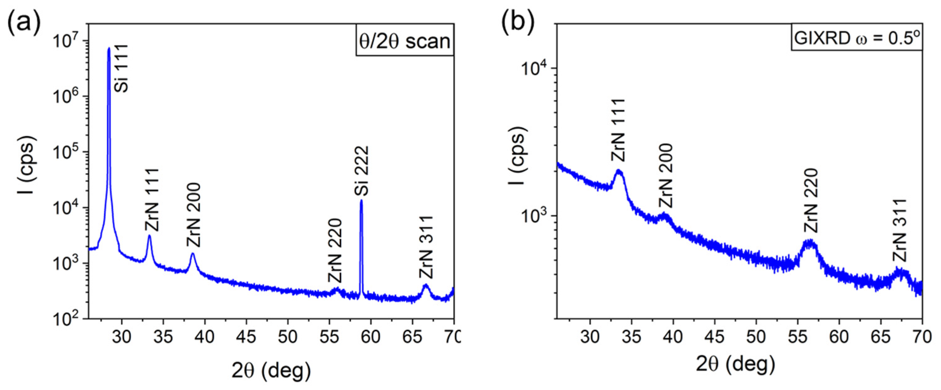
Figure 2.
(a) SEM image of GaN NWs grown on ZrN buffer. The NWs are mostly oriented along the substrate normal. (b) Small GaN crystallites between the NWs.
Figure 2.
(a) SEM image of GaN NWs grown on ZrN buffer. The NWs are mostly oriented along the substrate normal. (b) Small GaN crystallites between the NWs.
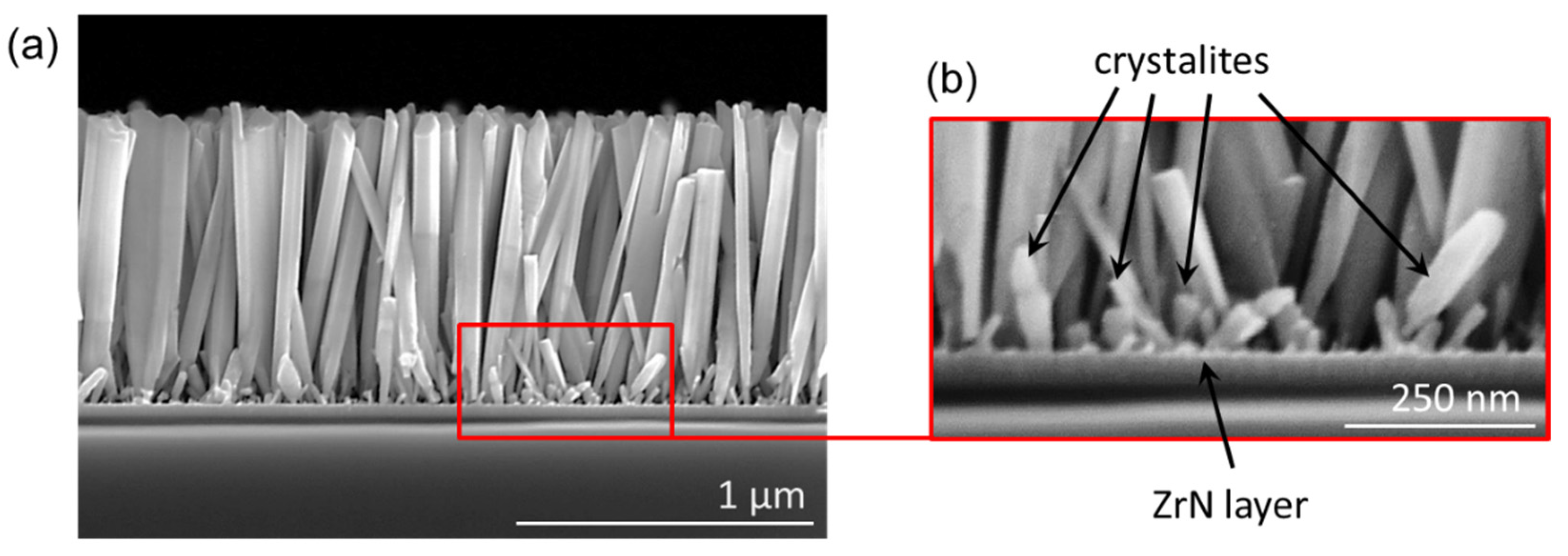
Figure 3.
SEM image of GaN NWs grown on ZrN buffer without substrate rotation. The sample was cleaved in the plane defined by the normal to the substrate and the line-of-sight of the Ga source. The dashed line shows the Ga beam direction in the MBE system.
Figure 3.
SEM image of GaN NWs grown on ZrN buffer without substrate rotation. The sample was cleaved in the plane defined by the normal to the substrate and the line-of-sight of the Ga source. The dashed line shows the Ga beam direction in the MBE system.
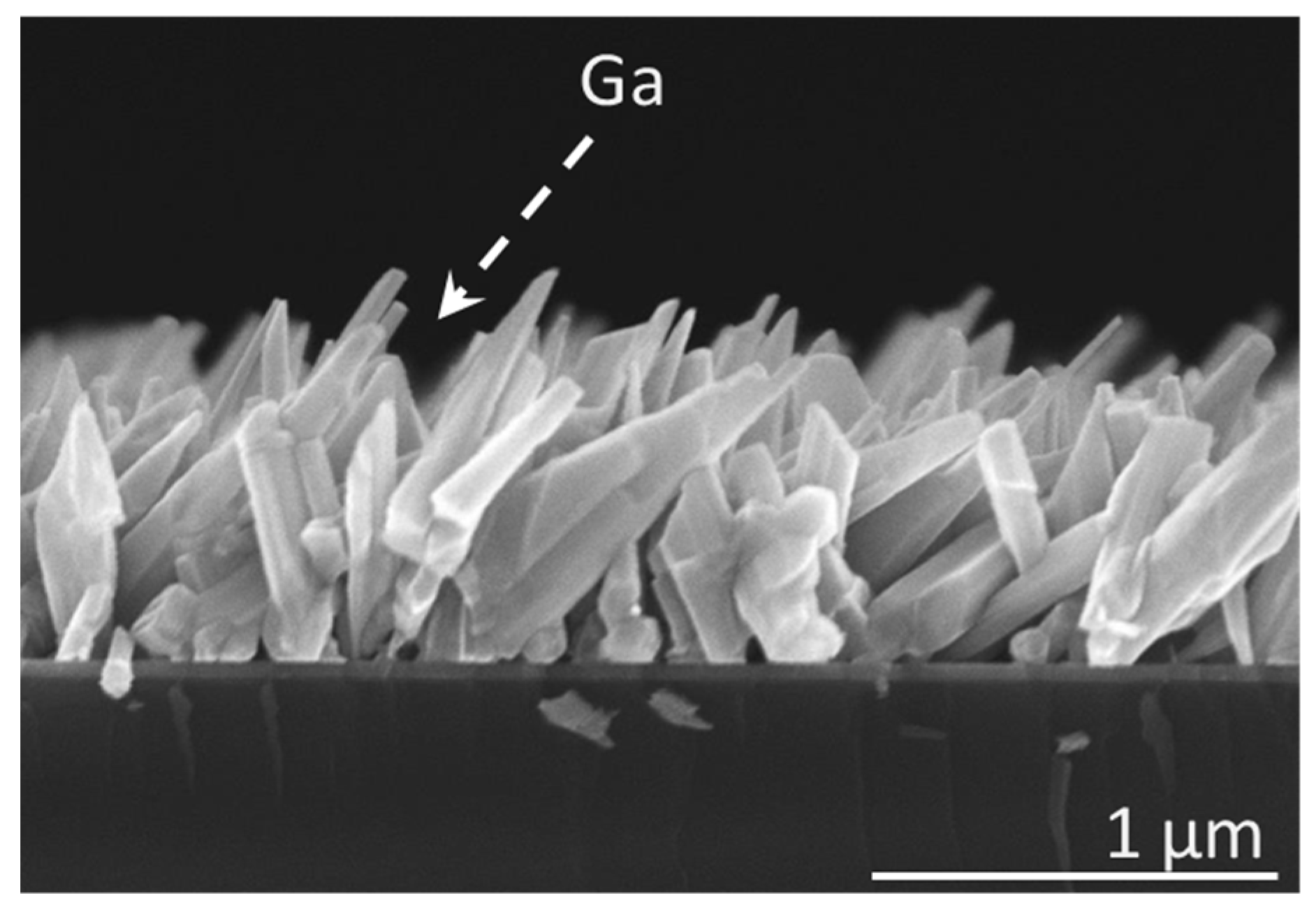
Figure 4.
(a – d) SEM images of different parts of GaN NW sample with increasing NW density, (e) shows the FWHM values of XRD ω-scan representing the tilt dispersion of the NW ensemble at the respective parts of the sample.
Figure 4.
(a – d) SEM images of different parts of GaN NW sample with increasing NW density, (e) shows the FWHM values of XRD ω-scan representing the tilt dispersion of the NW ensemble at the respective parts of the sample.
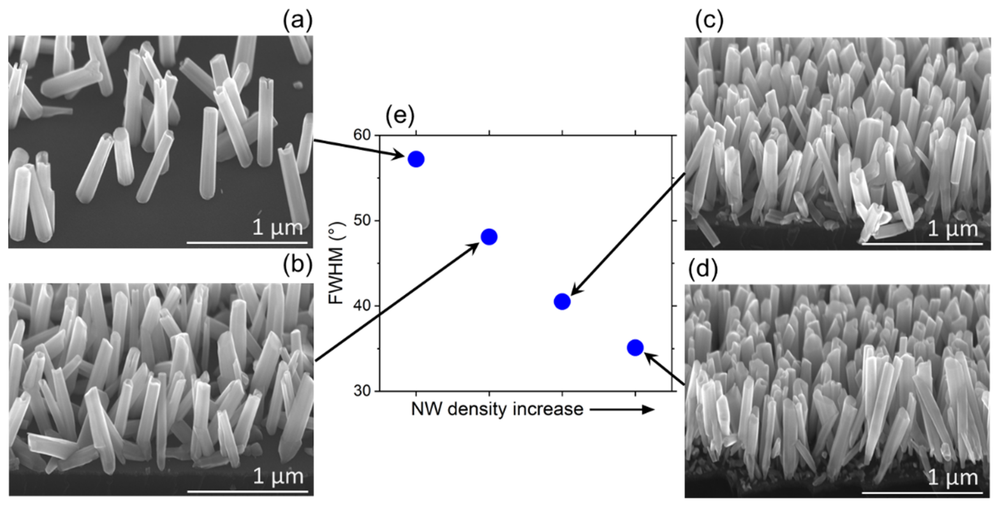
Figure 5.
(a) Illustration of MBE growth of an inclined NW with the tilt angle , from a Ga beam with the angle 40o; denotes the angle related to substrate rotation. Effective area of (b) the NW top facet and (c) NW sidewalls as a function of α and ω at a fixed 40o. (d) Normalized contributions of the top and sidewall (SW) facets into the total axial growth rate versus the NW tilt angle at 40o. Numerical solutions are obtained by summing up the elements of the contour plots of (b) and (c) over ω at a fixed α and dividing the result by the number of elements. Analytical solutions are obtained from Equations (2) to (4). The approximate solution is obtained using Equation (5).
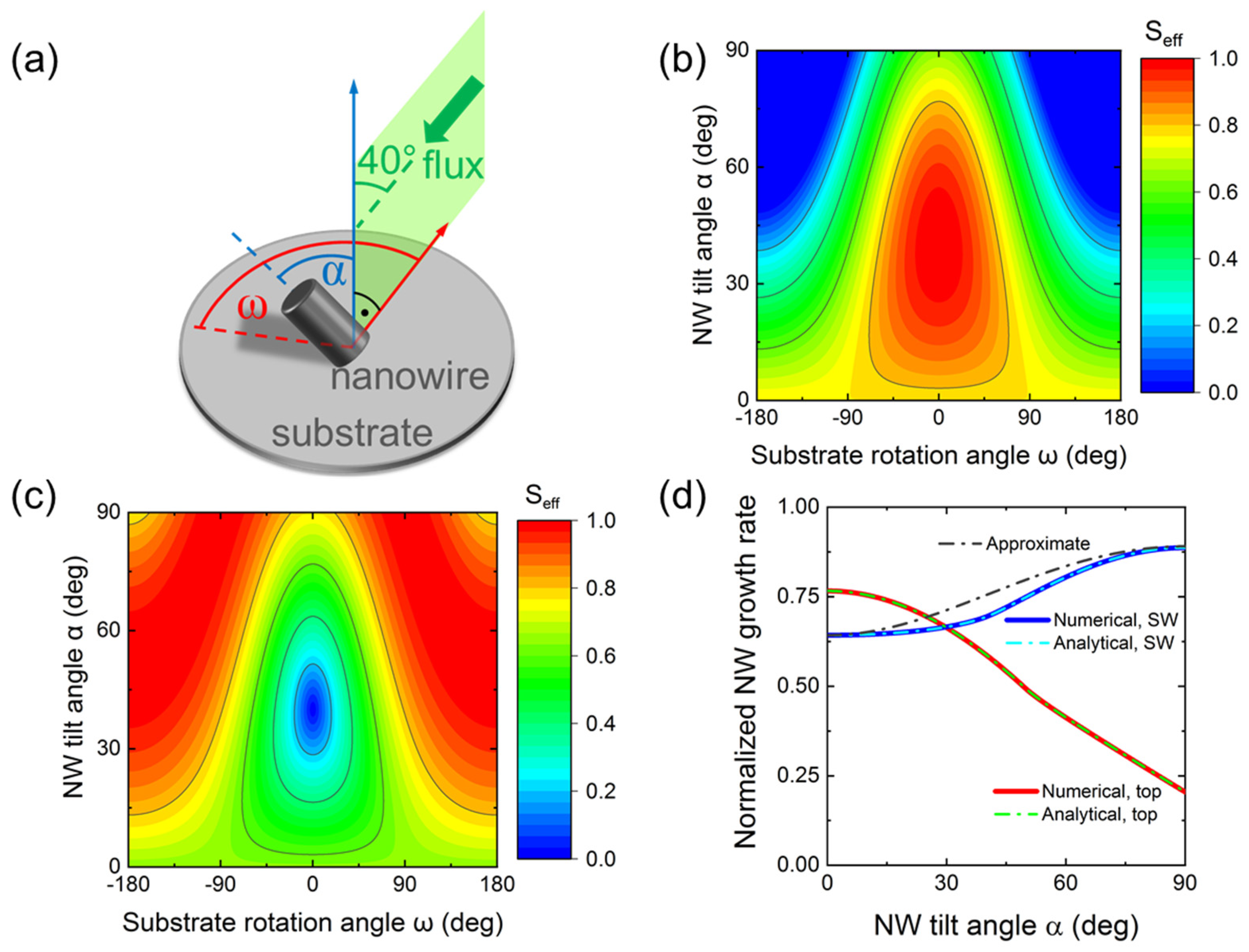
Figure 7.
(a) Illustration of the geometrical shadowing effect on a NW with the tilt angle , originating from the circle of neighboring vertical NWs. Rotating substrate does not influence the height of vertical NWs , but reduces the effective height of inclined NW to because, for each rotation angle , the full length is partly shadowed by one vertical NW in a circle. The average distance between the NWs equals . From geometrical consideration, the full shadowing of a given NW occurs when its height plus equals the length of vertical NWs. (b) Critical deposition thickness of GaN as a function of the NW tilt angle at a fixed40o and three different NW densities given in the legend. The critical time at which all the NWs having the tilt angle stop growing strongly decreases with and . Therefore, more inclined NWs stop growing faster, and finally only vertically alligned NWs survive in the whole NW ensemble.
Disclaimer/Publisher’s Note: The statements, opinions and data contained in all publications are solely those of the individual author(s) and contributor(s) and not of MDPI and/or the editor(s). MDPI and/or the editor(s) disclaim responsibility for any injury to people or property resulting from any ideas, methods, instructions or products referred to in the content. |
© 2023 by the authors. Licensee MDPI, Basel, Switzerland. This article is an open access article distributed under the terms and conditions of the Creative Commons Attribution (CC BY) license (http://creativecommons.org/licenses/by/4.0/).
Copyright: This open access article is published under a Creative Commons CC BY 4.0 license, which permit the free download, distribution, and reuse, provided that the author and preprint are cited in any reuse.


