Preprint
Article

Structural Inhomogeneities and Nonlinear Phenomena in Charge Transfer under Cold Field Emission in Individual Closed Carbon Nanotubes

Altmetrics

Downloads

129

Views

47

Comments

0

A peer-reviewed article of this preprint also exists.

Submitted:

27 July 2023

Posted:

28 July 2023

You are already at the latest version

Alerts
Abstract
The structure and phenomena arising from charge transfer in cold field emission modus in a single closed carbon nanotube under cold field emission conditions were studied. By studying microphotographs in various microscopes - AFM, SEM, TEM it was found inhomogeneities in the form of two types of superlattices. The conductivity of the emitter section of a nanodiode circuit with an emitter made of an individual closed carbon nanotube (CNT) and arrays of closed CNTs was studied. High values of cold field emission were observed, as well as nonlinearity and anomalies of the current-voltage characteristic (I-V characteristics), which manifested themselves in the form of peaks at low and high current values. Peaks in the CVC have distinct areas of negative differential conductivity. It is argued, that the anomalously high currents in the I–V characteristics of cold field emission of electrons from a nanoemitter made of closed CNTs can be associated with a sharp increase in the density of electron states at energies near the van Hove singularity.
Keywords: 
Subject: Physical Sciences  -   Condensed Matter Physics

1. Introduction

Experimentally, carbon nanotubes (CNTs) were discovered in 1991 by Iijima [1] and almost simultaneously and independently in [2,3]. First, CNT were discovered as the multiwalled carbon nanotubes (MWCNTs). The existence of single-walled carbon nanotubes (SWCNTs) was experimentally proved in 1993 [4,5]. Cold field emission (CFE) from carbon nanotubes was discovered [6] and after this was widely studied, see, for example reviews [7,8] and literature cited there. CFE phenomenon is very interesting from the point of view of fundamental science, and attracts permanent interest of researchers [6,7,8,9,10,11]. CFE from CNTs makes it possible to study the features of the work function and features of transport under field emission conditions for individual 1D object and their arrays. The individual CNTs, are actually large single molecules, demonstrating field emission in the case of ballistic transport [12,13], see review [14] and the literature cited there.
CFE from CNTs is also of great practical interest, since high-efficiency cathodes can be created on the basis of CNTs, which open up the possibility of developing a new generation of the microwave and THz components for micro- and nano- solid state and vacuum electronics, including generators, detectors etc. [7,8,14,15,16,17,18,19] and also the review [20]. The emission of single electrons from individual CNTs makes it possible to create the single-electron devices, which are necessary for quantum technologies [21]. The miniature X-ray sources based on CNTs have also been created [7,8,23,24,25,26].
The cathodoluminescence from CNTs in the optical range is observed [27]. On the basis of cathodoluminescence, it is possible to create both conventional light sources and flexible screens. It is also suggested [28,29,30,31,32] that CNT-based probes for different scanning microscope, like atomic force (AFM) [28] scanning tunneling microscopy (STM) [29,30,31] can be created. Such microscopes due to the high density of the emission current and the small size of the emission region, make it possible to increase the spatial resolution and image brightness. The CNT size gives the possibility to scan deep and narrow depressions in the sample relief, which is impossible for conventional probes [28,29]. The next application are vacuum meters based on CNTs [33].
Could field emission performance of a single isolated CNT can be evaluated as remarkable. This is due to structural integrity, high thermal conductivity and geometry of the CNTs. It should be noted that it is the possible in principle to miniaturize all devices based on cold field emission using CNTs. Many advantages of CNT-based cathodes are due to the high aspect ratio of CNTs, consequently the electric field strength in the vicinity of the CNT tip can be hundreds of times higher than the volume-average electric field strength generated by an external source. Another important advantage of CNTs is their chemical inertness and high mechanical strength. CNT-based cathodes have high efficiency, including energy efficiency and short turn-on time. However, field cathodes based on CNTs also have a number of disadvantages, the main of which is their fragility.
Despite of great interest and numerous studies, there is still no complete understanding of the mechanism of cold field emission from CNTs. The main theory of CFE from CNTs, as well as field emission from the metals, is the Fowler-Nordheim theory (F-NT), which was developed for bulk metal cathodes [22], and its various modifications [7,8,35,36,37,38].
However, many experiments [7,8] show deviations from this theory in the case of some of the phenomena observed during cold field emission CNTs. F-NT does not takes into account the real structural features of nanotubes: the size on nanometer scale, chirality, surface features, the presence of "lids", defects, adsorption of various substances, etc.
The first studies of field emission from CNTs showed anomalously low voltages at which field emission is observed [6,7,8]. The emission currents were one or two orders of magnitude higher than it follows from the F-NT equation [35,36,37,38,39,40]. That is, the fundamental question of the nature of the field emission from CNTs remains relevant, without solving which it is practically impossible to select the optimal structure and further develop cathodes and other devices from CNT.
This work is devoted to the experimental study of the I–V characteristics of nanodiodes from closed CNTs and special features of CNT, i. e. structure, which can effect the CFE, with the aim to clarify the mechanism of CFE from individual CNTs.

2. Materials and Methods

Individual CNTs were prepared by deposition on wire electrodes made of tungsten, nickel and platinum using the arc technique (Figure 1a,b). Synthesis of oriented arrays of CNTs was carried out by chemical vapor deposition on a silicon substrate with deposited sublayers of aluminum and nickel, as described elsewhere [2,6]. As it is shown in [2,6], these CNTs are closed.
Experimental studies of the features of charge transfer were performed on the circuit of a nanotube emitter. The diode cell for measuring the emission characteristics of CNTs was assembled in a NEON 49 Carls Zeiss scanning electron microscope. This SEM is additionally equipped with an ion microscope column and Kleindiek micromanipulators with electrodes, as well as two SE-2 optical sensors with a spectral range from 1720 - 760 nm. The cathode emitters for the experiments were various single CNTs with the diameters from 2 to 14 nm and a length of about 1 μm. The acicular bulk cathode, in turn, was attached to the SEM table with a conductive paste. A pointed tungsten electrode-manipulator of a microscope with a diameter of ~0.5 mm sharpened to 100-200 nm served as the anode. The use of a micromanipulator made it possible to set the gap between the tungsten anode and the tip of the CNT emitter in the range from several hundred nm to 1 μm. (Figure 1a).
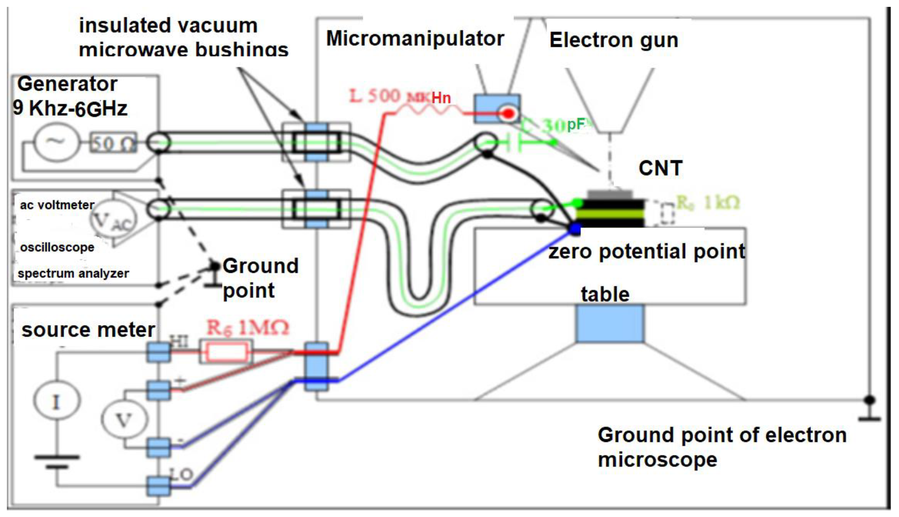
The scheme for measuring the current-voltage characteristics (I-V characteristic) of nanodiodes (see Figure 2) gives the possibility to reverse the signs on the electrodes and carry out measurements in the voltage sweep mode with a step of 0.02 V. In order to avoid a short circuit in the microscope chamber and heating of the electrodes, the scheme provided a voltage and a current limit. At micron gaps between the electrodes, the voltage did not exceed 30 V. At gaps of several tens microns, the voltage could be increased to 200 V. In any case, the current did not exceed 1 μA. If it was necessary, a current sweep could be carried out. The measured values of voltage and current were displayed on the screen in the form of current-voltage characteristics. Thus, we were able to track the change in current and the change in voltage between the CNT and the opposite electrode and, simultaneously, in an SEM, to observe all the changes occurring in the diode system. Electron-microscopic control of the electrode with CNTs and the opposite tungsten electrode was carried out before and after the measurement of the I-V characteristics.
I–V characteristics measurements in an electrostatic field were carried out with a voltage sweep with a step of 30 mV, which was set by a highly stable programmable Keithley 2400 source with an error no worse than + 5 μV. The measurements of direct emission current and voltage in the emitter circuit were carried out with an error of +10 pA and 1 μV, respectively.

3. Experimental studies of the structure of closed CNTs.

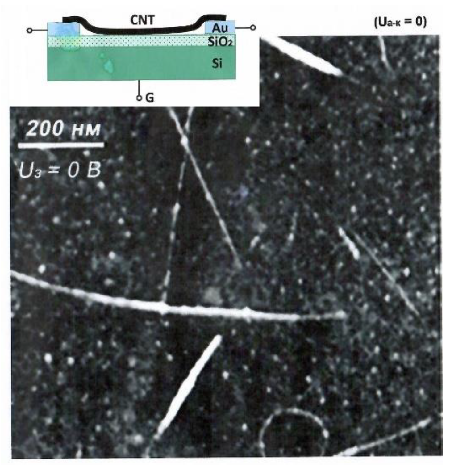
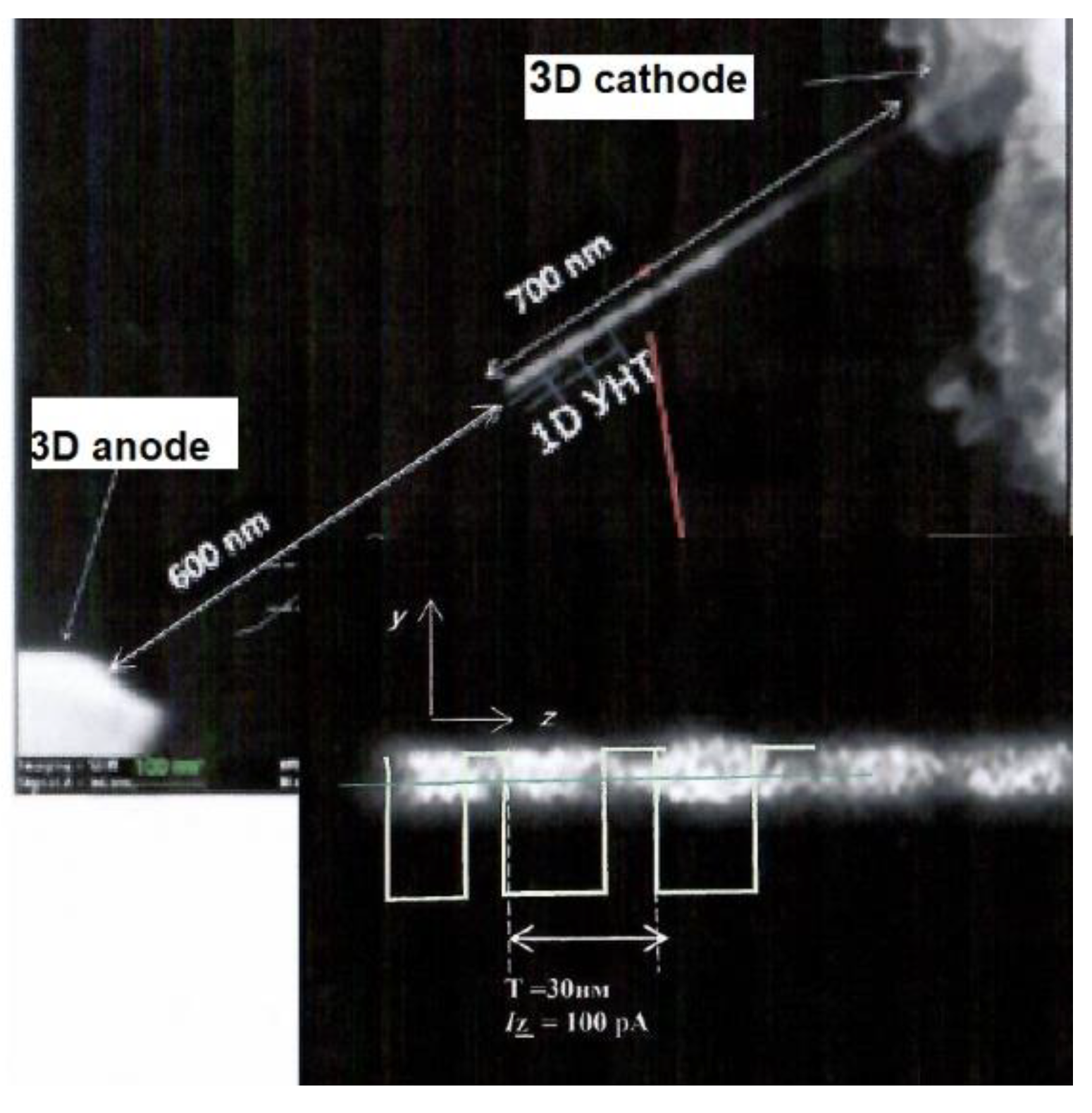
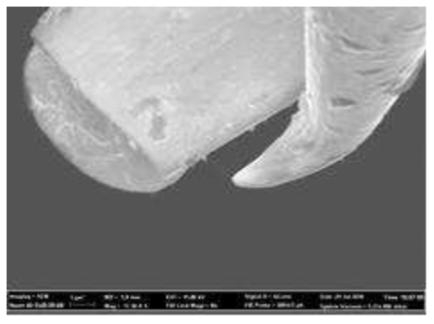
The structure of the samples of closed CNTs was studied in various microscopes – atomic force microscope (AFM), SEM, STM. Micrographs of diode structures of closed CNTs were obtained in AFM, SEM, STM for the diode circuit with CNT cathode, anode and vacuum gap for cold field emission. Structural inhomogeneities in closed CNTs were studied in situ under conditions of CFE for the diode measurement scheme shown in Figure 3, Figure 4, Figure 5 and Figure 6. During this study the external field was located both along the CNT and across it. The applied voltage diagram is given in the inset at the top of Figure 4.
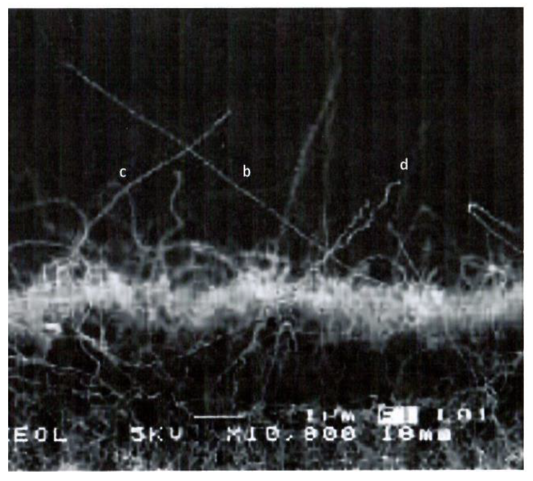
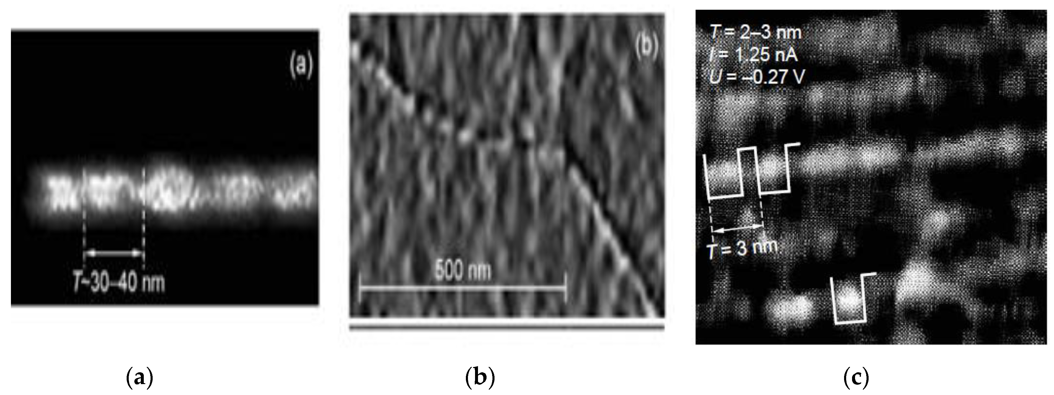
On the Figure 3 the micrographs are shown of CNT samples obtained in different microscopes. SEM image of CNTs with different types lattice deformations, defined with the letters “a”,”b”,”c”,”d”. On the Figure 4 the AFM is shown image of CNT superlattices, at E=0, Ug=0, the inset shows the scheme of voltage application to CNT. On the Figure 4 the results are shown of the study of the superlattices detected in single CNTs in SEM, AFM and STM. On 5 (a) it is shown the superlattice revealed in SEM image, with period about 30-40 nm. The emission current flows along the CNT. On the Figure 5 (b) one can see the AFM image of a CNT superlattice (period ~30–40 nm). The emission current also flows along the CNT. On the Figure 5 (c) it is shown STM micrograph of a superlattice in CNTs with period ~about 3 nm. The applied electric field is perpendicular to the CNT axis. On the Figure 6 it is shown SEM image of a nanodiode in secondary electrons.

4. Experimental results

4.1. Experimental studies of the structure of closed CNTs

On the Figure 3, Figure 4, Figure 5 and Figure 6 in microphotographs taken in AFM, SEM, STM the results are shown of some typical studies of structure of CNT. According to microphotographs, which was observed, that under CFE conditions in samples of closed CNTs, on a nanometer scale, there can be observed at least two different types of superlattices. Namely, a larger-scale superlattice arises when the current flows along the CNT axis (Figure 3, Figure 4, Figure 5 and Figure 6.). In these free-standing CNTs in the Figure 3, various types of deformation are clearly visible, denoted by the letters “a”,”b”,”c”,“d”. That is, these types of superlattices are caused by deformations of CNTs. This superlattice is probably caused by periodic deformation of the CNT walls and has a characteristic period of approximately 30–40 nm. The presence of a small-scale superlattice with a characteristic period of about 3 nm was also established by the STM method for the case when the field is applied perpendicular to the CNT axis. This type of superlattices is shown in Figure 5с and Figure 6.

4.2. Experimental studies of the features of charge transfer in the circuit of a nanotube emitter

On the Figure 7 it is shown the example of the SEM image of one of the studied diode structures with a single CNT deposited on a tungsten electrode.
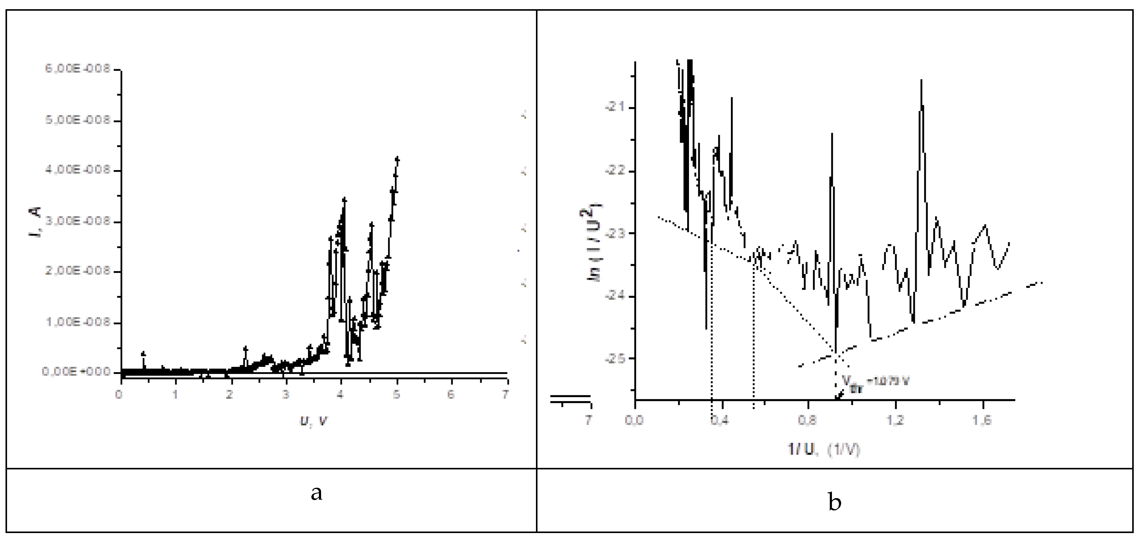
The CNT length was approximately 700 nm. In the experiments, the CNT diameter was about 14 nm. The distance between the tip of the nanotube and the tungsten counter electrode was at least 0.5 µm. Figure 8 (a, b) show the obtained I-V characteristics. The Figure 8(a) corresponds to the I-V characteristics graph plotted in I-V coordinates, and Figure 8(b) - in log(I/U2)-1/U coordinates, or Fowler-Nordheim coordinates. The dotted line is a straight line corresponding to the Fowler-Nordheim function. Based on these experimental data, the electron work function φ and the electric field gain at the tip of the free end of the nanotube β were estimated.

5. Discussion

Superlattices in CNTs have been theoretically and experimentally considered in many works, for example, [41,42,43,44]. In [41], the elastic free energy of CNTs grown by iron-catalyzed decomposition of acetylene was theoretically considered to provide the equilibrium shape of slightly curved CNTs. Equilibrium forms have been found for both stable and metastable cases. All found equilibrium forms are deformation superlattices, which were observed in the experiments of the authors of [41]. As suggested in this work, the deformations are caused by fluctuations in the growth conditions, such as pressure, temperature, and vapor composition. Also in our experiments, the results clearly show the presence of deformations along the CNT length. See Figure 3a, which could also be caused by growth conditions. Superlattices in an electric field perpendicular to the CNT axis were theoretically considered in [42]. In this paper, the motion of an electron in a CNT carbon nanotube (n, 1) is considered as a de Broglie wave propagating along a helix on the nanotube wall. It is theoretically shown that this motion leads to periodicity of the electron potential energy in the presence of an electric field normal to the nanotube axis, the period of this potential is proportional to the nanotube radius and greater than the interatomic distance in the nanotube. As a result, the behavior of an electron in an (n, 1) nanotube in a transverse electric field is similar to a semiconductor superlattice. That is, in this case, the size of the superlattice inhomogeneities observed in our experiments in a field perpendicular to the CNT axis coincides in order of magnitude with the inhomogeneities observed in our experiments.
Figure 8a and Figure 8b shows the CNT’s I-V characteristics in the course of the could field emission with resonance peaks. In general, the I-V characteristics has nonlinear character. The graphs clearly show the absence of the current saturation in the measurement region. The width of the resonant peaks increases with increasing applied voltage from several tens of millivolts to tens of volts. On the Fig 8 (b) it is shown the I-V characteristics in Fowler-Nordheim coordinates, and the threshold of the beginning of emission Uth is clearly visible. It is noted that the voltage sweep step is of decisive importance for the detection of I-V characteristics peaks. Thus, at a voltage sweep step of several millivolts, the first oscillation peak, the threshold for the onset of emission, was observed at a field strength between the anode and cathode of the order of 1 V/μm.
When the step was increased by an order of magnitude, the Uth threshold was in the region of 10 V/μm. At the same time, on the I–V characteristics in the I-V characteristics coordinates for the sample, the I–V characteristics of which are shown in Figure. 8, the emission start threshold Uth was observed at a field strength Eth of the order of 1 V/μm. However, there have been cases where Uth was as low as 0.36 V, which is many times lower than the work function measured by the photoelectric effect.
On the I–V characteristics with peaks, regions of negative differential conductivity (NDC) are clearly visible. When the polarity was reversed, emission from the anode was observed with similar peaks, but larger in amplitude. Thus, from the above I–V characteristics and its comparison with the Fowler-Nordheim model, it can be seen that in the region of high and low currents there are significant deviations from the theory in the framework of the Fowler-Nordheim model.
In the works [39,40] it was shown, taking into account the quantum nature of the electron spectrum and high aspect ratio, that the emission current j1D(E) from a one-dimensional emitter CNT through a potential barrier into vacuum is described by the equation:
Preprints 80766 i001
N ε θ ε ε F m , n ε ε F m , n   - ,
where N(ε)∝(θ(ε-〖ε_F〗(m,n)))/√(ε-〖ε_F〗(m,n)) -, here N(ε) is the CNT electron density depending on electron current energy ε related to the momentum component p along the nanotube X axis, Θ is the Heaviside function, which is equal to Θ for x >0 and Θ = 0 for x<0, D(ε_x) is the potential barrier transparency, h is Planck's constant, e0 is the electron charge, εm,n are the energies corresponding to band breaks near Van Hove energy singularities, m,n are integer numbers of subband numbers corresponding to Van Hove singularities, they are summed.
The appearance of van Hove singularities in CNTs was first experimentally shown in [45], and then in other works [46,47]. Since there are Van Hove singularities at energies corresponding to quantum levels of CNTs, then on the I–V characteristics this property can manifest itself by the appearance of resonant conductivity peaks, and in the F–N coordinates (ln (j/U2)– 1/U) the I–V characteristic will be straight line with a kink at the Van Hove points. According to [45], the observed peaks may correspond to the features of the density of states at Van Hove energies for CNTs. The graphs show significant deviations from linearity, and the absence of current saturation, which indicates a fundamentally different field emission mechanism than F-NT.
Also, cold field emission from CNTs can be significantly affected by periodic inhomogeneities in the structure of CNTs, including superlattices. The appearance of a periodic superlattice in the case of one-dimensional systems leads to the splitting of the energy bands into a set of subbands [48,49], and energy gaps are opened in the center and at the edges of the Brillouin zone, which can have a significant effect on the CFE. In general, the emergence of periodic inhomogeneities, primarily superlattices, can play a significant role in features of many CNT properties, including the the transport properties and mechanism of cold field emission.
Superlattices arising in nanowires and nanotubes attract much attention of scientists, see, for example, [50] and the literature cited there. It should be noted that there is a fundamental difference between superlattices, which are purposefully created in the process of synthesis of nanowires and nanotubes, which are discussed in the cited work, and superlattices that arise as the result of the structure transformation, in nanowires and nanotubes, which were grown as homogeneous nano-objects.
For the first time, the appearance of superlattices was experimentally proven and theoretically predicted in [41], where it was found that a modulated equilibrium or quasi-equilibrium form of CNTs grown by iron-catalyzed decomposition of acetylene can have various deformations, which are superlattices. That is, in the studied closed CNTs grown in a different way, but also with existing deformations, there are also found superlattices.
In these works, the superlattices, as well as in [51], were observed along the CNT axis. The appearance of superlattices in a field perpendicular to the CNT axis was theoretically predicted in [42]. Later superlattices in CNTs were experimentally observed in SEM in [52], and also in the works by the same group of authors [53,54,55]. The authors of [52,53,54,55] associate such superlattices with ordered associates of CNTs. According to the authors of [52,53,54,55], this can lead to a significant change in the electronic structure of weakly interacting CNTs that form a regular associate. According to these works, “such effects can be understood if we take into account that in an ensemble of parallel interacting CNTs, all electronic states are collectivized. With respect to different tubes, the electronic wave functions have the form of standing waves, the distributions of nodes and antinodes of which correspond to the brightness distributions of images of individual CNTs. Hence it follows that even in the case of sufficiently weak exchange bonds between individual CNTs, their electronic structure can undergo qualitative changes. For example, in an ensemble of metallic CNTs, some of them can acquire semiconductor properties” [54]. Also, the appearance of superlattices in CNTs was theoretically considered in [42,43,49].
The experimental results of the present work confirm the data about the observation of superlattice in CNT. It should be noted that the data on superlattices obtained here were performed for a nanodiode structure with CNTs, consisting of a cathode with CNTs, an anode, and a vacuum gap, that is, in a different scheme than in worked cited above. This may indicate the possible universality of superlattices in CNTs.

6. Conclusion

The experimental data obtained testify to the observation of anomalies in the form of peaks on the I–V characteristic of the cold field emission of closed CNTs with the appearance of negative differential conductivity at low and high currents and a significant deviation both from the linearity of the I–V characteristic, the absence of current saturation, and from the Fowler–Nordheim law. The observed peaks, as the authors suggest, are associated with features in the density of electronic states of CNTs near the van Hove energies of CNTs. Negative differential conductivity near these peaks can be a promising basis for creating microwave generators based on cold field emission from CNTs. On the basis of cold field emission from CNTs, it is possible to create both single nanodevices and microdevices, such as vacuum microtube sources, microtriode and many other microdevices for the components for new generation of quantum vacuum microelectronics [56,57].
According to micrographs in SEM, AMS, TEM in closed CNTs of closed CNTs under conditions of cold field emission, two types of superlattices were found - a large-scale one, which occurs when current flows along the axis of the CNT. This superlattice is presumably caused by periodic deformation of CNT walls and has a characteristic period of approximately 30–40 nm. A small-scale superstructure was also found, which occurs when the applied field is perpendicular to the CNT axis, while the scale of inhomogeneities is on the order of 2–3 nm. The discovered superlattices can influence the mechanisms of cold field emission in closed CNTs and deviations from the Fowler–Norheim law in closed CNTs. Further studies are needed to fully understand the mechanisms of the emerging structural inhomogeneities.
Finally, in closed CNTs under conditions of cold field emission, two types of superlattices were found - a large-scale one, which occurs when current flows along the axis of the CNT. This superlattice is presumably caused by periodic deformation of CNT walls and has a characteristic period of approximately 30–40 nm. A small-scale superlattice with a characteristic period on the order of 3 nm has also been found, which appears when the field is applied perpendicular to the CNT axis. The discovered superlattices can influence the mechanisms of cold field emission in closed CNTs and deviations from the Fowler–Norheim law in closed CNTs.

Funding

The work was supported by RSF, grant No 22-19-00783.

References

  1. Iijima, S. Helical microtubules of graphitic carbon. Nature 1991, 354, 56–58. [Google Scholar] [CrossRef]
  2. Kosakovskaia, Z.I.; Chernozatonskii, L.A.; Fedorov, E.A. Nanofiber carbon structure. JETP Lett. 1992, 56, 26–30. [Google Scholar]
  3. Barrelenes, C.L.A. Tubelenes—A new class of cage carbon molecules and its solids. Physics Letters A 1992, 166, 55–60. [Google Scholar]
  4. Bethune, D.S.; Kiang, C.H.; De Vries, M.S.; Gorman, G.; Savoy, R.; Vazquez, J.; Beyers, R. Cobalt-catalysed growth of carbon nanotubes with single-atomic-layer walls. Nature 1993, 363, 605–607. [Google Scholar] [CrossRef]
  5. Iijima, S.; Ichihashi, T. Single-shell carbon nanotubes of 1-nm diameter. Nature 1993, 363, 603–605. [Google Scholar] [CrossRef]
  6. Chernozatonskii, L.A.; Gulyaev, Y.V.; Kosakovskaja, Z.J.; Sinitsyn, N.I.; Torgashov, G.V.; Zakharchenko, Y.F.; Val'chuk, V.P. Electron field emission from nanofilament carbon films. Chemical Physics Letters 1995, 233, 63–68. [Google Scholar] [CrossRef]
  7. Eletskii, A.V. Electron field emitters based on carbon nanotubes. Uspekhi Fizicheskikh Nauk 2010, 180, 897–930. [Google Scholar] [CrossRef]
  8. Eidelman, E.D.; Arkhipov, A.V. Field emission from carbon nanostructures: Models and experiment. Physics-Uspekhi 2020, 63, 648. [Google Scholar] [CrossRef]
  9. Cheng, Y.; Zhou, O. Electron field emission from carbon nanotubes. Comptes Rendus Physique 2003, 4, 1021–1033. [Google Scholar] [CrossRef]
  10. Milne, W.I.; Teo KB, K.; Mann, M.; Bu IY, Y.; Amaratunga GA, J.; De Jonge, N.; El-Gomati, M. Carbon nanotubes as electron sources. physica status solidi (a) 2006, 203, 1058–1063. [Google Scholar] [CrossRef]
  11. Lee, H.R.; Hwang, O.J.; Cho, B.; Park, K.C. Scanning electron imaging with vertically aligned carbon nanotube (CNT) based cold cathode electron beam (C-beam). Vacuum 2020, 182, 109696. [Google Scholar] [CrossRef]
  12. Wu, Z.; Xing, Y.; Ren, W.; Wang, Y.; Guo, H. Ballistic transport in bent-shaped carbon nanotubes. Carbon 2019, 149, 364–369. [Google Scholar] [CrossRef]
  13. Li, H.; Lu, W.G.; Li, J.J.; Bai, X.D.; Gu, C.Z. Multichannel ballistic transport in multiwall carbon nanotubes. Physical review letters 2005, 95, 086601. [Google Scholar] [CrossRef]
  14. Eletskii, A.V. Transport properties of carbon nanotubes. Physics-Uspekhi 2009, 52, 209. [Google Scholar] [CrossRef]
  15. Zu, Y.; Yuan, X.; Xu, X.; Cole, M.T.; Zhang, Y.; Li, H.; Yan, Y. Design and simulation of a multi-sheet beam terahertz radiation source based on carbon-nanotube cold cathode. Nanomaterials 2019, 9, 1768. [Google Scholar] [CrossRef] [PubMed]
  16. Milne, W.I.; Teo KB, K.; Amaratunga GA, J.; Legagneux, P.; Gangloff, L.; Schnell, J.P.; Groening, O. Carbon nanotubes as field emission sources. Journal of Materials Chemistry 2004, 14, 933–943. [Google Scholar] [CrossRef]
  17. Zou, R.; Hu, J.; Song, Y.; Wang, N.; Chen, H.; Chen, H.; Chen, Z. Carbon nanotubes as field emitter. Journal of Nanoscience and nanotechnology 2010, 10, 7876–7896. [Google Scholar] [CrossRef]
  18. Xu, X.; Yuan, X.; Chen, Q.; Cole, M.T.; Zhang, Y.; Xie, J.; Yan, Y. A low-voltage, premodulation terahertz oscillator based on a carbon nanotube cold cathode. IEEE Transactions on Electron Devices 2020, 67, 1266–1269. [Google Scholar] [CrossRef]
  19. Gu, Y.; Yuan, X.; Xu, X.; Cole, M.; Chen, Q.; Zhang, Y.; Yan, Y. A high-current-density terahertz electron-optical system based on carbon nanotube cold cathode. IEEE Transactions on Electron Devices 2020, 67, 5760–5765. [Google Scholar] [CrossRef]
  20. Huo, C.; Liang, F.; Sun, A.B. Review on development of carbon nanotube field emission cathode for space propulsion systems. High Voltage 2020, 5, 409–415. [Google Scholar] [CrossRef]
  21. Tang, Y.; Amlani, I.; Orlov, A.O.; Snider, G.L.; Fay, P.J. Operation of single-walled carbon nanotube as a radio-frequency single-electron transistor. Nanotechnology 2007, 18, 445203. [Google Scholar] [CrossRef]
  22. Soldatov, E.S.; Kolesov, V.V. The single electronics: Past, present, future. RENSIT 2012, 4, 71–90e. [Google Scholar]
  23. Wang, A.; Zhao, J.; Chen, K.; Li, Z.; Li, C.; Dai, Q. Ultra Coherent Single Electron Emission of Carbon Nanotubes. Advanced Materials 2023, 2300185. [Google Scholar] [CrossRef]
  24. Sugie, H.; Tanemura, M.; Filip, V.; Iwata, K.; Takahashi, K.; Okuyama, F. Carbon nanotubes as electron source in an x-ray tube. Applied physics letters 2001, 78, 2578–2580. [Google Scholar] [CrossRef]
  25. Musatov, A.L.; Gulyaev, Y.V.; Izrael’yants, K.R.; Kukovitskii, E.F.; Kiselev, N.A.; Maslennikov, O.Y.; Chirkova, E.G. A compact X-ray tube with a field emitter based on carbon nanotubes. Journal of Communications Technology and Electronics 2007, 52, 714–716. [Google Scholar] [CrossRef]
  26. Parmee, R.J.; Collins, C.M.; Milne, W.I.; Cole, M.T. X-ray generation using carbon nanotubes. Nano Convergence 2015, 2, 1–27. [Google Scholar] [CrossRef]
  27. Psuja, P.; Hreniak, D.; Strek, W. (2009, February). The concept of a new simple low-voltage cathodoluminescence set-up with CNT field emission cathodes. In Reliability, Packaging, Testing, and Characterization of MEMS/MOEMS and Nanodevices VIII (Vol. 7206, pp. 132–137). SPIE.
  28. Wilson, N.R.; Macpherson, J.V. Carbon nanotube tips for atomic force microscopy. Nature nanotechnology 2009, 4, 483–491. [Google Scholar] [CrossRef]
  29. Shingaya, Y.; Nakayama, T.; Aono, M. Carbon nanotube tip for scanning tunneling microscopy. Physica B: Condensed Matter 2002, 323, 153–155. [Google Scholar] [CrossRef]
  30. Clauss, W. Scanning tunneling microscopy of carbon nanotubes. Applied Physics A 1999, 69, 275–281. [Google Scholar] [CrossRef]
  31. Biró, L.P.; Thiry, P.A.; Lambin, P.; Journet, C.; Bernier, P.; Lucas, A.A. Influence of tunneling voltage on the imaging of carbon nanotube rafts by scanning tunneling microscopy. Applied physics letters 1998, 73, 3680–3682. [Google Scholar] [CrossRef]
  32. Dai, H.; Hafner, J.H.; Rinzler, A.G.; Colbert, D.T.; Smalley, R.E. Nanotubes as nanoprobes in scanning probe microscopy. Nature 1996, 384, 147–150. [Google Scholar] [CrossRef]
  33. Kim, S.J. Vacuum gauges with emitters based on carbon nanotubes. Technical physics letters 2005, 31, 597–599. [Google Scholar] [CrossRef]
  34. Fowler, R.H.; Nordheim, L. Electron emission in intense electric fields. Proceedings of the Royal Society of London. Series A, Containing Papers of a Mathematical and Physical Character 1928, 119, 173–181. [Google Scholar]
  35. Forbes, R.G. Field emission: New theory for the derivation of emission area from a Fowler–Nordheim plot. Journal of Vacuum Science & Technology B: Microelectronics and Nanometer Structures Processing, Measurement, and Phenomena 1999, 17, 526–533. [Google Scholar]
  36. Liang, S.D.; Chen, L. Generalized Fowler-Nordheim theory of field emission of carbon nanotubes. Physical Review Letters 2008, 101, 027602. [Google Scholar] [CrossRef]
  37. Jensen, K.L. Electron emission theory and its application: Fowler–Nordheim equation and beyond. Journal of vacuum science & technology B: Microelectronics and nanometer structures processing, measurement, and phenomena 2003, 21, 1528–1544. [Google Scholar]
  38. Lepetit, B. Electronic field emission models beyond the Fowler-Nordheim one. Journal of Applied Physics 2017, 122, 215105. [Google Scholar] [CrossRef]
  39. Vul, A.; Reich, K.; Eidelman, E.; Terranova, M.L.; Ciorba, A.; Orlanducci, S.; Rossi, M. A model of field emission from carbon nanotubes decorated by nanodiamonds. Advanced Science Letters 2010, 3, 110–116. [Google Scholar] [CrossRef]
  40. Katkov, V.L.; Osipov, V.A. Energy distributions of field emitted electrons from carbon nanosheets: Manifestation of the quantum size effect. JETP letters, 2009, 90, P. 278-283. 41. Xie, S.S., Li, W.Z., Qian, L.X., Chang, B.H., Fu, C.S., Zhao, R.A., Wang, G. (1996). Equilibrium shape equation and possible shapes of carbon nanotubes. Physical Review B, 54, 16436. 90.
  41. Kibis, O.V.; Parfitt DG, W.; Portnoi, M.E. Superlattice properties of carbon nanotubes in a transverse electric field. Physical Review B 2005, 71, 035411. [Google Scholar] [CrossRef]
  42. Ayuela, A.; Chico, L.; Jaskólski, W. Electronic band structure of carbon nanotube superlattices from first-principles calculations. Physical Review B 2008, 77, 085435. [Google Scholar] [CrossRef]
  43. Shokri, A.A.; Khoeini, F. Electron localization in superlattice-carbon nanotubes. The European Physical Journal B 2010, 78, 59–64. [Google Scholar] [CrossRef]
  44. Wilder, J.W.; Venema, L.C.; Rinzler, A.G.; Smalley, R.E.; Dekker, C. Electronic structure of atomically resolved carbon nanotubes. Nature 1998, 391, 59–62. [Google Scholar] [CrossRef]
  45. Zhang, J.; Liu, S.; Nshimiyimana, J.P.; Deng, Y.; Hu, X.; Chi, X.; Sun, L. Observation of van Hove singularities and temperature dependence of electrical characteristics in suspended carbon nanotube Schottky barrier transistors. Nano-Micro Letters 2018, 10, 1–6. [Google Scholar] [CrossRef] [PubMed]
  46. Yang, Y.; Fedorov, G.; Shafranjuk, S.E.; Klapwijk, T.M.; Cooper, B.K.; Lewis, R.M.; Barbara, P. Electronic transport and possible superconductivity at van hove singularities in carbon nanotubes. Nano letters 2015, 15, 7859–7866. [Google Scholar] [CrossRef]
  47. Jaskólski, W.; Stachow, A.; Chico, L. Band structure and quantum conductance of metallic carbon nanotube superlattices. Acta Physica Polonica-Series A General Physics 2005, 108, 697–704. [Google Scholar] [CrossRef]
  48. Ayuela, A.; Chico, L.; Jaskólski, W. Electronic band structure of carbon nanotube superlattices from first-principles calculations. Physical Review B 2008, 77, 085435. [Google Scholar] [CrossRef]
  49. Lieber, C.M. (2002). Nanowire superlattices.
  50. Lambin, P.; Loiseau, A.; Culot, C.; Biro, L.P. Structure of carbon nanotubes probed by local and global probes. Carbon 2002, 40, 1635–1648. [Google Scholar] [CrossRef]
  51. Grishin, M.V.; Dadidchik, F.I.; Kovalevsky, S.A. Ordered adsorption of carbon nanotubes on pyrolytic graphite Surface. X-ray, synchrotron neutron research. 2001. N. 7. C. 103. In Russian.
  52. Dalidchik, F.I.; Grishin, M.V.; Kovalevsky, S.A. Features of the electronic structure of interacting nanocarbon particles. Microsystem Engineering 2004, (5), 29-33. In Russian.
  53. Dalidchik, F.I.; Balashov, E.M.; Grishin, M.V. Scanning tunneling spectroscopy of interacting nanocarbon sp2 structures. Russian Chemical Journal 2005, 159, 98–104. [Google Scholar]
  54. Dalidchik, F.I.; Shub, B.R. Scanning tunneling microscopy and spectroscopy of imperfect and interacting nanoparticles (metal oxides and carbon). Russian Nanotechnologies, 2006, 1. Jg., Nr. 1-2, S. 82-96. In Russian.
  55. Bower, C.; Zhu, W.; Shalom, D.; Lopez, D.; Chen, L.H.; Gammel, P.L.; Jin, S. On-chip vacuum microtriode using carbon nanotube field emitters. Applied physics letters 2002, 80, 3820–3822. [Google Scholar] [CrossRef]
  56. Manohara, H.; Dang, W.L.; Siegel, P.H.; Hoenk, M.; Husain, A.; Scherer, A. (2003, December). Field emission testing of carbon nanotubes for THz frequency vacuum microtube sources. In Reliability, Testing, and Characterization of MEMS/MOEMS III (Vol. 5343, pp. 227–234). SPIE.
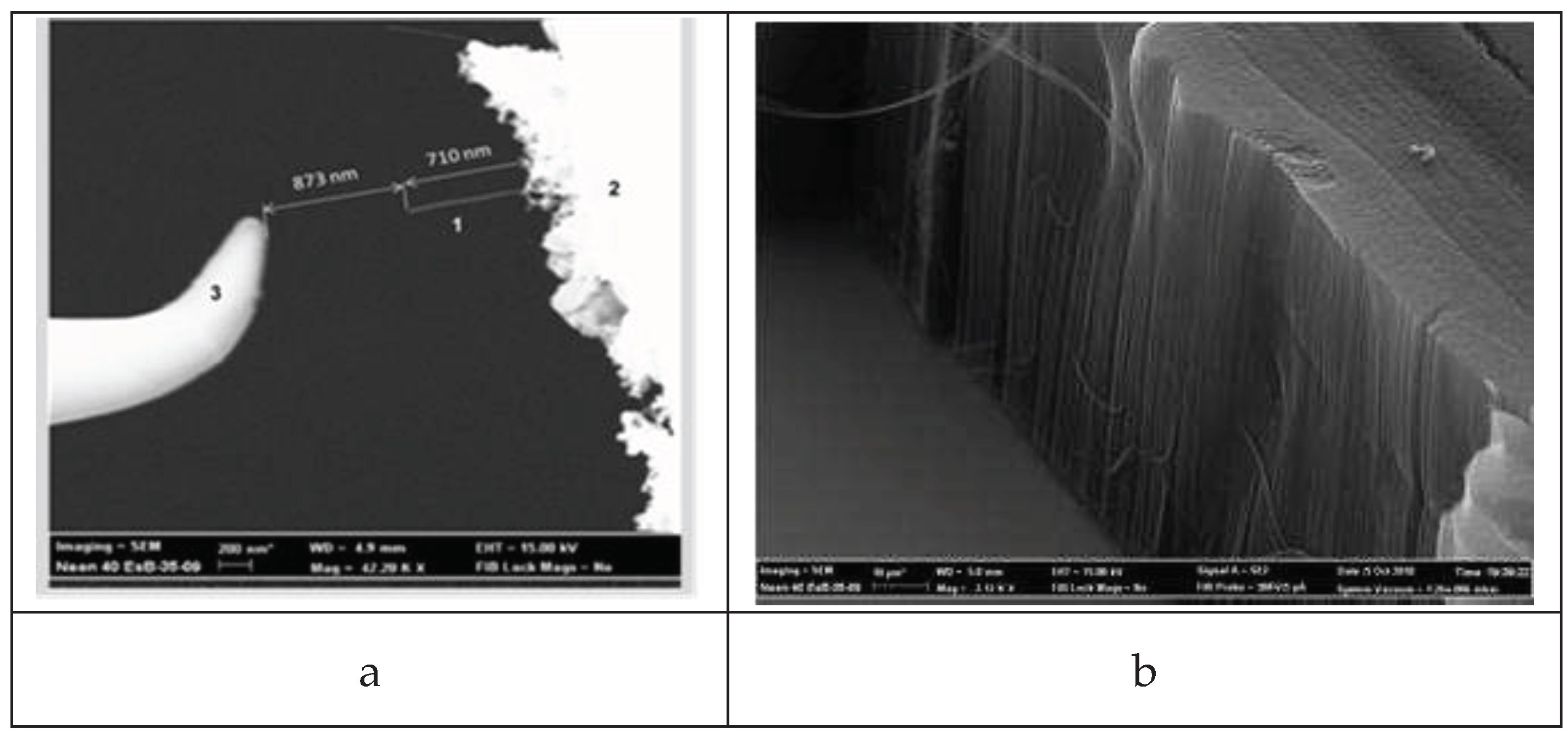
Figure 1. The samples of CNTs studied in SEM. (a) SEM image of the single CNT in the scheme for measuring its current-voltage characteristic (I–V) characteristics on a nanodiode mock-up. 1 - nanotube emitter, 2- cathode, 3 tungsten microwire anode. The CNT length is 710 nm, the distance to the anode is 873 nm. (b) The array of the oriented CNTs.
Preprints 80766 g001
Figure 2. Scheme of measurements of the I-V characteristics of nanodiode samples based on CNTs in the SEM chamber.
Preprints 80766 g002
Figure 3. Micrographs of CNT samples obtained in different microscopes. (a) SEM image of CNTs with different types of large-scale lattice deformations, defined with the letters “a”,”b”,”c”,”d” on the figure.
Preprints 80766 g003
Figure 4. AFM image of CNT superlattices, at E=0, Ug=0, the inset shows the scheme of voltage application to CNT.
Preprints 80766 g004
Figure 5. Study of superlattices detected in single CNTs in SEM, AFM and STM. (a) Superlattice revealed in SEM image, period about 30-40 nm. The emission current flows along the CNT. (b) AFM image of a CNT superlattice (period ~30–40 nm). The emission current flows along the CNT. (c) STM micrograph of a superlattice in CNTs (period ~3 nm). The applied electric field is perpendicular to the CNT axis.
Preprints 80766 g005
Figure 6. SEM image of a nanodiode in secondary electrons.
Preprints 80766 g006
Figure 7. SEM micrograph showing a diode structure, one of the electrodes of which is a single CNT deposited on a tungsten electrode.
Preprints 80766 g007
Figure 8. I–V characteristic of the field emission measured on the nanodiode model (a) and the corresponding graph plotted in log(I/U2)-1/U coordinates (b). The dotted line is a straight line corresponding to the Fowler-Nordheim function.
Preprints 80766 g008
Disclaimer/Publisher’s Note: The statements, opinions and data contained in all publications are solely those of the individual author(s) and contributor(s) and not of MDPI and/or the editor(s). MDPI and/or the editor(s) disclaim responsibility for any injury to people or property resulting from any ideas, methods, instructions or products referred to in the content.
Copyright: This open access article is published under a Creative Commons CC BY 4.0 license, which permit the free download, distribution, and reuse, provided that the author and preprint are cited in any reuse.
Prerpints.org logo

Preprints.org is a free preprint server supported by MDPI in Basel, Switzerland.

Subscribe

© 2024 MDPI (Basel, Switzerland) unless otherwise stated