
Submitted:
12 July 2023
Posted:
13 July 2023
You are already at the latest version
Abstract
In this study we assessed the electrical and optical behavior of semiconductor hybrid films fabricate from octaethyl-21H,23H-porphine copper (CuP), embedded in polymethylmethacrylate (PMMA), and polystyrene (PS). The hybrid films were characterized structurally and morphologically by means of Infrared spectroscopy (IR), atomic force microscopy (AFM), scanning electron microscopy (SEM) and X-ray diffraction (XRD). Subsequently, the PMMA:CuP and PS:CuP hybrid films were evaluated optically by UV-vis spectroscopy, as well as electrically, with the four-point collinear method. Hybrid films present a homogeneous and low roughness morphology, besides; the PS matrix allows the crystallization of the porphin, while the PMMA promotes the amorphous structure in CuP. The polymeric matrix also has an effect on the optical behavior of the films, since the smallest optical gap (2.16 eV) and onset gap (1.89 eV) and the highest transparency are obtained in the film with a PMMA matrix. Finally, the electrical behavior in hybrid films is also affected by the matrix: the largest amount of current carried is around 0.01 A for PS:CuP film, while for PMMA:CuP film it is 0.0015 A. Thanks to the above properties, hybrid films are promising candidates for use in optoelectronic devices.
Keywords:
Polymeric Matrix
; Porphine
; Hybrid Film
; Optical Properties
; Electrical Behavior
1. Introduction
Organic semiconductors are structures that contain several carbon-carbon bonds and are able to carry out electronic conduction as inorganic semiconductors [1]. This type of semiconductor has different features such as low weight, transparency, higher brightness, flexibility, easy to process, and can be used to fabricate inexpensive devices [2,3,4,5]. Some applications for these materials are electronic paper, supercapacitors, organic light-emitting diodes (OLEDs), thin film batteries, organic photovoltaics, organic field-effect transistors, solar cells, sensors, and biosensors [2,3,4,5,6]. Organic semiconductors can be divided into two main groups, small molecule materials and conductive polymers. From a chemical point of view, there are significant differences between the categories, which directly affect its performance in technology. Small molecule materials, also known as molecular materials, are classified into two categories, pigments (insoluble in organic solvents) and dyes (soluble in organic solvents). Polymeric macromolecules are soluble in organic solvents and are formed through the repetition of a main unit, which is the monomer. In addition, polymers can be solution processed because of their chemical properties, in contrast to small molecule materials that must be thermally evaporated [2].
Porphines belong to the small molecule group and are identified as the core macrocycle of synthetic and natural porphyrins, also it is known as the simplest porphyrin [7]. It has a large π-conjugated system, high thermal stability, good photosensitizing ability, [8] and high molar absorptivity at the Soret peak [9]. The use of porphines have some challenges including that they are unfeasible to synthesize on a large scale and high insolubility [7]. To find an answer to the solubility problem, porphines can be processed in the solid state. In organic electronics, porphyrin chemistry represents an extensive area of interest and has already reached the stage of advanced applications, where films of these materials are investigated for their use as chemical sensors for volatile organic compounds, information storage and non-linear optical materials [10]. A starting point for the fabrication of highly functional thin films is the monolayer and multilayer formation. The use of covalently bound self-assembly is an important advantage because the weak van der Waals interactions or hydrogen bonding between interfaces are replaced with covalent bonds. One of the porphyrins that is considered as the most helpful and has been utilized in the development of thin films is the manganese(III) porphyrin. Susuki et al. accounted the manganese porphyrin as an active material [11], and Khorasani et al. as ionophores in thiocyanate-selective sensors [12]. Even so, the best result reported for film sensor was obtained with tetratolylporphine manganese (III) chloride (MnTTPCI); it has steady and reproducible electrochromic properties, and possesses properties that serve to function as a detecting material for optical gas [13].
Functionalized porphyrins can be used in thin films like sensitizers, in their free-base form or with a redox inactive metal such as zinc inside the macrocycle cavity. The above because the porphyrins reveal strong light absorption with a Soret band in the 400-450 nm range and visible bands in the 500-650 nm range [14]. Thanks to this optical property, the highest efficiency organic solar cell reported is specifically composed of Co(II/III)tris(bipyridyl)–based redox electrolyte and a custom synthesized donor-π-bridge-acceptor zinc porphyrin dye as sensitizer (YD2-o-C8), the performance of the device can reach an efficiency of 12.3% under simulated air mass 1.5 global sunlight. The YD2-o-C8 molecule retards the rate of interfacial back electron transfer from the conduction band of the nanocrystalline titanium dioxide film to the oxidized cobalt mediator, which enables it to reach 1 volt. In addition, the YD2-o-C8 porphyrin generates large photocurrents because it collects the sunlight across the visible spectrum [15]. Nevertheless, one disadvantage of YD2-o-C8 is that in the region 500-600 nm and in the long wavelength region, it shows very low molar extinction coefficients, which decreases the light collecting properties. Considerable effort has been put into solving this problem, but it has not been completely resolved [16]. The use of films composed of porphine with some conductive polymer may be a feasible option, conducting polymers are the second type of organic semiconductors, and recently, they are being investigated in areas such as bioelectronics, bio-interfaces and medical aspects [17,18]. Polymethylmethacrylate (PMMA) and polystyrene (PS) are part of the category of polymers used in molecular electronics. PMMA, as a polymeric waveguide has been highlighted for use in optoelectronic devices and as optical components because of its volume productivity and low cost [19]. Some examples of optical components are transceiver, optical switch, splitter, and coupler [19]. In the case of PS it is considered one of the oldest commercial polymers. Some features that stand out of this polymer are its crystal-clear appearance, affordability, aromatics, its amorphous structure, stiffness, hardness and processability. However, both polymers are also brittle materials, have poor chemical resistance, low melting point, and low flexibility. To solve the issues mentioned above, its properties can be modified [19,20]. These modifications include forming hybrid films with the polymer and some small molecules with semiconductor behavior.
Based on the above, this study proposes (i) the manufacture of semiconductor hybrid films using copper porphine (CuP) as a small molecule in addition to PMMA and PS as matrix, (ii) the structural and surface topographic characterization of hybrid films and (iii) the evaluation of their optical and electrical properties. The novelty of this work is related to the development of new hybrid films polymer-CuP that can be used in an emerging category of optoelectronic devices. In addition to the comparative study between PMMA and PS matrices
2. Materials and Methods
Poly(methyl methacrylate) (PMMA; [CH2C(CH3)(CO2CH3)]n), polystyrene (PS; [CH2CH(C6H5)]n), and 2,3,7,8,12,13,17,18-Octaethyl-21H,23H-porphine copper(II) (CuP; C36H44CuN4) were obtained from commercial suppliers (Sigma-Aldrich, Saint Louis, MO, USA) and used without further purification. The hybrid films were deposited on Corning glass, n-type silicon and fluorine doped tin oxide coated glass slide (FTO). It is important to emphasize that the glass and FTO substrates were previously washed in an ultrasonic bath with dichloromethane, methanol, and acetone. The n-silicon was washed with a “p” solution (10 ml HF, 15 ml HNO3, and 300 ml H2O). The hybrid films were fabricated from a dispersion with 6 mL of the polymer and CuP from a dilution of 10 wt% in toluene for PS and acetone for PMMA. The mixture was dispersed using the G560 shaker of Scientific Industries Vortex-Genie (Bohemia, NY, USA). A syringe was used to apply 0.6 mL on the surface and then spread the dispersion. Directly after spreading the dispersion, the films were brought to 55°C for 5 minutes in the drying oven Briteg SC-92898 (Instrumentos Científicos, S.A de C.V.). This accelerated the hybrid film fabrication process and prevented the samples from swelling and cracking during drying. The n-silicon substrates were used for infrared (IR) spectroscopy evaluation using the Nicolet iS5-FT spectrometer (Thermo Fisher Scientific Inc., Waltham, MA, USA) at a wavelength range of 4000 to 400 cm-1. Topographical characteristics were investigated with a Nano AFM atomic force microscope (AFM, Nanosurf AG, Liesta, Switzerland) using an Ntegra platform. For the morphological characterization of the film on glass, a Hitachi Tabletop Microscope TM3030 (Hitachi High-Tech, HITACHI, Toyo, Japan) was used at 5 kV. The hybrid films on glass were subjected to X-ray diffraction analysis using the θ–2θ technique, in a Rigaku Miniflex 600 diffractometer (Rigau Corporation, Tokyo, Japan), Cu Kα (λ=1.5406 Å), at 40 kV, 20 mA. The absorbance and transmittance were obtained with the glass substrate, in order to get the optical band gap, using an Ultraviolet-visible (UV-Vis) spectrophotometer 300 Unicam (Thermo Fisher Scientific Inc., Waltham, MA, USA), in a wavelength range from 200 to 1100 nm. In order to evaluate the effect of the radiation on the band gap of hybrid films, an irradiation of 360 watts, 82V Bias Dukane 28A653A lamp was used for 3 hours. Followed the accelerated radiation test, the UV-vis spectroscopy in films were evaluated again. The FTO substrates were used for measuring the current-voltage (I-V) characteristics. A Keithley 4200-SCS-PK1 auto-ranging picoammeter (Tektronix Inc., Beaverton, OR, USA) was used with the collinear four-point probe method, in a sensing station with lighting and temperature controller circuits from Next Robotix (Comercializadora K Mox, S.A. de C.V., Mexico City, Mexico). The samples were illuminated with commercial LEDs of wavelengths between 400 and 700 nm (from red color to near-ultraviolet), using a lighting controller circuit from Next Robotix. For these LEDs, typical operating voltages varied between 1.8 and 2.8 V, with a typical operating current of 18 mA.
3. Results and Discussion
3.1. Structural and Morphological Characterization of Hybrid Films
The IR spectroscopy was performed with the purpose to identify their main bonds and chemical stability of CuP and polymers after the deposit of the hybrid films. FTIR spectra of films are illustrated in Figure 1, the observed IR bands and their assignments are recorded in Table 1, which are in a good agreement with the literature [13,20,21,22,23,24,25,26,27]. The presence of C–H groups was indicated by the bands at 2845 cm-1 (CH3 asymmetric stretching), at 2925±3 cm-1 (symmetrical CH2), and 1441±4, 1379±7, 703±1 cm-1 (asymmetrical CH2) [28,29,30,31], whereas the presence of C-C was indicated by the band at 1462±2 cm-1 [13,20,21,22,23,24,25,26,27,31]. Additionally, the presence of a pyrrole C-N bond was indicated by the band at 1021±2 cm-1 [13,20,21,22,23,24,25,26,27,31], and the bands at 1066 and 844±2 cm-1 are related to N-H vibration [13,20,21,22,23,24,25,26,27,28,29,30]. On the other hand, the presence of PMMA in the PMMA:CuP film is verified by the signals at 1739, 1634 and 1134 cm-1 and the PS signals in the PS:CuP film are found at 3026, 2922, 1606 and 757 cm-1, and are shown with their respective assignments in Table 1. Accordingly, the presence of all these bands confirms the incorporation of CuP in the polymeric matrix and, in addition, this also suggests that the CuP is structurally unchanged during the preparation of hybrid films. However, it is necessary to analyze their topography, to determine if the CuP was adequately distributed in the polymeric matrix.
In order to know the surface topography and roughness of the PMMA-CuP and PS:CuP films, they were analyzed by AFM and Figure 2 shows the images at 5x5 μm. The hybrid films show a very uniform topography with some ridges, probably related to preferential directions of growth. However, in both films it would appear that the porphin is completely embedded in the polymeric matrix. Regarding the Root Mean Square roughness, the film with PMMA is less rough than the film with the PS matrix, the values obtained are 2.59 and 3.66 nm respectively. The low roughness and adequate homogeneity of hybrid films makes them susceptible to being used as components in optoelectronic devices, however; it is necessary to complement the morphological characterization by SEM.
In order to complement the surface morphology of the PMMA-CuP and PS:CuP films, they were analyzed by SEM and Figure 3 shows the images at 800x. It can be observed that both images exhibit the same continuous and homogenous surface, with minor imperfections due to the manufacturing process. This implies that in both films, the CuP is homogeneously distributed within the polymeric matrix.
The structure of the hybrid films was studied by X-ray diffraction and the diffraction patterns are given in Figure 4. In the PMMA:CuP film, the XRD pattern exhibits a broad diffused peak around 17°- 34° without detectable sharp Bragg peaks that can be related to a crystalline phase. This implies that the film is essentially amorphous and the porphine has poor crystallinity in the film [32]. The PS:CuP film, besides the broad diffused peak around 14°-35°, presents a sharp Bragg peaks around 2θ = 7.11°, 7.89°, 19° indicate some degree of π-π stacking of the CuP molecules in certain regions of the hybrid film, which suggest that the PS:CuP film have a crystalline structure [32]. Apparently, there is a small nucleation and crystallization of the CuP with a preferential direction of growth [32,33,34]. The greater crystallinity in the PS:CuP hybrid film could be reflected in better optical and electrical properties, however, it is important to consider that the porphine is embedded in a polymeric matrix, therefore the predominant structure of the hybrid film is amorphous.
3.2. Evaluation of Optical Parameters in Hybrid Films
In order to study the optical properties of the PMMA:CuP and PS:CuP films, UV-vis spectroscopy was carried out, and it is important to consider that these spectra are dominated by porphine π-π* transitions. The spectral distribution of transmittance (%T) and absorbance (A) as a function of the wavelength for the polymer:CuP films are shown in Figure 5. In Figure 5a it is shown that at longer wavelength greater than 650 nm, the hybrid films become nearly transparent as there is no light being absorbed, while in the ultraviolet range, sharp band edge absorption is observed for the two films. The presence of such edges in these films makes them potential candidates for optical filter components. Although the transmittance obtained in the hybrid films reaches a maximum of 68% for PS:CuP and 84% for PMMA:CuP, this value is lower than that reported in the literature for other metallic porphine films, such as porphine iron (III) chloride (FeTPPCl) [10], manganese (III) chloride tetraphenyl porphine (MnTPPCl) [13], for platinum octaethylporphyrin PtOEP [33], and for cobalt porphine CoMTTPP [35] presenting %T > 90%. However, the spectral distribution of transmittance is similar to the previous examples and above all, the PS:CuP film could be used (at wavelengths greater than 650 nm), as a transparent anode in photovoltaic devices.
With respect to the absorbance presented in Figure 5b, the spectra of PS:CuP show three bands: an intense band at 401 nm (Soret-band) and a doublet at 526 nm (β-band) and 562 nm (∝-band) that is related to Q-bands. For PMMA:CuP the spectra shown the three bands at 398 (Soret-band), 539 (β-band) and 586 nm (∝-band). The peaks of Soret and Q-bands are interpreted as the excitation between bonding and antibonding molecular orbital in the porphine, in terms of π-π* [13] and the results obtained for the PMMA:CuP and PS:CuP films coincide with those obtained for other structures with porphines [7,34]. The absorption capacity of the CuP makes hybrid films susceptible to participate in photoinduced charge transfer processes in optoelectronic and photovoltaic devices.
In organic semiconductors it is usual to study the type of optical transitions in the material, as well as their value of the optical band gap. The transitions in the CuP are promoted from the valence band “π-band” to the conduction band “π*-band”, and these orbitals are separated by the band gap. There is an expression that relates the absorption coefficient (α):
to the optical band gap (Egopt), and it is the Tauc’s relation [36,37,38]:
where T is the transmittance, d is the thickness of the film (12 μm for PMMA:CuP and 78 μm for PS:CuP), h is the Planck constant, ν is the frequency obtained from ν = c/λ, λ is the wavelength, c is the speed of light, G is a parameter that depends on the transition probability, and r is a number which characterizes the type of electronic transitions, and where r=2 for indirect allowed transitions, corresponding to semiconductors films with a mainly amorphous structure. Moreover, the indirect allowed transition was observed in several metalloporphines such as iron [10], manganese [13], platinum [33], cobalt [35], and nickel [39]. The indirect band gap for PMMA:CuP and PS:CuP films are evaluated by extrapolating the linear portion of the plot to (αhν)1/2= 0. The obtained values are shown in Figure 6a,b, the first energy value is the onset band gap, Egonset (1.89 and 2.07 eV for PMMA:CuP and PS:CuP respectively) and corresponds to the formation of a bound electron-hole pair, or onset band gap [33,40]. The second energy (2.16 and 2.86 eV for PMMA:CuP and PS:CuP respectively) is the optical band gap, Egopt, and corresponds to the energy gap between the valence band and the conduction band [10,40]. These results are important not only because they are in the same order of magnitude as those obtained for other porphine and their derivatives [33,34,35,36,37,38,39], but also because the PMMA or PS polymeric matrix does not increase the porphine band gap in hybrid films. One of the drawbacks in hybrid films, due to the presence of the polymeric matrix, is that it can reduce charge transport due to the interfaces that occur between the polymer and the porphine. In this case, Egopt and the Egonset are not affected, although surely in the films there are a significant number of traps and defects that can be indirectly evaluated through the Urbach energy (EU). The EU corresponds to the width of the band tail, which is related to localized states within the energy gap, possibly caused by structural defects [41]. The EU can be used to determine the defects in the bandgap and can be determined according to the expression [41]:
α=ln(T/d)
(αhν)r = G(hν – Egopt),
In addition to the parameters defined above, Aa is a constant of the material that conforms to α at the energy gap. The values of the EU were determined from the reciprocal of the slope from this linear relation and have been recorded in Figure 6c,d. It is important to consider that the value of EU is zero in a perfect semiconductor [42] and in this study EU of 0.70 and 0.25 eV have been obtained for PMMA:CuP and PS:CuP films respectively. The above results are indicative of the higher number of defects and traps in the film with the PMMA matrix, which is evident from the amorphous structure of PMMA:CuP shown in Figure 4. On the other hand, It is remarkable how the film with the PS matrix presents a lower EU than that obtained even in pristine porphine films such as the MnTPPCl one obtained by Alharbi et al. [13]. Apparently, the higher degree of porphine crystallinity observed on the XRD and presented in Figure 4, is responsible for the low EU; however, the matrix also has an effect on the optical behavior of the films, since the smallest optical and onset band gaps and the highest transparency are obtained in the film with a PMMA matrix with respect to the PS matrix.
3.3. Evaluation of Electrical Behavior
To evaluate the electrical properties of the PMMA:CuP and PS:CuP films, the I-V characteristic curves were obtained for glass/FTO/PMMA:CuP/Ag and glass/FTO/PS:CuP/Ag simple devices under different incident light colors. It can be observed in Figure 7a, a change in the curve behavior for the natural light conditions of the glass/FTO/PMMA:CuP/Ag device. The rest of the curves for this device present the same behavior: the change in the type of radiation that falls on it does not affect the amount of current that flows through the device. At V < 0.8 V the behavior is mainly ohmic and at V > 0.8V there is a decrease in the amount of current carried, probably due to charge saturation at the polymer-CuP interfaces. As the voltage increases and with it, the concentration of charges in certain areas of the amorphous film, the flow of current becomes more difficult, however, at around 1V, the charges flow again and the device continues with ohmic behavior. It is interesting to observe in Figure 7a, how this saturation of charge carriers does not occur when changing the direction of the flow, reversing the anode and cathode. In this inverse sense, the electrical behavior remains ohmic throughout the analyzed voltage range, so it can be deduced that for the device with the PMMA:CuP film, the type of material that acts as electrode is important, as well as the direction of flow of charges. Figure 7c shows the curves with the variation of the current density (J) with respect to the applied voltage, obtained for conditions of natural lighting and darkness. In these two curves, the difference in the flow of transported charge becomes evident: in the device under dark conditions, the J is an order of magnitude higher than in daylight conditions, suggesting that PMMA:CuP film can have photovoltaic properties and be used in the manufacturing of solar cells or photodiodes. However, it is possible to observe that the J in natural lighting conditions presents an ohmic behavior at V < 1.1V and a Space Charge-Limited Current (SCLC) behavior at V > 1.1V. This last mechanism is generated because, as previously mentioned, by increasing the voltage, a situation is reached in which the charge carriers do not move fast enough and accumulate in certain regions of the film. Under these conditions, the film is no longer homogeneous and the device enters the SCLC regime. The behavior of the glass/FTO/PMMA:CuP/Ag device shown in Figure 7c, under natural lighting conditions, is that of a resistor. Apparently the weak intra- and intermolecular interactions in the PMMA:CuP amorphous film hinder the flow of charge carriers.
On the other hand, the glass/FTO/PS:CuP/Ag device (Figure 7b) presents a similar behavior in all lighting conditions to which it was subjected, and the current it carries is an order of magnitude greater than in the device with PMMA matrix. Furthermore, its behavior is not ambipolar either and is more related to that of a Schottky diode, with an exponential relationship between the applied voltage and the amount of electric current carried. In the curves of Figure 7b, a slight change in the slope of the curves is observed around 0.9 V, although it is minimal, and based on the electrical behavior, it could be concluded that the PS:CuP film presents a greater potential to be used as a component in optoelectronic devices with respect to the PMMA:CuP film. The greater order in the structure of this hybrid film offers less difficulty for the charge transporters to move through the energy bands and their mobility is greater. Finally, it is important to observe how the polymer used as matrix exerts a marked influence on the optical and electrical properties of porphine films. While the PMMA matrix favors the transparency of the film and the low band gap values, the PS matrix increases the charge flow along the hybrid film and changes the behavior of the resistor generated by the PMMA matrix, to a Schottky diode type device. However, the hybrid films are promising candidates for use as active layer in optoelectronic and photovoltaic devices.
4. Conclusions
Using a simple dispersion-polymerization technique, hybrid films were fabricated with copper porphine embedded in PMMA and PS polymeric matrices. The films were characterized structurally by IR and DRX and morphologically by AFM and SEM. The DRX analysis showed that the PMMA:CuP film is mainly amorphous and the PS:CuP has a crystalline structure. Although the optical properties of the films are dominated by the presence of CuP, the polymer used as matrix can significantly modify them. The PMMA:CuP film has an optical band gap of 2.16 eV and a onset gap of 1.89 eV and the PS film has an optical band gap and onset gap of 2.86 eV and 2.07 eV respectively. The electrical behavior in films is also affected by the type of polymer: the largest amount of current carried is around 0.01 A for PS:CuP film, while for PMMA:CuP film it is 0.0015 A. Furthermore, the behavior of the device with this hybrid film is similar to that of a resistor, while the device with the PS:CuP film is more similar to that of a Schottky diode. However, thanks to the above properties, hybrid films are promising candidates for use as an active layer in optoelectronic and photovoltaic devices.
Author Contributions
Conceptualization, M.E.S.V. and J.A.H.M.; methodology, J.A.H.M., D.G.V. and I.M.G.F.; software, M.E.S.V. and J.A.H.M.; validation, M.E.S.V., I.M.G.F. and O.L.F.; formal analysis, M.E.S.V. and O.L.F.; investigation, J.A.H.M., D.G.V. and O.L.F.; resources, M.E.S.V. and O.L.F.; data curation, M.E.S.V., J.A.H.M., D.G.V. and O.L.F.; writing—original draft preparation, M.E.S.V., J.A.H.M., D.G.V., I.M.G.F. and O.L.F.; writing—review and editing, M.E.S.V., D.G.V., I.M.G.F. and O.L.F.; visualization, M.E.S.V. and J.A.H.M.; supervision, M.E.S.V.; project administration, M.E.S.V. and O.L.F.; funding acquisition, M.E.S.V. and O.L.F. All authors have read and agreed to the published version of the manuscript.
Funding
María Elena Sánchez-Vergara acknowledge the financial support from Anahuac México University, Project number PI0000067.
Conflicts of Interest
The authors declare no conflict of interest.
References
- Juster, N.J. Organic semiconductors. J. Chem. Educ. 1963, 40, 547–552. [Google Scholar] [CrossRef]
- Martín-Palma, R.J.; Martínez-Duart, J.M. Novel Advanced Nanomaterials and Devices for Nanoelectronics and Photonics. Nanophotonics 2017, 1, 243–263. [Google Scholar] [CrossRef]
- Bronstein, H.; Nielsen, C.B.; Schroeder, B.C; McCulloch, I. The role of chemical design in the performance of organic semiconductors. Nat. Rev. Chem. 2020, 4, 66–77. [Google Scholar] [CrossRef] [PubMed]
- Chen, F.C. Organic Semiconductors. J. Mod. Opt. 2018, 5, 220–231. [Google Scholar] [CrossRef]
- Khambhati, D.P.; Nelson, T.L. Semiconductive materials for organic electronics and bioelectronics from renewable resources. In Sustainable Strategies in Organic Electronics, 1st ed.; Marrocchi, A., Ed.; Publisher: Woodhead Publishing, United Kingdom, 2022; Volume 1, pp. 209–227. [Google Scholar] [CrossRef]
- Scheunemann, D.; Kemerink, M. Thermoelectric properties of doped organic semiconductors. In Organic Flexible Electronics, 1st ed.; Cosseddu, P., Caironi, M., Eds.; Publisher: Woodhead Publishing, United Kingdom, 2020; Volume 1, pp. 165–197. [Google Scholar] [CrossRef]
- Senge, M.O.; Davis, M. Porphyrin (porphine) – A neglected parent compound with potential. J. Porphyr. Phthalocyanines 2010, 14, 557–567. [Google Scholar] [CrossRef]
- Bera, R.; Jana, B.; Mondal, B.; Patra, A. Design of CdTeSe – Porphyrin – Graphene Composite for photoinduced Electron Transfer and Photocurrent Generation. ACS Sustainable Chem. Eng. 2017, 5, 3002–3010. [Google Scholar] [CrossRef]
- Palomaki, P.K.B.; Civic, M.R.; Dinolfo, P.H. Photocurrent Enhancement by Multilayered Porphyrin Sensitizers in a Photoelectrochemical Cell. ACS Appl. Mater. Interfaces 2013, 5, 7604–7612. [Google Scholar] [CrossRef]
- El-Nahass, M.M.; El-Deeb, A.F.; Metwally, H.S.; Hassanien, A.M. Influence of annealing on the optical properties of 5,10,15,20-tetraphenyl-21H, 23H-porphine iron (III) chloride thin films. Mater. Chem. Phys. 2011, 125, 247–251. [Google Scholar] [CrossRef]
- Suzuki, H.; Nakagawa, H.; Mifune, M.; Saito, Y. Triiodide Ion-Selective Electrode Based on Manganese(III)-Tetraphenylporphine. Anal. Sci. 1993, 9, 351–354. [Google Scholar] [CrossRef]
- Khorasani, J.H.; Amini, M.K.; Motaghi, H.; Tangestaninejad, S.; Moghadam, M. Manganese porphyrin derivatives as ionophores for thiocyanate-selective electrodes; the influence of porphyrin substituents and additives on the response properties. Sens. Actuators B Chem 2002, 87, 448–456. [Google Scholar] [CrossRef]
- Alharbi, S.R.; Darwish, A.A.A.; Garni, S.E.A.; ElSaeedy, H.I.; El-Rahman, K.F.A. Influence of thickness and annealing on linear and nonlinear optical properties of manganese (III) chloride tetraphenyl porphine (MnTPPCl) organic thin films. Infrared Phys. Technol. 2016, 78, 77–83. [Google Scholar] [CrossRef]
- Hart, A.S.; KC, C.B.; Gobeze, H.B.; Sequeira, L.R.; D’Souza, F. Porphyrin-Sensitized Solar Cells: Effect of Carboxyl Anchor Group Orientation on the Cell Performance. ACS Appl. Mater. Interfaces 2013, 5, 5314–5323. [Google Scholar] [CrossRef] [PubMed]
- Yella, A.; Lee, H.; Tsao, H.N.; Yi, C.; Chandiran, A.K.; Nazeeruddin, M.K.; Diau, E.W.; Yeh, C.; Zakeeruddin, S.M.; Gratzel, M. Porphyrin-sensitized solar cells with cobalt (II/III)-based redox electrolyte exceed 12 percent efficiency. Science 2011, 334, 629–634. [Google Scholar] [CrossRef] [PubMed]
- Karthikeyan, S.; Lee, J.Y. Zinc-Porphyrin Based Dyes for Dye-Sensitized Solar Cells. J. Phys. Chem. A 2013, 117, 10973–10979. [Google Scholar] [CrossRef]
- Bhat, M.A.; Rather, R.A.; Shalla, A.H. PEDOT and PEDOT:PSS conducting polymeric hydrogels: A report on their emerging applications. Synth. Met. 2021, 273, 116709. [Google Scholar] [CrossRef]
- Zhang, B.; Sun, J.; Katz, H.E.; Fang, F.; Opila, R.L. Promising Thermoelectric Properties of Commercial PEDOT:PSS Materials and Their Bi2Te3 Powder Composites. ACS Appl. Mater. Interfaces 2010, 2, 3170–3178. [Google Scholar] [CrossRef]
- Zidan, H.M.; Abu-Elnader, M. Structural and optical properties of pure PMMA and metal chloride-doped PMMA films. Phys. B: Condens. Matter 2005, 355, 308–317. [Google Scholar] [CrossRef]
- Vodnik, V.V.; Dzunuzovic, E.S.; Dzunuzovic, J.V. Synthesis and Characterization of Polystyrene Based Nanocomposites. In Polystyrene: Synthesis, characteristics and applications, 1st ed.; Lynwood, C., Ed.; Publisher: Nova Science Publishers, United States, 2014; Volume 1, pp. 201–240. [Google Scholar]
- Al-Muntaser, A.A.; El-Nahass, M.M.; Oraby, A.H.; Meikhail, M.S.; Zeyada, H.M. Structural and optical characterization of thermally evaporated nanocrystalline 5,10,15,20-tetraphenyl-21H,23H-porphine manganese (III) chloride thin films. Optik 2018, 167, 204–217. [Google Scholar] [CrossRef]
- Li, X.Y.; Zgierski, M.Z. Porphine force field: in-plane normal modes of free-base porphine; comparison with metalloporphines and structural implications. J. Phys. Chem. 1991, 95, 4268–4287. [Google Scholar] [CrossRef]
- Cristescu, R.; Popescu, C.; Popescu, A.C.; Grigorescu, S.; Mihailescu, I.N.; Ciucu, A.A.; Iordache, S.; Andronie, A.; Stamatin, I.; Fagadar-Cosma, E.; Chrisey, D.B. MAPLE deposition of Mn (III) metalloporphyrin thin films: structural, topographical and electrochemical investigations. Appl. Surf. Sci. 2011, 257, 5293–5297. [Google Scholar] [CrossRef]
- Fagadar-Cosma, E.; Mirica, M.C.; Balcu, I.; Bucovicean, C.; Cretu, C.; Armeanu, I.; Fagadar-Cosma, G. Syntheses, spectroscopic and AFM characterization of some manganese porphyrins and their hybrid silica nanomaterials. Molecules 2009, 14, 1370–1388. [Google Scholar] [CrossRef] [PubMed]
- Saeedi, M.S.; Tangestaninejad, S.; Moghadam, M.; Mirkhani, V.; Mohammadpoor-Baltork, I.; Khosropour, A.R. Manganese porphyrin immobilized on magnetite nanoparticles as a recoverable nanocatalyst for epoxidation of olefins. Mater. Chem. Phys. 2014, 146, 113–120. [Google Scholar] [CrossRef]
- Tommasini, F.J.; Ferreira, L.C.; Pimenta-Tienne, L.G.; Aguiar, V.O.; Prado-Silva, M.H.; Mota-Rocha, L.F.; Vieira-Marques, M.F. Poly (Methyl Methacrylate)-SiC Nanocomposites Prepared Through in Situ Polymerization. Mater. Res. 2018, 21, 86. [Google Scholar] [CrossRef]
- Mehdinia, A.; Salamat, M.; Jabbari, A. Preparation of a magnetic polystyrene nanocomposite for dispersive solid-phase extraction of copper ions in environmental samples. Sci. Rep. 2020, 10, 3279. [Google Scholar] [CrossRef]
- Fagadar-Cosma, E.; Enache, C.; Vlascici, D.; Fagadar-Cosma, G.; Vasile, M.; Bazylake, G. Novel nanomaterials based on 5,10,15,20-tetrakis(3,4-dimethoxyphenyl)-21H,23H-porphyrin entrapped in silica matrices. Mat. Res. Bull. 2009, 44, 2186–2193. [Google Scholar] [CrossRef]
- Tazeev, D.; Musin, L.; Mironov, N.; Milordov, D.; Tazeeva, E.; Yakubova, S.; Yakubov, M. Complexes of Transition Metals with Petroleum Porphyrin Ligands: Preparation and Evaluation of Catalytic Ability. Catalysts 2021, 11, 1506. [Google Scholar] [CrossRef]
- Thomas, D.W.; Martell, A.E. Metal Chelates of Tetraphenylporphine and of Some p-Substituted Derivatives. J. Am. Chem. Soc. 1959, 81, 5111–5119. [Google Scholar] [CrossRef]
- Kumolo, S.T.; Yulizar, Y.; Haerudin, H.; Kurniawaty, I.; Apriandanu, D.O.B. Identification of metal porphyrins in Duri crude oil. IOP Conf. Ser.: Mater. Sci. Eng. 2019, 496, 012038. [Google Scholar] [CrossRef]
- Novoa-Cid, M.; Melillo, A.; Ferrer, B.; Alvaro, M.; Baldovi, H.G. Photocatalytic Water Splitting Promoted by 2D and 3D Porphyrin Covalent Organic Polymers Synthesized by Suzuki-Miyaura Carbon-Carbon Coupling. Nanomaterials 2022, 12, 3197. [Google Scholar] [CrossRef]
- Abuelwafa, A.A.; El-Denglawey, A.; Dongol, M.; El-Nahass, M.M.; Soga, T. Influence of annealing temperature on structural and optical properties of nanocrystalline Platinum octaethylporphyrin (PtOEP) thin films. Opt. Mater. 2015, 49, 271–278. [Google Scholar] [CrossRef]
- Myltykbayeva, Z.K.; Seysembekova, A.; Moreno, B.M.; Sánchez-Tovar, R.; Fernández-Domene, R.M.; Vidal-Moya, A.; Solsona, B.; López-Nieto, J.M. V-Porphyrins Encapsulated or Supported on Siliceous Materials: Synthesis, Characterization, and Photoelectrochemical Properties. Materials 2022, 15, 7473. [Google Scholar] [CrossRef] [PubMed]
- El-Nahass, M.M.; Ammar, A.H.; Farag, A.A.M.; Atta, A.A.; El-Zaidia, E.F.M. Effect of heat treatment on morphological, structural and optical properties of CoMTPP thin films. Solid State Sci. 2011, 13, 596–600. [Google Scholar] [CrossRef]
- Tauc, J. Optical Properties and Electronic Structure of Amorphous Ge and Si. Mater. Res. Bull. 1968, 3, 37–46. [Google Scholar] [CrossRef]
- Laidani, N.; Bartali, R.; Gottardi, G.; Anderle, M.; Cheyssac, P. Optical Absorption Parameters of Amorphous Carbon Films from Forouhi–Bloomer and Tauc–Lorentz Models: A Comparative Study. J. Condens. Matter Phys. 2007, 20, 015216. [Google Scholar] [CrossRef]
- Mok, T. M.; O’Leary, S. K. The Dependence of The Tauc and Cody Optical Gaps Associated with Hydrogenated Amorphous Silicon on the Film Thickness: Al Experimental Limitations and The Impact Of Curvature In The Tauc And Cody Plots. J. Appl. Phys. 2007, 102, 113525. [Google Scholar] [CrossRef]
- Dongol, M.; El-Nahass, M.M.; El-Denglawey, A.; Elhady, A.F.; Abuelwafa, A.A. Optical Properties of Nano 5,10,15,20-Tetraphenyl-21H,23H-Prophyrin Nickel (II) Thin Films. Curr. Appl. Phys. 2012, 12, 1178–1184. [Google Scholar] [CrossRef]
- Tsiper, E.V.; Soos, Z.G. Charge redistribution and polarization energy of organic molecular crystals. Phys. Rev. B. 2001, 64, 195124. [Google Scholar] [CrossRef]
- Al-Ghamdi, S.A.; Hamdalla, T.A.; Darwish, A.A.A.; Alzahrani, A.O.M.; El-Zaidia, E.F.M.; Alamrani, N.A.; Elblbesy, M.A.; Yahia, I.S. Preparation, Raman Spectroscopy, Surface Morphology and Optical Properties of TiPcCl2 Nanostructured Films: Thickness Effect. Opt Quant Electron 2021, 53, 514. [Google Scholar] [CrossRef]
- Fazal, T.; Iqbal, S.; Shah, M.; Ismail, B.; Shaheen, N.; Alrbyawi, H.; Al-Anazy, M.M.; Elkaeed, E.B.; Somaily, H.H.; Pashameah, R.A.; Alzahrani, E.; Farouk, A.-E. Improvement in Optoelectronic Properties of Bismuth Sulphide Thin Films by Chromium Incorporation at the Orthorhombic Crystal Lattice for Photovoltaic Applications. Molecules 2022, 27, 6419. [Google Scholar] [CrossRef]
Figure 1.
FTIR spectra of polymer-CuP films.
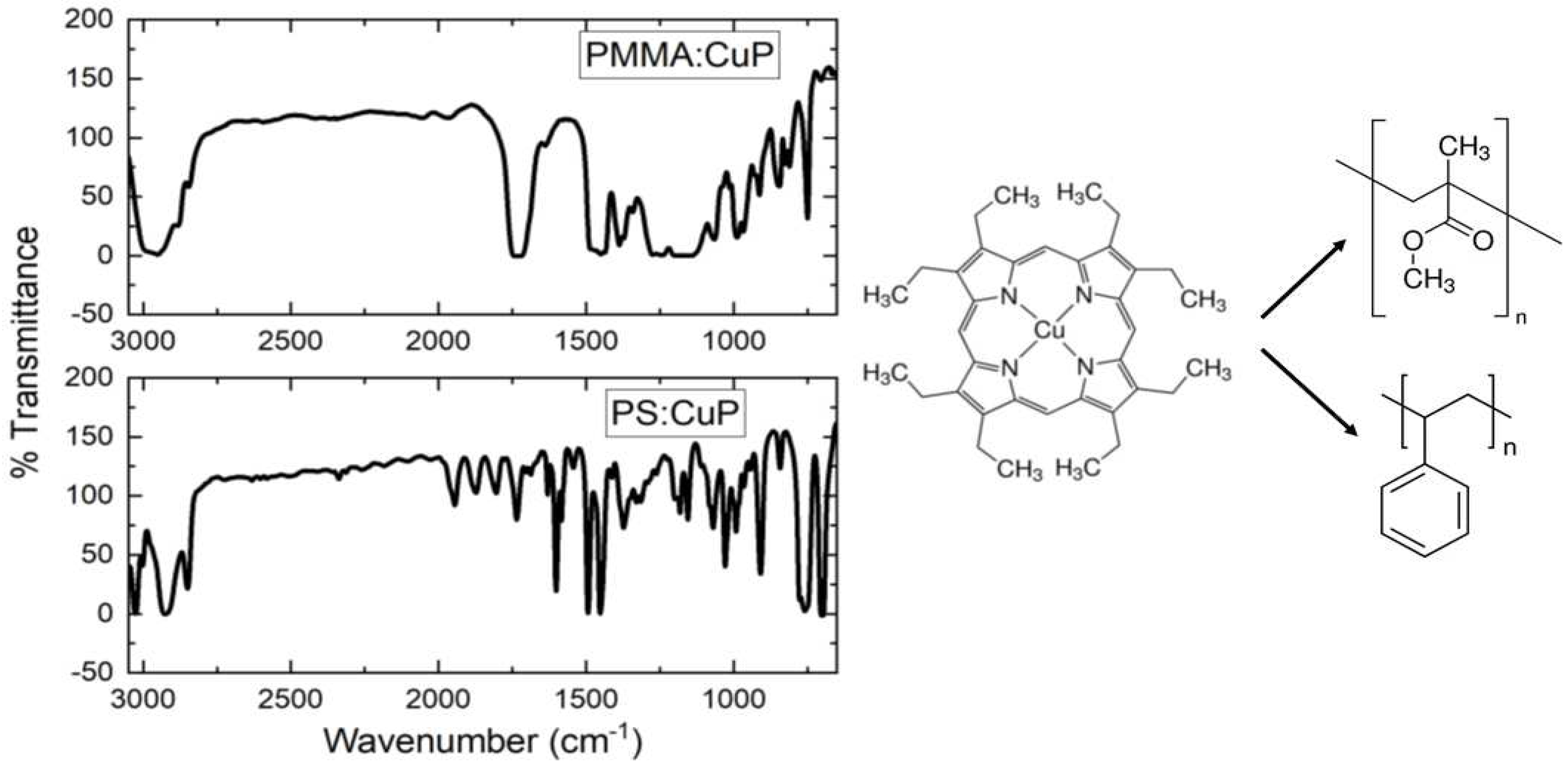
Figure 2.
AFM images of (a) PMMA:CuP and (b) PS:CuP films.
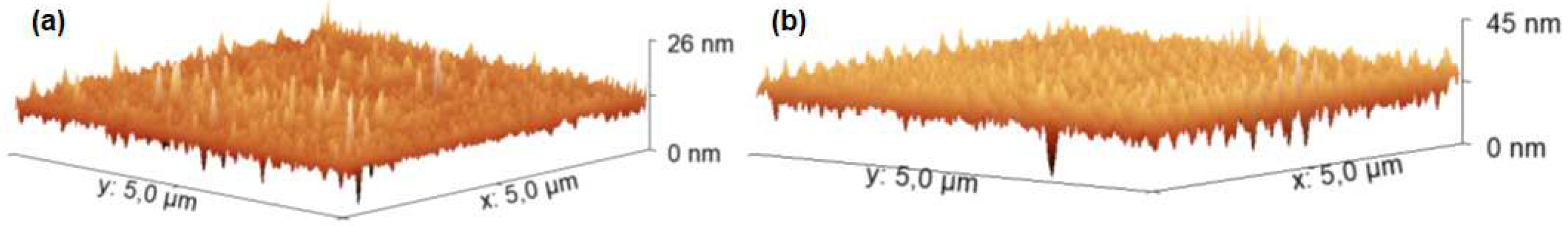
Figure 3.
SEM images of (a) PMMA:CuP and (b) PS:CuP films at 800x.
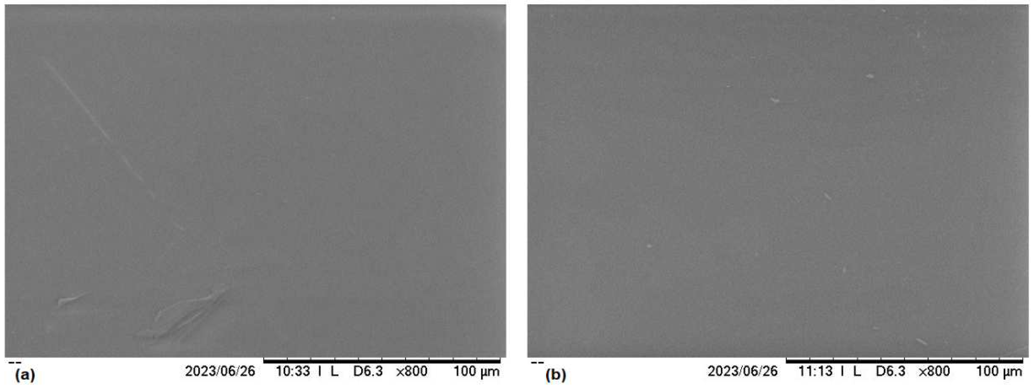
Figure 4.
XRD patterns of polymer:CuP films.
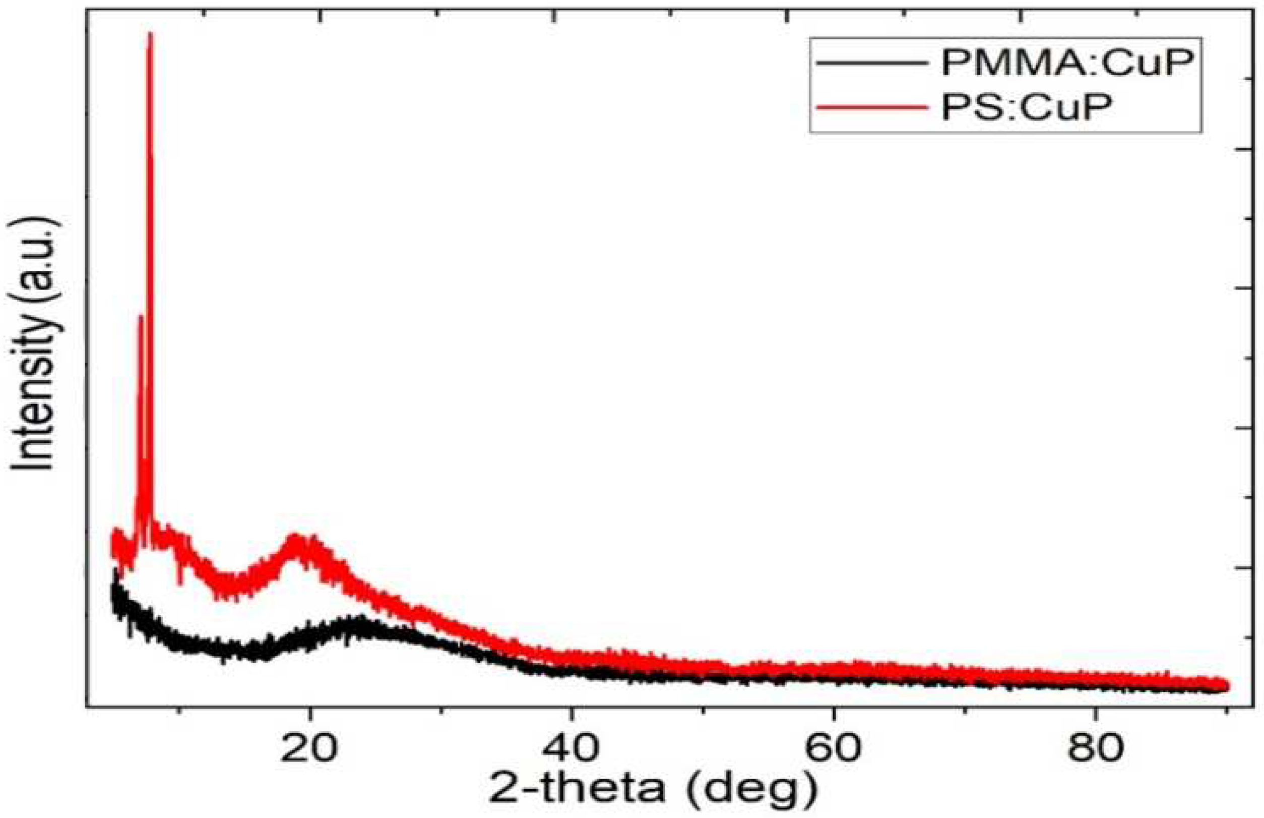
Figure 5.
(a) %Transmittance and (b) absorbance spectra of polymer:CuP films.
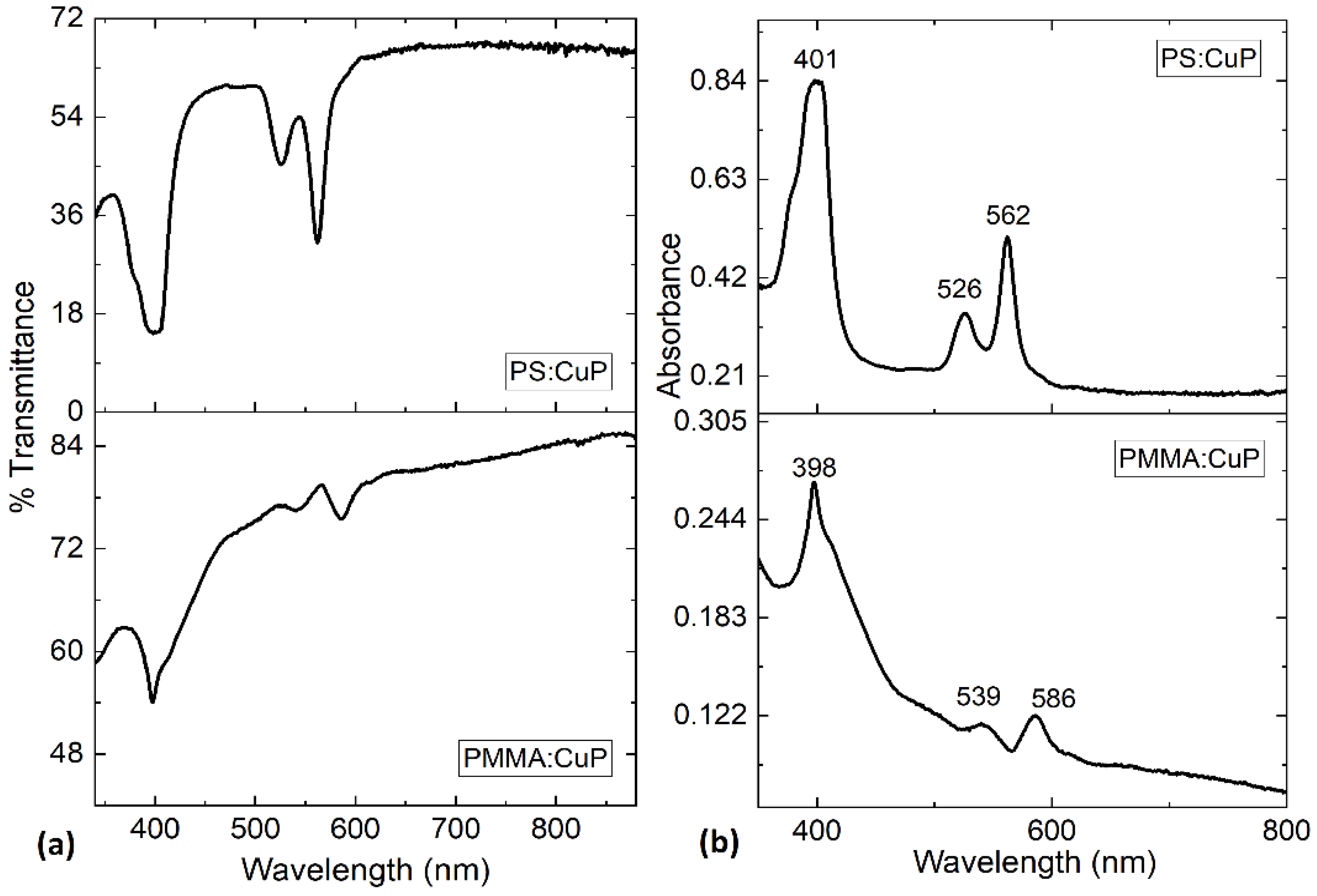
Figure 6.
(a, b) Relation between (αhν)1/2 vs hν energy and (c, d) relation between ln(α) vs hν energy for PMMA:CuP and PS:CuP films.
Figure 6.
(a, b) Relation between (αhν)1/2 vs hν energy and (c, d) relation between ln(α) vs hν energy for PMMA:CuP and PS:CuP films.
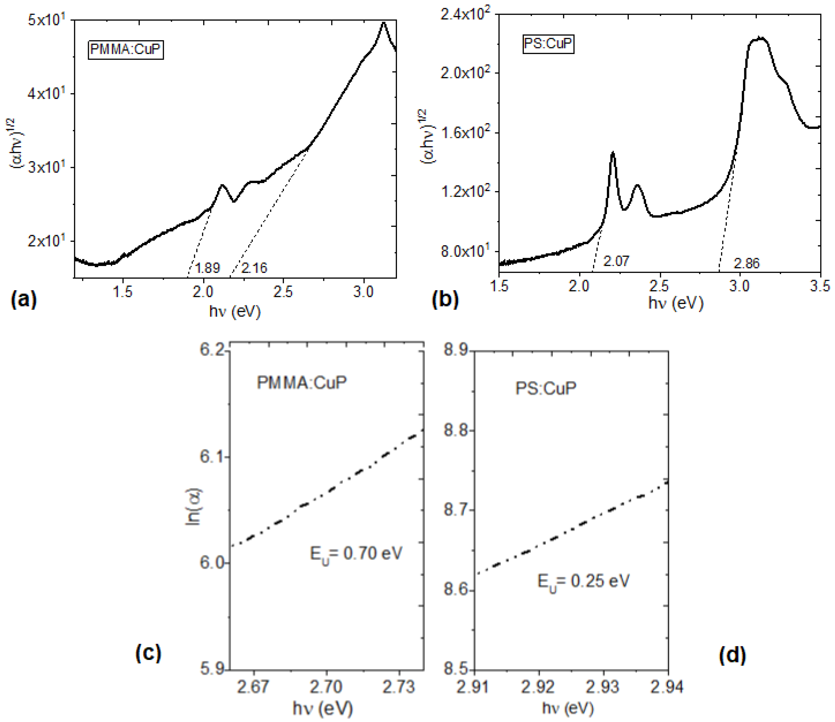
Figure 7.
I-V characteristic curves of the (a) glass/FTO/PMMA:CuP/Ag and (b) glass/FTO/PS:CuP/Ag devices under different incident light color. (c) J-V characteristic curves of glass/FTO/PMMA:CuP/Ag under light and darkness conditions.
Figure 7.
I-V characteristic curves of the (a) glass/FTO/PMMA:CuP/Ag and (b) glass/FTO/PS:CuP/Ag devices under different incident light color. (c) J-V characteristic curves of glass/FTO/PMMA:CuP/Ag under light and darkness conditions.
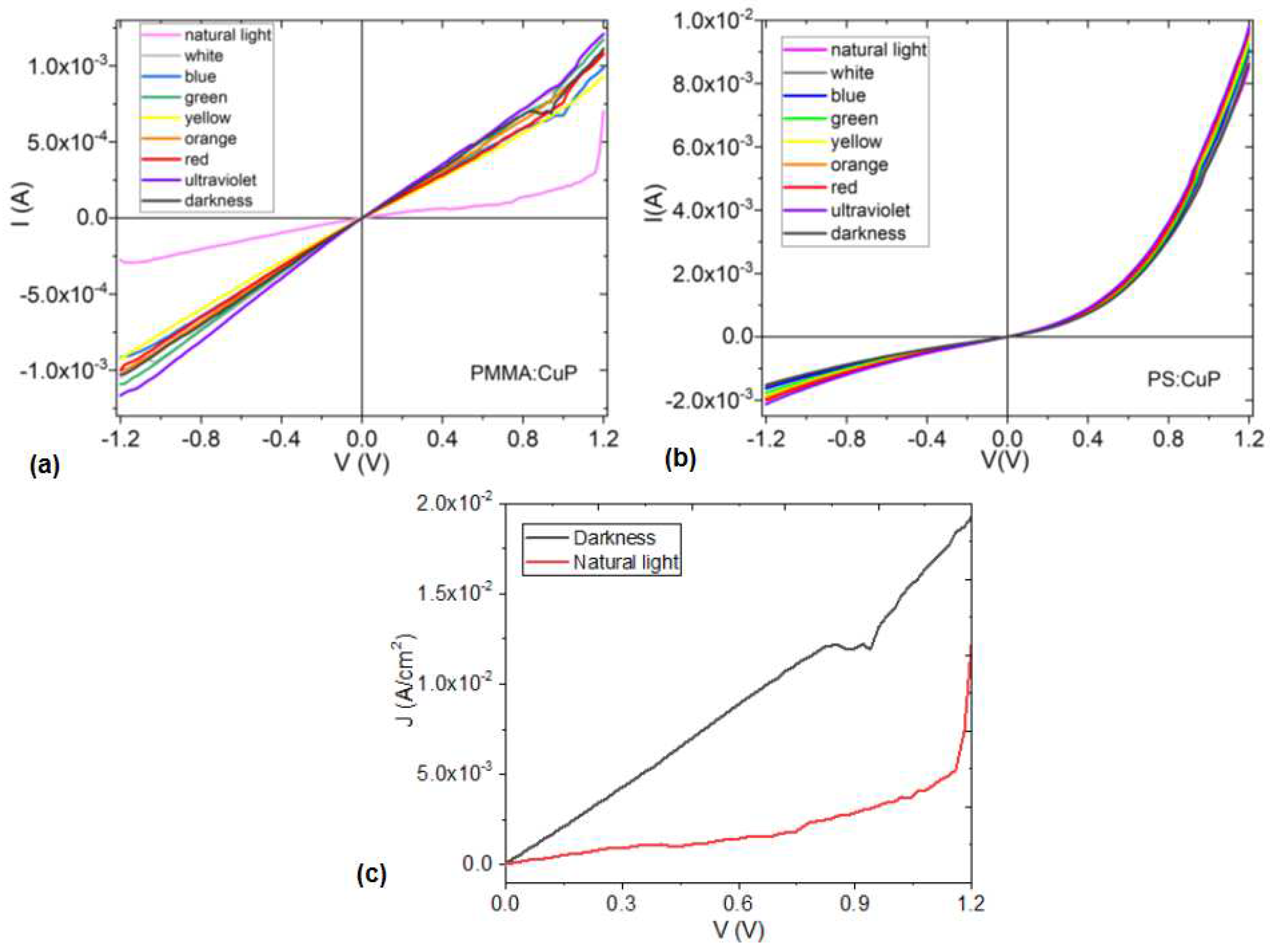

Table 1.
Assignments of polymer-CuP films IR spectra.
| PMMA:CuP (cm-1) |
PS:CuP (cm-1) |
Assignments |
|---|---|---|
| 1445, 1386, 702 | 1437, 1372, 704 | CuP: ν(C-H2)asym |
| 2927 | 2924 | CuP: ν(C-H2)sym |
| 2845 | 2845 | CuP: ν(C-H3)asym |
| 1461 | 1464 | CuP: ν(C-C) |
| 1019 | 1023 | CuP: ν(C-N)pyrrole |
| 1066, 846 | 1066,843 | CuP: ν(N-H) |
| 1739 | PMMA: ν(C=O) | |
| 1637 | PMMA: ν(C=C) | |
| 1134 | PMMA: ν(C-O) | |
| 3026, 2922 | PS: ν(C-H) | |
| 1606 | PS: ν(C=C) | |
| 757 | PS: ν(benzene) |
Disclaimer/Publisher’s Note: The statements, opinions and data contained in all publications are solely those of the individual author(s) and contributor(s) and not of MDPI and/or the editor(s). MDPI and/or the editor(s) disclaim responsibility for any injury to people or property resulting from any ideas, methods, instructions or products referred to in the content. |
© 2023 by the authors. Licensee MDPI, Basel, Switzerland. This article is an open access article distributed under the terms and conditions of the Creative Commons Attribution (CC BY) license (http://creativecommons.org/licenses/by/4.0/).
Copyright: This open access article is published under a Creative Commons CC BY 4.0 license, which permit the free download, distribution, and reuse, provided that the author and preprint are cited in any reuse.


