
Submitted:
06 July 2023
Posted:
10 July 2023
You are already at the latest version
Abstract
Near-infrared (NIR) photodetectors (PDs) have attracted much attention in noninvasive medical diagnosis and treatment. Especially, the self-filtered NIR PDs are highly demandable for tremendous biomedical application due to their strong ability in wavelength discrimination. In this work, we designed and then fabricated a Si micro-holes array/Graphene (Si MHA/Gr) van der Waals (vdW) Schottky NIR photodiode by using PbS quantum dots (QDs) coating. The device exhibits a unique self-filtered NIR response with a responsivity of 0.7 A/W at -1 V and a response time of 61 μs, which are higher than that without PbS QDs coating and even most of previous Si/Gr Schottky photodiodes. The light trapping of the Si MHA and the PbS QDs coating can be attributed to the high responsivity of the vdW photodiode. Furthermore, the presented NIR photodiode can also be integrated in photoplethysmography (PPG) for real-time heart-rate (HR) monitoring. The extracted HR is in great accord with the value measured with the patient monitor by analyzing the Fourier transform of the stable and reliable fingertip PPG waveform, suggesting its potential for practical applications.
Keywords:
Near-infrared photodetectors
; van der Waals Schottky photodiode
; Si micro-holes array
; photoplethysmography
; PdS QDs
1. Introduction
Schottky photodiodes play a key role as devices due to their easy and inexpensive fabrication process, simple device architecture [1,2]. Among these devices, Si-based Schottky photodiodes have drawn attention particularly because of an excellent platform for read-out circuits and large-scale photonic integration [3]. Currently, the novel semi-metal two-dimensional materials (2DMs) have been intensively used to construct the 2DMs/Si van der Waals (vdW) Schottky photodiodes owing to its unique advantages, such as dangling bonds and high transmittance [4,5]. Interestingly, high barrier height and high responsivity can be achieved from Graphene/Si and MXene/Si vdW Schottky photodiodes, which can realize high-performance and low-cost Si-based broadband photodetectors (PDs) [6,7,8]. As is well known, Si-based photodiodes have been a key component for application in near-infrared (NIR) light detection. Nowadays, NIR PDs have attracted much attention in noninvasive medical diagnosis and treatment, including specific molecular detection, imaging, biological detection, light-based diagnostic and therapeutic [9,10,11]. Especially, the self-filtered or narrow-band Si-based NIR PDs are highly demandable for tremendous biomedical application due to their strong ability in wavelength discrimination. For example, a self-filtered NIR Si-based photodoiode was used as photoplethysmography (PPG) sensor for heart rate (HR) monitoring. Notably, a more accuracy HR was achieved than those using broadband PDs of commercial PPG system due to suppression of disturbances caused by ambient light [12]. Due to noninvasive, inexpensive and convenient health monitoring, PPG have become a powerful platform for physiological parameters of individuals monitoring in wearable electronics. The heart rate (HR), blood pressure (BP) and oxygen saturation (SpO2) can be extracted by processing PPG signals, which contains information on arterial blood volume, cardiac, vascular and respiratory [13,14,15]. The NIR light, especially in range of 800~1000 nm, has a higher penetration depth into tissue than visible, enabling physiological signals detected in a wider region [16]. Typically, Si-based NIR PDs can be fabricated for these prerequisites in NIR response by using complex optical systems, inevitably hindering its integration to PPG sensors. Developing a self-filtered Si-based vdW Schottky photodiode with high-performance is imperative and still remains a challenge.
In this paper, we designed and then fabricated a Si micro-holes array/Graphene (Si MHA/Gr) van der Waals (vdW) Schottky photodiode by PbS QDs coating. The Si MHA and PbS QDs were used to improve the NIR absorption and photoresponse. The PbS QDs coated vdW Schottky photodiode possesses a self-filtered NIR response with a responsivity of 0.7 A/W at -1 V and a response time of 61 μs, which are higher than most of previous 2DMs/Si vdW Schottky photodiodes in the range of NIR light. Furthermore, the stable and reliable fingertip photoplethysmogram (PPG) signals were achieved based on our self-setup PPG system by using the PbS QDs coated vdW Si MHA/Gr vdW Schottky photodiode. The further extracted heart-rate based on the PPG signals is in great accord with patient monitor by analyzing the Fourier transform of the PPG waveform.
2. Materials and Methods
TCAD simulations. The Silvaco TCAD was used for the design of the silicon micro-holes-based NIR Schottky photodiode. The simulation and analysis of the devices were carried out using this software (Altas, Tonyplot).
Device fabrication. The PbS coated Si MHA/Gr vdW Schottky photodiode fabrication process is presented in Figure 1a. A double sides polished silicon wafer (n-type, 0.01-1 Ωcm-1) was chosen. The Si MHA (diameter~10 μm, spacing~20 μm) was firstly defined on one side of silicon substrate using a UV lithography, and was then etched by using inductively coupled plasma system (ICP, ICP-601) with HBr/Cl2/O2 (100/50/50 sccm) mixtures for 30 min. The chamber pressure was kept at 10 Pa and the inductive power and chuck bias power were maintained at 120 W and 100 W, respectively. Afterwards, the remaining photoresist mark was removed by using a cleaning stripper. Subsequently, the chemistry vapor deposition (CVD)-grown bilayer graphene (Hefei Vigon Material Technology Co., Ltd.) was transferred to the other side of the silicon substrate as the Schottky contact electrode. A hollow circular In/Ga bilayer paste electrode was formed on after-etching micro-holes array, serving as an ohmic contact electrode and the light illumination window (diameter of ~5 mm). PbS QDs were synthesized by following previously reported work [17,18,19], and the PbS QDs film was then formed on the top of Si MHA by spin-coating method. The device was then mounted on a printed circuit board for the following measurement. The height of the micro-holes was measured by a step profiler (Dektak XT). The absorption spectra of the device were measured by a UV–vis–NIR spectrophotometer (SHIMADZU UV-3600). The images were obtained by using a field-emission scanning electron microscope (SEM, SU8020).
Device characterization. The electrical and optical characteristics of the vdW Schottky photodiodes were measured using a semiconductor analyzer (4200-SCS, Keithley). The laser diodes (254 nm, 365 nm, 405 nm, 650 nm, 808 nm, 980 nm, 1064 nm) were used as light sources to obtain the responsivity of the device. The incident power was defined on the detector active area and calibrated using a Thorlabs PM100D optical power meter.
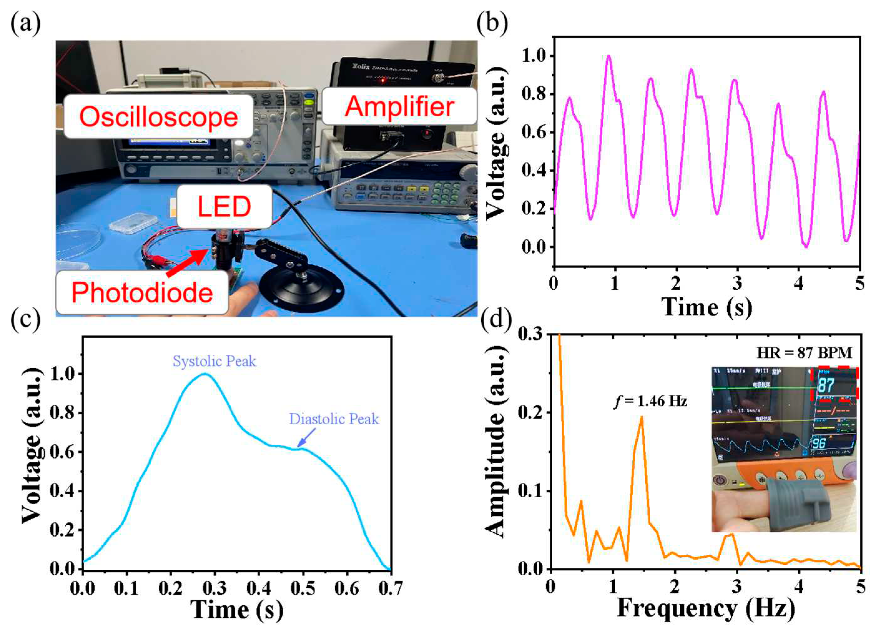
PPG heart-rate measurement. The PPG heart-rate measurement was carried out using the PbS QDs coated Si MHA/Gr vdW Schottky photodiode, an amplifier, a LED (980 nm) and a digital oscilloscope (GDS-1072B, RIGOL), as seen in Figure 6a. The heartbeat waveform of the same person was simultaneously recorded by a digital oscilloscope from this heart-rate measurement system and a patient monitor. (UT4000Apro, GOLDWAY)
3. Results and Discussion
Figure 1a illustrates the fabrication process of the PbS QDs coated Si MHA/Gr vdW Schottky NIR photodiode, in which inductively coupled plasma (ICP) technique, the well-developed silicon etching technique, was chosen to obtain Si MHA [8,12]. The CVD-graphene was used to form Schottky contact as bottom electrode. The top In/Ga paste electrode was made on the silicon surface all around to form good ohmic contact with n-type silicon, together with keeping high transparency. The photodioode was then mounted in a circuit board for photoresponse characteristics evaluation and following practical application in PPG heart-rate monitoring. Figure 1b shows the as-ICP etched Si MHA image, indicating a good uniformity of the micro-holes array with a diameter of 15 μm and depth of 2.5 μm (Figure 1c).The diameter variation of the micro-hole can be attributed to the lateral etching on the silicon surface due to the longer etching time. From the TEM image of the PbS QDs (Figure 1d), a uniform QDs with a diameter of ~12 nm can be found. Besides, the absorption of the PbS QDs shown in Figure 1e indicates the excellent NIR absorption, which can be used to enhance the NIR response for the Si-based photodetectors.
Figure 2a shows the band energy diagram of the Si MHA/Gr NIR vdW Schottky photodiode, the electron-hole carriers are generated near the junction and then separated and thereby collected by electrode under NIR light illumination. Figure 2b shows the I–V curves of the phododiode in the dark, showing an rectification behavior. Detailed characterization reveals a Schottky barrier height (ΦB) of 0.50 eV and an ideal factor (n) of 1.9, which are helpful for separating photogenerated carriers. In order to investigate the photoresponse characteristics, Figure 2c plots I-V curves of the photodiode measured under UV, visible and NIR light illumination with the same incident light power (Pin) of 1.7 mW. Notably, the photodiode shows an sensitivity to NIR light and no obvious response to UV and visible light, which is different from previous Si-based Schottky photodiodes with a broadband response [20,21,22]. Significantly, from the normalized response (Figure 2d), the photodiode exhibits a self-filtered NIR response with a signal to noise ratio (SNR) in the range of 102~103 to visible light and UV light, indicating a strong ability on wavelength discrimination. The unique self-filtered NIR response can attributed to the device structure of back illuminated Schottky junction, which will be discussed in the following.
To investigate the enhanced photoresponse characteristics of the PbS QDs coating, the I-V curves of these photodiodes with and without PbS QDs coating under 1064 nm light illumination are shown in Figure 3a, respectively. It was clear that the photocurrent (IP~0.1 mA) of the photodiode with PbS QDs coating is higher than that of photodiode without PbS QDs coating (~0.028 mA) at bias voltage of -2 V. To further determine the device performance, Figure 3b plots the I-V curves of the photodiode under 1064 nm incident light illumination with power in the range of 0.017 mW~2.04 mW, suggesting photoresponse related to the incident light power. Apparently, the photodiode shows a photovoltaic behavior, indicating the photodiode can be as a self-powered photodetector. Besides, the time dependent response curves for the photodiodes with and without PbS QDs coating at bias voltage of -1 V under 1064 nm light illumination with different light power are plotted in Figure 3c, showing a stability current ON/OFF ratio (ION/IOFF) up to 102. Besides, we calculated the light power-dependent responsivity (R) as shown (Figure 3d), which can be expressed as
R =Ip/Pin
It is apparent that the R increases with Pin decreasing, and reaches up to 0.72 A/W and 0.2 A/W at bias voltage of -1 V and 0 V, respectively, showing an remarkable enhancement about 2 times by comparing with the values of the photodiode without PbS QDs coating. The PbS QDs coated Si MHA/Gr vdW photodiode exhibits a higher responsivity for NIR light than those previous Gr/Si Schottky photodiodes and even commercial Si-based photodiodes [23,24,25]. Particularly, the device can be operated at self-powered mode due to the high responsivity and high ION/IOFF of ~105 , which can be estimated in Figure 3b .
The enhanced responsivity and self-filtered NIR response of the PbS QDs coated Si MHA/Gr vdW Schottky photodiode are related to be the structure of the Si MHA and the PbS QDs coating. Figure 4a compares the incident light (λ) dependent R curves of planar Si/Gr, Si MHA/Gr and PbS QDs coated Si MHA/Gr photodiodes under light power of 0.017 mW at bias voltage of 0 V. It can be clearly seen that the calculated R of PbS QDs coated Si MHA/Gr photodiode shows an improvement about 9.5 and 2.8 times by comparing with those of planar Si/Gr and Si MHA/Gr, respectively. Therefore, both Si MHA and PbS QDs can be beneficial to improve NIR response based on our study, which can attributed to the improvement of NIR light absorption, as shown in Figure 4b. The TCAD-simulated optical intensity distribution was used to understand the mechanism, indicating a obvious light trapping effect of the Si MHA (Figure 4c). Furthermore, the absorption of the PbS QDs in NIR can be also benefit for NIR response (Figure 1e). Otherwise, we can also explore the mechanism about self-filtered NIR response of the photodiode based on the simulated optical intensity distribution. From the Figure 4c, we can find that long-wavelength NIR lights (e.g. 980, 1064 nm) can penetrate to the bottom Schottky junction, while the visible lights (e.g. 520, 650 nm) will be absorbed by Si surface due to the absorption coefficient (α) of the Si [26]. When NIR light illuminated on the photodiode, the photocarriers can be generated near the junction and then separated and collected by Schottky built-in electric field, thus inducing photocurrent. Due to visible light absorbed near the Si top surface, most of photocarriers will be recombines because of the diffusion length of the carriers [27], resulting in extremely low photocurrent.
Finally, we explicitly investigate the optical bandwidth and response speed of the photodiode. The normalized response characteristics versus pulsed light frequency (f) curve of the photodiode at zero bias voltage is shown in Figure 5a. The 3-dB optical bandwidth is estimated to be 2.0 kHz, which is comparable to most of reported Gr/Si photodiodes [28]. Notably, the photodiode can well follow the pulse light at f=2 kHz (Figure 5b) and even f=8 kHz (Figure 5c), suggesting the photodiode can well follow the light with high pulsed frequency. From the magnified plot for a single photovoltage cycle (Figure 5d) at f=2 kHz, the rise time (τr) and fall time (τf) are estimated to be 61 μs and 206 μs, which are also comparable to most of reported Gr/Si or Si-based heterojunction photodiodes [28].
The high-performance and self-filtered NIR response of the PbS coated Si MHA/Gr vdW Schottky NIR photodiode show great potential in biomedical measurement. We build a transmitted PPG heart pulse monitoring system, which composed a 980 nm LED, an amplifying circuit and an oscilloscope, as shown in Figure 6a. In this system, the 980 nm LED was used as the light source because the transmission of tissue is the greatest in the range of 800-1000 nm. The PbS coated Si MHA/Gr vdW Schottky NIR photodiode was used as the sensor to detect NIR light signal of the transmitted tough finger tissue. Vascular blood flow will induce the transmitted light changes, which can be detected by vdW Schottky photodiode and then amplified photovoltage will be simultaneously recorded by an oscilloscope. Figure 6b shows the heart pulse waveform from our heart pulse monitoring system. It can be find that the PPG waveform was successfully achieved in our measurement. Especially, the waveform possesses a featured peak, such as systolic and diastolic peak (Figure 6c), suggesting a reliable PPG waveform which is benefit for the subsequent physiological parameters of individuals, such as HR and BP. To accurately estimate the value of the heart rate, a PPG waveform was transformed by Fourier transform, as shown in Figure 6d. The HR is estimated to be 87 beats per minute (BPM), which is in great accord with the value measured by the commercial patient monitor (inset in Figure 6d). The result suggests that the PbS coated Si MHA/Gr vdW Schottky NIR photodiode shows a potential application in PPG system to obtain reliable PPG waveform for heart rate measurement.
4. Conclusions
In summary, a PbS coated Si MHA/Gr vdW Schottky NIR photodiode was successfully fabricated. Compared with previous Si-based Schottky photodiodes, the device exhibits a unique self-filtered NIR response with a responsivity of 0.7 A/W at -1 V and a response time of 61 μs, which are higher than that without PbS QDs coating and even most of previous Si/Gr photodiodes. The device structure, the Si MHA and PbS QDs coating can be attributed to the NIR response. The presented photodiode was used as the PPG sensor, and a reliable and featured PPG waveform can be obtained. The extracted HR based on analyzing the Fourier transform of the PPG waveform is in great accord with the value measured by the patient monitor, suggesting its potential for practical applications for real-time heart-rate (HR) monitoring. Our work opens a new avenue for the fabrication of high-performance NIR Schottky photodiodes for PPG heart-rate monitoring.
5. Patents
This work was supported by Open Research Fund of State Key Laboratory of Pulsed Power Laser Technology (No. SKL2019KF09).
Acknowledgments
Y.Q. Yu thanks Qingyan Yang for help in support of a patient monitor for heart rate measurement.
References
- Tao, A.; Yao, T.; Jiang, Y.; Yang, L.; Yan, X.; Ohta, H.; Ikuhara, Y.; Chen, C.; Ye, H.; Ma, X. Single-dislocation Schottky diodes. Nano Lett. 2021, 21, 5586–5592. [Google Scholar] [CrossRef]
- Chang, K.E.; Yoo, T.J.; Kim, C.; Kim, Y.J.; Lee, S.K.; Kim, S.Y.; Heo, S.; Kwon, M.G.; Lee, B.H. Gate-controlled graphene–silicon Schottky junction photodetector. Small 2018, 14, 1801182. [Google Scholar] [CrossRef]
- Yang, W.; Chen, J.X.; Zhang, Y.; Zhang, Y.J., He; Fang, X.S. Silicon-compatible photodetectors: Trends to monolithically integrate photosensors with chip technology. Adv. Funct. Mater. 2019, 29, 1808182. [Google Scholar] [CrossRef]
- Liu, C.; Guo, J.; Yu, L.; Li, J.; Zhang, M.; Li, H.; Shi, Y.; Dai, D. Silicon/2D-material photodetectors: From near-infrared to mid-infrared. Light: Sci. Appl. 2021, 10, 123. [Google Scholar] [CrossRef] [PubMed]
- Kang, Z.; Ma, Y.; Tan, X.; Zhu, M.; Zheng, Z.; Liu, N.; Li, L.; Zou, Z.; Jiang, X.; Zhai, T.; et al. MXene–silicon van der Waals heterostructures for high-speed self-driven photodetectors. Adv. Electron. Mater. 2017, 3, 1700165. [Google Scholar] [CrossRef]
- Wan, X.; Xu, Y.; Guo, H.; Shehzad, K.; Ali, A.; Liu, Y.; Yang, J.; Dai, D.; Lin, C.; Liu, L.; et al. A self-powered high-performance graphene/silicon ultraviolet photodetector with ultra-shallow junction: Breaking the limit of silicon? NPJ 2D Mater. Appl. 2017, 1, 4. [Google Scholar] [CrossRef]
- Song, W.; Liu, Q.; Chen, J.; Chen, Z.; He, X.; Zeng, Q.; Li, S.; He, L.; Chen, Z.; Fang, X. Interface engineering Ti3C2 MXene/silicon self-powered photodetectors with high responsivity and detectivity for weak light applications. Small 2021, 17, 2100439. [Google Scholar] [CrossRef] [PubMed]
- Song, L.; Xu., E.; Yu, Y.; Jie, J.; Xia, Y.; Chen, S.; Jiang, Y.; Xu, G.; Li, D.; Jie, J. High-barrier-height Ti3C2Tx/Si microstructure Schottky junction-based self-powered photodetectors for photoplethysmographic monitoring. Adv. Mater. Technol. 2022, n/a, 2200555. [Google Scholar] [CrossRef]
- Ollearo, R.; Ma, X.; Akkerman, H.B.; Fattori, M.; Dyson, M.J.; van Breemen, A.J.J.; Meskers, S.C.J.; Dijkstra, W.; Janssen, R.A.J.; Gelinck, G.H. Vitality surveillance at distance using thin-film tandem-like narrowband near-infrared photodiodes with light-enhanced responsivity. Sci. Adv. 2023, 9, eadf9861. [Google Scholar] [CrossRef]
- Simone, G.; Tordera, D.; Delvitto, E.; Peeters, B.; van Breemen, A.J.J.; Meskers, S.C.J.; Janssen, R.A.J.; Gelinck, G.H. High-accuracy photoplethysmography array using near-infrared organic photodiodes with ultralow dark current. Adv. Opt. Mater. 2020, 8, 1901989. [Google Scholar] [CrossRef]
- Nowara, E.M.; Marks, T.K., Mansour; Veeraraghavan, A. near-infrared imaging photoplethysmography during driving. IEEE Trans. Intell. Transp. Syst. 2022, 23, 3589–3600. [Google Scholar] [CrossRef]
- Zhang, H.; Cui, Y.; Lu, M.; Yang, Q.; Feng, J.; Chen, S.; Yang, X.; Xu, G.; Yu, Y. Self-filtered NIR photodetectors based on silicon micro-holes array for stable heart rate monitoring. IEEE Electron Device Lett. 2022, 43, 2129–2132. [Google Scholar] [CrossRef]
- Charlton, P.H.; Kyriacou, P.A.; Mant, J.; Marozas, V.; Chowienczyk, P.; Alastruey, J. Wearable Photoplethysmography for cardiovascular monitoring. Proc. IEEE 2022, 110, 355–381. [Google Scholar] [CrossRef]
- Sun, Y.; Thakor, N. Photoplethysmography revisited: From contact to noncontact, from point to imaging. IEEE Trans. Biomed. Eng. 2016, 63, 463–477. [Google Scholar] [CrossRef] [PubMed]
- Spigulis, J.; Gailite, L.; Lihachev, A.; Erts, R. Simultaneous recording of skin blood pulsations at different vascular depths by multi-wavelength photoplethysmography. Appl. Opt. 2007, 46, 1754–1759. [Google Scholar] [CrossRef]
- Xu, H.; Liu, J.; Zhang, J.; Zhou, G.; Luo, N.; Zhao, N. Flexible organic/inorganic hybrid near-Infrared photoplethysmogram sensor for cardiovascular monitoring. Adv. Mater. 2017, 29, 1700975. [Google Scholar] [CrossRef]
- Mi, L.; Chang, Y.; Zhang, Y.; Xu, E.; Jiang, Y. Hybrid perovskite exchange of PbS quantum dots for fast and high-detectivity visible–near-infrared photodetectors. J. Mater. Chem. C 2021, 9, 417–438. [Google Scholar] [CrossRef]
- Mi, L.; Wang, H.; Zhang, Y.; Yao, X.; Chang, Ya.; Li, G.; Lei, C.; Li, G.; Jiang, Y. Converting electrical conductivity types in surface atomic-ligand exchanged PbS quantum dots via gate voltage tuning. J. Alloys Compd. 2017, 699, 866–873. [Google Scholar] [CrossRef]
- Mi, L.; Wang, H.; Zhang, Y.; Yao, X.; Chang, Y.; Li, G.; Li, G.; Jiang, Y. High performance visible–near-infrared PbS-quantum-dots/indium Schottky diodes for photodetectors. Nanotechnology. 2017, 28, 055202. [Google Scholar] [CrossRef] [PubMed]
- Lv, P.; Zhang, X.; Zhang, X.; Deng, W.; Jie, J. High-sensitivity and fast-response graphene/crystalline silicon Schottky junction-based near-IR photodetectors. IEEE Electron Device Lett. 2013, 34, 1337–1339. [Google Scholar] [CrossRef]
- Xiang, D.; Han, C.; Hu, Z.; Lei, B.; Liu, Y.; Wang, L.; Hu, W.; Chen, W. Surface transfer doping-induced, high-performance graphene/silicon Schottky junction-based, self-powered photodetector. Small 2015, 11, 4829. [Google Scholar] [CrossRef] [PubMed]
- Li, X.; Zhu, M.; Du, M.; Lv, Z.; Zhang, L.; Li, Y.; Yang, Y.; Yang, T.; Li, X.; Wang, K.; et al. Graphene: High detectivity graphene-silicon heterojunction photodetector. Small 2016, 12, 549–549. [Google Scholar] [CrossRef]
- Adhikari, S.; Biswas, C.M.H.; Doan, M.H.; Kim, S.T.; Kulshreshtha, C.; Lee, Y.H. Minimizing trap charge density towards an ideal diode in graphene-silicon Schottky solar cell. ACS Appl. Mater. Interfaces 2019, 11, 880–888. [Google Scholar] [CrossRef]
- Periyanagounder, D.; Gnanasekar, P.; Varadhan, P.; He, J.H.; Kulandaivel, J. High performance, self-powered photodetectors based on a graphene/silicon Schottky junction diode. J. Mater. Chem. C 2018, 6, 9545–9551. [Google Scholar] [CrossRef]
- Yin, J.; Liu, L.; Zang, Y.; Ying, A.; Hui, W.; Jiang, S.; Zhang, C.; Yang, T.; Chueh, Y.L.; Li, J.; et al. Engineered tunneling layer with enhanced impact ionization for detection improvement in graphene/silicon heterojunction photodetectors. Light: Sci. Appl. 2021, 10, 113. [Google Scholar] [CrossRef] [PubMed]
- Wang, L.; Luo, H.; Zuo, H.J.; Tao, J.; Yu, Y.; Yang, X.; Wang, M.; Hu, J.; Xie, C.; Wu, D.; et al. Highly sensitive narrowband si photodetector with peak response at around 1060 nm IEEE Trans. Electron Devices 2020, 67, 3211–3214. [Google Scholar] [CrossRef]
- Wang, L.; Li, Z.; Li, M.; Li, S.; Lu, Y.; Qi, N.; Zhang, J.; Xie, C.; Wu, C.; Luo, L.B. Self-powered filterless narrow-band p–n heterojunction photodetector for low background limited near-infrared image sensor application, ACS Appl. Mater. Interfaces 2020, 12, 21845–21853. [Google Scholar] [CrossRef] [PubMed]
- Yu, Y.; Li, Z.; Lu, Z.J.; Geng, X.; Lu, Y.; Xu, G.; Wang, L.; Jie, J. Graphene/MoS2/Si nanowires Schottky-NP bipolar van der waals heterojunction for ultrafast photodetectors. IEEE Electron Device Lett. 2018, 39, 1688–1691. [Google Scholar] [CrossRef]
Figure 1.
(a) Schematic illustration of the fabrication process for PbS QDs coated Si MHA/Gr vdW Schottky NIR photodiode. (b) SEM image of the Si MHA. (c) The depth curve of Si MHA. (d) TEM image of the PbS QDs. (e) The absorption of PbS QDs.
Figure 1.
(a) Schematic illustration of the fabrication process for PbS QDs coated Si MHA/Gr vdW Schottky NIR photodiode. (b) SEM image of the Si MHA. (c) The depth curve of Si MHA. (d) TEM image of the PbS QDs. (e) The absorption of PbS QDs.
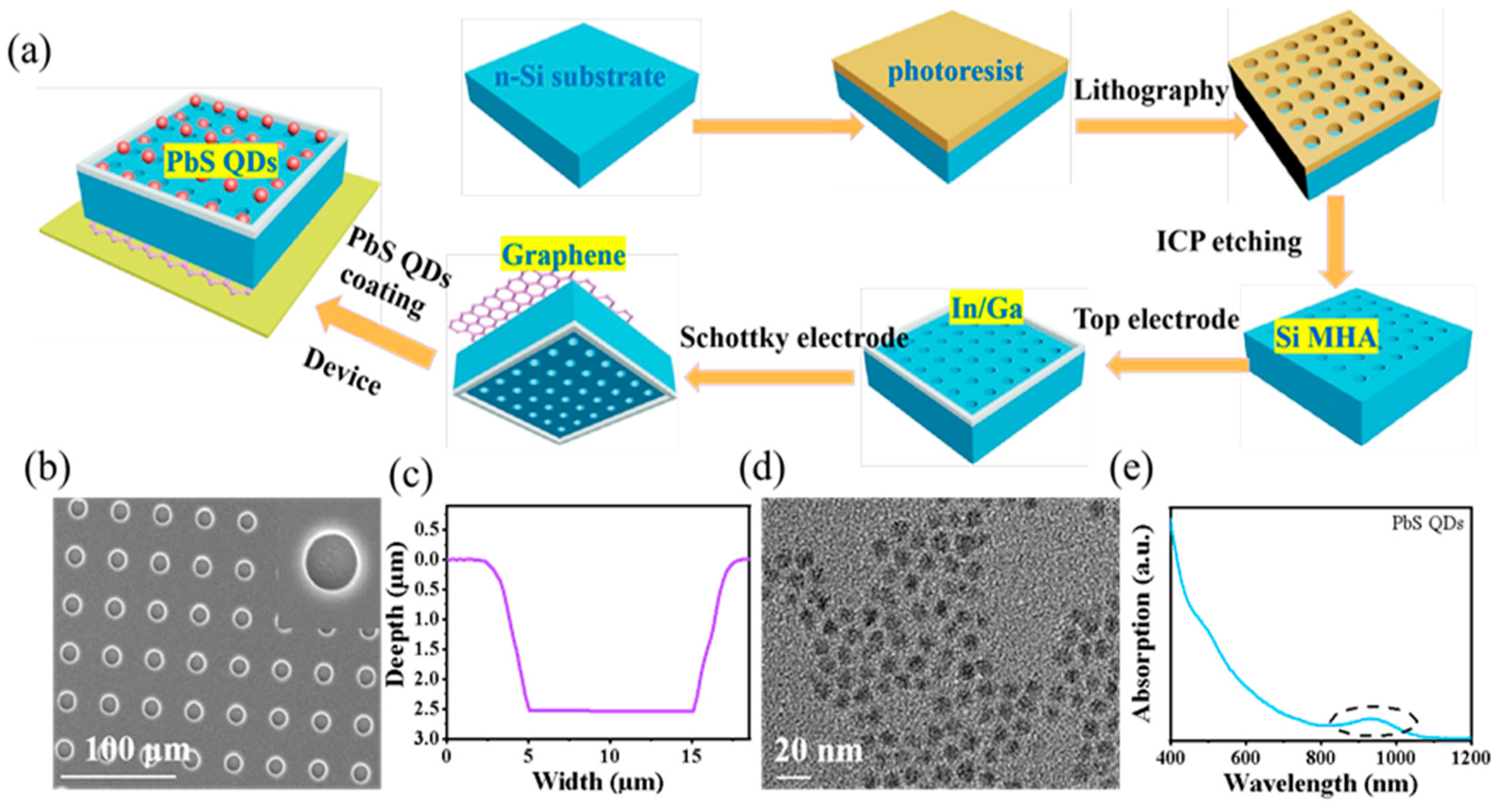
Figure 2.
(a) The band energy diagram of the Si MHA/Gr NIR vdW Schottky photodiode. (b) I-V curves of the photodiode in the dark. (c) I-V curves of the photodiode under different light illumination and dark under light intensity of 1.7 mW, respectively. (d) The normalized response.
Figure 2.
(a) The band energy diagram of the Si MHA/Gr NIR vdW Schottky photodiode. (b) I-V curves of the photodiode in the dark. (c) I-V curves of the photodiode under different light illumination and dark under light intensity of 1.7 mW, respectively. (d) The normalized response.
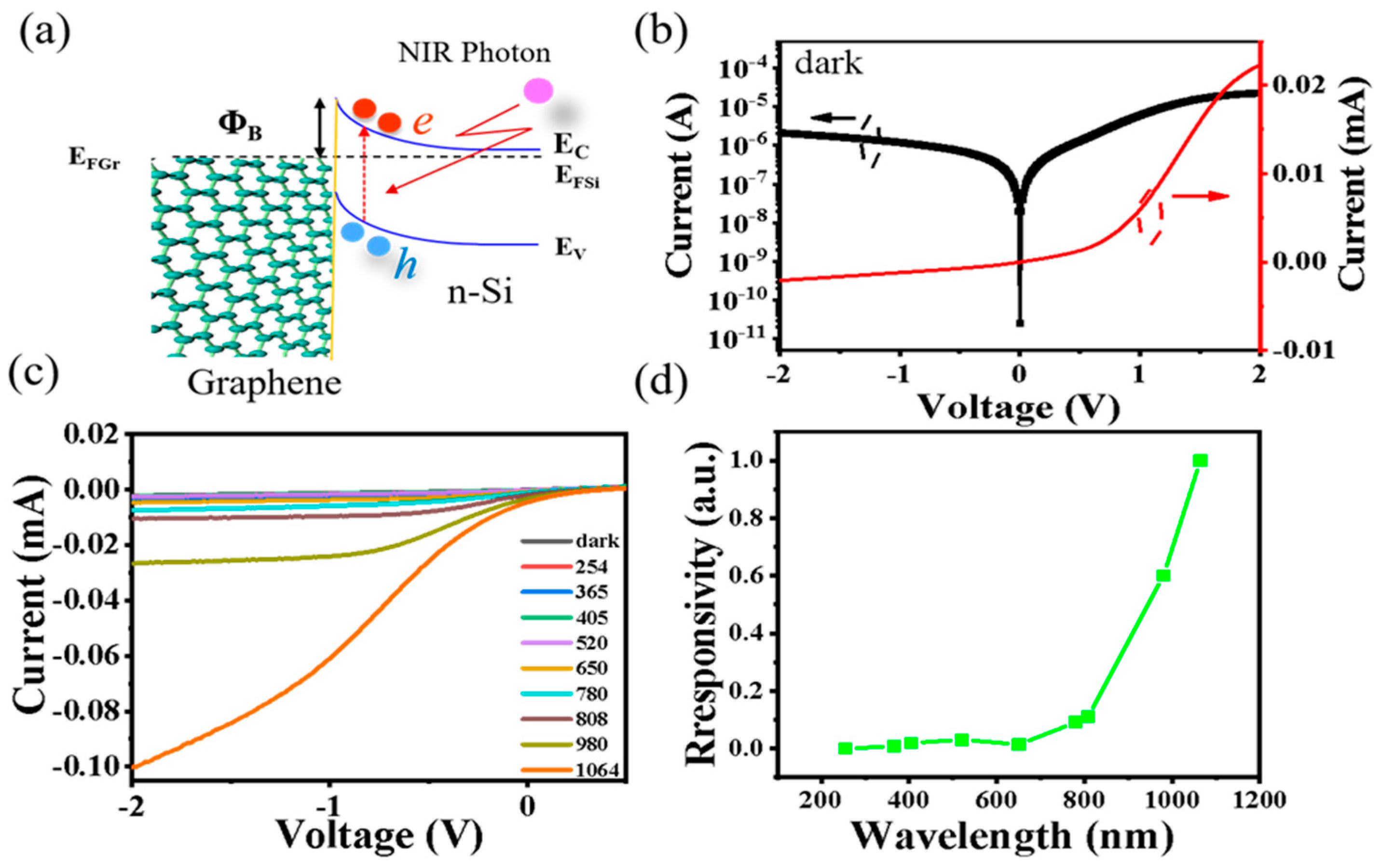
Figure 3.
(a) I-V curves of the vdw Schottky photodiodes with and without PbS QDs coating and in the dark and 1064 nm light illumination, respectively. (b) I-V curves of the photodiode with PbS QDs coating under 1064 nm light illumination with varied light power. (c) The time response of the photodiodes with and without PbS QDs coating under varied light power illumination. (d) The light power dependent responsivity curves of the photodiodes with and without PbS QDs coating at bias of 0 V and -1 V, respectivity.
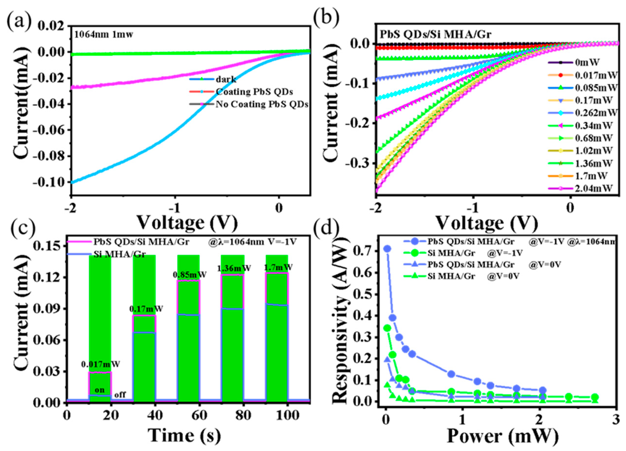
Figure 4.
(a) The wavelength dependent responsivity for planar Si/Gr, Si MHA/Gr and PbS QDs coated Si MHA/Gr photodiodes, respectively. (b) The absorption of Si MHA and planar Si. (c) The absorption of PbS QDs. (d) The simulated optical intensity distribution of the Si MHA/Gr and plane Si/Gr Schottky junction under defferent light illumination, respectively.
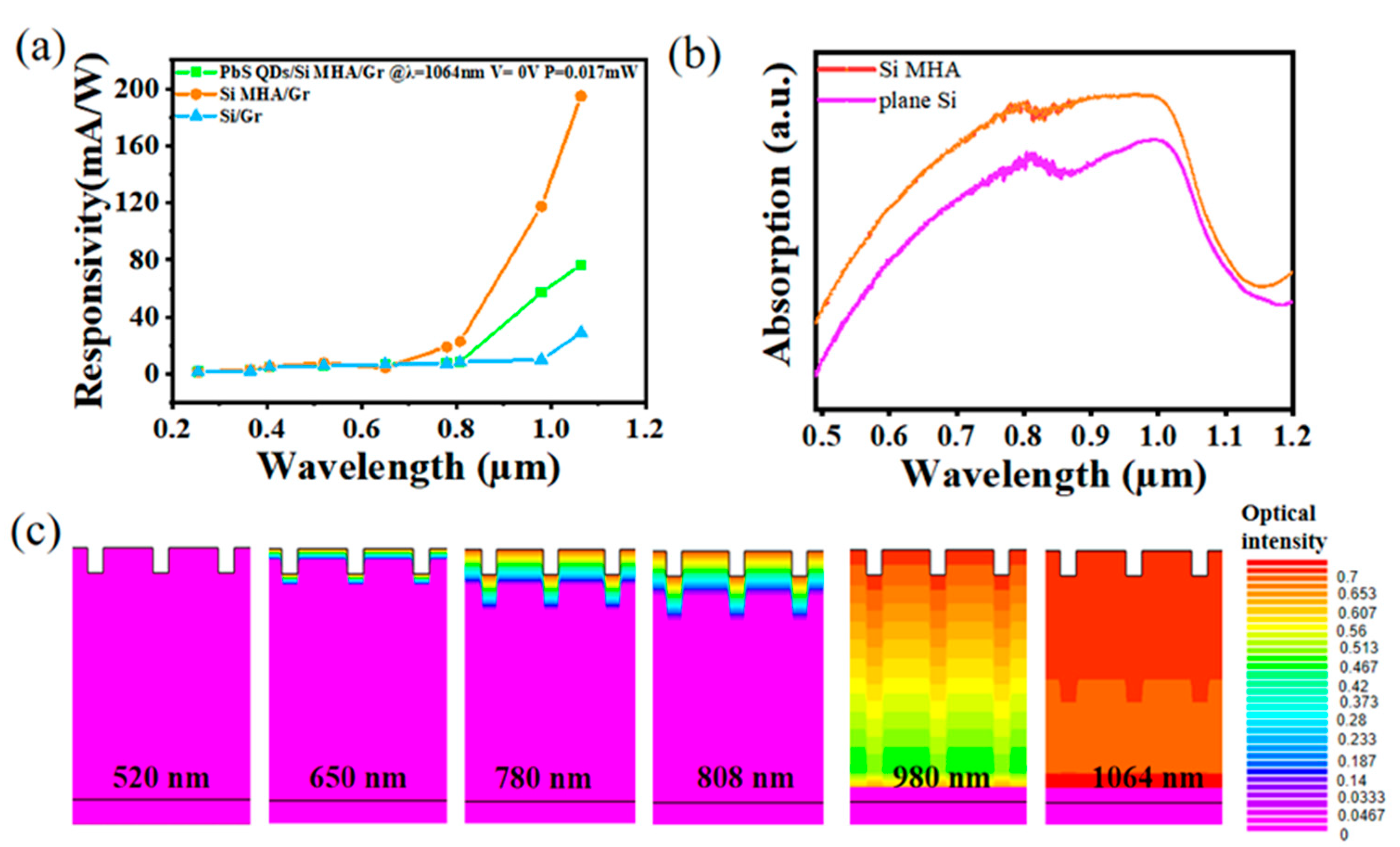
Figure 5.
(a) Normalized response characteristics versus frequency (f) curves of the PbS coated Si MHA/Gr vdW Schottky photodiode at zero bias voltage. Normalized time response of these photodiodes at f=100 Hz and 2 kHz (b) and (c) 8 kHz. (d) Magnified plot of one response cycle of the photodiode for estimating the response time.
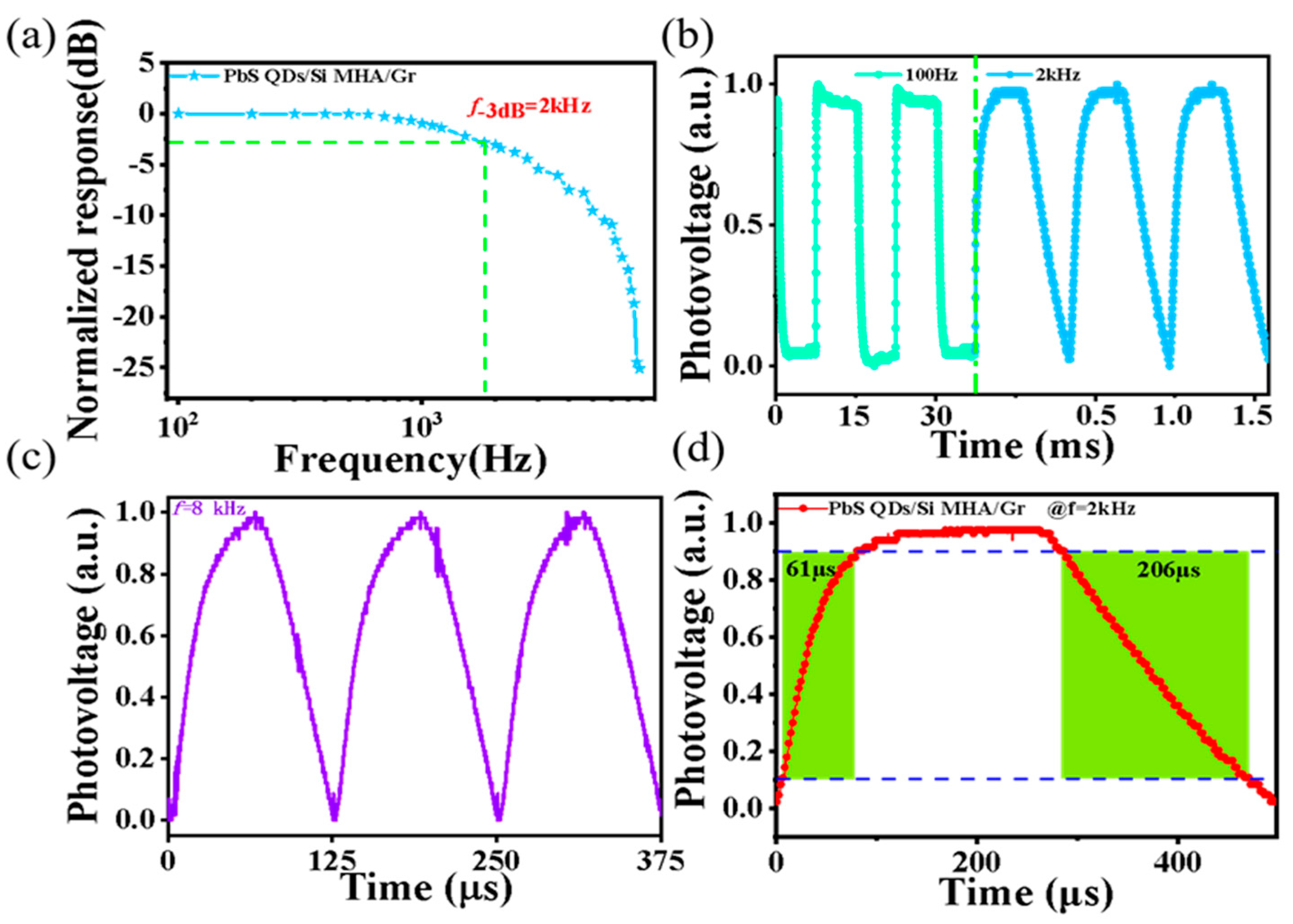
Figure 6.
(a) Schematic illustration and photograph of the PbS coated Si MHA/Gr vdW Schottky photodiode for PPG measurement. (b) The obtained PPG waveform. (c) A typical PPG waveform from (b), showing systolic peaks and diastolic peak. (d) Frequency-domain representation of the PPG signal for estimating heart rate. Inset shows the HR measured by a patient monitor.
Disclaimer/Publisher’s Note: The statements, opinions and data contained in all publications are solely those of the individual author(s) and contributor(s) and not of MDPI and/or the editor(s). MDPI and/or the editor(s) disclaim responsibility for any injury to people or property resulting from any ideas, methods, instructions or products referred to in the content. |
© 2023 by the authors. Licensee MDPI, Basel, Switzerland. This article is an open access article distributed under the terms and conditions of the Creative Commons Attribution (CC BY) license (http://creativecommons.org/licenses/by/4.0/).
Copyright: This open access article is published under a Creative Commons CC BY 4.0 license, which permit the free download, distribution, and reuse, provided that the author and preprint are cited in any reuse.


