
Submitted:
02 June 2023
Posted:
02 June 2023
You are already at the latest version
Abstract
The gate resistance is a parasitic element in transistors for RF and millimeter-wave circuits that can negatively impact power gain and noise figure. To develop accurate device models, a reliable measurement methodology is crucial. This article reviews the standard measurement methodology used in the literature and proposes also an additional method, which is evaluated using suitable test structures in a 16nm FinFET process. The advantages and disadvantages of the two approaches are discussed along with their respective application scenarios
Keywords:
Gate Resistance
; Characterization
; de-embedding
; radio-frequency MOSFETs (RF MOS- 7 FETs)
; FinFET
1. Introduction
In the last two decades CMOS technologies have become mainstream not only for digital logic but also for RF and millimeter-wave applications. This was possible thanks to the continuous downscaling and layout optimization, which has allowed to reach values of and close to 400 [1,2]. The gate resistance is a key parasitic parameter for RF transistors, as it has a significant impact on and on the noise performance [3,4]. In order to keep low, circuit designers have to select a suitable geometry for the active devices [5], and to do so it is crucial that the behavior of be correctly captured in the compact models of the transistors. In the last years a lot of research work has been published on this topic, achieving very good results [6,7,8,9,10]. Since the target of any model is to reproduce measurement results as closely as possible, using the best-known measurement methodology is a fundamental pre-requisite. In the reviewed literature the standard common-source structure with open-short de-embedding is always used. In this article we consider also an alternative structure with the transistor connected in capacitor mode, called ”capacitor-like” structure, which requires only the open de-embedding step. The article is organized as follows: in Section 2 the main features of the two methodologies are presented along with a list of fabricated test structures. In Section 3 the capacitor-like structure is analyzed in detail and some design guidelines are derived to achieve accurate measurement results. In Section 4 the standard and capacitor-like structures are compared and finally in Section 5 the conclusions of this study are presented.
2. Standard and Capacitor-Like Structures—Description
The standard method is based on the structure in Figure 1, which consists of an RF transistor in common-source configuration routed to RF GSG pads. This is the structure which is commonly used to extract as well as the other equivalent-circuit parameters of the MOS transistor, and requires open and short structures to de-embed the pads and feedline parasitics. Using the small-signal equivalent circuit of the MOS transistor, the gate resistance can be extracted from the 2-port Y-parameters using the formula [9], under the assumption that the source and drain parasitic resistances and are negligible with respect to .
The alternative capacitor-like structure in Figure 2 features the RF transistor connected in capacitor-mode, namely with the gate connected to both input and output pads, and source and drain shorted to ground.
One key advantage of this structure is that it requires only the open de-embedding step. Indeed, once we remove the shunt parasitic components of the pads with the open de-embedding, we are left with a T-network formed by the feedlines and the DUT, as shown in Figure 3. Taking of this network automatically excludes the contribution of the feedlines and no additional de-embedding step is required. Based on considerations very similar to those done for the standard structure, it is found that , again under the assumption that . It should be noted that this concept can not be used in 1-port configuration, as it would require both the open and short de-embedding steps.
For this study 18 test structures utilizing both the standard and capacitor-like concept were fabricated in a 16nm FinFET process. All the structures use nmos RF transistors with the lowest threshold voltage () and differ in the number of fins (), gate length () and in the number of devices in parallel, the so-called multiplicity (M). The list of all the available test structures with the related geometrical features is presented in Table 1. In addition to several instances of the capacitor-like structure, three standard structures with different values of M (1,4,8) were fabricated as reference.
The 2-port S-parameters of the test structures were measured from DC to 110 using a vector network analyzer (VNA) calibrated up to the probe tips. The on-chip interconnections are de-embedded up to the third level of metallization (M3).
In order to assess the quality of the measurement we utilized the relative deviation of the measured gate resistance () from the one predicted by the foundry model ():
It was verified that follows the expected scaling law with respect to and M [11], given by:
where and are respectively the vertical and lateral gate resistance components per fin and is a constant which includes end resistances, contact resistances and interconnects up to M3. This result, shown in Figure 4, justifies the usage of the foundry model as reference to assess the quality of the measured data (Equation (1)).
3. Capacitor-Like Structures
This section focuses on the analysis of the capacitor-like structure. The plot of vs frequency in Figure 5 shows very good agreement with the foundry model over the entire frequency range for , whereas the plots of over frequency for different bias conditions in Figure 6 show that the best agreement between measurement and simulation is obtained for . The reason is that the gate resistance consists of a bias-independent contribution from the gate electrode and a bias-dependent contribution from the channel [7,9,12]. In order to predict accurately, the device section including gate, oxide and channel should be modeled as a distributed RC network [6], which would result in additional complexity of the model and increased simulation time. In order to avoid this, many compact RF models embed the contribution into the bias-independent , assuming for the value which maximizes or . This is exactly for this technology and transistor type, which explains why the best agreement between measurement and simulation is attained under this bias condition.
Table 2 reports the values of for different DUTs at and , which is approximately in the middle of the analyzed frequency range. It can be observed that a minimum total device width is required to achieve good agreement between measurement and simulation. The reason is that for the smallest devices like DUT1, the total gate capacitance of the transistor is smaller or comparable to the pad capacitance , which results in a large numerical error in the open de-embedding step. This phenomenon can be also observed simulating the de-embedding process using an approach similar to that of [13]. Based on these considerations, a large value of M should be used if the width of the transistor is small.
Finally, in Figure 7 the measured is compared to simulations as a function of the geometrical parameters and , showing good correlation.
4. Comparison between Standard and Capacitor-Like Structures
In order to make an effective comparison between the two types of structure, standard DUTs 16, 17 and 18 have been included in the teschip, having the same active size as capacitor-like DUTs 4, 8 and 12 respectively. Comparing of the 3 pairs of structures, it is found that the standard structure gives the best results for , as shown in Table 3. Larger values of M (4 and 8) lead to larger deviations and should be avoided. The capacitor-like structure instead is less sensitive on M for the unit device width at hand. All in all, the best achievable with the two structures is comparable.
The second important comparison criterion is the stability of the measured over frequency, which could be potentially influenced by the de-embedding structures. It can be quantified by means of the normalized standard deviation over frequency , where and are respectively the mean value and the standard deviation of over frequency, defined as:
with N being the number of frequency points. The normalized standard deviation is plotted in Figure 8 as a function of for the standard and capacitor-like structures with different values of M. It can be observed that the measurements performed with the two structures show similar stability over frequency, with the exception of , for which the capacitor-like structure has lower variance at large values.
5. Conclusions
In this article, the standard and capacitor-like structures for the characterization of the gate resistance were analyzed and compared. It was found that the design guidelines to achieve best accuracy in the two types of structure are somehow opposite: for the standard structure there is a constraint on the maximum transistor size, whereas for the capacitor-lilke structure on the minimum size. The two methods show similar accuracy and similar variance over frequency.
Author Contributions
Conceptualization, M.L. and P.B.; methodology, M.L.; validation, M.L.; formal analysis, M.L., P.B.; investigation, M.L.; writing—original draft preparation, M.L.; writing—review and editing, M.L.,P.B.; supervision, P.B.; project administration, P.B. All authors have read and agreed to the published version of the manuscript.
Funding
This research was funded by Intel Deutschland GmbH.
Conflicts of Interest
The authors declare no conflict of interest.
References
- Lee, H.J.; Rami, S.; Ravikumar, S.; Neeli, V.; Phoa, K.; Sell, B.; Zhang, Y. Intel 22nm FinFET (22FFL) process technology for RF and mm wave applications and circuit design optimization for FinFET technology. In Proceedings of the 2018 IEEE International Electron Devices Meeting (IEDM). IEEE; 2018; pp. 14–1. [Google Scholar]
- Ong, S.; Lehmann, S.; Chow, W.; Zhang, C.; Schippel, C.; Chan, L.; Andee, Y.; Hauschildt, M.; Tan, K.; Watts, J. ; others. In A 22nm FDSOI technology optimized for RF/mmWave applications. In Proceedings of the 2018 IEEE Radio Frequency Integrated Circuits Symposium (RFIC). IEEE; 2018; pp. 72–75. [Google Scholar]
- Ghione, G.; Pirola, M. Microwave Electronics; Cambridge University Press, 2017.
- Litwin, A. Overlooked interfacial silicide-polysilicon gate resistance in MOS transistors. IEEE Trans. Electron Devices 2001, 48, 2179–2181. [Google Scholar]
- Niknejad, A.M.; Chowdhury, D.; Chen, J. Design of CMOS power amplifiers. IEEE Trans. Microw. Theory Tech. 2012, 60, 1784–1796. [Google Scholar] [CrossRef]
- Jin, X.; Ou, J.J.; Chen, C.H.; Liu, W.; Deen, M.J.; Gray, P.R.; Hu, C. An effective gate resistance model for CMOS RF and noise modeling. In Proceedings of the International Electron Devices Meeting 1998. Technical Digest (Cat. No. 98CH36217). IEEE; 1998; pp. 961–964. [Google Scholar]
- Kang, M.; Kang, I.M.; Jung, Y.H.; Shin, H. Separate extraction of gate resistance components in RF MOSFETs. IEEE Trans. Electron Devices 2007, 54, 1459–1463. [Google Scholar] [CrossRef]
- Cheng, Y.; Matloubian, M. High frequency characterization of gate resistance in RF MOSFETs. IEEE Electron Device Lett. 2001, 22, 98–100. [Google Scholar] [CrossRef]
- Dormieu, B.; Scheer, P.; Charbuillet, C.; Jaouen, H.; Danneville, F. Revisited RF compact model of gate resistance suitable for high-k/metal gate technology. IEEE Trans. Electron Devices 2012, 60, 13–19. [Google Scholar] [CrossRef]
- Chen, X.; Tsai, M.K.; Chen, C.H.; Lee, R.; Chen, D.C. Extraction of gate resistance in sub-100-nm MOSFETs with statistical verification. IEEE Trans. Electron Devices 2014, 61, 3111–3117. [Google Scholar] [CrossRef]
- Hueber, G.; Niknejad, A.M. Millimeter-wave Circuits for 5G and Radar; Cambridge University Press, 2019.
- Liu, W.; Gharpurey, R.; Chang, M.; Erdogan, U.; Aggarwal, R.; Mattia, J. RF MOSFET modeling accounting for distributed substrate and channel resistances with emphasis on the BSIM3v3 SPICE model. In Proceedings of the International Electron Devices Meeting. IEDM Technical Digest. IEEE; 1997; pp. 309–312. [Google Scholar]
- Lauritano, M.; Baumgartner, P. Optimal Test Structures for the Characterization of Integrated Transformers at mm-wave frequencies using the Open/Thru De-embedding Technique. In Proceedings of the 2022 IEEE 34th International Conference on Microelectronic Test Structures (ICMTS). IEEE; 2022; pp. 1–4. [Google Scholar]
Figure 1.
Standard structures for Rg measurement.
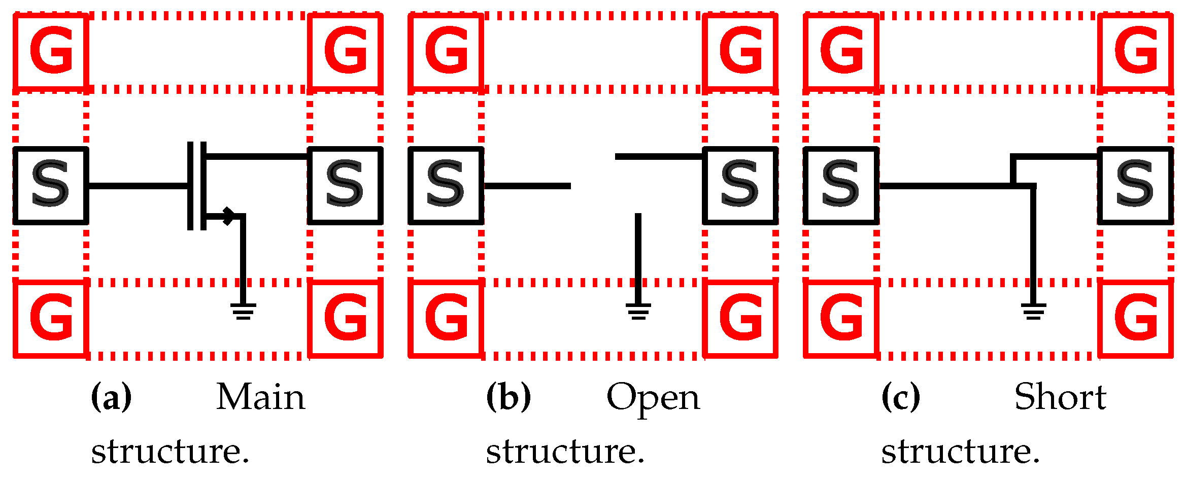
Figure 2.
Capacitor-like structures for Rg measurement.
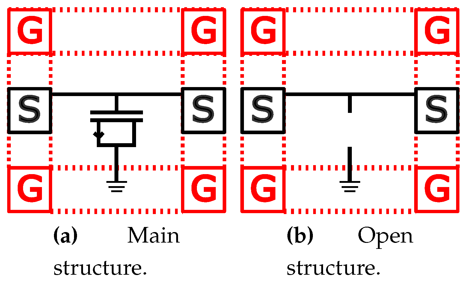
Figure 3.
Illustration of the gate resistance extraction methodology using the capacitor-like structure.
Figure 3.
Illustration of the gate resistance extraction methodology using the capacitor-like structure.
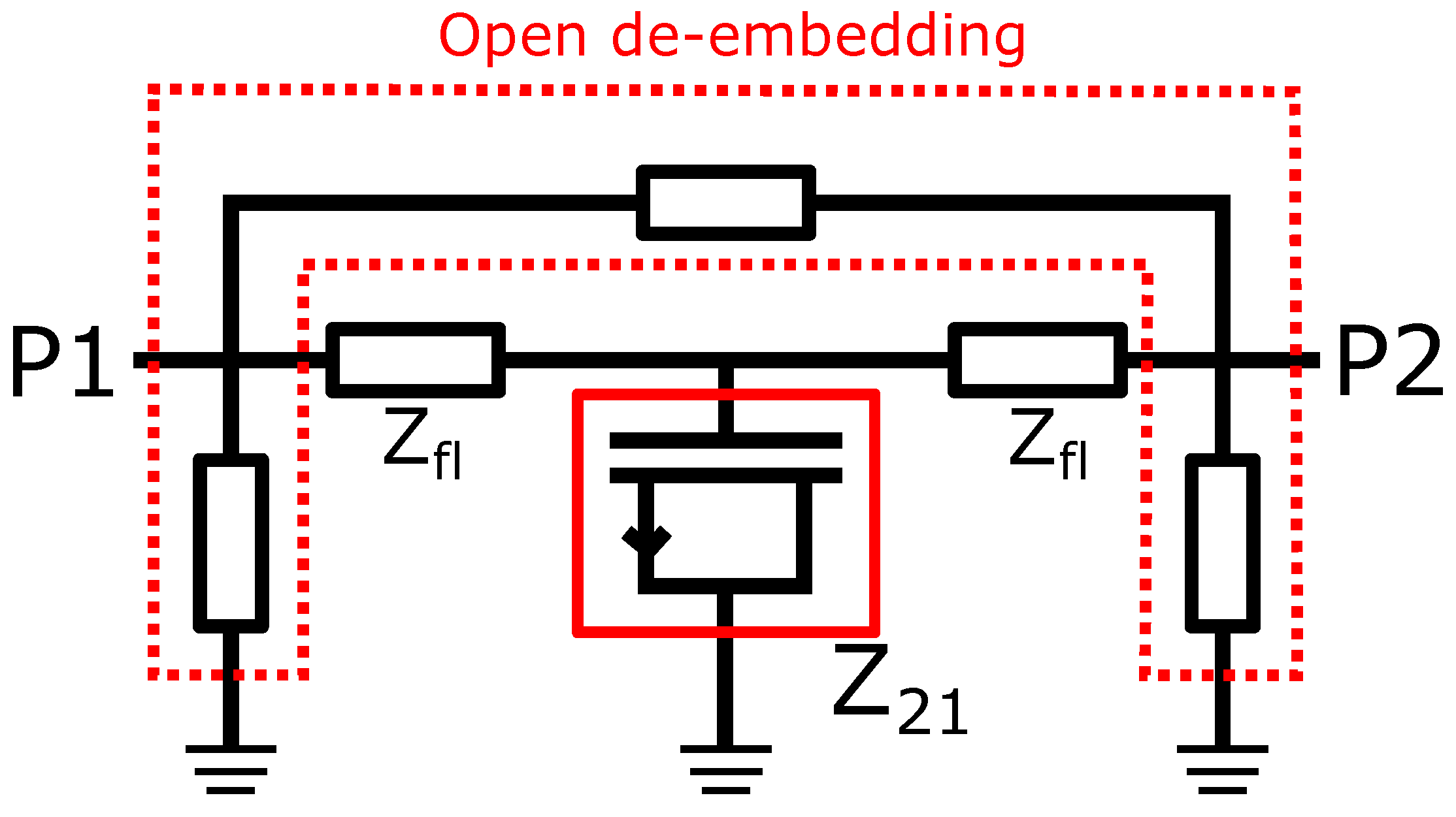
Figure 4.
Scaling behavior of gate resistance vs and M obtained from foundry model and from scaling law (eq.2 with , , ) with , at .
Figure 4.
Scaling behavior of gate resistance vs and M obtained from foundry model and from scaling law (eq.2 with , , ) with , at .
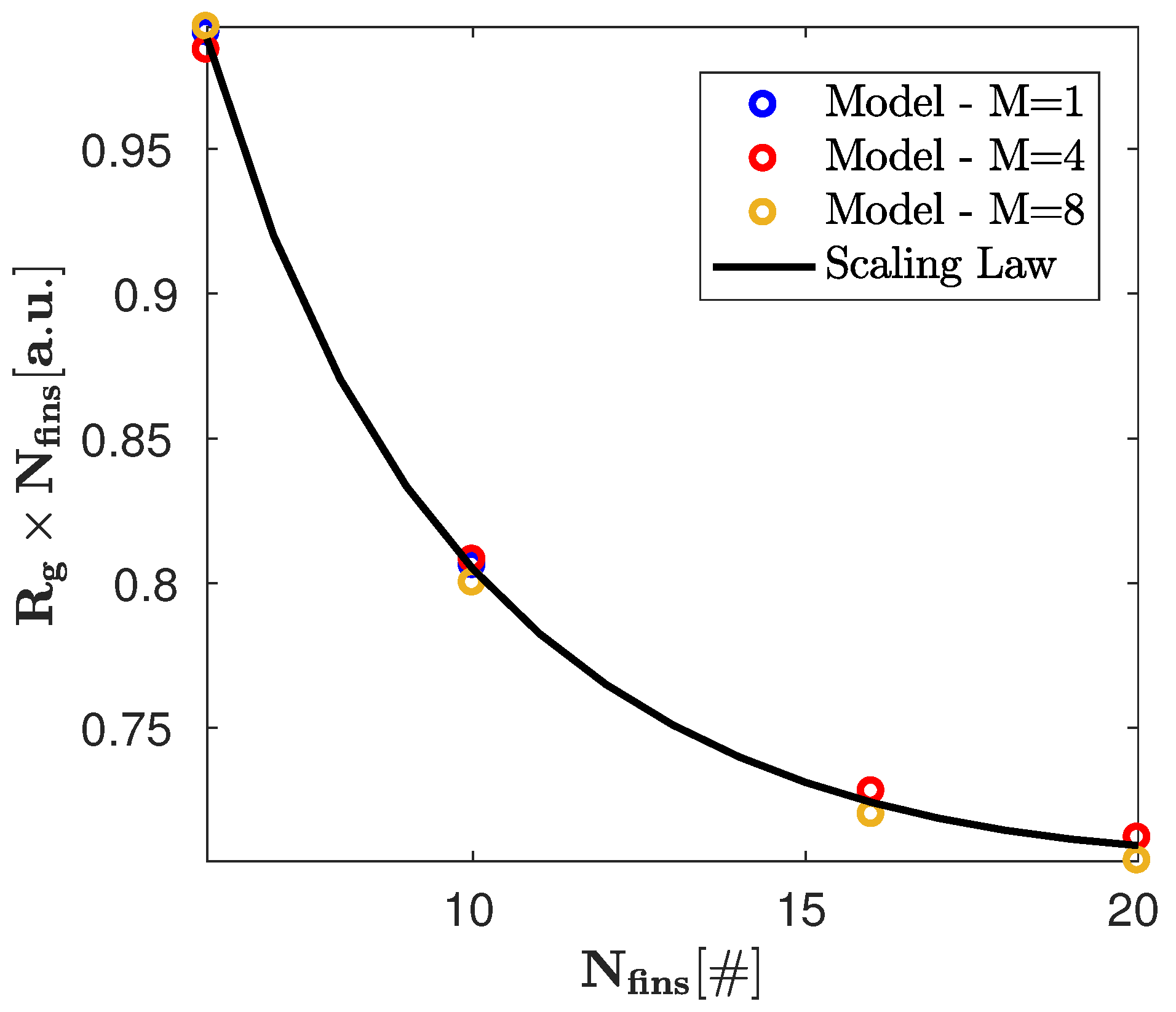
Figure 5.
Measured and simulated vs frequency on DUT12 for = .
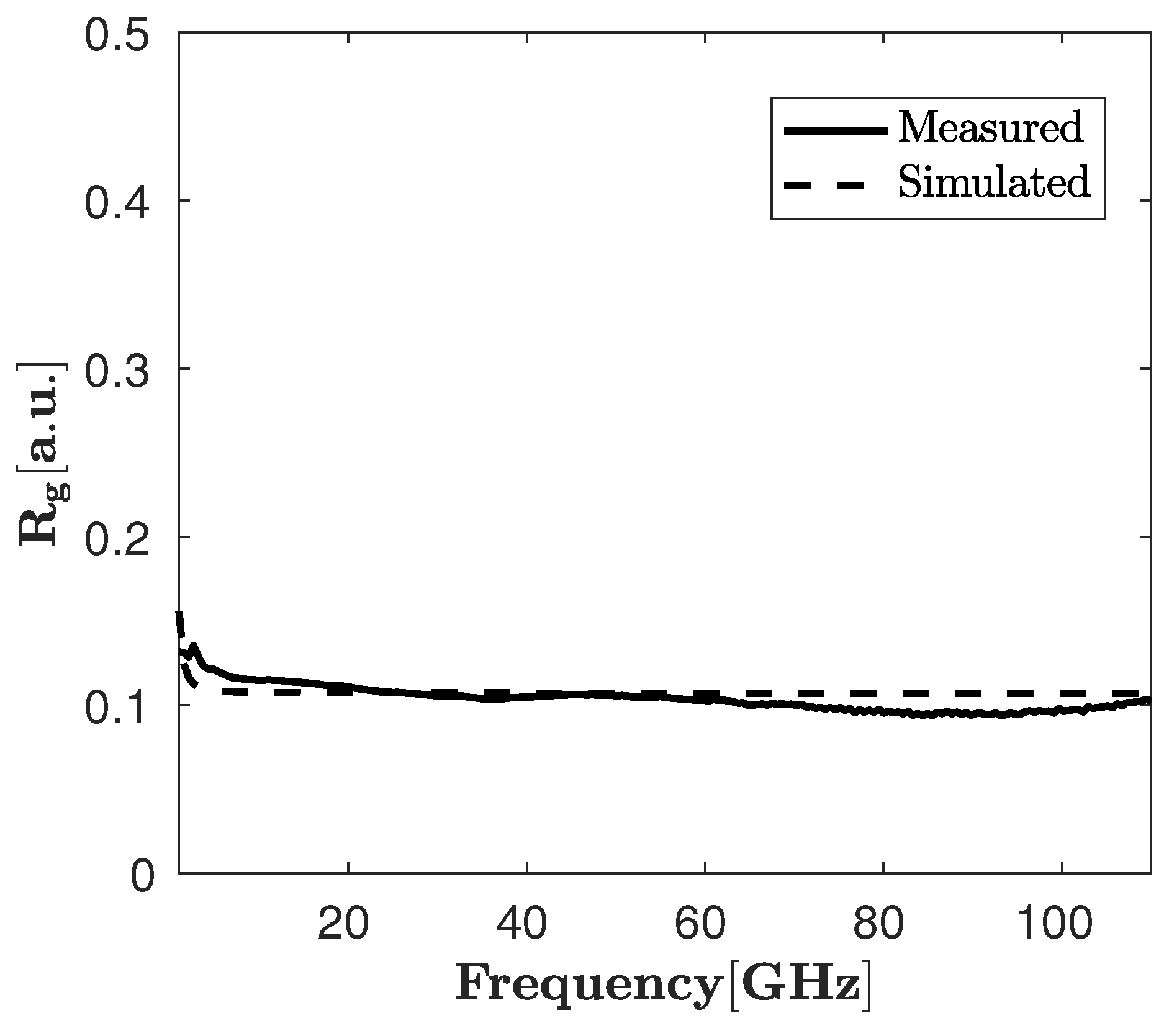
Figure 6.
Deviation of the measured gate resistance from simulation on DUT12 for different values of gate bias.
Figure 6.
Deviation of the measured gate resistance from simulation on DUT12 for different values of gate bias.

Figure 7.
Measured and simulated from capacitor-like structures with at = 50 and = as a function of and .
Figure 7.
Measured and simulated from capacitor-like structures with at = 50 and = as a function of and .
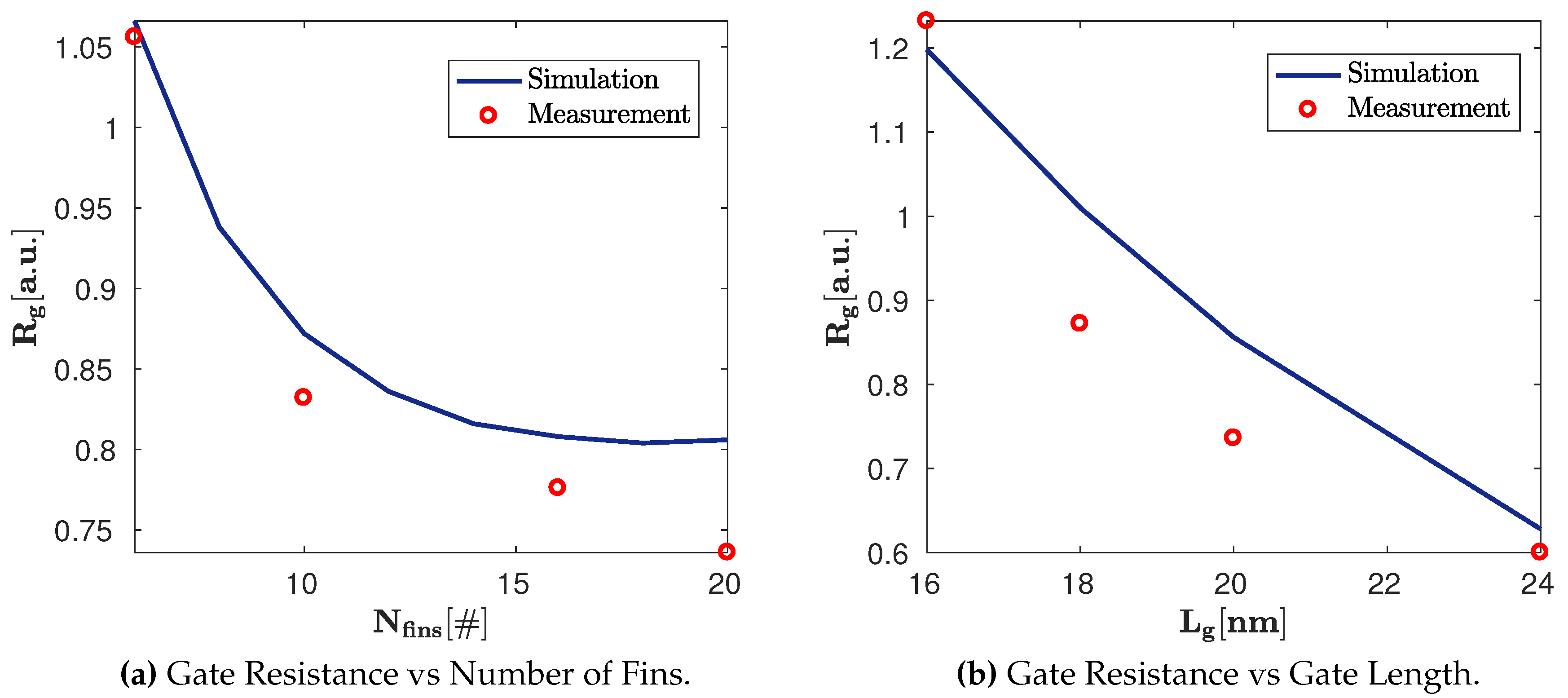
Figure 8.
Normalized variance of over frequency as a function of for standard (DUT16,17,18) and capacitor-like (DUT4,8,12) structures.
Figure 8.
Normalized variance of over frequency as a function of for standard (DUT16,17,18) and capacitor-like (DUT4,8,12) structures.
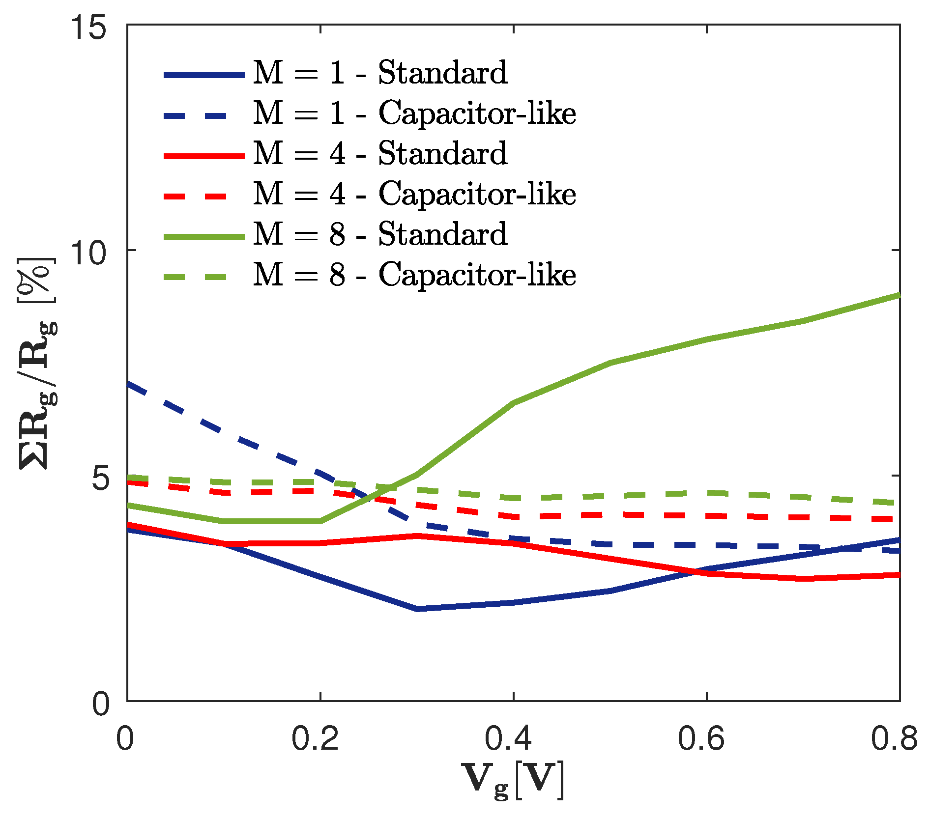

Table 1.
List of DUTs on the 16nm FinFET testchip.
| DUT | Structure Type | M | |||
|---|---|---|---|---|---|
| 1 | Capacitor-like | 6 | 10 | 20 | 1 |
| 2 | Capacitor-like | 10 | 10 | 20 | 1 |
| 3 | Capacitor-like | 16 | 10 | 20 | 1 |
| 4 | Capacitor-like | 20 | 10 | 20 | 1 |
| 5 | Capacitor-like | 6 | 10 | 20 | 4 |
| 6 | Capacitor-like | 10 | 10 | 20 | 4 |
| 7 | Capacitor-like | 16 | 10 | 20 | 4 |
| 8 | Capacitor-like | 20 | 10 | 20 | 4 |
| 9 | Capacitor-like | 6 | 10 | 20 | 8 |
| 10 | Capacitor-like | 10 | 10 | 20 | 8 |
| 11 | Capacitor-like | 16 | 10 | 20 | 8 |
| 12 | Capacitor-like | 20 | 10 | 20 | 8 |
| 13 | Capacitor-like | 20 | 10 | 16 | 8 |
| 14 | Capacitor-like | 20 | 10 | 18 | 8 |
| 15 | Capacitor-like | 20 | 10 | 24 | 8 |
| 16 | Standard | 20 | 10 | 20 | 1 |
| 17 | Standard | 20 | 10 | 20 | 4 |
| 18 | Standard | 20 | 10 | 20 | 8 |
Table 2.
in % at with for capacitor-like structures using transistors with various combinations of and M.
Table 2.
in % at with for capacitor-like structures using transistors with various combinations of and M.
| M | ||||
|---|---|---|---|---|
| 6 | 10 | 16 | 20 | |
| 1 | -52 | -18.3 | -5.6 | 3.9 |
| 4 | 9 | 3.8 | 4.2 | -1.6 |
| 8 | 1.7 | -1.8 | -4.2 | -1.7 |
Table 3.
in % at with for standard and capacitor-like structures with =20, =10, = 20 and different multiplicities.
Table 3.
in % at with for standard and capacitor-like structures with =20, =10, = 20 and different multiplicities.
| Structure Type | M | ||
|---|---|---|---|
| 1 | 4 | 8 | |
| Standard | 1.7 | 16.4 | 21 |
| Capacitor-like | 3.9 | -1.6 | -1.7 |
Disclaimer/Publisher’s Note: The statements, opinions and data contained in all publications are solely those of the individual author(s) and contributor(s) and not of MDPI and/or the editor(s). MDPI and/or the editor(s) disclaim responsibility for any injury to people or property resulting from any ideas, methods, instructions or products referred to in the content. |
© 2024 by the authors. Licensee MDPI, Basel, Switzerland. This article is an open access article distributed under the terms and conditions of the Creative Commons Attribution (CC BY) license (https://creativecommons.org/licenses/by/4.0/).
Copyright: This open access article is published under a Creative Commons CC BY 4.0 license, which permit the free download, distribution, and reuse, provided that the author and preprint are cited in any reuse.


