Submitted:
29 May 2023
Posted:
30 May 2023
You are already at the latest version
Abstract
In this work, the analytical Lagrange-Kirchhoff model for the deformation for a taiko plate silicon is proposed. Under the conditions of validity of the linear theory of thin plates, the model is in agreement with the experimental data.
Keywords:
Taiko wafer deformation
Introduction
Silicon wafers warp under residual
stress when they are thinned by grinding or plated with a thin layer of a
different material. Bifurcation and geometric instability of silicon wafers
occur at critical residual stresses that serve as the basis for evaluating the
significance of large deformations.
The magnitude of warpage strongly
depends on the thickness of the silicon substrate. Before the thinning process,
silicon wafers are generally thick enough to resist film stresses, and the
magnitude of warpage is small.
Unfortunately, the warpage
behavior of thin wafers is very different from that of thick ones. The first
one is the magnitude of warpage. The warpage can be so large that it shows
highly nonlinear behavior, or even bifurcation behavior, where the warped
shapes are asymmetric cylinders. Commercial equipment to measure small warpage
of bare wafers automatically compensates or minimizes gravitational effects
using a well-designed three-point support system. However, thinned wafers are
so flexible, and the warpage so great, that measurement with commercial
equipment is difficult. In large thin wafers the out of plane deflection can
exceed 8-10 times the wafer thickness.
Also, the corresponding dies
(chips) show a deformation but it is almost bifurcated. A thin die can be
bifurcated if the ratio between die deflection and die thickness is [3–10],
In real cases,
bifurcation is only possible for ultra-thin dies or if the residual stress is very high.
While, the 8”
thin wafers can have bifurcations even with not high deformations, the ratio
between wafer deflection and wafer thickness is [3–10],
For a t =
200 um thick wafer the bifurcation occurs with a deflection greater than 350
um.
1. Stresses and the Curvatures in a Linear Elastic Plate
Plate theory
is an approximate theory. It turns out to be an accurate theory provided the
plate is relatively thin but also that the deflections are small relative to
the thickness (deflection/t < 0.75) and when the ratio between the thickness t and
the plate width L is t/L <1/20. The plate showing the same elastic behavior in all
directions is called isotropic [1].
In case the plate
has different elastic properties in the two orthogonal directions is called
orthotropic. The elastic problem for an orthotopic plate, in the form developed
by Lagrange, is
Ex, Ey
Young's modules in x, y directions.
νij
(i, j = x, y)
is Poisson's ratio
of the substrate characterizing the compressive strain in the j direction
(direction of the effect) produced by the tensile stress in the i direction
(direction of the stress).
For the symmetry
conditions expressed by Green's relations, we also have
.
The Stresses
and the Curvatures in a Linear Elastic Plate are
for small
deflection,
Kx
and Ky are the curvatures in the x and y direction.
This important
assumption of small slope,
, means that the
theory to be developed will be valid when the deflections are small compared to
the overall dimensions of the plate.
In this work
we will analytically calculate the deflection and curvature of a silicon plate
and an annular silicon plate coated on one side with an aluminum layer with a
thickness of 4.5 um
2. The Moment-Curvature Equations
Consider a
plate subjected to bending moments Mx and My, with no other
loading (Plates subjected to Pure Bending without
twisting,
). From equilibrium considerations, these moments
act at all points within the plate they are constant throughout the plate. The
moment-curvature equations are un the set of coupled partial differential
equations,
The moment
curvature equations are analogous to the beam moment-deflection equation. The
factor Dx, Dy, is called the
plate stiffness or flexural rigidity and plays the same role in
the plate theory as does the flexural rigidity term E*I in the
beam theory.
Solving for the derivatives,
For a plate with axial symmetry (wafer), the relations 2.1, 2.2, 2.3 and 2.4 become
and
For an isotropic plate the equations are simplified,
The bending moment Mx and My induced by the layer are,
From equilibrium considerations, these moments act at all points within the plate – they are constant throughout the plate.
Equations 2.13 and 2.14 are combined to describe film stresses in terms of substrate curvatures:
where , are the corresponding intrinsic film stresses in the respective directions, in the other hand, material properties E and v correspond to those of substrate.
The relationships 2.18 and 2.19 are Stoney's formulas for isotropic coated rectangular substrate. Rearranging the relations (2.11) and (2.12),
Integrating the first two equations, the plate deflection can be written,
A = B = C = 0, if
Once the deflection w(x,y) is known, all other quantities in the plate can be evaluated.
For orthotropic plate, the deflection equations 2.17 is written,
and the curvatures are,
The relationships 2.22 and 2.23 are Stoney's formulas for orthotropic coated rectangular substrate.
If we assume a homogeneously deposited film, the stress in the two axes is isotropic and homogeneous (Circular Plate),
this for the general transformation rule and and
The equation 2.23 is Stoney' s formula for coated Circular Plate and the deflection w(r) is,
In the linear region, an increase in stress leads to a proportional increase in the curvature and a preservation of the spherical shape. Outside the linear region a further increase in stress, the shape rapidly transforms from spherical to cylindrical with a dominant curvature in a preferential direction. This phenomenon is called bifurcation of curvature. Figure 1 show a 720 µm thick wafer coated with a 4.5 µm thick AlCu layer.
We can calculate the residual stress of the thin film from warp measurements before and after AlCu layer deposition and from equation 2.23. The ΔCBow measurement is about 100 um (parabolic shape) and the residual stress is about 85 MPa (Silicon Young Modulus E = 131 GPa, ν=0.27, ts = 720 um, tf = 4.5 um) and the curvature is k= 0.024 1/m. The warpage have been measured with an MX-204 equipment (E+H Metrology).
Another way to obtain the same result eq. 2.23 is to solve the Equation of the Elastic Surface w(x,y) for circular plate supported and loaded with radial moment Mo at the outer edge is,
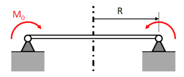
By integrating this equation 2.25 we obtain
, and are determined by the boundary conditions,
and
Constant moments (and tensions) across the plate. The bending moment induced by the coated layer is,
replacing in the (2.24) and (2.25),
we have found the equation (2.23).
3. Coated Circular plate with a Circular Hole at the Center
Let us Begin with a discussion of the bending of plate by the momentum Mi and Me uniformly distributed along the inner and outer boundaries, , and are determined by the equation (2.21) with the BC (1)
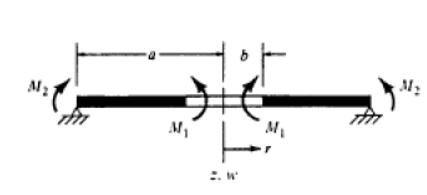
Form the equation 3.1 and BC, the annular plate deflection w(r) is,
the curvature are
The sum of substrate curvatures does not depend on r,
and in the case Re Ri
In particular cases,
a) Mi = Me = M0 the equation 3.2, 3.3 and 3.1 become
the deflection is
In this special case, for low defletion before di bifurcation, the annular plate and plate have the same curvature and deflection.
The bending moment M0 induced by the coated layer is
The equation 3.7 is the same as equation 2.27.
Figure 2.
Annular plate and plate have the same curvature and deflection.
b) Mi = 0, Me≠0
The deflection become,
and the curvature,
- Caso µ ≈ 1,
- Caso µ ≈ 0
In general, gaining a control on the warpage determined by the BSM residual stress can benefit the whole semiconductor industry and disclose future developments.
Moreover, it is known that with the increase of the size, the handling of a thinned wafer becomes more and more critical.
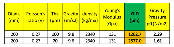
Another important aspect is the gravitational force (Gravity Induced Deflection (GID)). As the final thickness decreases, the wafer becomes progressively less able to support its weight,
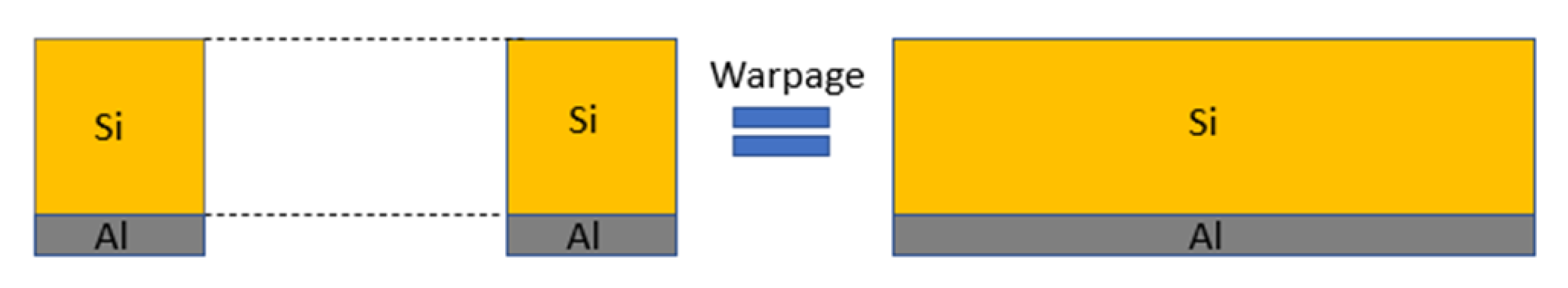
For this reason, in 2008 DISCO proposed the patented taiko process, which consists in a back-grinding method that leaves an annular region around the whole wafer. This solution, which is now a standard, allows an easier handling of the wafer itself and a reduction of the warpage. The unground edge ring of the thinned wafer greatly improves wafer strength and facilitates handling of the thin wafer,
This process method leaves a ring (approximately 3 mm) on the wafer outer edge and thin grinds only the inner area of the backside wafer. The taiko palate wafer can be considered as an annular plate bound to a circular plate. In case the thickness of the circular plate is much smaller than the thickness of the circular ring, we can neglect the effect of the constraint and calculate the taiko wafer deflection using the equation 3.7, with ts= 450 µm + tinner. On a 720 µm wafer we deposited a 4.5 µm thick layer of AlCu and performed the Taiko process after the taiko process the inner area has a thickness of 70 µm and the circular ring has a thickness of 450 µm (hr = 450 um, tinner= 70 µm and w = 3.7 mm). In Figure 3 a schematic drawing of the taiko plate is show.
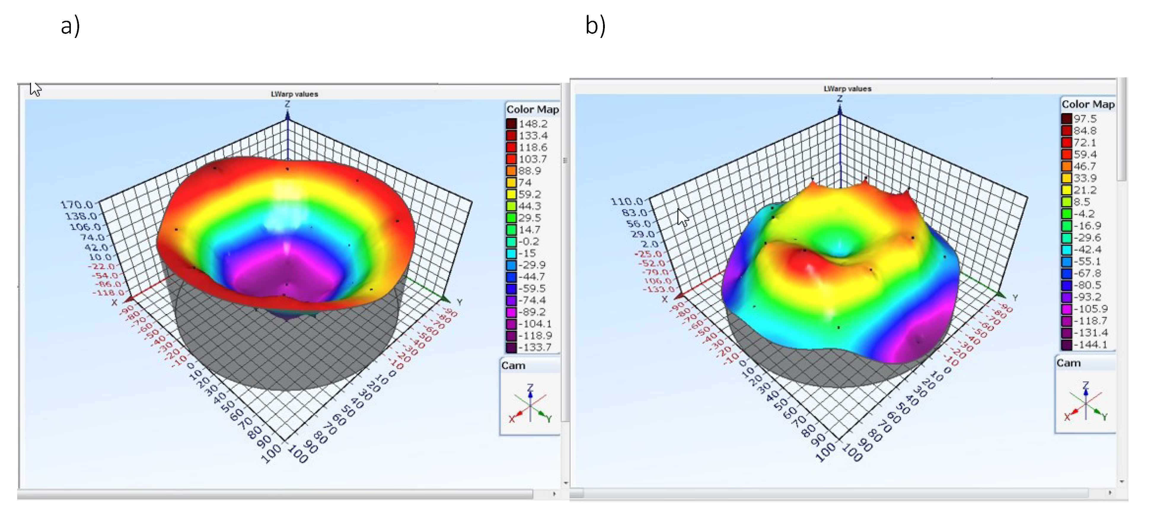
As we have previously shown the layer stress is 85 MPa. The deflection of a taiko wafer without AlCu layer and with AlCu layer are represented, Figure 4. The warpage have been measured with an MX-204 equipment (E+H Metrology). We using the equations 2.29, 3.9 and 3.7 we can verify that the taiko wafer warpage with a 4.5 AlCu with a residual stress of 85 MPa has about the same warpage value of a 520 um thick ring plate or circular plate (450 um+70 um) with the same layer. This result is valid if we are very far from the bifurcation condition [2,3,4,5,6,7,8,9,10].
Conclusion
The Lagrange-Kirchhoff model for the deformation for a taiko silicon plate silicon is proposed. Under the conditions of validity of the linear theory of thin plates, the model is in agreement with the experimental data. A predictive model of a taiko silicon plate deformation, under bifurcation conditions, will be the subject of future work.
References
- Timoshenko “Theory of Plates and Shells” MC GRAW HILL.
- V. Vinciguerra and A. Landi, "On the Way to understand the Warpage in 8' Taiko Semiconductor Wafers for Power Electronics Applications (Si and SiC)," in 2021 22nd International Conference on Thermal, Mechanical and Multi-Physics Simulation and Experiments in Microelectronics and Microsystems (EuroSimE), Virtual, 2021.
- H. Liu, J. Han, X. Tian, F. Dong, S. Chen and L. Lu, "Accurate determination of bifurcation points for ground silicon wafers considering anisotropy using FEM method," Materials Research Express, vol. 6, no. 9, 7 2019. [CrossRef]
- D. K. Shin and J. J. Lee, "Analysis of asymmetric warpage of thin wafers on flat plate considering bifurcation and gravitational force," IEEE Transactions on Components, Packaging and Manufacturing Technology, vol. 4, no. 2, pp. 248 - 258, Feb. 2014. [CrossRef]
- N. J. Salamon and C. B. Masters, "Bifurcation in isotropic thinfilm/substrate plates," International Journal of Solids and Structures, vol. 32, no. 3-4, pp. 473-481, Febbruary 1995. [CrossRef]
- C. B. Masters and N. J. Salamon, "Geometrically nonlinear stress-deflection relations for thin film/substrate systems with a finite element comparison," J. Appl. Mech., vol. 61, no. 4, pp. 872-878 (7 pages), Dec 1994. [CrossRef]
- L.B. Freund and S. Suresh, Thin Film Materials: Stress, Defect Formation and Surface Evolution, Cambridge: Cambridge University Press, 2004.
- L. B. Freund, "Substrate curvature due to thin film mismatch strain in the nonlinear deformation range," Journal of the Mechanics and Physics of Solids, vol. 48, no. 6, pp. 1159-1174, 2000. [CrossRef]
- V. Vinciguerra, G. L. Malgioglio and A. Landi, "Modelling the Elastic Energy of a Bifurcated Wafer: A benchmark of the Analytical Solutions vs. the ANSYS Finite Element Analysis," Composite Structures, 114996, vol. 281, 2022.
- L. B. Freund, J. A. Flora and E. Chason, "Extensions of the Stoney formula for substrate curvature to configurations with thin substrates or large deformations," Applied Physics Letters, vol. 74, no. 14, p. 1987, 1999. [CrossRef]
Figure 1.
Warp measurement post deposition AlCu@4.5um layer, t = 720 um.
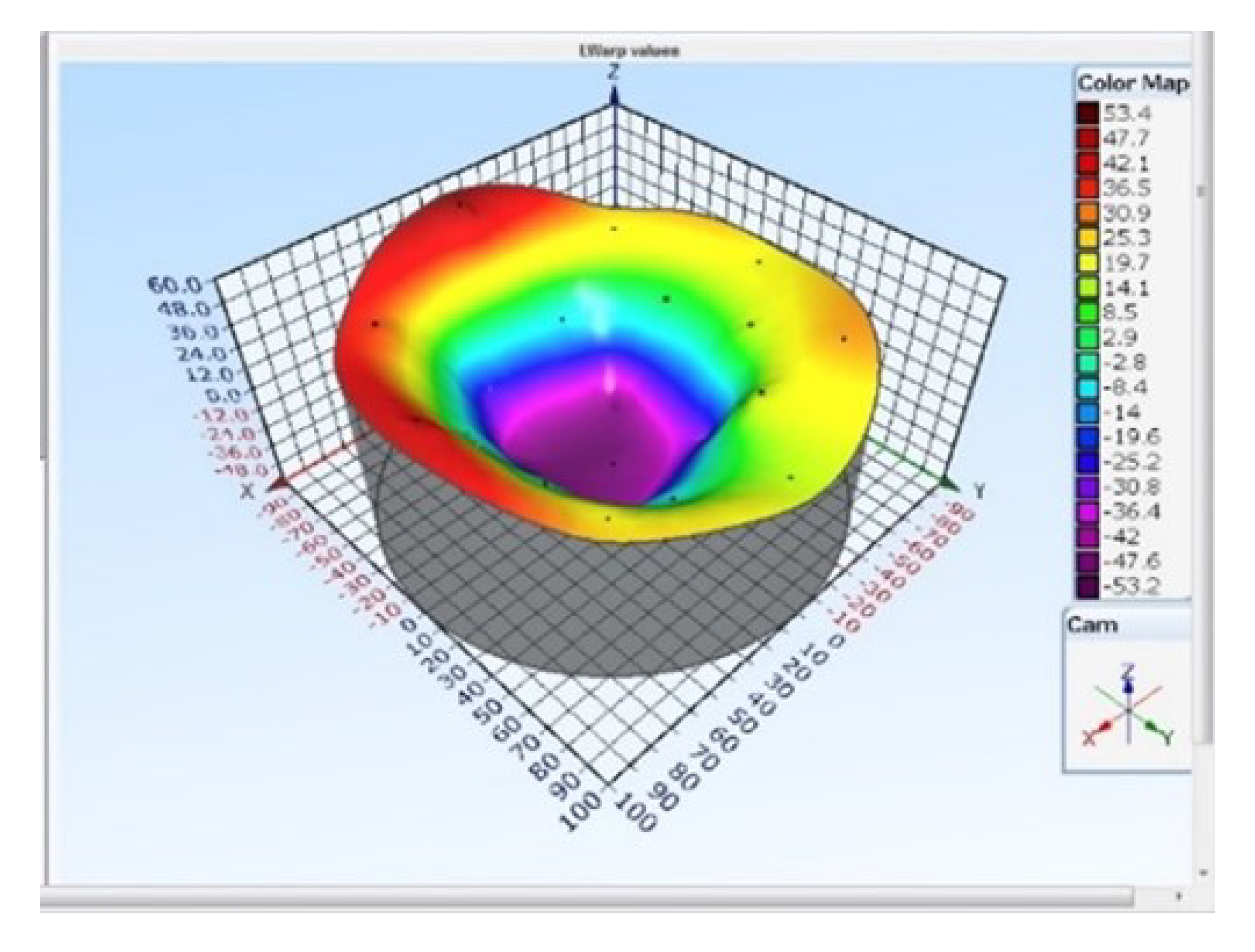
Figure 3.
Annular plate (a) and taiko plate (b).
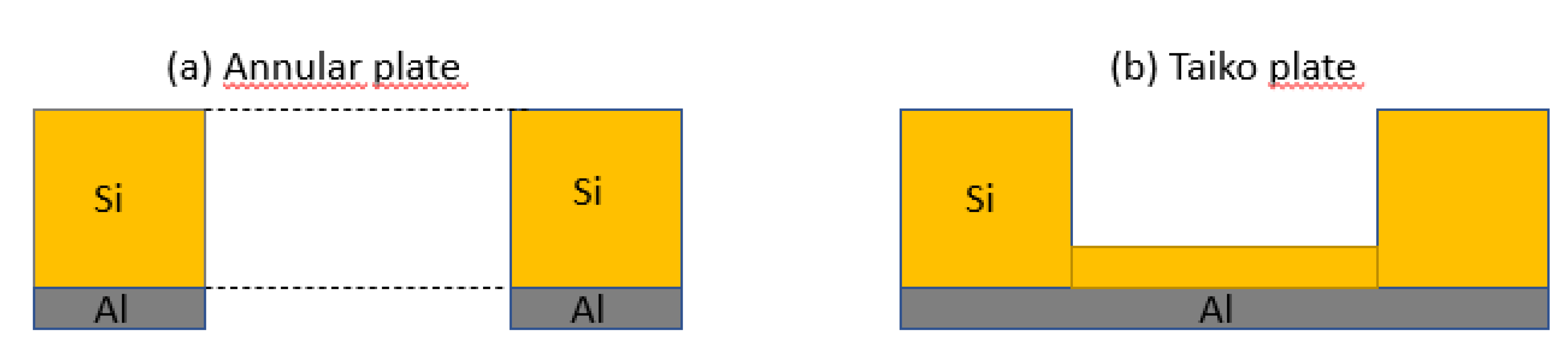
Figure 4.
Taiko@70 µm, without AlCu a), Center Bow = 210 (ring up measurements) um and with AlCu layer 4,5 µm on front side b) (ring up measurements), Center bow = -3 um , ΔCbow = 213 µm.
Figure 4.
Taiko@70 µm, without AlCu a), Center Bow = 210 (ring up measurements) um and with AlCu layer 4,5 µm on front side b) (ring up measurements), Center bow = -3 um , ΔCbow = 213 µm.
Disclaimer/Publisher’s Note: The statements, opinions and data contained in all publications are solely those of the individual author(s) and contributor(s) and not of MDPI and/or the editor(s). MDPI and/or the editor(s) disclaim responsibility for any injury to people or property resulting from any ideas, methods, instructions or products referred to in the content. |
© 2023 by the authors. Licensee MDPI, Basel, Switzerland. This article is an open access article distributed under the terms and conditions of the Creative Commons Attribution (CC BY) license (http://creativecommons.org/licenses/by/4.0/).
Copyright: This open access article is published under a Creative Commons CC BY 4.0 license, which permit the free download, distribution, and reuse, provided that the author and preprint are cited in any reuse.


