Submitted:
26 May 2023
Posted:
30 May 2023
You are already at the latest version
Abstract
This study aims to theoretically address the design and analysis of an efficient pressure sensor designed by using a polymer-based defective 1D annular photonic crystal (APC). The 1D APC comprises an alternate arrangement of Si and SiO2 in a cylindrical fashion, incorporating a central defect layer. The investigation of the reflectance characteristics of the proposed structure is conducted by separately considering the polystyrene (PS) and the polymethyl methacrylate (PMMA) polymer materials as the defect layer. The pressure-sensitive refractive index of the polymers and the constituent materials of the APC plays a vital role in envisaging the pressure-sensing application. The cornerstone of this study is represented by the shift analysis in the wavelength of the defect mode inside the band gap using different applied pressures by employing the modified transfer matrix method (MTMM). Various geometrical parameters like the defect polymer layer’s thickness and the APC period were carefully optimized to achieve higher sensing performance. The proposed design demonstrated a remarkable pressure sensitivity and FoM of 51.29 nm/GPa and 301.7 GPa-1, respectively, which is considerably high in the current research scenario. It is believed that the proposed structure can be an apt candidate as an innovative high-performance pressure sensor, and it can play a key role in photonic integrated circuits.
Keywords:
Annular photonic crystal
; polymer material
; transfer matrix method
; pressure sensor
; sensitivity
1. Introduction
Photonic crystal (PhC) is a brand-new class of optical material, which comprises a periodic arrangement of dielectric constant and can be realized in 1D, 2D, and 3D configurations [1,2,3]. In the last decade, 1D PhC attracted much attention within the scientific community because of its unique capability of controlling the flow of electromagnetic waves inside the crystal. The trapping of light inside the PhC structure is governed by the photonic bandgap (PBG) effect, where a particular spectral band is prohibited to propagate through the structure [4]. Remarkably, by inserting a defect layer in such a structure, its periodicity breaks, leading to the formation of strongly localized allowed states inside the PBG [5]. The PBG acts as a reflection band and, therefore, the defect mode appears to be a sharp passband in the PBG. The characteristics of the defect mode can be controlled by changing the defect layer’s refractive index and thickness. This tunable property of the defect mode makes the defect-based 1D PhC the most researched topic due to its broad-ranging application domains like sensing, filtering, waveguiding, agriculture, food safety, and bio-medical applications [6,7,8,9].
With the ongoing remarkable advancements in nanotechnology, it is feasible to fabricate various geometrical configurations of PhC [10,11,12]. Recently, a new configuration of 1D PhC known as 1D cylindrical multilayer structure has fascinated a lot of researchers worldwide due to its remarkable performance, particularly in sensing and filtering applications [13,14,15]. The cylindrical PhC is referred to as an annular photonic crystal (APC) or circular photonic crystal (CPC). The APC structure can be constructed by arranging alternative layers of different materials in a cylindrical ring fashion [16]. The flow of EM waves in APC was first investigated by M.A. Kaliteevkki and his team in 1999. After that, C.A. Hu et al. proposed a modified transfer matrix method (TMM) using cartesian coordinates for the analysis of transmittance and reflection characteristics of the APC [17]. Additionally, the authors thoroughly explained the fabrication feasibility of APC structure and studied the liquid sensing application. Furthermore, J. Scheuer et al. [18] introduced a ring defect into the APC structure to make annular Bragg lasers. Moreover, a wide variety of materials, such as metal, dielectric, superconductor, metamaterial, etc. can be used to develop APC structures [19,20,21]. Recently, APC structures have been extensively studied for sensing applications. For example, M.M. Abadla et al. theoretically demonstrated a temperature sensor using 1D APC, where the authors studied the shift in the transmittance characteristics of the structure with a temperature rise. They achieved a significant temperature sensitivity of 0.033 nm/oC [22]. S.K. Srivastava et al. designed a 1D ternary annular PhC, where a unit cell consists of a semiconductor, superconductor, and air. The authors investigated the reflectance spectrum for both the TE and TM modes by changing the starting radius and temperature [23]. A defect-based 1D APC with a configuration of (Si/SiO2)N/2 (TiO2) (Si/SiO2)N/2 is proposed in [24]. With the help of TMM, the authors studied the transmission spectrum to analyze the shift in the defect mode frequency for varying temperatures across the defect layer. In the same vein, A. Mehany et al. designed a porous silicon-based multilayer 1D APC, where different layers contain a different percentage of porosity. The authors studied the shifting nature of the Tamm resonance mode by varying the analyte refractive index from 1 to 1.5 and accomplished a remarkable sensitivity of 6770 nm/RIU [25]. S.K. Srivastava et al. designed a 1D APC by using double negative metamaterials and studied its reflectance spectrum at different azimuthal mode numbers [26]. Similarly, S. Gandhi et al. reported a porous Si-based annular 1D PhC to detect the creatinine concentrations in blood, where they observed a maximum sensitivity of 640.29 nm/RIU and a quality factor in the order of 105. S. Jena et al. demonstrated a hydrostatic pressure sensor using different configurations of regular plannar 1D PhC [27]. In addition, F. Segovia et al. [28] and A. Herrera et al. [29] studied the shifting nature of the defect mode and band gap in relation to a rising hydrostatic pressure by using plannar 1D PhC. In another related study, Liu et al. carried out an experimental investigation on the dual-core photonic crystal fiber for pressure sensing from 0 MPa to 45 MPa [30]. The regulation and detection of such high pressure are quite difficult, which imposes a great challenge in the experimental realization of the device. Although the pressure sensing application has been explored by using plannar 1D PhC and photonic crystal fiber, there is still plenty of improvement potential for sensing performance by investigating the effect of pressure using the APC.
Various materials can be used for creating different layers and defect layers of the PhC. These materials can be semiconductors, dielecctrics, metals, superconductors, metamaterials, etc. Recently, polymer materials have emerged as a potential candidate for designing 1D PhC owing to their exceptional tunable optical properties. By stretching and compressing the polymer materials [31,32], it is convenient to modify their properties, which is beneficial in numerous applications, such as sensors, filters, reflectors, etc. [33,34].
This study is significant research as it provides a couple of novelties in the current research scenario. A thorough analysis of a novel polymer-based 1D APC is provided in the study to be used in the pressure sensing application field. The primary benefit of using a polymer material is that it shows an elasto-optic effect so that the optical properties can be easily modified by applying external pressure. The mainstay of this research is to study the tunable characteristics of the defect mode with pressure variations. Moreover, a complete optimization of different geometrical parameters has been performed to achieve a remarkable sensing performance. Additionally, a 3D plot of the reflectance spectrum is studied to enhance the novelty of this study. It is believed that this work can be a torchbearer in the pressure-sensing application field.
2. Proposed Structure and Mathematical Modelling
The cross-sectional view of the proposed binary defect-based APC is illustrated in Figure 1. The design comprises an inner-most circular region (a starting section), which has a refractive index (RI) of and radius of . Also, alternating layers of Si and SiO2 are deposited, whose RI is and , respectively, and the radius is and , respectively. A defect layer of RI and radius is inserted in the proposed APC to realize a defect mode in the transmittance spectrum. The period of APC before and after the defect layer is , where N denotes the total period of the structure. Here, the value of N is taken as 10. The entire configuration of the designed structure is . In this study, the proposed structure is analyzed by considering the defect layer as polymer materials like PS and PMMA. The outer region (the final medium) is the substrate layer, which has RI and radius .
It is assumed that the cylindrical waves emerged from the core and diverged further toward the higher layers. In the cylindrical coordinates, the Helmholtz wave equations are used to mathematically explain the E-type mode (Ez, Hϕ, H), which can be written as follows [35,36]:
By stating as , and readjusting, we can write [37],
where and denote the 1st and 2nd order of the Bessel’s function, respectively. The symbol q represents the propagation constant, which is expressed as . The tangential component is stated as follows:
To simplify the calculation, we consider only the fundamental mode (i.e., v=0), so the simplified field equations are written as follows:
The fields can be represented in a matrix form as follows [22]:
where The amplitude factors A and B can be expressed as,
By an equivalent field at is given as:
As the amplitude remains the same within a particular layer, we can write,
By putting eq. 9 in eq. 8, we get,
where is the transfer matrix. Upon simplifying , we can get the following equations:
By performing a similar type of analysis for other layers, the electric field at the 1st layer and the Nth layer can be related as,
where the symbol M denotes the overall transfer matrix, which can be obtained by multiplying the transfer matrix of the individual layers.
2.1 Pressure-Dependent Refractive Index of Constituent Materials
The photoelasticity effect is the method, which is utilized to investigate the sensor’s pressure, where the material’s refractive index (RI) differs in accordance with different stress/pressure values. Specifically, the stress is associated with field components through the photoelastic constant as the fourth power of the refractive index. This variation in the RI of the material for different pressure values can be studied by using a photoelastic constant. By using the photo-elasticity effect, the dependence of the refractive index on the stress effect can be expressed as follows [38]:
where represents the strain-optic coefficient, n denotes the RI, and represents the stress component. For an isotropic medium, the pressure-dependent RI can be written as [39]:
where is the material’s RI, which corresponds to zero applied pressure, and can be specified as follows:
where and signify the strain-optic coefficients, represents the Poisson’s ratio and E denotes the Young’s modulus. According to the proposed structure, the values of different constants for the materials Si, SiO2, PS, and PMMA are obtained from [40,41].
3. Results and Discussion
The suggested 1D APC is designed by using the successive layers of Si and SiO2 with a period N=10, where a defect layer is introduced in the middle of the APC. The structure is analyzed by separately considering the polymer materials (i.e., PS and PMMA) as the defect layer. Therefore, the proposed two different configurations are and . The thickness of the Si and SiO2 layer is taken as and , respectively, whereas the thickness of the starting medium is . It is observed that the thickness of the starting medium () is considerably larger compared to the thickness of the constituent layers () of the APC. A greater value of confirmed that the designed APC analogously acts to the plannar 1D PhC. Initially, the thickness of the defect layer is considered as , and the period (N) is taken as 10. As considered, light incidents normally onto the structure, and the azimuthal number (m) is assumed to be zero in order to avoid the computational complexity. The modified transfer matrix method (TMM) is employed to study the reflectance spectrum of the proposed APC. The polymer materials (PMMA and PS) are comparatively less rigid than the traditional semiconductor materials like Si and SiO2. Therefore, they possess highly tunable RI characteristics concerning pressure change.
To begin with, the reflectance spectrum of the structure is studied by separately considering the defect layer as PS and PMMA, which is shown in Figure 2. It can be observed that a band gap is obtained from 1145 nm to 2071 nm in the reflectance. Remarkably, a sharp dip (i.e., a defect mode) within the band gap is perceived at 1475 nm and 1450 mm for the PS and PMMA as the defect layer or layers, respectively. The mainstay of this study is to investigate the defect mode’s characteristics concerning various applied pressures across the defect layer.
Next, the pressure-sensing application of the proposed APC has been analyzed by selecting PS as the defect medium. Figure 3 demonstrates the shift in the defect mode inside the band gap by increasing the pressure across the defect layer from 0 GPa to 3 GPa. It is observed that with changes in the pressure, the band gap range remains fixed, whereas the defect mode position undergoes a noticeable shift. In particular, the position (wavelength) of the defect mode is blue-shifted from 1475 nm to 1427 nm to 1382 nm to 1341 nm as the pressure increases from 0 GPa to 1 GPa to 2 GPa to 3 GPa, respectively. Also, it is observed that the intensity of the defect mode decreases with an increase in the applied pressure.
After that, a shift in the position of the defect mode occurred with different applied pressures by considering PMMA as the defect layer. As depicted in Figure 4, the wavelength of the defect mode is moved from 1450 nm to 1414 nm to 1379 nm to 1348 nm, as the pressure increases from 0 GPa to 1 GPa to 2 GPa to 3 GPa, respectively. The primary reason for such a shift (as shown in Figure 3 and Figure 4) in the defect mode position is that the RI of the PS and PMMA layer changes with a change in pressure, which modifies the overall transfer matrix, and results in a definite shift in the wavelength of the defect mode. This phenomenon can be well explained by the following mathematical equation:
where and denote the optical and geometrical path difference, respectively. represents the wavelength, is the effective refractive index, and m is an integer. When the pressure across the defect layer increases, the value of increases, thereby making the shift toward a higher value in order to keep fixed.
The variation in the position of the defect mode is plotted in relation to changes in the pressure parameter, as shown in Figure 5. It is observed that for the PS and PMMA together as a defect layer, the defect mode wavelength decreases almost linearly with an increase in pressure. For a low pressure (0-2 MPa), the PS-based APC, the defect mode position or positions took place at relatively a higher wavelength compared to the PMMA-based APC. By contrast, for high pressure (i.e., 3 MPa), the PS-based APC showed a higher defect mode wavelength than the PMMA-based APC. The fitting equation for the variation of the defect peak position for constant changes in pressure can be mathematically represented as follows:
where is in and is in .
The variation in the intensity of the defect mode peak is investigated with changes in pressure, as shown in Figure 6. A lower intensity value of the defect mode indicated accurate detection of the defect mode’s position. As shown in the figure, for both the PS and PMMA-based APC, the intensity decreases with a rise in the applied pressure. In particular, the intensity decreases from 0.1699 to 0.104 to 0.0402 to 0.0038 for the PS-based APC and 0.1305 to 0.0825 to 0.0374 to 0.0081 for PMMA-based APC, as the pressure increases from 0 GPa to 1 GPa to 2 GPa to 3 GPa, respectively.
After that, the sensor’s sensitivity, which is the most significant parameter to assess the sensor’s performance, is calculated. The sensitivity is measured by the geometrical parameters at , , and N=10. As depicted in Figure 7, the sensitivity of the sensor decreases with a rise in pressure. For the PS-based APC configuration, a maximum sensitivity of 49.31 nm/GPa has been achieved at =0 GPa, whereas for the PMMA-based APC structure, a maximum sensitivity of 36.73 nm/GPa is obtained at =0 GPa. Accordingly, such a significant sensitivity of the proposed structure can make it a robust candidate in the pressure sensing application field. In addition to the pressure sensitivity, other important sensing parameters, such as quality factor, FWHM, and figure of merit for both the PS defect-based APC and the PMMA defect-based APC, were also computed, as illustrated in Table 1 and Table 2, respectively.
To provide a deeper understanding of the shifting nature of the defect mode, a 3D plot of the reflectance has been examined for the pressure and wavelength. Figure 8 and Figure 9 represent the reflectance spectrum concerning pressure variation for PS defect and PMMA defect-based APC, respectively. As illustrated, the blue color line indicates the lower and upper edge of the band gap. It can be observed that the defect mode appeared within the band gap, and the wavelength of this defect mode continued to decrease with an increase in the applied pressure. This nature of variation is exactly similar to the variation explained in Fg.5.
To optimize the thickness of the defect layer (), the sensitivity and FoM were computed by changing the value of from 180 nm to 260 nm, and at a fixed , , and N=10. It is observed that for 260 nm<<180 nm, both the defect mode intensity and full-width half maximum (FWHM) are high, leading to the realization of low sensing parameters. Thus, is considered within the range of 180 nm and 260 nm only. For each value of , the sensitivity and FoM were measured for the applied pressure within the range of 0 GPa and 3 GPa. As shown in Figure 10, it is observed that with an increase in thickness, sensitivity increases for both PS and PMMA defect-based APC structures. A maximum sensitivity of 51.29 nm/GPa and 38.92 nm/GPa is obtained for the PS and PMMA defect-based APC configuration, respectively. As shown in Figure 11, it is obvious that FoM increases with an increase in . It is also observed that the PS defect-based APC achieved a higher FoM versus the PMMA defect-based APC structure. A maximum FoM of 326.2 1/GPa and 250.6 1/GPa is accomplished for the PS and PMMA defect-based APC configuration, respectively. Based on the above discussion of results, it is confirmed that an optimum sensitivity and FoM are obtained at . Thus, the optimized value of is obtained as 260 nm.
Subsequently, the effect of the number of periods of APC on sensitivity and FoM is studied, as illustrated in Figure 12 and Figure 13, respectively. This simulation is carried out by setting and , , and changing the period (N) from 8 to 12. As shown in Figure 12, there is very little variation in sensitivity with an increase in the value of N. For the PS defect-based APC, the sensitivity is significantly higher compared to the PMMA defect-based APC. On the other hand, the value of N has a substantial impact on the FoM. As depicted in Figure 13, the FoM increases with an increase in the value of N. Like sensitivity, the PS defect-based APC obtained superior FoM compared to the PMMA defect-based APC. Consequently, sensitivity is the most significant sensing parameter, and it remains almost unaffected by changes in the value of N. Thus, the optimized value of N is obtained as 10.
4. Conclusions
In this study, a novel polymer defect-based 1D annular photonic crystal sensor is designed and examined. The proposed sensor is effectively capable of sensing pressure from 0 MPa to 3 MPa. The designed structure comprises alternate layers of Si and SiO2. This structure is studied by separately considering two polymer defect layers (i.e., PS and PMMA). The modified transfer matrix method is employed to examine the reflectance characteristics of the proposed structure. The sensing principle is based on the tuning of the defect mode wavelength inside the band gap of the reflection spectra with different applied pressures. A 3D plot of the reflectance spectrum of the proposed APC is studied with pressure variation. Under the case of normal incidence, and at optimized structure parameters of and , , and N=10, the proposed PS defect-based APC provided a maximum sensitivity and FoM of 51.29 nm/GPa and 301.7 GPa-1, respectively. On the other hand, the PMMA defect-based APC provided a maximum sensitivity and FoM of 38.92 nm/GPa and 231.7 GPa-1, respectively. Therefore, it is concluded that for the designed structure, PMMA as a polymer material outperformed compared to PS polymer in the pressure sensing application. The fabrication’s feasibility and stability of the reflectance characteristics of the proposed structure made the designed structure in this study a suitable candidate for the pressure sensing application.
Author Contributions
Project administration, A.A. A., A. P., H.A.E., and A. M.; Supervision, A.H.M.A., G.A.A., H.A.E., and A. M.; Software, A.A. A.; Visualization, H.A.E., A.A. A.; Writing—review & editing, H.A.E., G.A.A., A.H.M.A., and A. M.; Writing—original draft, A. P., and D. D. P; Methodology, H.A.E., and A.A. A.; Data curation, A.A. A., A. M., and H.A.E.; All authors have read and agreed to the published version of the manuscript.
Funding
The authors are thankful to the Deanship of Scientific Research at Najran University for funding this work under the Research Groups Funding program grant code (NU/RG/SERC/12/2).
Availability of data and material
Requests should be addressed to corresponding author.
Conflicts of Interest
The authors declare no conflict of interest.
References
- A Panda, PD Pukhrambam, Design and analysis of porous core photonic crystal fiber based ethylene glycol sensor operated at infrared wavelengths, Journal of computational electronics, vol. 20, pp. 943-957, (2021).
- Tao Li et al., Recent advances in photonic crystal-based sensors, Coordination Chemistry Reviews, vol. 475, p. 214909, (2023). [CrossRef]
- A Panda, P.D. Pukhrambam, J.W. Simatupang, Design of a Highly Sensitive Self-Reference Tamm-Plasmon-Polariton Sensor Employing Ti3C2Tx MXene, IEEE Sensors Journal, vol. 22 (13), pp. 12719-12727, (2022). [CrossRef]
- Arafa H. Aly, Fatma A. Sayed, Hussein A. Elsayed, “Defect mode tunability based on the electro-optical characteristics of the one-dimensional graphene photonic crystals,” Applied optics, vol. 59, no. 16, pp. 4796-4805, (2020). [CrossRef]
- A.H. Aly et al., Theoretical study of hybrid multifunctional one-dimensional photonic crystal as a flexible blood sugar sensor, Physica Scripta, vol. 95, no. 3, p. 035510, (2020). [CrossRef]
- Giuseppe Maria Paterno et al., Hybrid One-Dimensional Plasmonic−Photonic Crystals for Optical Detection of Bacterial Contaminants, Journal of Physical Chemistry Letters, vol. 10, no. 17, pp. 4980-4986, (2019). [CrossRef]
- N.R. Ramanujam et al., Numerical characterization of 1D-Photonic crystal waveguide for female reproductive hormones sensing applications, Physica B: Condensed Matter, vol. 639, p. 414011, (2022). [CrossRef]
- Jihene Zaghdoudi, Mounir Kanzari, One-dimensional photonic crystal filter using a gradient-index layer, Optik, vol. 160, pp. 189-196, (2018). [CrossRef]
- Watcharakitchakorn, R. Silapunt, Design and Modeling of the Photonic Crystal Waveguide Structure for Heat-Assisted Magnetic Recording, Advances in Materials Science and Engineering, vol. 2018, p. 8097841, (2018). [CrossRef]
- D. Devashish, O.S. Ojambati, S.B. Hasan, J.J.W. van der Vegt, W.L. Vos, Three dimensional photonic band gap cavity with finite support: enhanced energy density and optical absorption, Phys. Rev. B, vol. 99, p. 075112, (2019). [CrossRef]
- N. Liu, H. Guo, L. Fu, S. Kaiser, H. Schweizer, H. Giessen, Three-dimensional photonic metamaterials at optical frequencies, Nat. Mater., vol. 7, no. 1, pp. 31–37, (2007). [CrossRef]
- S. Yang, Y. Zhang, X. Peng, Y. Lu, S. Xie, J. Li, W. Chen, Z. Jiang, J. Peng, H. Li, Theoretical study and experimental fabrication of high negative dispersion photonic crystal fiber with large area mode field, Optic Express, vol. 14, no. 7, p. 305, (2006). [CrossRef]
- M.S. Chen, C.J. Wu, T.J. Yang, Optical properties of a superconducting annular periodic multilayer structure, Solid State Commun., vol. 149, pp. 1888–1893, (2009). [CrossRef]
- Y.A. Urzhumov, D.R. Smith, Transformation optics with photonic band gap media, Phys. Rev. Lett. 105 (16) (2010). [CrossRef]
- T. Erdogan, O. King, G.W. Wicks, D.G. Hall, E.H. Anderson, M.J. Rooks, Circularly symmetric operation of a concentric circle grating, surface emitting, AlGaAs/GaAs quantum well semiconductor laser, Appl. Phys. Lett., vol. 60, no. 16, vol. 1921–1923, (1992).
- S.K. Srivastava, A. Aghajamali, Investigation of reflectance properties in 1D ternary annular photonic crystal containing semiconductor and high-T c superconductor, J. Supercond. Nov. Magnetism, vol. 29, no. 6, pp. 1423–1431, (2016). [CrossRef]
- M.A. Kaliteevski, R.A. Abram, V.V. Nikolaev, G.S. Sokolovski, Bragg reflectors for cylindrical waves, J. Mod. Optic., vol. 46, no. 5, pp. 875–890, (1999).
- J. Scheuer, W.M.J. Green, G. DeRose, A. Yariv, Low-threshold two-dimensional annular Bragg lasers, Optic Lett., vol. 29 ,no. 22, p. 2641, (2004). [CrossRef]
- S.K. Srivastava, A. Aghajamali, Study of optical reflectance properties in 1D annular photonic crystal containing double negative (DNG) metamaterials, Physica B, vol. 489, pp. 67–72, (2016). [CrossRef]
- M.S. Chen, C.J. Wu, T.J. Yang, Narrowband reflection-and[1]transmission filter in an annular defective photonic crystal containing an ultrathin metallic film, Optics Communications, vol. 285, pp. 3143–3149, (2012). [CrossRef]
- S.A. El-Naggar, Properties of defect modes in cylindrical photonic crystals. Optik, vol. 200, p. 163447, (2019). [CrossRef]
- Mazen M. Abadla, Hussein A. Elsayed, Ahmed Mehaney, Thermo-optical properties of binary one dimensional annular photonic crystal including temperature dependent constituents, Physica E, vol. 119, p. 114020, (2020). [CrossRef]
- Sanjeev K. Srivastava, Alireza Aghajamali, Investigation of Reflectance Properties in 1D Ternary Annular Photonic Crystal Containing Semiconductor and High-Tc Superconductor, J Supercond Nov Magn., vol. 29, pp. 1423–1431, (2016).
- Mazen M. Abadla, Hussein A. Elsayed, Ahmed Mehaney, Novel Design for the Temperature Sensing Using Annular Photonic Crystals, Silicon, vol. 13, pp. 4737–4745, (2021). [CrossRef]
- Ahmed Mehaney, Mazen M. Abadla, Hussein A. Elsayed, 1D porous silicon photonic crystals comprising Tamm/Fano resonance as high performing optical sensors, Journal of Molecular Liquids, vol. 322, p. 114978, (2021). [CrossRef]
- Sanjeev K Srivastava, Alireza Aghajamali, Study of optical reflectance properties in 1D annular photonic crystal containing double negative (DNG) metamaterials, Physica B, vol. 489, pp. 67–72, (2016). [CrossRef]
- S. Jena et al., Tunable mirrors and filters in 1D photonic crystals containing polymers, Physica E: Low-dimensional Systems and Nanostructures, vol. 114, p. 113627, (2019). [CrossRef]
- F. Segovia-Chaves, H. Vinck-Posada, Tuning of transmittance spectrum in a one dimensional superconductor-semiconductor photonic crystal, Physica B, vol. 543, pp. 7-13, (2018). [CrossRef]
- A.Y. Herrera, J.M. Calero, N. Porras-Montenegro, Pressure, temperature, and thickness dependence of transmittance in a 1D superconductor-semiconductor photonic crystal, J. Appl. Phys., vol. 123, p. 033101, (2018). [CrossRef]
- Z. Liu, M.-L.V. Tse, C. Wu, D. Chen, C. Lu, H.-Y. Tam, Intermodal coupling of supermodes in a twin-core photonic crystal fiber and its application as a pressure sensor, Optic Express, vol. 20, p. 21749, (2012). [CrossRef]
- M. Kimura, K. Okahara, T. Miyamoto, Tunable multilayer-film distributed-Bragg-reflector filter, J. Appl. Phys., vol. 50, p. 1222, (1979). [CrossRef]
- M. Kolle, B. Zheng, N. Gibbons, J.J. Baumberg, U. Steiner, Stretch-tuneable dielectric mirrors and optical microcavities, Optic Express, vol. 18, p. 4536, (2010). [CrossRef]
- N. Krumbholz, K. Gerlach, F. Rutz, M. Koch, R. Piesiewicz, T. Kürner, D. Mittleman, Omnidirectional terahertz mirrors: a key element for future terahertz communication systems, Appl. Phys. Lett., vol. 88, 202905, (2006). [CrossRef]
- C. Ghouila-Houri et al., Design and elaboration of 1D photonic crystal cavity based on highly flexible elastomer thin layer for sensors applications, Procedia Eng., vol. 120, pp. 744-747, (2015). [CrossRef]
- D.K. Cheng, Field and Wave Electromagnetics, Addison Wesley Publishing Company, Canada, 1983.
- R.K. Chourasiaa, C.S. Yadavb, A. Upadhyayb, N.K. Chourasiac, V. Singhb, Analysis of Bragg fiber waveguides having a defect layer for biosensing applications, Optik - Int. J. Light and Electron Opt., vol. 200, p. 163400, (2020).
- Katsunari, Fundamentals of Optical Waveguides, second ed., 2006. USA.
- S. Pezzagna, J. Brault, M. Leroux, J. Massies, M.D. Micheli, Refractive indices and elasto-optic coefficients of GaN studied by optical waveguiding, J Appl Phys, vol. 103, pp. 123112–123117, (2008). [CrossRef]
- B. Suthar, A. Bhargava, Pressure sensor based on quantum well- structured photonic crystal, Silicon, vol. 13, pp. 1765–1768, (2020). [CrossRef]
- M. Huang, Stress effects on the performance of optical waveguides, Int. J. Solid Struct., vol. 40, pp. 1615–1632, (2003). [CrossRef]
- Sanchez, A. Porta, S. Orozco, Photonic band-gap and defect modes of a one-dimensional photonic crystal under localized compression, J. Appl. Phys., vol. 121, p. 173101, (2017). [CrossRef]
Figure 1.
Schematic of the proposed annular photonic crystal (APC).
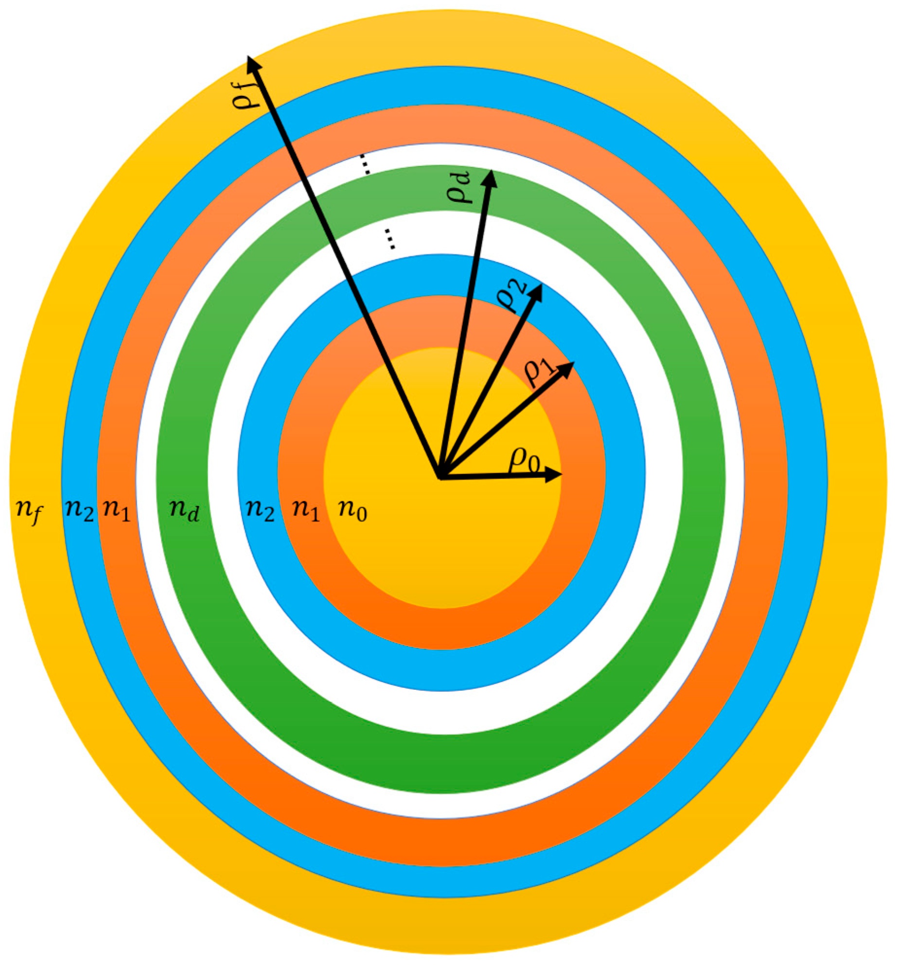
Figure 2.
Reflectance spectrum of Si/SiO2 annular photonic crystal with PS and PMMA as the defect layers.
Figure 2.
Reflectance spectrum of Si/SiO2 annular photonic crystal with PS and PMMA as the defect layers.
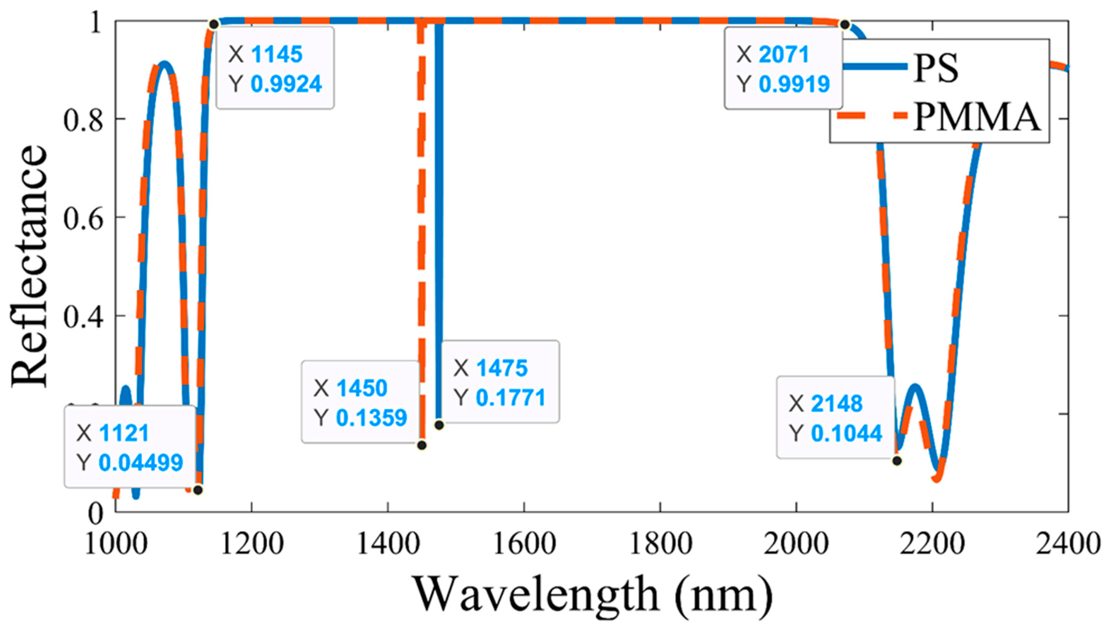
Figure 3.
Reflectance of the annular photonic crystal with PS as a defect layer at different pressures.
Figure 3.
Reflectance of the annular photonic crystal with PS as a defect layer at different pressures.
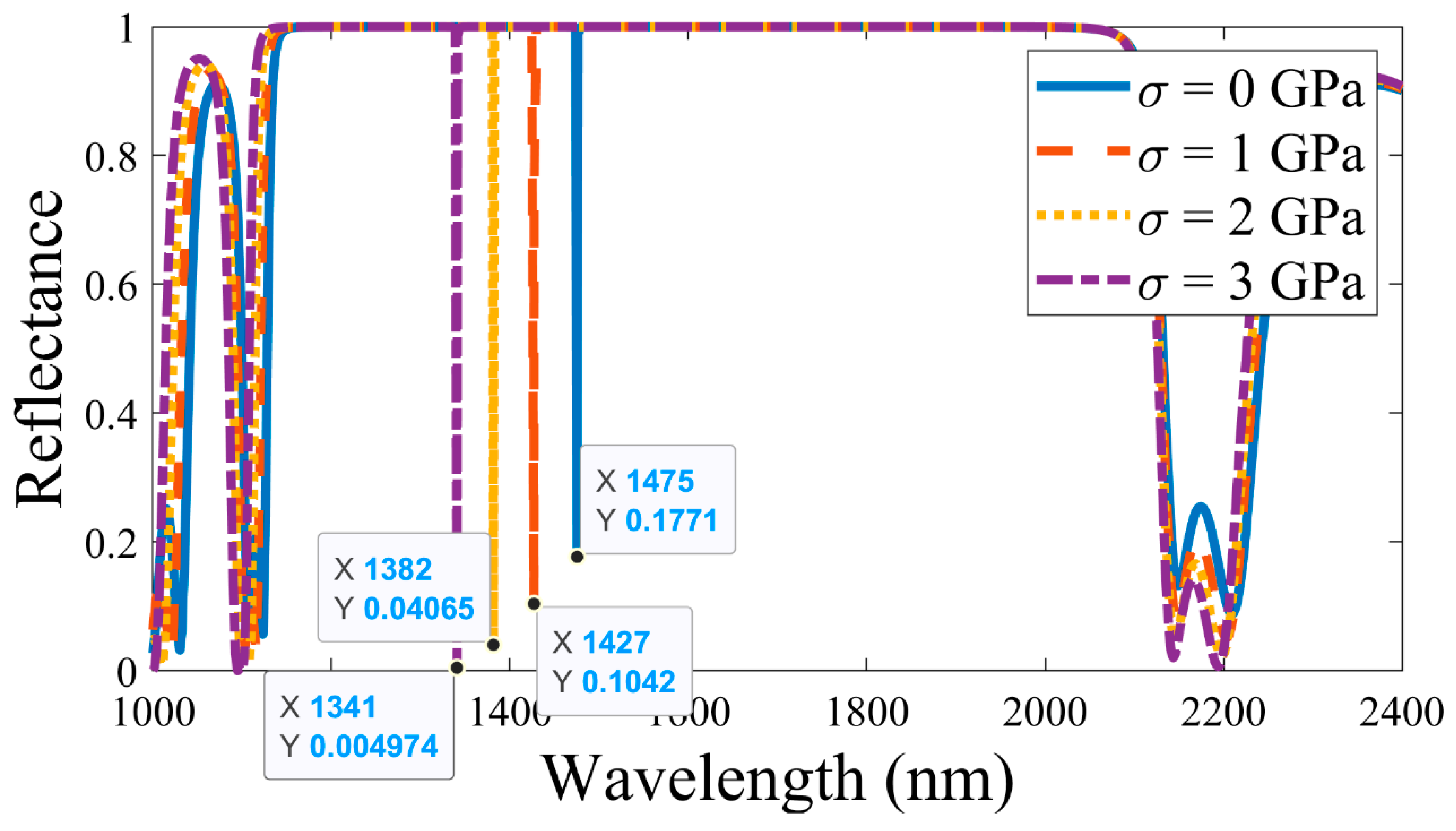
Figure 4.
Reflectance of the annular photonic crystal with PMMA as a defect layer at different pressures.
Figure 4.
Reflectance of the annular photonic crystal with PMMA as a defect layer at different pressures.
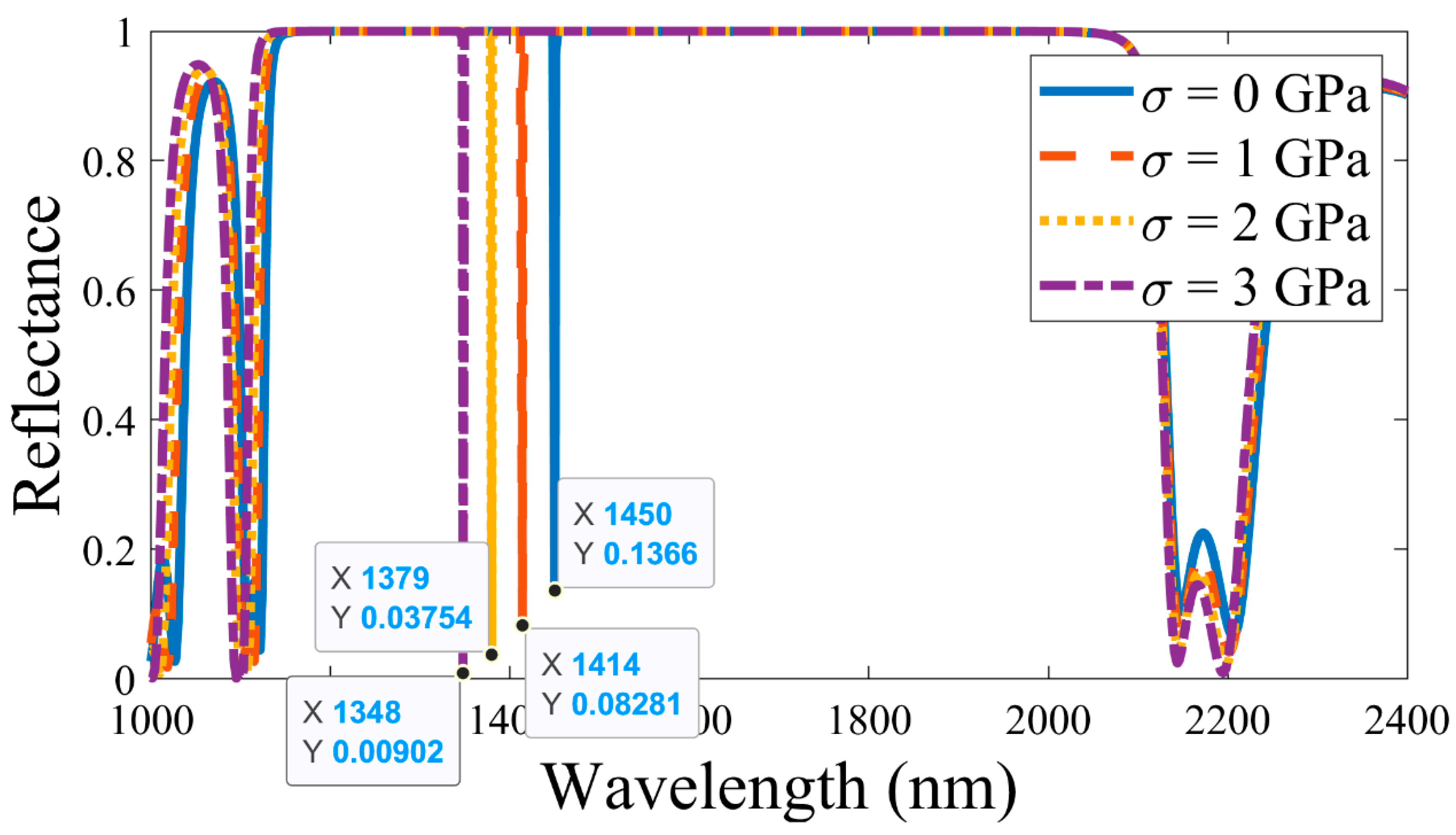
Figure 5.
Variation in the defect peak positions with pressure variation.
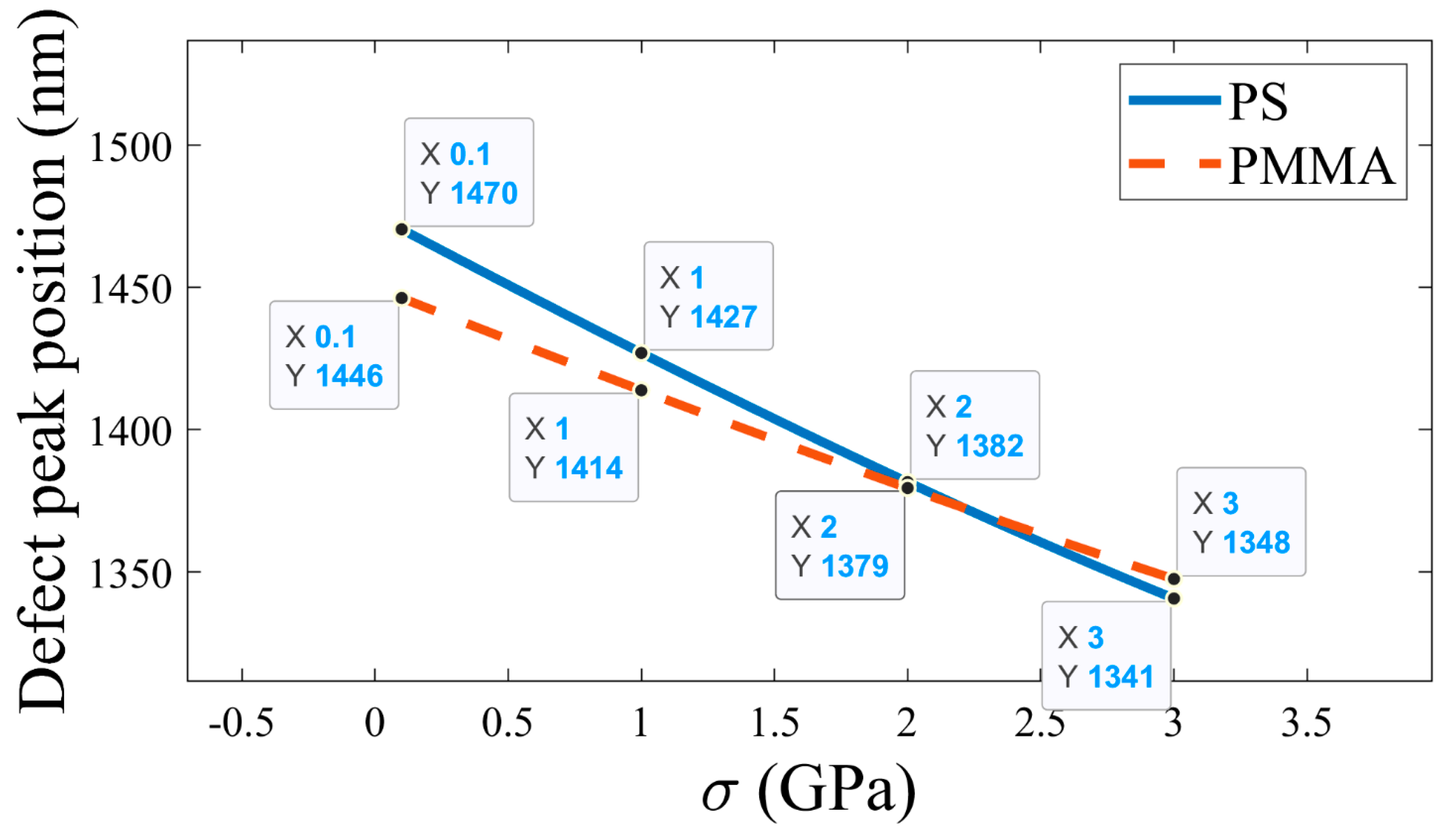
Figure 6.
Variation in the intensity of the defect peak with pressure variation.
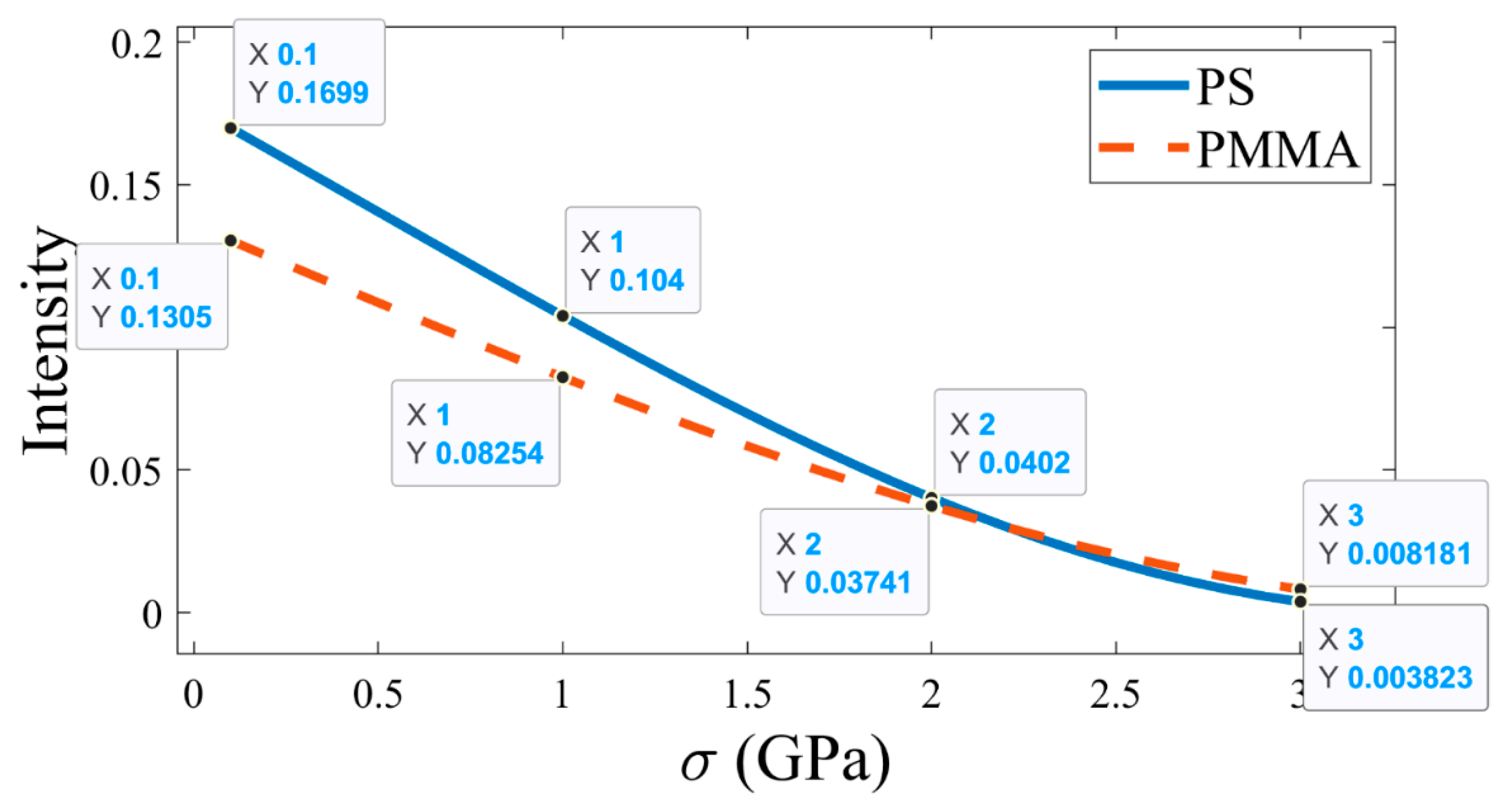
Figure 7.
Analysis of pressure sensitivity of two annular photonic crystals with defects PS and PMMA.
Figure 7.
Analysis of pressure sensitivity of two annular photonic crystals with defects PS and PMMA.
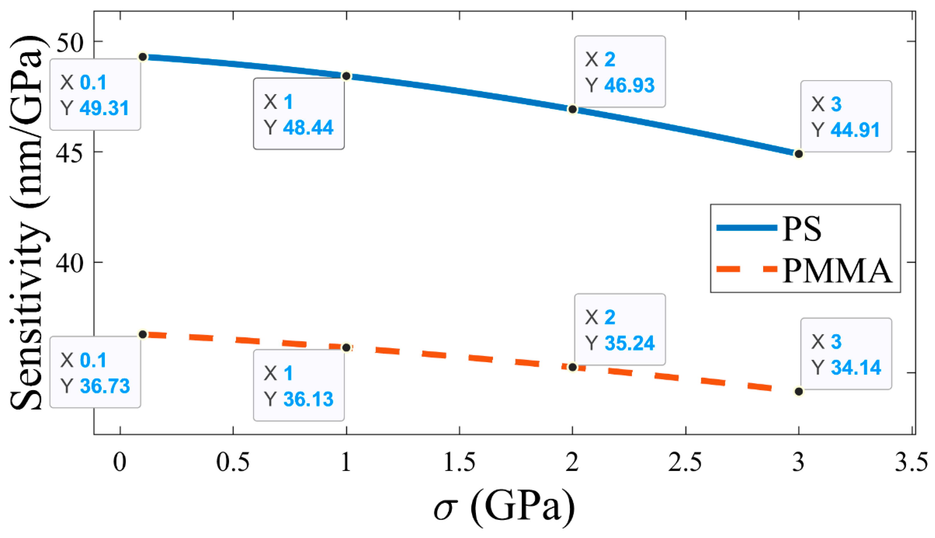
Figure 8.
Reflectance of the APC with PS as a defect layer with pressure variation.
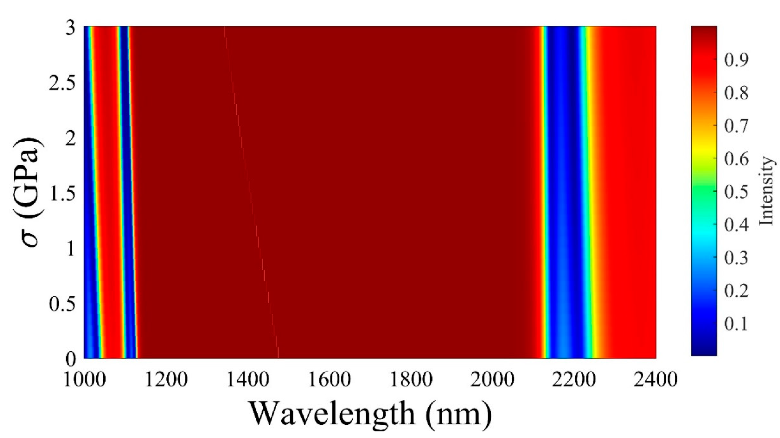
Figure 9.
Reflectance with PMMA as a defect layer for APC with pressure variation.
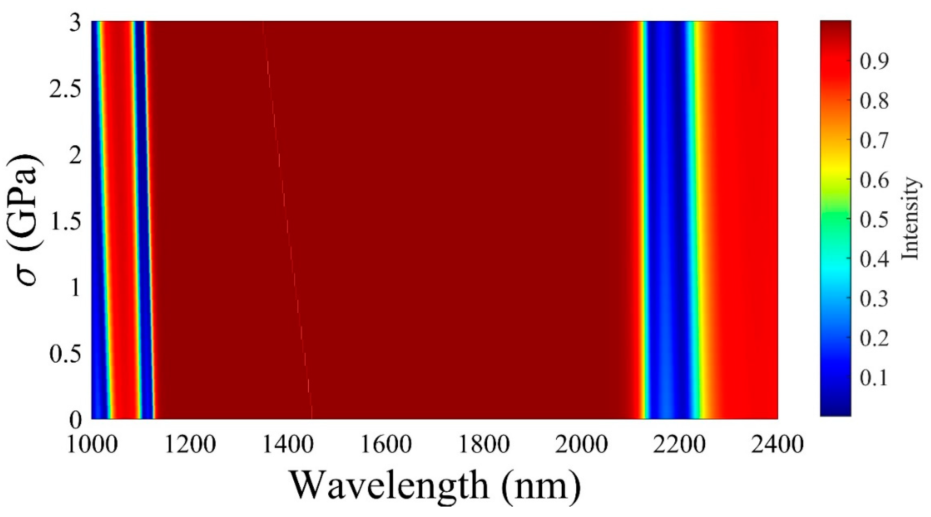
Figure 10.
Variation in sensitivity with changes in the defect layer thickness; sensitivity is measured between 0 GPa and 3 GPa.
Figure 10.
Variation in sensitivity with changes in the defect layer thickness; sensitivity is measured between 0 GPa and 3 GPa.
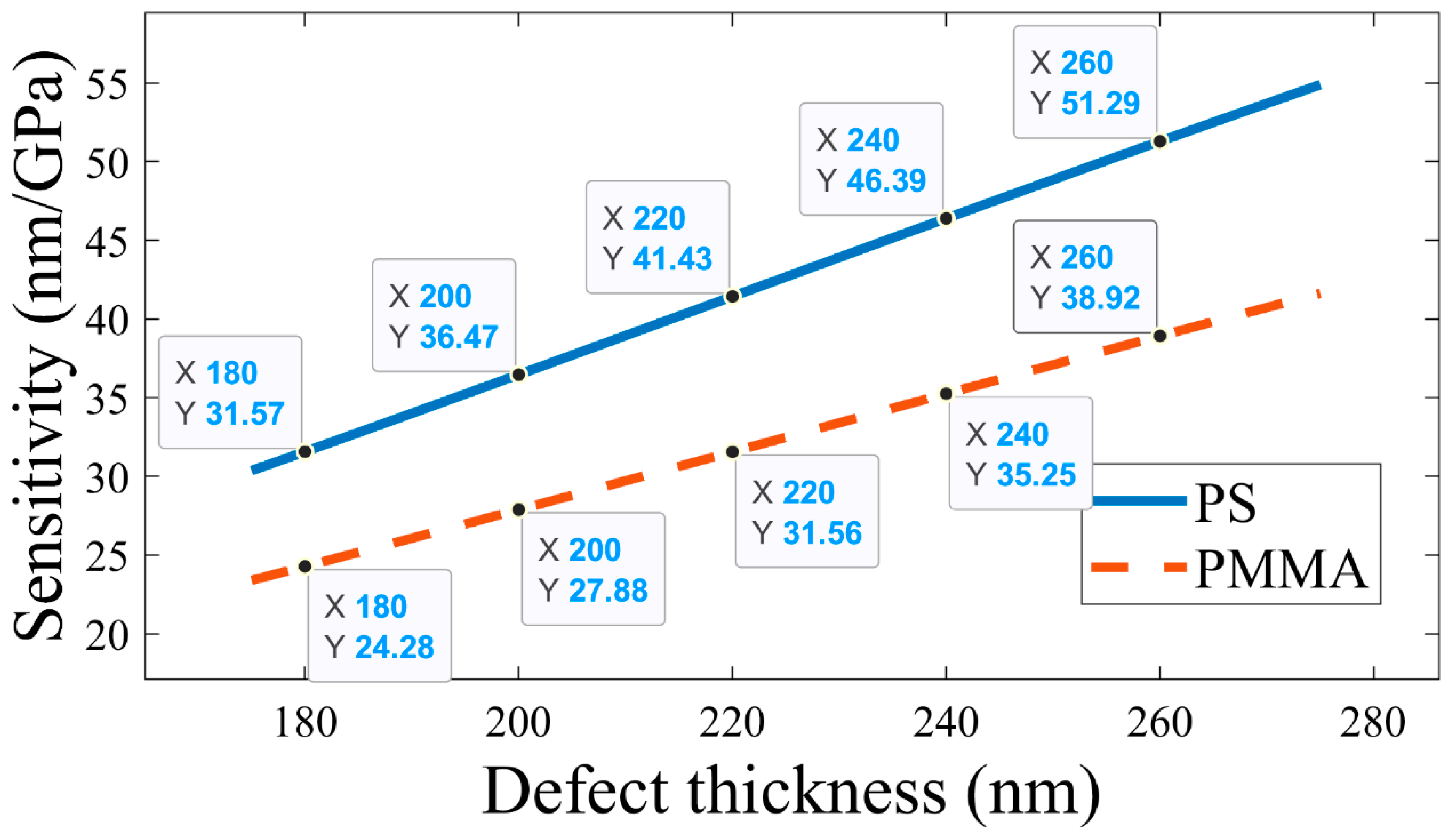
Figure 11.
Change in the Figure of Merit with changes in the defect layer thickness.
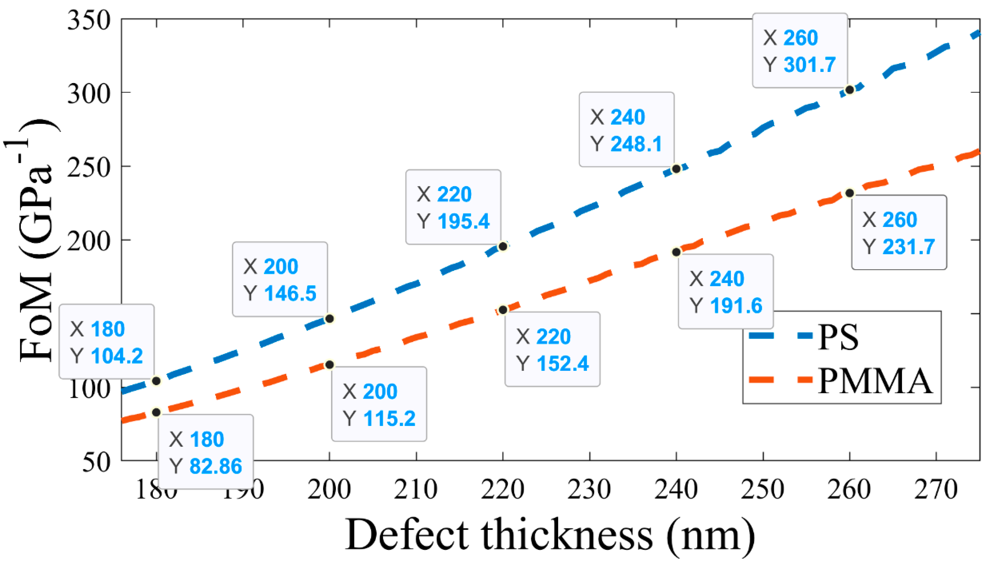
Figure 12.
Variation in sensitivity with changes in the periodicity number; sensitivity is measured between 0 GPa and 3 Gpa.
Figure 12.
Variation in sensitivity with changes in the periodicity number; sensitivity is measured between 0 GPa and 3 Gpa.
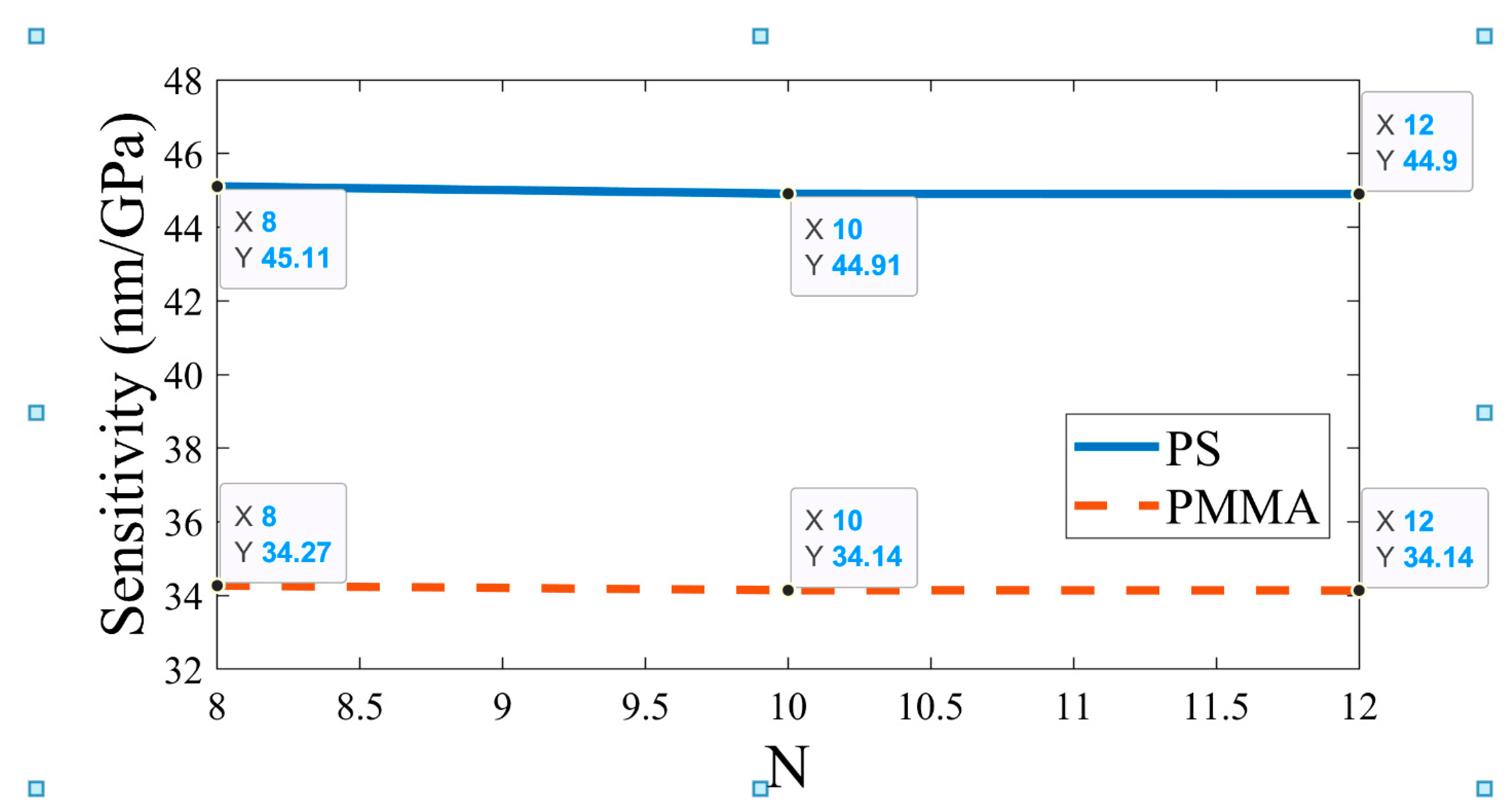
Figure 13.
Variation in the Figure of Merit with changes in the periodicity number.
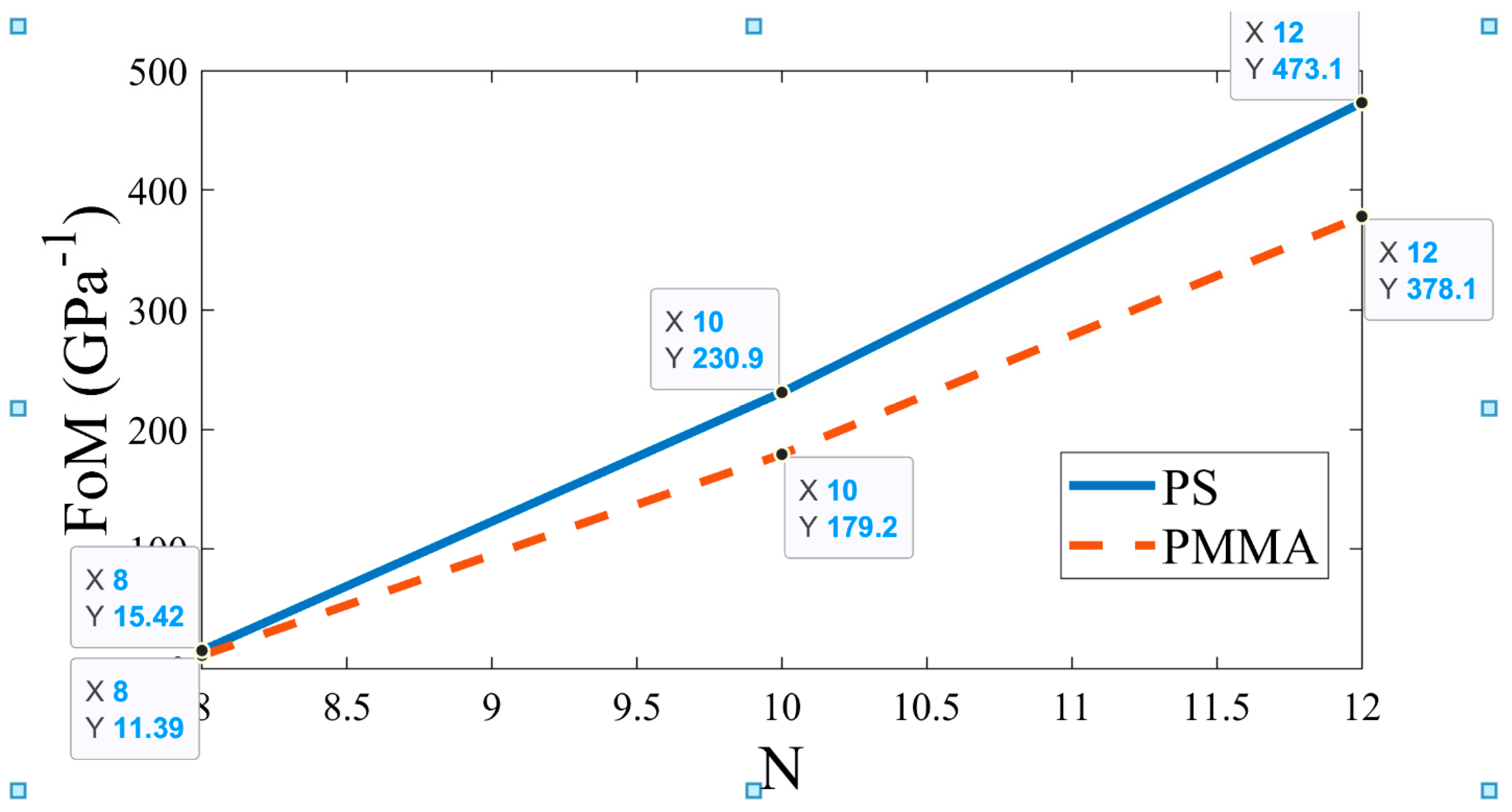

Table 1.
Evaluation of the sensor’s performance parameters for the PS defect-based APC.
| Defect peak intensity |
Sensitivity |
Quality factor |
Figure of merit |
|||
|---|---|---|---|---|---|---|
| 0 | 1475.4 | 0.177 | N/A | 0.234 | 6305.1 | N/A |
| 1 | 1427.0 | 0.104 | 48.4 | 0.204 | 6994.9 | 237.5 |
| 2 | 1381.5 | 0.040 | 46.9 | 0.192 | 7195.5 | 244.4 |
| 3 | 1340.7 | 0.004 | 44.9 | 0.193 | 6946.5 | 232.7 |
Table 2.
Evaluation of the sensor’s performance parameters for the PMMA defect-based APC.
| Defect peak intensity |
Sensitivity |
Quality factor |
Figure of merit |
|||
|---|---|---|---|---|---|---|
| 0 | 1449.9 | 0.135 | N/A | 0.224 | 6473.0 | N/A |
| 1 | 1413.8 | 0.083 | 36.1 | 0.203 | 6964.6 | 178.0 |
| 2 | 1379.5 | 0.037 | 35.2 | 0.192 | 7184.7 | 183.6 |
| 3 | 1347.5 | 0.008 | 34.1 | 0.190 | 7092.2 | 179.7 |
Disclaimer/Publisher’s Note: The statements, opinions and data contained in all publications are solely those of the individual author(s) and contributor(s) and not of MDPI and/or the editor(s). MDPI and/or the editor(s) disclaim responsibility for any injury to people or property resulting from any ideas, methods, instructions or products referred to in the content. |
© 2023 by the authors. Licensee MDPI, Basel, Switzerland. This article is an open access article distributed under the terms and conditions of the Creative Commons Attribution (CC BY) license (http://creativecommons.org/licenses/by/4.0/).
Copyright: This open access article is published under a Creative Commons CC BY 4.0 license, which permit the free download, distribution, and reuse, provided that the author and preprint are cited in any reuse.


