Submitted:
06 May 2023
Posted:
09 May 2023
You are already at the latest version
Abstract
Recently, resistive random access memory (RRAM) has been an outstanding candidate among various emerging nonvolatile memories for high density storage and in-memory computing applications. However, the traditional RRAM, which accommodates two states depending on applied voltage, cannot meet the high density requirement in the era of big data. Many research groups have demonstrated that RRAM possesses the possibility of multi-level cell to overcome the demand of mass storage. Among numerous semiconductor materials, gallium oxide, as the fourth-generation semiconductor material, is highly-profile due to its excellent material proper-ties, and already be widely used in optoelectronics, high-power, resistive switching device and so on, due to its wide bandgap and transparent properties. In this study, we have successfully demonstrated the Al/GO/Ga2O3/ITO RRAM to achieve the possibility of two-bit storage. Compared to the single-layer counterpart, the bilayer structure has excellent electrical properties and stable reliability. The endurance characteristics could be enhanced above 100 switching cycles with an ON/OFF ratio of over 103. Moreover, the filament models are also described in this thesis to clarify the transport mechanisms.
Keywords:
RRAM
; Gallium oxide
; Graphene oxide
; Bilayer structure
; Multilevel storage
1. Introduction
IN 20 century, D. Kahng and S. M. Sze proposed a floating gate (FG) device to obtain the non-volatility characteristic in memory applications. This was the first time that the possibility of nonvolatile MOS memory was recognized. It is worth mentioning that flash memory, based on the MOSFET transistors with a floating gate, has become a common component of USB flash drive and solid-state disk (SSD) [1].
Due to the physical limit, DRAM, SRAM, and flash memory are currently facing challenges to scale down to 10 nm node. It has become much difficult and expensive to enhance the performance and reliability. At first, the Silicon-Oxide-Nitride-Oxide-Silicon (SONOS) flash memory, which uses a silicon nitride as a charge trapping layer, relieves the problems caused by scaling down. However, when the gate oxide thickness is down to about 7 nm, the scaling-down problems are also inevitable [2].
RRAM, comprised of a simple capacitor-like structure, has great potential to replace the flash memory and DRAM, becoming the next-generation non-volatile memory. A great number of kinds of materials have been research for acting as resistive switching layers, such as binary metal oxides, perovskite oxides, and chalcogenide materials. Above them, the binary metal oxides, like HfOx, TiOx, AlOx, ZrOx, have been the great candidates for the use of switching layer owing to the simplicity of materials and good compatibility with silicon CMOS fabrication. Thus, many research activities have bloomed with a few demonstrations of various RRAM structure with insulator layer of various binary metal oxides [3,4]. Wide bandgap materials, especially HfO2 (around 5.7 eV), play important roles in many fields of semiconductor industry, such as MOSFET, RRAM, laser diode. Ga2O3, which is thought of as the fourth-generation semiconductor material, has been demonstrated that it is one of promising material to replace GaN and SiC because of wide bandgap of 4.9 eV in -phase and high breakdown field. Therefore, it is considered as the most appropriate candidate of high-power devices. However, few group have researched Ga2O3 material for memory applications. Based on the quantum effect, the amorphous-phase Ga2O3 (a-Ga2O3) is more suitable than -phase Ga2O3 (-Ga2O3) as the switching layer of RRAM because the leakage current is smaller and the bandgap of a-Ga2O3 is also quite large [5].
In this study, the bilayer Al/GO/a-Ga2O3/ITO RRAM was proposed and the monolayer Al/a-Ga2O3/ITO RRAM was also fabricated to draw a comparison between two structures. Compared with the monolayer structure, the bilayer one had better electrical properties and reliability characteristics. The multilevel characteristic was presented through modulating the current compliance, and the possibility of lower power consumption was also demonstrated due to lower operation voltage and current compliance.
2. Results and Discussion
Figure 1 shows the element distribution analyzed through energy dispersive spectroscopy (EDS) mapping. Based on this mapping, the relative positions of all elements can be clearly distinguished. The EDS mapping can also prove the scavenging phenomenon between the Al top electrode and the GO layer. The crystal structure analysis of Ga2O3 thin film on a glass substrate is depicted in Figure 2 (a). This result shows that the structure of Ga2O3 deposited by RF sputtering was in amorphous phase. For the purpose of the low leakage current in RRAM devices, the amorphous phase is better than crystalline phase [6]. It is noteworthy that the peak around 24 degrees was attributed to the substrate [7]. The bandgap of Ga2O3 varies in different phase [8,9]. In this measurement, the bandgap of the Ga2O3 film was confirmed by a U-3310 spectrophotometer, as shown in Figure 2 (b). The bandgap of Ga2O3 in amorphous phase is around 4.25eV.
The electrical properties of monolayer and bilayer structures were characterized by an Agilent B1500A parameter analyzer. The ITO bottom electrode was grounded, and the applied voltage was exerted on the Al top electrode. Figure 3 shows the resistive switching behaviors of the Al/Ga2O3/ITO/glass RRAM device and Al/GO/Ga2O3/ITO/glass RRAM device. The forming processes of Al/Ga2O3/ITO/glass and Al/GO/Ga2O3/ITO/glass RRAMs devices occurred under negative voltage sweeps (0V→-10V→0V) at -50 mV intervals, and the compliance current was set to 10 mA to prevent the device from soft breakdown of the devices. In Figure 3 (a), the forming voltage of the Al/Ga2O3/ITO/glass RRAM device and Al/GO/Ga2O3/ITO/glass RRAM device were -7.3 V, -5.65 V, respectively. Figure 3 (b) show the I-V curve of the SET and RESET process of the device. Obviously, the I-V curves exhibited bipolar switching behavior in both structures. The SET/RESET processes occurred under applied negative voltage sweeps (0 V→-4 V→ 0 V) and positive voltage sweeps (0 V→+4 V→0 V), respectively, and the compliance current was set to 100 mA. For monolayer structure RRAM, the set voltage and reset voltage were -1.2 V and 2.95 V, respectively. The ON/OFF ratio was approximately 104 at -0.1 volts. The Vset and Vreset of Al/GO/Ga2O3/ITO/glass is -0.9 V and 2.65 V, respectively. The ON/OFF ratio was approximately 103 at -0.1 volts.
So as to investigate the conduction mechanism of Al/Ga2O3/ITO/glass and Al/GO/Ga2O3/ITO/glass RRAMs in the LRS and HRS, the DC I-V characteristics were fitted after we programed the device. Figure 6 shows the fitting results of the I-V characteristics. According to the Ohmic conduction equation (V=IR), the current conduction is dominated by Ohmic conduction if the slope of ln(I)-ln(V) is close to 1. For Al/Ga2O3/ITO/glass and Al/GO/Ga2O3/ITO/glass structures, the slope of LRS in the low-voltage region is around 1.00, which indicates that the current conduction behavior is Ohmic conduction, as shown in Figure 4 (a)-(b). Moreover, if the I-V curve plotted using ln-ln scale in HRS exhibits a complicated shape, the conduction mechanism is dominated by Space-Charge-Limited Conduction (SCLC). In the low-voltage region, the slope of HRS is approximately 1. As the bias voltage increases, the slope increases to 2 in the square region. When the bias voltage further increases, the current in HRS increases rapidly and the slope is much sharp in high-voltage region [10]. For Al/Ga2O3/ITO/glass device, the slope in the HRS region changed from 1.19 to 2.02 to 3.21 with increasing voltage, which can be explained by the SCLC, as shown in Figure 4 (c). For Al/GO/Ga2O3/ITO/glass device, the slope of 1.05, 2.06, and 3.14 were obtained in low-voltage, square, and high-voltage regions (Figure 4 (d)), indicating that the conduction mechanism follows SCLC. Furthermore, the fitting results of HRS using Schottky emission (ln(I)∝V1/2) and Poole-Frenkel (ln(I/V) ∝V1/2), as shown in Figure 4 (c)-(d). The results were not fitted well by these two mechanisms.
Figure 5 (a) show the endurance tests of DC resistive switching. The current values were extracted at -0.1 V in the test. The Al/Ga2O3/ITO structure can maintain the ON/OFF ratio around 104 only after 28 DC switching cycles. This result demonstrates that the Al/Ga2O3/ITO structure was not stable for resistive switching. However, The Al/GO/Ga2O3/ITO structure can maintain the ON/OFF ratio around 103 after 126 DC switching cycles. This result demonstrates that the GO insertion layer played a key role in improvement of endurance test. Figure 5 (b) show the retention performance of HRS and LRS without any considerable degradation in the resistance was observed after 104 s at room temperature, indicating the device’s stability and non-volatile storage properties.
Based on the filament theory, the non-uniformity is an essential issue for RRAM device due to the random conformation and rupture during set and reset processes, respectively. Two parameters generally observed in resistive switching characteristics to quantify the non-uniformity are cycle-to-cycle uniformity and device-to-device uniformity.
Figure 6 (a) shows the current distribution of HRS and LRS. The current values in both states were measured at read voltage of -0.1 volts and the compliance current of 100 mA. Figure 6 (a) shows the result of cycle-to-cycle variation of Al/Ga2O3/ITO device in LRS at the average value was 3.61×10⁻³, and the coefficient of variation was about 20%. In HRS at the average value was 7.21×10⁻⁷, and the coefficient of variation was about 83%. The HRS was not uniform during resistive switching. The result of cycle-to-cycle variation of Al/GO/Ga2O3/ITO device in LRS at the average value was 3.04×10⁻³, and the coefficient of variation was about 11%. In HRS at the average value was 3.31×10⁻⁶, and the coefficient of variation was about 49%. Figure 6 (b) shows that the VSET has about 19% probability to be at −1.66 V, and VRESET has about 39% probability to be at 2.97 V for Ga2O3 devices. The mean and standard deviation of VSET/VRESET for GO/Ga2O3 devices are −1.04 V/17% and 2.59 V/30%, respectively. The distribution of switching voltages VSET and VRESET is very concentrated highlighting the good uniformity.
Multi-level cell (MLC) storage is the simplest technology to accommodate more information with low cost for high density storage applications. RRAM has particularly attracted lots of attention owing to its simplicity of obtaining the multi-state characteristics. In the bilayer structure, the switching layer can be distinguished into vacancy-rich region and vacancy-deficient region owing to the intrinsic nature of defect generation. The filament can be well controlled in the vacancy-poor region by modulating the current compliance, which further obtains the multiple LRS to achieve MLC storage capability [11,12]. Figure 7 (a) show the I-V characteristics of Al/GO/Ga2O3/ITO device at compliance currents of 100 mA, 10 mA and 1 mA, respectively.
Figure 7 (b) show the endurance characteristics of Al/GO/Ga2O3/ITO device at 100 mA, 10 mA and 1 mA current compliance. The ON/OFF ratio can maintain over 103 after 126 DC cycles at 100 mA compliance current. The ON/OFF ratio can maintain over 103 after 161 DC cycles at 10 mA compliance current and after 178 DC cycles at 1mA compliance current. Figure 7 (c) shows the retention characteristics of bilayer device at 100 mA, 10mA and 1mA current compliance, respectively. The result exhibits the possibility of 2-bit storage, including three LRS and 1HRS [13]. Figure 7 (d) shows the current distribution of HRS and LRS to assess the device-to-device uniformity. Five different devices on the sample were randomly selected to conduct the DC I-V measurement for 5 cycles. The voltage sweeping from -4V to 4V was applied on all devices. For this analysis, the current values were also extracted at -0.1 volts. The results of device-to-device variation for GO/Ga2O3 at 100 mA, 10 mA and 1 mA are also presented. Because of the GO layer, the GO/Ga2O3 device had excellent device-to-device uniformity.
The results of cycle-to-cycle variation of Al/GO/Ga2O3/ITO device at the compliance current of 100 mA, 10mA and 1mA are also shown in Figure 8. The GO/Ga2O3 device values of coefficient of variation in LRS and HRS were about 11% and 49% at 100 mA. The GO/Ga2O3 device values of coefficient of variation in LRS and HRS were about 12% and 50% at 10 mA. The GO/Ga2O3 device values of coefficient of variation in LRS and HRS were about 7% and 39% at 1 mA. Compared to the single-layer structure, the bilayer structure had better cycle-to-cycle uniformity because of the presence of GO insertion layer.
Figure 9 (a) plots the dependences between pattern sizes and resistive states of Al/GO/Ga2O3/ITO/glass device at 10 mA current compliance. The resistance values were extracted at -0.1V. This result demonstrates that both states were insensitive to the pattern sizes. Thus, the filament theory is appropriate to explain the operation of resistive switching for this structure. Figure 9 (b) shows the relationship between both states and temperatures at 10mA current compliance. This result was characterized by an Agilent B1500A parameter analyzer, and the sample was heated ranging from 300K to 500K. In this measurement, the resistance values were also extracted at -0.1 volts under different temperatures. The resistance of HRS decreased with increasing temperature, which exhibited a semiconductor-like behavior. On the other hand, the current of LRS maintained at a fixed value under different temperatures. It is worth noting that the memory window still maintained around 102 under the high temperature of 500K, which could be attributed to the wide bandgap of Ga2O3.
Filament theory is the most widely used theory to elucidate the resistive switching mechanism of RRAM devices. It means the switching behavior relies on the conformation and rupture of the conductive filament (CF) in the switching layer [14,15]. In order to explain the resistive switching mechanism, filament models of the Al/Ga2O3/ITO/glass and the Al/GO/Ga2O3/ITO/glass are constructed in Figure 10, respectively. The distributions of oxygen vacancies before conducting electrical measurements are presented in Figure 10 (a)-(b). In Figure 10 (a), the presence of the oxygen vacancies in ITO makes the forming and set processes under the negative sweep, and reset process under the positive sweep. In Figure 10 (b), the high concentration of oxygen vacancies makes the forming voltage lower. The distributions of oxygen vacancies under resistive switching (set and reset processes) of both devices are shown in Figure 10 (c)-(f). Owing to the GO insertion layer, the conformation and rupture of CFs could be more uniform and CFs could be thinner than the pristine device. Moreover, the CFs could be modulated by different compliant currents.
3. Conclusions
In this study, the Al/GO/Ga2O3/ITO/glass RRAM structure was demonstrated. Compared with Ga2O3 monolayer structure, bilayer RRAM had better electrical properties, for instance, lower forming and set/reset voltages, and better endurance. Based on the filament theory, the formation of conductive filament, which is composed of oxygen vacancies, can affect the resistive switching. Because of the GO layer, the switching layer can be distinguished into vacancy-rich region (GO) and vacancy-deficient region (Ga2O3), which helped us to control the conformation and rupture of CF in order to optimize the endurance characteristics. The endurance was improved to more than 100 cycles, which was 5 times higher. Moreover, the IV characteristics and endurance test, modulated by decreasing the compliance current to 100 mA, 10 mA and 1 mA to achieve the multi-level cell (MLC) technology, were also demonstrated. It is an excellent technology to accommodate much data with low cost. Furthermore, the bilayer RRAM had stable retention more than 104 seconds without significant degradation in all states. Finally, the filament models are also described to explain the conformation and rupture in the resistive switching layers of both structures.
4. Materials and Methods
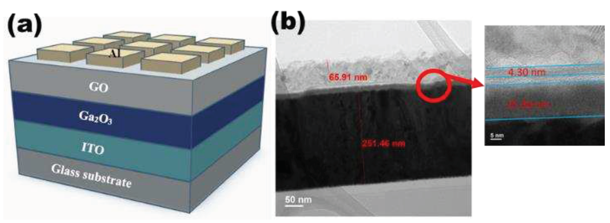
The schematic of Al/GO/Ga2O3/ITO structure is shown in Figure 11 (a). The RRAM device was fabricated on a commercial ITO/glass substrate. We used the ITO layer as bottom electrode (BE). The RF sputtering was operated at a power of 90 W and a working pressure of 6mTorr under Ar/O2 flow of 25/25sccm for 10 minutes to deposit a 15nm Ga2O3 switching layer. Graphite and potassium permanganate were slowly added to a mixture of sulfuric and phosphoric acids at room temperature and stirred for 24 hours. The mixture was then treated with water and hydrochloric acid until the pH was neutral. Finally, graphene was obtained in two centrifugation steps at 6000 rpm for 3 hours. Graphene oxide solution was obtained by dissolving graphene in water. Then, the graphene oxide solution was spin-coated on Ga2O3/ITO/glass samples at 700/1000 rpm for 20/40 sec and vacuum baked at 60°C for 10 min to obtain graphene oxide films [16,17]. Finally, the 66nm Al top electrode (TE) patterned by a shadow mask with 0.25 mm2 holes was deposited using DC sputtering on the GO/Ga2O3/ITO/glass sample. Furthermore, the Al/Ga2O3/ITO/glass structure was also fabricated for comparison. The electrical measurements were carried out by Agilent B1500A semiconductor parameter analyzer. The bias was applied on the TE and the BE was grounded. Figure 11 (b) depicts the TEM image of device cross-section. It is worth noting that a sub-AlOx interfacial layer was form between the Al metal layer and GO layer, because the Al scavenged the oxygen ions from the GO layer. Besides, the thickness values of GO layer and AlOx layer are ~4 nm and ~4nm, respectively.
Author Contributions
Conceptualization, validation, formal analysis, investigation, and data curation L.-W.W., C.-W.H. and K.-J.L; writing—original draft, C.-W.H. and K.-J.L.; writing—review and editing, K.-J.L.; supervision, S.-Y.C. and Y.-H.W. All authors have read and agreed to the published version of the manuscript.
Funding
This work was supported in part by the Ministry of Science and Technology of Taiwan under Grant MOST 108-2221-E-006-040-MY3 and MOST 111-2221-E-006-206.
Institutional Review Board Statement
Not applicable.
Informed Consent Statement
Not applicable.
Data Availability Statement
Not applicable.
Acknowledgments
Not applicable.
Conflicts of Interest
The authors declare no conflict of interest.
References
- Kahng, D.; Sze, S.M. A Floating Gate and Its Application to Memory Devices. Bell Syst. Tech. J. 1967, 46, 1288–1295. [Google Scholar] [CrossRef]
- Meena, J.S.; Sze, S.M.; Chand, U.; Tseng, T.-Y. Overview of emerging nonvolatile memory technologies. Nanoscale Res. Lett. 2014, 9, 526–526. [Google Scholar] [CrossRef] [PubMed]
- Zahoor, F.; Zulkifli, T. Z. A.; Khanday, F. A. ; Resistive Random Access Memory (RRAM): an Overview of Materials, Switching Mechanism, Performance, Multilevel Cell (mlc) Storage, Modeling, and Applications. Nanoscale Research Letters. 2020, vol. 15, no. 1, pp. 90-90. [CrossRef]
- Pal, P.; Lee, K. J.; Chang, T.C.; Singh, A.; Thunder, S.; De, S.; Huang, P. T.; Kämpfe, T.; Wang, Y. H. ; Flexible Precision Bending Resistant Multi-bit Memristor for Inference Engine Application. IEEE Tr. ED..2022, Vol. 69, no. 8, pp 4737-4743.
- Lim, H.; Kim, D.; Cha, S.Y.; Mun, B.S.; Noh, D.Y.; Kang, H.C. Crystallization and bandgap variation of non-stoichiometric amorphous Ga2O3-x thin films during post-annealing process. Appl. Surf. Sci. 2022, 585, 152771. [Google Scholar] [CrossRef]
- Wang, W.; Dong, G.; Wang, L.; Qiu, Y. ; Pentacene thin-film transistors with sol–gel derived amorphous Ba0.6Sr0.4TiO3 gate dielectric. Microelectronic Engineering. 2008, vol. 85, no. 2, pp. 414-418. [CrossRef]
- Mikhalitsyna, E. A. ; Kataev,V. A.; Larrañaga, A.; Lepalovskij, V. N.; Kurlyandskaya, G. V; Nanocrystallization in FINEMET-Type Fe73.5Nb3Cu1Si13.5B9 and Fe72.5Nb1.5Mo2Cu1.1Si14.2B8.7 Thin Films. Materials. 2020, vol. 13, no. 2, pp. 348. [CrossRef]
- Lee, S. H.; Kim, S. B.; Moon, Y. J.; Kim, S. M.; Jung, H. J.; Seo, M. S.; Lee, K. M.; Kim, S. K.; Lee, S. W. ; High-Responsivity Deep-Ultraviolet-Selective Photodetectors Using Ultrathin Gallium Oxide Film. ACS Photonics. 2017, vol. 4, no. 11, pp. 2937-2943, 2017.
- Kim, J.; Sekiya, T.; Miyokawa, N.; Watanabe, N.; Kimoto, K.; Ide, K.; Toda, Y.; Ueda, S.; Ohashi, N.; Hiramatsu, H.; et al. Conversion of an ultra-wide bandgap amorphous oxide insulator to a semiconductor. NPG Asia Mater. 2017, 9, e359–e359. [Google Scholar] [CrossRef]
- Liu, K. C.; Tzeng, W. H.; Chang, K. M.; Chan, Y. C.; Kuo, C. C.; Cheng, C. W. ; The resistive switching characteristics of a Ti/Gd2O3/Pt RRAM device. Microelectronics and Reliability. 2010, vol. 50, no. 5, pp. 670-673. [CrossRef]
- Swathi, S.; Angappane, S. Low power multilevel resistive switching in titanium oxide-based RRAM devices by interface engineering. J. Sci. Adv. Mater. Devices 2021, 6, 601–610. [Google Scholar] [CrossRef]
- Prakash, A.; Song, J.; Lim, S.-J.; Park, J.-H.; Woo, J.; Cha, E.; Hwang, H. Multi-state resistance switching and variability analysis of HfOx based RRAM for ultra-high density memory applications. 2015 International Symposium on Next-Generation Electronics (ISNE). LOCATION OF CONFERENCE, TaiwanDATE OF CONFERENCE; pp. 1–2.
- Pal, P.; Wang, Y.H. Interconversion of complementary resistive switching from graphene oxide based bipolar multilevel resistive switching device. Appl. Phys. Lett. 2020, 117, 054101. [Google Scholar] [CrossRef]
- Qi, M.; Cao, S.; Yang, L.; You, Q.; Shi, L.; Wu, Z. Uniform multilevel switching of graphene oxide-based RRAM achieved by embedding with gold nanoparticles for image pattern recognition. Appl. Phys. Lett. 2020, 116, 163503. [Google Scholar] [CrossRef]
- Sawa, A. Resistive switching in transition metal oxides. Mater. Today 2008, 11, 28–36. [Google Scholar] [CrossRef]
- Lee, K.-J.; Weng, Y.-C.; Wang, L.-W.; Lin, H.-N.; Pal, P.; Chu, S.-Y.; Lu, D.; Wang, Y.-H. High Linearity Synaptic Devices Using Ar Plasma Treatment on HfO2 Thin Film with Non-Identical Pulse Waveforms. Nanomaterials 2022, 12, 3252. [Google Scholar] [CrossRef] [PubMed]
- Lee, K.-J.; Wang, Y.-H. ; Effect of Alkaline Earth Metal on AZrOx (A = Mg, Sr, Ba) Memory Application. Gels. 2022, vol.8, p. 20.
Figure 1.
EDS mapping of the cross-section profile of the device.
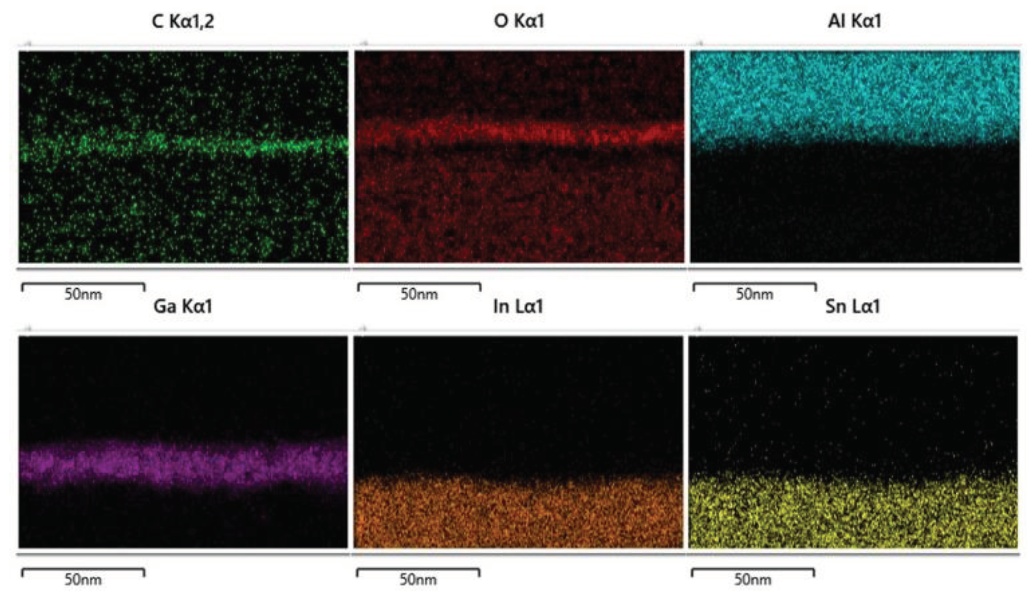
Figure 2.
(a) The XRD result of Ga2O3 thin film on a glass substrate. (b) The result of bandgap of Ga2O3 measured by spectrophotometer.
Figure 2.
(a) The XRD result of Ga2O3 thin film on a glass substrate. (b) The result of bandgap of Ga2O3 measured by spectrophotometer.
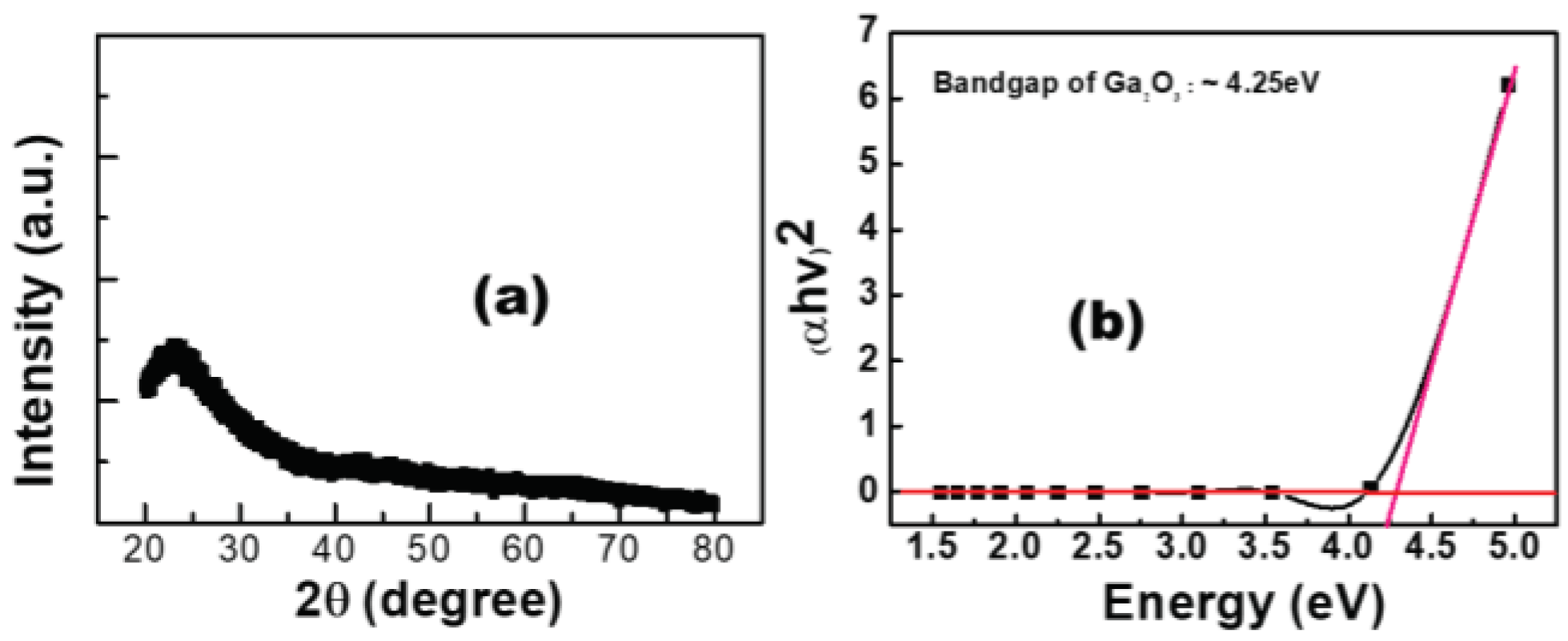
Figure 3.
(a) Forming curves of Al/Ga2O3/ITO/glass and Al/GO/Ga2O3/ITO/glass devices RRAMs. (b) I-V switching curves of the Al/Ga2O3/ITO/glass and Al/GO/Ga2O3/ITO/glass devices RRAMs.
Figure 3.
(a) Forming curves of Al/Ga2O3/ITO/glass and Al/GO/Ga2O3/ITO/glass devices RRAMs. (b) I-V switching curves of the Al/Ga2O3/ITO/glass and Al/GO/Ga2O3/ITO/glass devices RRAMs.
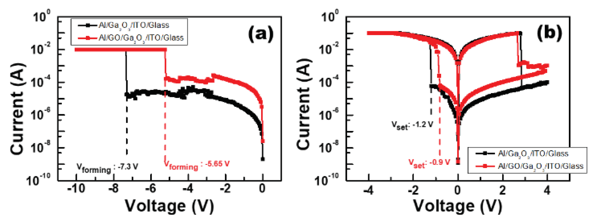
Figure 4.
Fitting results for the (a) Ga2O3 and (b) GO/Ga2O3 devices in LRS and (c) Ga2O3 and (d) GO/Ga2O3 devices at HRS.
Figure 4.
Fitting results for the (a) Ga2O3 and (b) GO/Ga2O3 devices in LRS and (c) Ga2O3 and (d) GO/Ga2O3 devices at HRS.
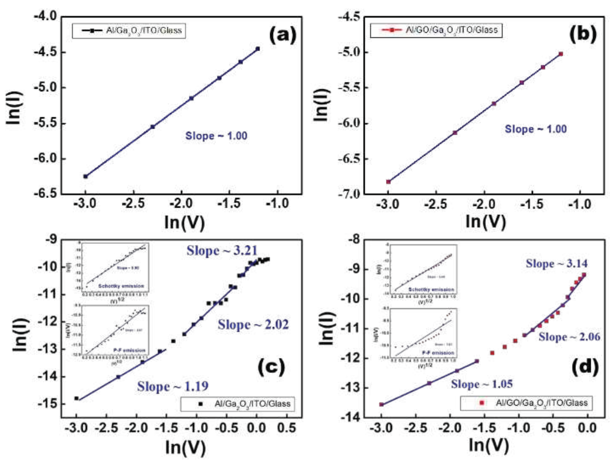
Figure 5.
(a) Endurance and (b) Retention (@T=300 K) characteristics of Ga2O3 and GO/Ga2O3 devices in HRS and LRS.
Figure 5.
(a) Endurance and (b) Retention (@T=300 K) characteristics of Ga2O3 and GO/Ga2O3 devices in HRS and LRS.
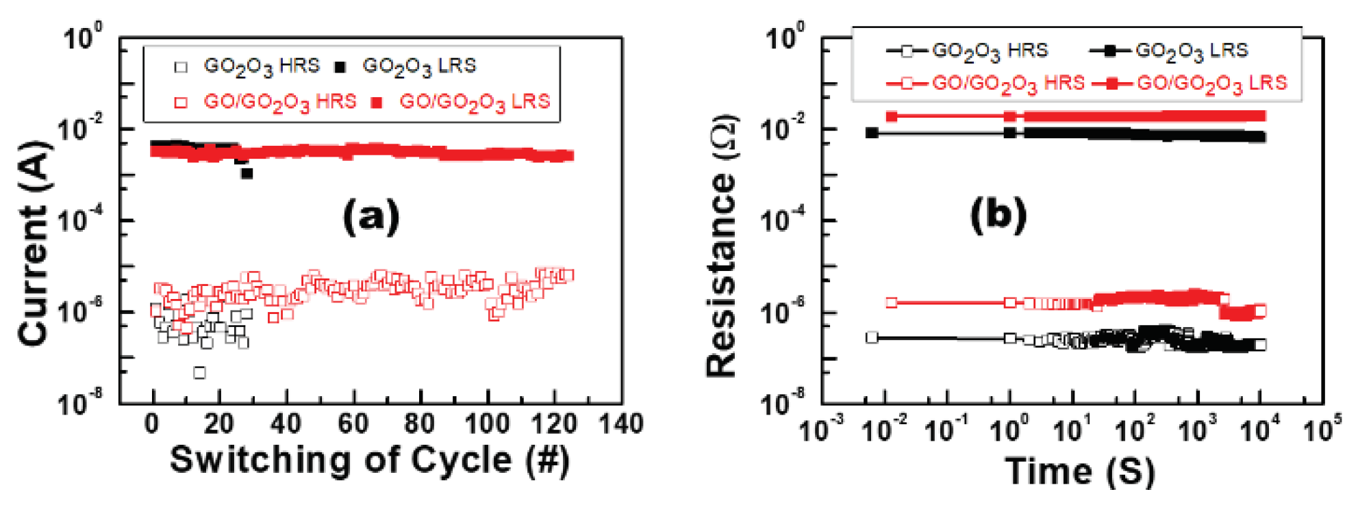
Figure 6.
(a) Cumulative probability and (b) Operation voltage distributions of HRS and LRS cycle-to-cycle in Ga2O3 and GO/Ga2O3 devices.
Figure 6.
(a) Cumulative probability and (b) Operation voltage distributions of HRS and LRS cycle-to-cycle in Ga2O3 and GO/Ga2O3 devices.
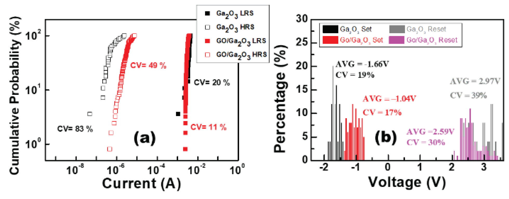
Figure 7.
The (a) I-V characteristics, (b) endurance tests, (c) retention characteristics (d) device-to-device variation for Al/GO/Ga2O3/ITO under the current compliance of 100 mA, 10mA and 1mA.
Figure 7.
The (a) I-V characteristics, (b) endurance tests, (c) retention characteristics (d) device-to-device variation for Al/GO/Ga2O3/ITO under the current compliance of 100 mA, 10mA and 1mA.
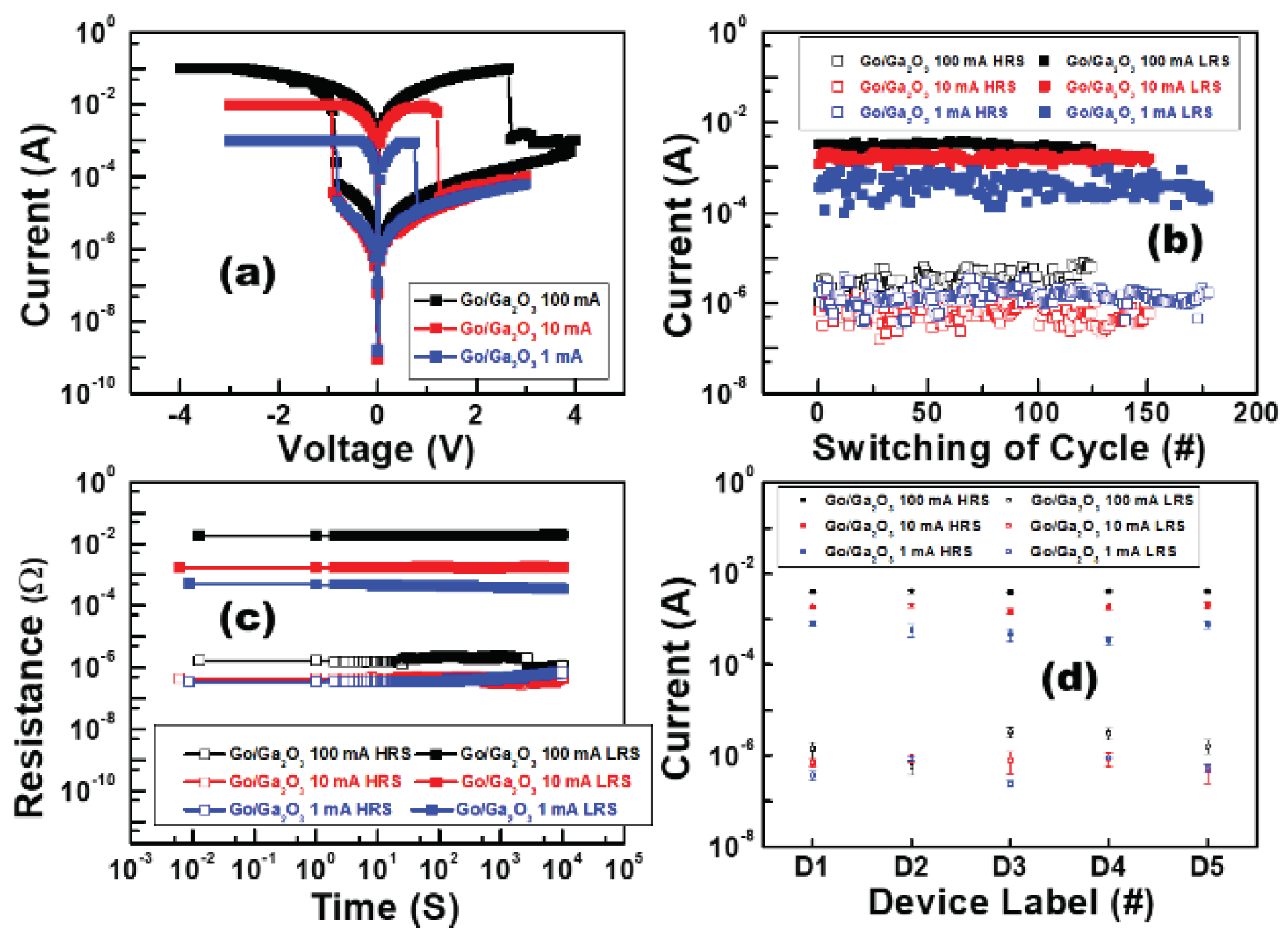
Figure 8.
Cumulative probability of HRS and LRS cycle-to-cycle in GO/Ga2O3 device at the compliance current of 100 mA, 10 mA, and 1mA, respectively.
Figure 8.
Cumulative probability of HRS and LRS cycle-to-cycle in GO/Ga2O3 device at the compliance current of 100 mA, 10 mA, and 1mA, respectively.
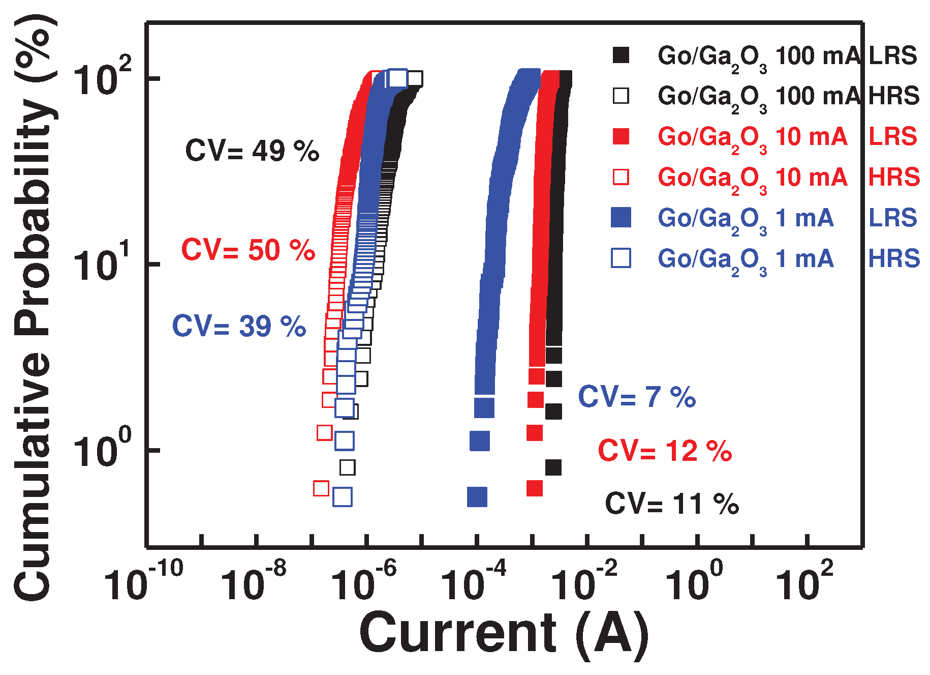
Figure 9.
Al/GO/Ga2O3/ITO/glass device at 10mA current compliance of (a) Pattern size-dependent measurement (b) Temperature-dependent resistance measured between 300 K and 500 K.
Figure 9.
Al/GO/Ga2O3/ITO/glass device at 10mA current compliance of (a) Pattern size-dependent measurement (b) Temperature-dependent resistance measured between 300 K and 500 K.
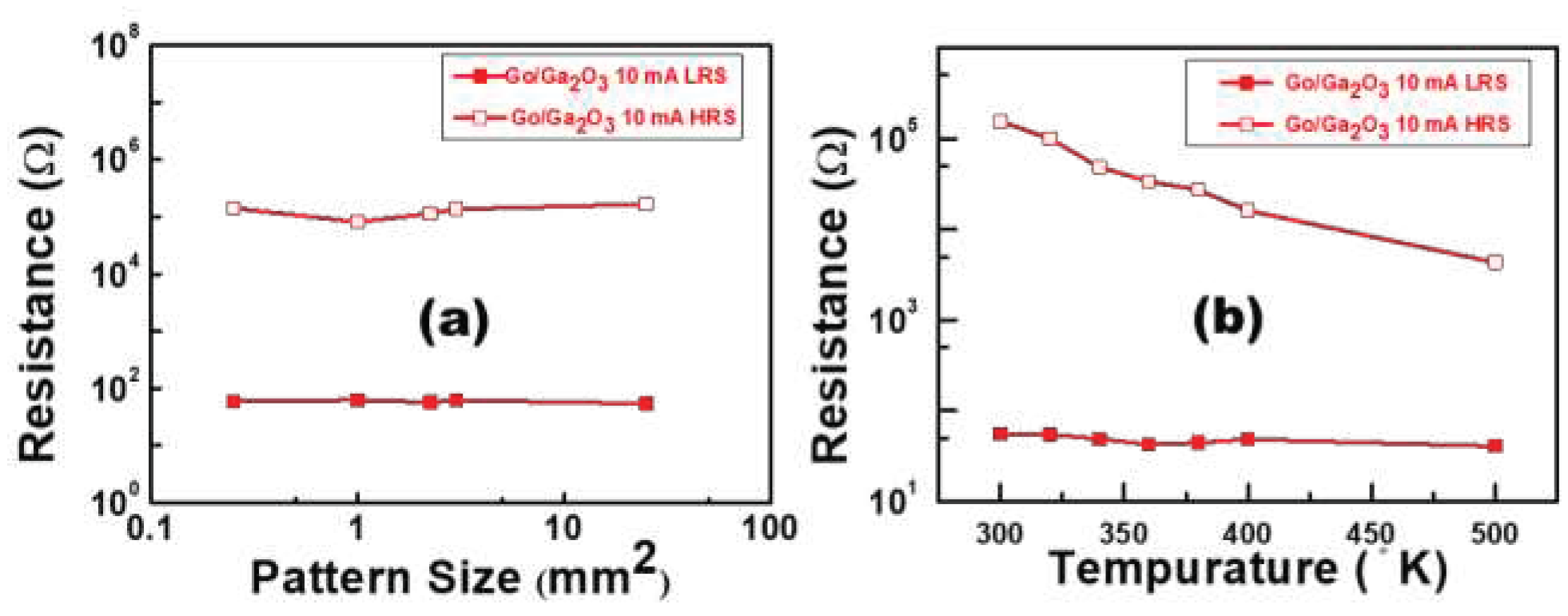
Figure 10.
Filament models of Al/Ga2O3/ITO/glass and Al/GO/Ga2O3/ITO/glass.
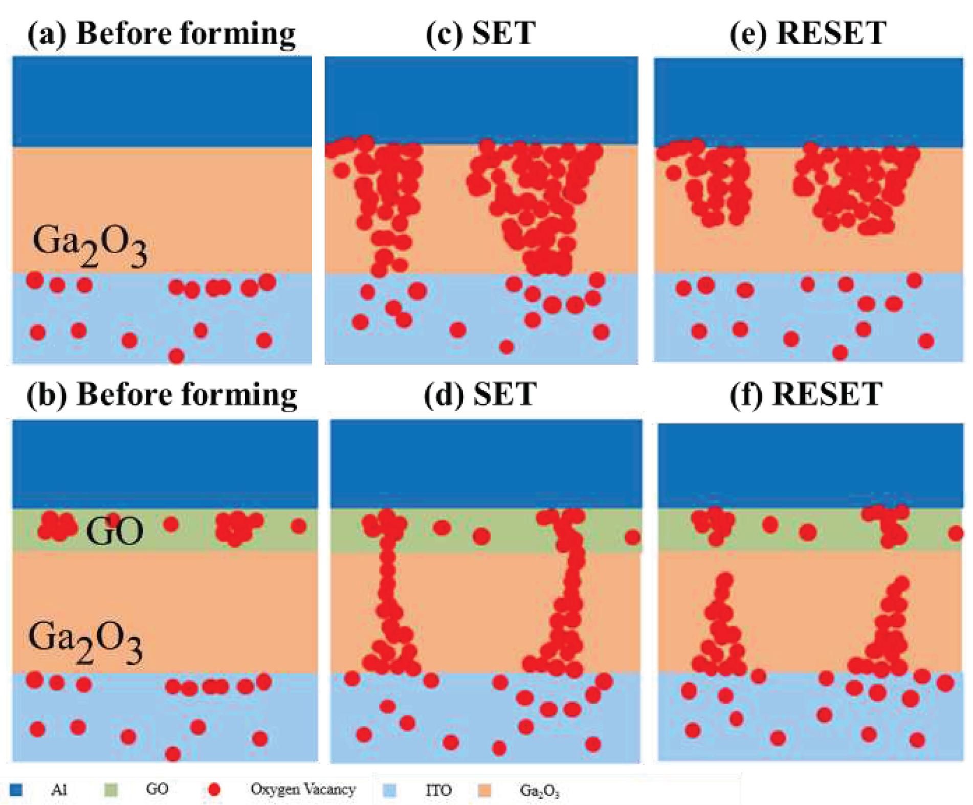
Figure 11.
(a) The schematic (b) The TEM cross-section image of Al/GO/Ga2O3/ITO/glass RRAM.
Disclaimer/Publisher’s Note: The statements, opinions and data contained in all publications are solely those of the individual author(s) and contributor(s) and not of MDPI and/or the editor(s). MDPI and/or the editor(s) disclaim responsibility for any injury to people or property resulting from any ideas, methods, instructions or products referred to in the content. |
© 2023 by the authors. Licensee MDPI, Basel, Switzerland. This article is an open access article distributed under the terms and conditions of the Creative Commons Attribution (CC BY) license (https://creativecommons.org/licenses/by/4.0/).
Copyright: This open access article is published under a Creative Commons CC BY 4.0 license, which permit the free download, distribution, and reuse, provided that the author and preprint are cited in any reuse.


