
Submitted:
05 May 2023
Posted:
06 May 2023
You are already at the latest version
Abstract
This study employed a TSMC 0.18-µm 50 V process to establish a high-voltage n-LDMOS structure. In the reference device, the number of floating-poly (poly-2) turns was 7, and the width and spacing of each turn was 1 µm. Although increasing the number of turns reduces the peak field, directly reducing or increasing the number of poly-2 turns is a common practice. The present experiment was realized in three steps, namely fixing the number of occupied area adjustment turns, adjusting the width of each turn, and adjusting the distance between turns.
The first step was fixing the number of occupied area adjustment turns. The number of turns was increased from 7 to 9, and the number of turns was reduced to 5 and 3 in the reference group. A reduction in the number of turns led to a greater decrease in the peak field and increase in the breakdown voltage despite the area remaining unchanged. A comparison of the use of three turns with that of seven turns revealed that the maximum electric field decreased by 42%, from 4.17e+3 to 2.46e+3 V/cm, and that the breakdown voltage (VBK) increased from 30.2 to 35.84 V. The second step was adjusting the width of each turn from 1 to 1.4, 1.2, 0.8, and 0.6 µm in the reference group. This increase in width reduced the maximum electric field and led to a greater increase in VBK. When the width was increased to 1.4 µm, the maximum electric field decreased by 29% from 1.95e+3 to 1.4e+3 V/cm, and the VBK increased by 183% from 30.2 to 85.6 V. The third step was adjusting the spacing of each turn from 1 to 1.4, 1.2, 0.8, and 0.6 µm in the reference group. The results revealed that a reduction in the spacing led to a greater reduction in the maximum electric field and an in-crease in the VBK. When the pitch was reduced to 0.6 µm, the maximum electric field decreased by 33%, from 1.95e+3 to 1.32e+3 V/cm, and the VBK increased by 345%, from 30.2 to 134.4 V.
Keywords:
breakdown voltage
; electric field
; floating-poly
; lattice temperature
; n-LDMOS
1. Introduction
In the rapidly developing world, the demand for larger chip sizes and improved performance is increasing. However, the protection circuits of chips can pose a serious problem. To reduce the area, the gate length is reduced, and the gate oxide layer is thinned such that it is highly susceptible to being broken by a current. Electrostatic discharge (ESD) [1,2,3,4,5,6,7] can occur because of excessive transient currents, which can be caused by the switching on of a power supply, the incomplete grounding of a machine, or human contact with an integrated circuit (IC) through human grounding (i.e., the Human Body Model). Notably, ESD can also irreversibly damage an IC. To effectively prevent ESD, specific components for power supplies and protective components for automotive electronics can be designed, and such components require advanced and improved ESD protection.
In the present study, Silvaco T-CAD software was used [8,9,10,11] to perform n-LDMOS modulation simulation. The plate effect [12,13,14,15,16,17] was employed to arrange a floating poly on the oxide layer (STI), which was used to reduce the electric field on a channel and increase the VBK. Three types of modulation were used to distinguish whether the plate effect substantially changed the components by lowering their electric fields and increasing their VBK.
2.1. The Reference Device
Figure 1 presents the structure of the reference group of components used in the present study. As indicated in the structural and layout views, the current flows from the inner drain side to the source side and bulk side, and because the ESD discharge events are all two-pin events, we connected the bulk side, source side, and gate side and grounded them to form a grounded-gate n-channel metal oxide semiconductor. In the structure, the high-voltage n-well, high-voltage p-well, and N+ formed a parasitic bipolar junction transistor (BJT) in the internal circuit, and we used this BJT as a discharge current path for discharging ESD currents. This component for the I/O PAD was designed to protect the internal component circuit when an ESD event occurs and to promptly discharge the ESD current to prevent damage to the main circuit. The high-voltage n-well forms a resistance in the drift region such that the components can operate in a high-voltage environment. Next, a poly-2 was used to create a field plate effect above the drift region to distribute the internal electric field evenly, thereby reducing the peak electric field in the drift region and increasing the breakdown voltage. The N-type buried layer structure forms an equivalent reverse diode with the p-sub below it to prevent the excessive leakage of current to the p-sub and to prevent component failure.
2.2. Field-Plate Effect
In the reference group, we used a floating poly to create a field plate effect in the component. This approach was employed to control the magnitude of the surface electric field by applying a bias to the field plate. When we applied a positive bias to the field plate, the depletion zone extended along the surface toward the edge of the field plate, which reduced the concentration effect of the original electric field and further increased the VBK.
2.3. Device Modulation Engineering
2.3.1. Fixed Area of Turns
We fixed the area occupied by the floating poly and the distance between turns to analyze the effect of the number of turns on the maximum field and VBK. Because the reference group (Ref) was a 7-turn floating poly, we increased the number of turns to 9 (S1_9R) and reduced the number of turns to 5 (S1_5R) and 3 (S1_3R) to fix the area occupied by the floating poly such that the width of each group of turns was different. The width was 0.77 μm for 9R [Figure 4a], 1 μm for Ref (Figure 1), 1.4 μm for 5R [Figure 4b], and 2.33 μm for 3R [Figure 4c].
2.3.2. Adjust Width of Each Turn
In this section, the width of each turn of the floating poly was adjusted, and the width of each turn of the reference group was 1µm. During testing, the width of each turn was increased to 1.2 (S2_1.2) and 1.4 (S2_1.4) µm, and the area occupied by each turn was increased to 8.4 and 9.8 µm, respectively. Figure 5a presents the structure formed when the width was increased to 1.4 µm. We also reduced the width to 0.8 (S2_0.8) and 0.6 (S2_0.6) µm to reduce the area occupied to 5.6 and 4.2 µm, respectively. Figure 5b presents the structure formed when the width was reduced to 0.6 µm. This experiment was performed to clarify how the area occupied by the floating poly affected the electric field value and VBK.
2.3.3. Adjusting the Spacing between Turns
In this section, the spacing of each turn of the floating poly was adjusted, and the spacing of each turn of the reference group was 1 µm. In the experiment, the spacing of each turn was increased to 1.2 (S3_1.2) and 1.4 (S3_1.4) µm and reduced to 0.8 (S3_0.8) and 0.6 (S3_0.6) µm. Figure 6a,b present the structure formed when the spacing was increased to 1.4 and 0.6 µm, respectively. This experiment was performed to clarify how increasing or decreasing the pitch of each turn of the floating poly affected the electric field value and VBK.
3. Results and Discussion
3.1. Fixed Area of Turns
Group-1 samples (S1) pertained to the adjustment to the number of turns of the fixed area; previous studies have focused on directly reducing or increasing the number of turns and have reported that a greater number of turns results in a stronger field plate effect. However, this finding indicates the presence of two variables, and whether the stronger field plate effect was due to an increase in the occupied area or the number of turns is unclear. Therefore, in the present experiment, the area occupied by the sum of the turns was fixed to exclude the effect of changing the area occupied and to clarify the effect of changing the number of turns on ESD capability. Table 1 presents the data for the S1 injection current 1E-4 A. The table reveals that the trigger voltage (Vt1) tended to increase when the number of turns was reduced; this occurred because we used the field plate effect to reduce the strength of the electric field in the channel, which made it more difficult for components to conduct electricity and caused Vt1 to increase. Figure 7 presents the Vt1 and VBK trends of the S1 samples. S1_3R (i.e., fewest number of turns) had the highest Vt1 of 146.6 V, and S1_9R had the lowest Vt1 of 50.8 V. When the Vt1 increased, the VBK also increased, with the highest and lowest VBK of 69.9 and 30.2 V, respectively, being achieved with S1_3R and S1_9R, respectively. The lattice temperature floated at 725 K, indicating that changing the number of turns did not cause the lattice temperature to change.
In this work, an accurate measurement of the maximum electric field value of the metal oxide semiconductor could not be obtained because of the field plate effect. Therefore, we obtained a sample at the center of the channel under the STI layer and placed a star marker at 22.8 on the X-axis to compare the field strengths. Figure 8 presents the trend for the S1 star point EF between the groups, and the results revealed that the lowest star point EF value of 2.46e+3 V/cm was obtained when the number of turns was reduced to 3 (S1_3R). Relative to the 3-turn star point EF, the 5-turn (S1_5R) star point EF increased slightly to 4.02e+3 (V/cm). When the number of turns was increased to 9 (S1_9R), the highest star point EF of 7.46e+3 V/cm was obtained. From these simulation data reveals that when the occupied area was fixed, reducing the number of turns reduced the field value.
3.2. Adjust Width of Each Turn
Group-2 samples (S2) pertained to the width adjustment for each turn. In contrast to the previous section, where the area occupied was fixed, the number of turns was fixed in S2 to clarify how increasing the occupied area affected the ESD components. Table 2 presents the data for the S2 injection current 1E-4A. The table reveals that the Vt1 increased when the turn width was increased. This likely occurred because an increase in the area occupied created a stronger field plate effect, which made it more difficult for the components to conduct electricity and caused the Vt1 to increase. The Vt1 was 89.8 V at the widest width of 1.4 (S2_1.4) µm. The Vt1 of the reference group was 57.94 V when the width was 1 (S2_ref) µm; this value differed from that of the reference group in the previous section. This could have occurred because increasing the width to 1.4 µm caused overlapping with the poly-1 layer to the right. Thus, shifting the floating poly to the left by 1 µm caused the value of the reference group to deviate. When the width decreased to 0.6 (S2_0.6) µm, the Vt1 also decreased to 31.4 V. The VBK also changed when the Vt1 changed. When the width was 1.4 (S2_1.4) µm, the VBK was 85.5 V, and the Vt1 of the reference group (S2_ref) was 30.2 V. At the narrowest width of 0.6 (S2_0.6) µm, the Vt1 decreased to only 8.7 V. Figure 9 presents Vt1 and VBK trends of the S2 for each device when the lattice temperature was maintained at 725 K. Furthermore, the lattice temperature was not affected by adjustments to the width of the aforementioned section.
The collected data indicated that the electric field started to weaken when the width increased and that the star point EF of the reference group (S2_ref) was 1.95e+3 V/cm. After the width was reduced, the star point EF was 4.12e+3 V/cm at the smallest width of 0.6 (S2_0.6) µm. The star point EF was 2.48e+3 V/cm for S2_0.8. The star point EF of S2_1.2 was 1.8e+3 V/cm at the widest width of 1.2 (S2_1.2) µm. The star point EF at the widest width of 1.4 (S2_1.4) µm was 1.4e+3 V/cm. Figure 10 presents the star point EF comparison of S2 samples.
3.3. Adjusting the Spacing between Turns
This subsection group pertained to adjustments of the spacing between turns and the width of each turn after the width of each turn was fixed. Table 3 presents the data for the S3 samples as the injection current 1E-4A. By observing the Vt1, we determined whether reducing spacing would lead to an increase in the Vt1. Figure 11 presents a comparison of the trends between the Vt1 and VBK of the groups in S3. When the spacing was reduced to 0.6 (S3_0.6) µm, the Vt1 increased to 158.4 V. When the spacing was 1 (S3_ref) µm, the Vt1 was 57.94 V, which is identical to the Vt1 in the reference group (discussed in the previous subsection) when the spacing and width were both 1 µm. When the spacing was increased to 1.4 (S3_1.4) µm, the Vt1 decreased to 31.4 V. The VBK and Vt1 followed the same trend; that is, with a minimum spacing of 0.6 (S3_0.6) µm, the VBK was 134.4 V [reference group (S3_ref) VBK = 30.2 V], and with a maximum spacing of 1.4 (S3_1.4) µm, the VBK was 8.7 V. Similar to the findings for the Vt1, the VBK increased and decreased when the spacing was reduced and increased, respectively, with the lowest value being 8.7 V. The lattice temperature was not affected by changes in the floating poly; this finding is supported by those of the previous subsections.
With respect to the electric field values, the reference group (S3_ref) produced a 1.95e+3-V/cm electric field, which corresponds to the values reported in the previous subsection, and reducing the pitch caused the electric field to weaken. With a pitch of 0.6 (S3_0.6) µm, the star point EF was 1.54e+3 V/cm. With a spacing of 0.8 (S3_0.8) µm, the star point EF was 1.65e+3 V/cm. When the spacing was increased, the electric field strengthened. With a spacing of 1.2 (S3_1.2) µm, the star point EF was 2.56e+3 V/cm. With a spacing of 1.4 (S3_1.4) µm, the star point EF was 3.42e+3 V/cm. Figure 12 presents the star point EF comparison of S3 samples., and it reveals that an increase in the spacing reduced the field effect, resulting in higher field values and lower VBK values.
3.4. Comparison of Electric Field Values by Different Groups
This work is intended to reduce the electric field in the channel by adjusting it with a Floating poly. It is generally accepted that the more the number of turns, the more significant the reduction of the field. The conditions can be subdivided into the total area occupied by the Floating poly, the number of turns, or the width and spacing of the turns, all of which may affect the protection capacity. In S1 (fixed area of turns) we fixed the occupied area, increased the number of turns, and organized the EF field distribution to produce Figure 13. However, it can also be seen that the width of the circles increases as the number decreases.
Therefore, we have fixed the number of turns for S2 and S3 to investigate the effect of width and pitch on the protection capability. The EF field values for S2 (width adjustment) and S3 (pitch adjustment) are plotted in Figure 14, which shows that the wider the width, the lower the field, and the greater the pitch, the higher the field. Therefore, the higher the width of the protection element and the lower the spacing, the greater the reduction of the electric field (EF) value.
4. Conclusions
The present study focused on a floating poly. In S1 group, this study fixed the occupied area and adjusted the number of turns to analyze how changing the number of turns while the overall occupied area was fixed would affect the components’ ESD protection capability. Through the experiments, we discovered that when the number of turns was reduced, the area occupied by each turn increased, resulting in a stronger plate effect and, therefore, a weaker field and higher VBK. When the number of turns was 9 (S1_9R), which was the maximum number of turns, the VBK was 30.2 V, and the electric field value (star point EF) at the center of the channel was 7.46e+3 V/cm. When the number of turns was 3 (S1_3R), which was the minimum number of turns, the VBK was 66.9 V, and the star point EF was 2.46e+3 V/cm. The VBK increased by 121%, and the electric field decreased by 33%. The optimal results for the ESD protection components were obtained when the number of turns was 3 (S1_3R) and the turn width was higher.
In S2 group, the number of turns was fixed, and the width of each turn was changed to clarify how width changes affected the occupied area on the component. When the width was 1.0 (S2_ref) µm, the VBK was 30.2 V, and the star point EF was 1.95e+3 V/cm. When the width was 0.6 (S2_0.6) µm, the VBK was 8.7 V, which was the lowest VBK observed, and the star point EF was 4.12e+3 V/cm, which was the highest star point EF observed. This star point EF was 71% lower and 111% higher than those of the reference group and the electric field, respectively. These results were considered unfavorable. When the width was increased to 1.4 (S2_1.4) µm, the VBK of the reference group increased by 283% to 85.5 V, and the electric field value decreased by 29% to 1.4e+3 V/cm. Therefore, increasing the width of each turn increased the strength of the field effect and enhanced the ESD protection of the component.
In S3 group, the number of turns and width were fixed and the spacing of each turn was adjusted to determine how the distance of between field boards affected the ESD capability of the components. The reference group (S3_ref) and S2 had the same width (1.0 µm) and spacing (1.0 µm); thus, the values for both groups were identical. When the pitch was reduced to 0.6 (S3_0.6) µm, the VBK was 134.4 V, and the star point EF was 1.54e+3 V/cm, indicating that compared with the reference group, in the S3_0.6, the VBK increased by 445% and the electric field value decreased by 33%. When we increased the spacing to 1.4 (S3_1.4) µm, the VBK was 8.7 V, and the star point EF was 3.42e+3 V/cm. Compared with the reference group, in S3_1.4, the VBK decreased by 72%, and the electric field value increased by 75%. The farther the spacing was, the weaker was the field plate effect.
In conclusion, the field plate effect increased the floating-poly level. When the area occupied by each turn decreased, the width of each turn increased, and when the spacing between turns decreased, the field plate effect strengthened. These findings indicate that reducing the electric field value in the channel or increasing the VBK can lead components to exhibit improved ESD resistance.
References
- Liu, J.; Liu, Y.; Han, A.; Nie, Y.; Huang, Q.; Liu, Z. A Novel Voltage Divider Trigger SCR With Low Leakage Current for Low-Voltage ESD Application. IEEE Trans. Electron Devices 2022, 69, 2534–2542. [CrossRef]
- Do, K. -I.; Song, B. -B.; Koo, Y. -S. A Gate-Grounded NMOS-Based Dual-Directional ESD Protection with High Holding Voltage for 12V Application. IEEE Trans. Device Mater. Reliab. 2020, 20, 716–722. [CrossRef]
- Lai, D. -W.; Sque, S.; Peters, W.; T. Smedes.Gate-Lifted nMOS ESD Protection Device Triggered by a p-n-p in Series with a Diode. IEEE Trans. Electron Devices 2019, 66, 1642–1647. [CrossRef]
- Lee, J. -H.; Prabhu, M.; Natarajan, M.I. Engineering ESD Robust LDMOS SCR Devices in FinFET Technology. IEEE Electron Device Lett. 2018, 39, 1011–1013. [CrossRef]
- Huang, C. -Y.; Chiu, F. -C.; Ou, C. -M.; Chen, Q. -K.; Huang, Y. -J.; Tseng, J. -C. ESD and Latchup Optimization of an Embedded-Floating-pMOS SCR-Incorporated BJT. IEEE Trans. Electron Devices 2016, 63, 3036–3043. [CrossRef]
- Lin, C. -Y.; Chang, P. -H.; Chang, R. -K. Improving ESD Robustness of pMOS Device with Embedded SCR in 28-nm High- $k$ /Metal Gate CMOS Process. IEEE Trans. Electron Devices 2015, 62, 1349–1352. [CrossRef]
- Wu, C. -H.; Lee, J. -H.; Lien, C. A Novel Drain Design for ESD Improvement of UHV-LDMOS. IEEE Trans. Electron Devices 2015, 62, 4135–4138. [CrossRef]
- Hasan, T.; Zafar, S.; Ozbay, E.U.; Kashif, A. Analysis of HfO2 and ZrO2 as High-K Dielectric for CMOS Nano Devices. In Proceedings of the 2022 9th International Conference on Electrical and Electronics Engineering (ICEEE), Alanya, Turkey, 2022; pp. 99–103. [CrossRef]
- Khadir, A.; Kouzou, A.K.; Abdelhafidi, M. Effect of Anti-Reflective Coating on CIGS Solar Cells Performance. In Proceedings of the 2020 17th International Multi-Conference on Systems, Signals & Devices (SSD), Monastir, Tunisia, 2020; pp. 621–625. [CrossRef]
- Dutta, R.; Tamang, T.; Paul, P.; Paitya, N.; Comparative Study of AlGaN/GaN, InAlN/GaN and AlGaAs/GaAs based High Electron Mobilty Transistors Using Silvaco for High-Frequency Applications. In Proceedings of the 2020 4th International Conference on Trends in Electronics and Informatics (ICOEI)(48184), Tirunelveli, India, 2020; pp. 137–142. [CrossRef]
- Li, S.; Tian, Y.; Wei, J.; Liu, S.; Sun, W. Electrical parameters shifts of 1.2kV 4H-SiC MOSFET under cosmic radiations. In Proceedings of the 2017 IEEE 24th International Symposium on the Physical and Failure Analysis of Integrated Circuits (IPFA), Chengdu, China, 2017; pp. 1–4. [CrossRef]
- Wang, R.; Qiao, M.; Wang, Y.; Li, Z.; Zhang, B.Novel High-Tolerance Termination With Resistive Field Plate for 600 V Super-Junction Vertical Double-Diffused MOSFET. IEEE Electron Device Lett. 2022, 43, 1093–1096. [CrossRef]
- Duan, B.; Xue, S.; Huang, X.; Yang, Y. Novel Si/SiC Heterojunction Lateral Double-Diffused Metal Oxide Semiconductor with SIPOS Field Plate by Simulation Study. IEEE J. Electron Devices Soc. 2021, 9, 114–120. [CrossRef]
- Zhen, Z.; Feng, C.; Wang, Q.; Niu, D.; Wang, X.; Tan, M. Single Event Burnout Hardening of Enhancement Mode HEMTs with Double Field Plates. IEEE Trans. Nucl. Sci. 2021, 68, 2358–2366. [CrossRef]
- Kilpi, O. -P.; Andrić, S.; Svensson, J.; Ram, M.S.; Lind, E.; Wernersson, L. -E. Increased Breakdown Voltage in Vertical Heterostructure III-V Nanowire MOSFETs with a Field Plate. IEEE Electron Device Lett. 2021, 42, 1596–1598. [CrossRef]
- Liu, H. et al. Characteristics of partial discharge in oil-paper insulated needle plate electrode model under composite AC-DC voltage. CSEE J. Power Energy Syst. 2020, 6, 848–857. [CrossRef]
- Zhang, W. et al. Model and Experiments of Small-Size Vertical Devices with Field Plate. IEEE Trans. Electron Devices 2019, 66, 1416–1421. [CrossRef]
Figure 1.
Cross-sectional view of the high voltage nLDMOS reference device.
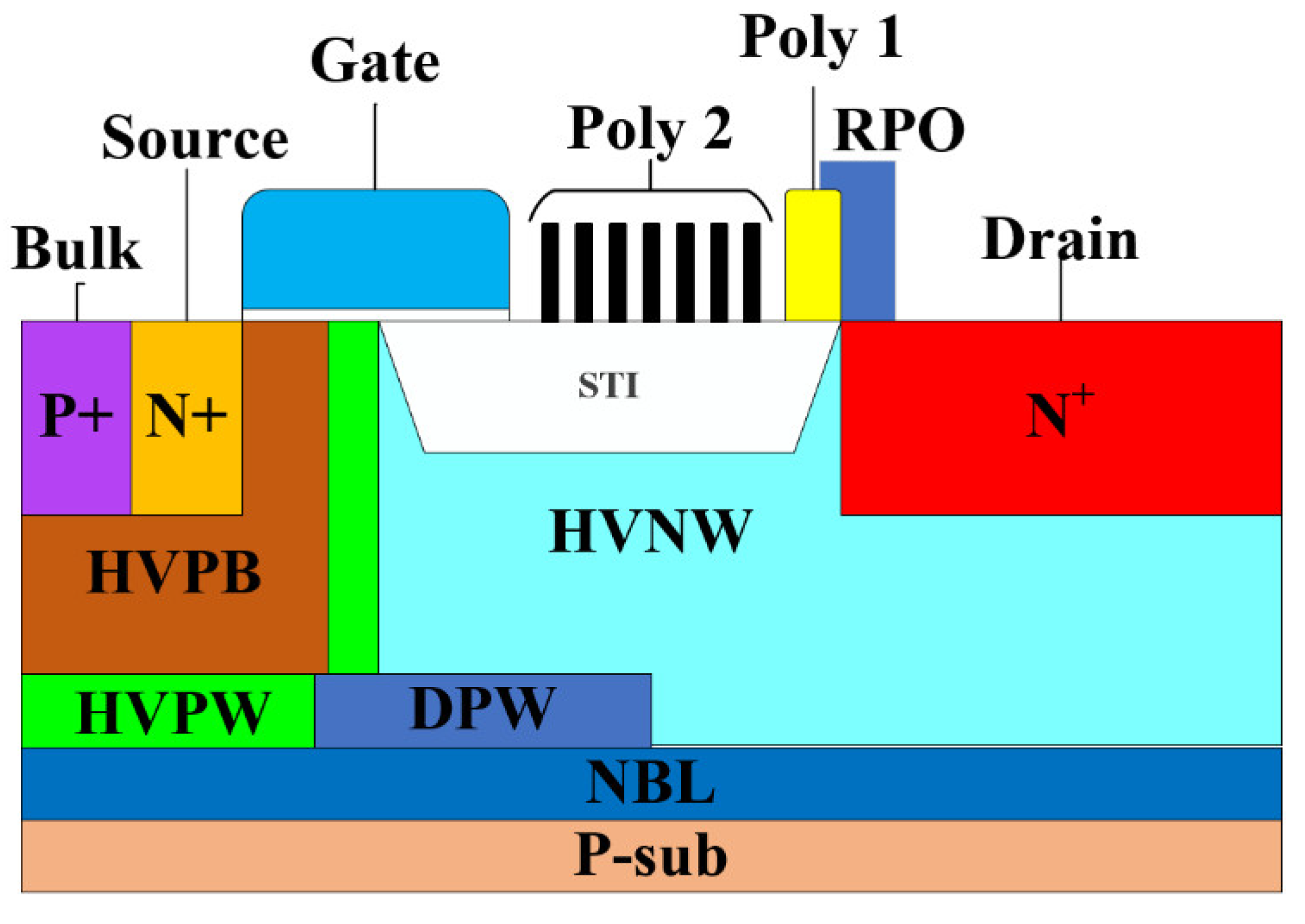
Figure 2.
Field plate structure with a continuous field plate.
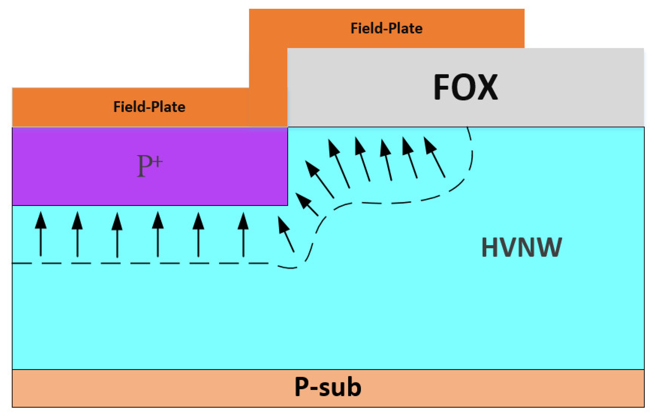
Figure 3.
Field plate structure with a floating field plate.
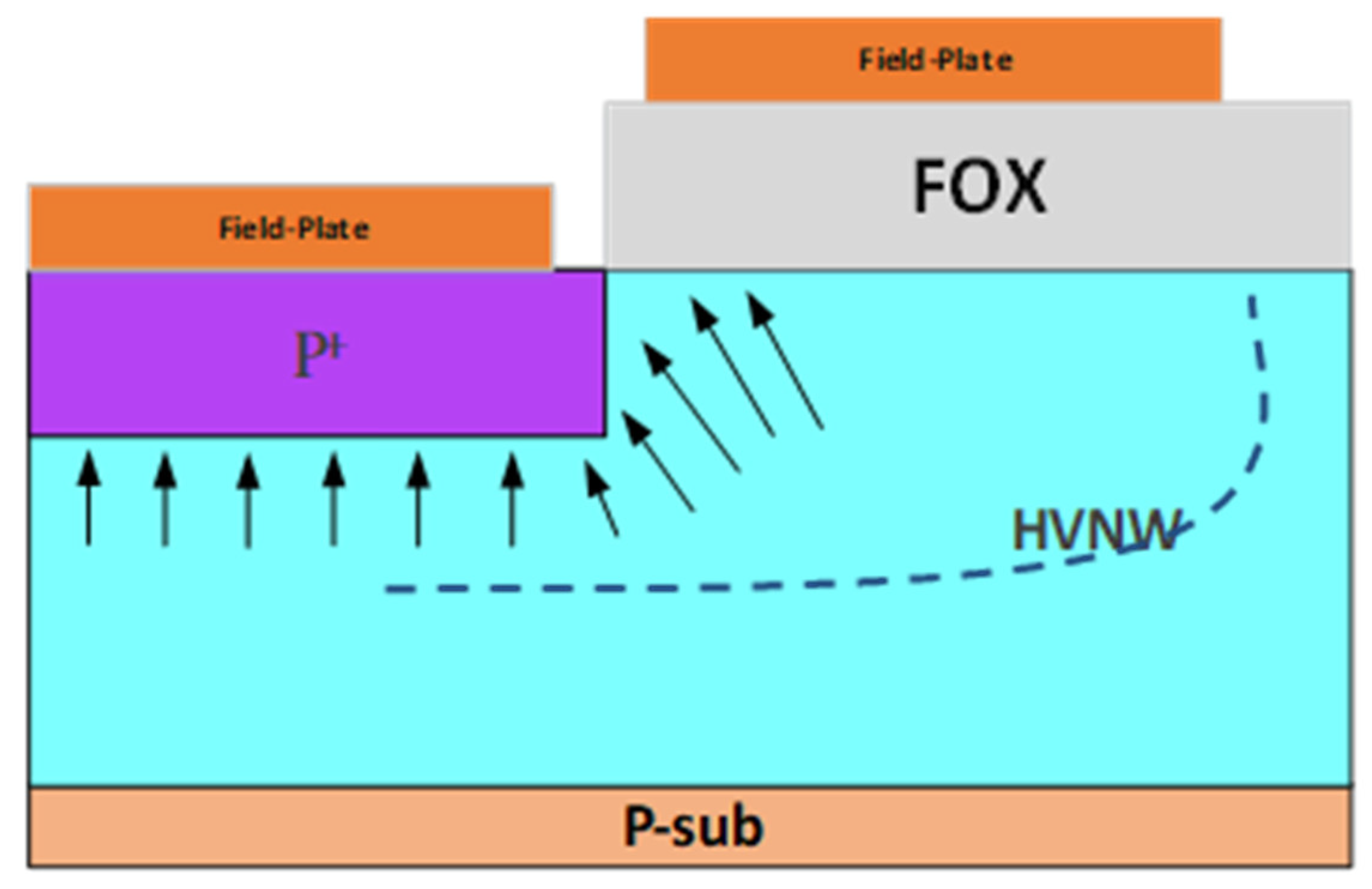
Figure 4.
Cross-sectional views of the high voltage nLDMOS (a) S1_9R, (b) S1_5R and (c) S1_3R devices.
Figure 4.
Cross-sectional views of the high voltage nLDMOS (a) S1_9R, (b) S1_5R and (c) S1_3R devices.
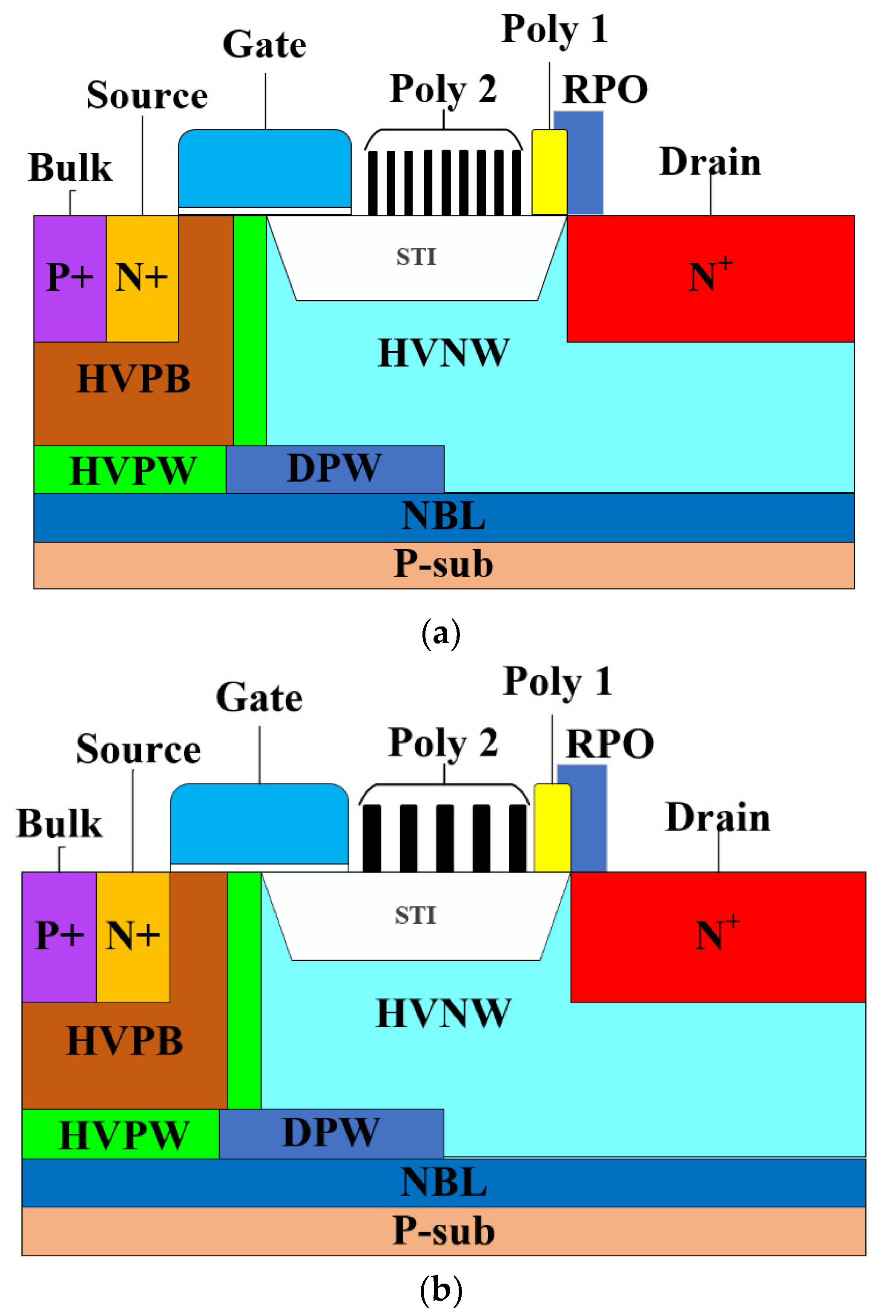
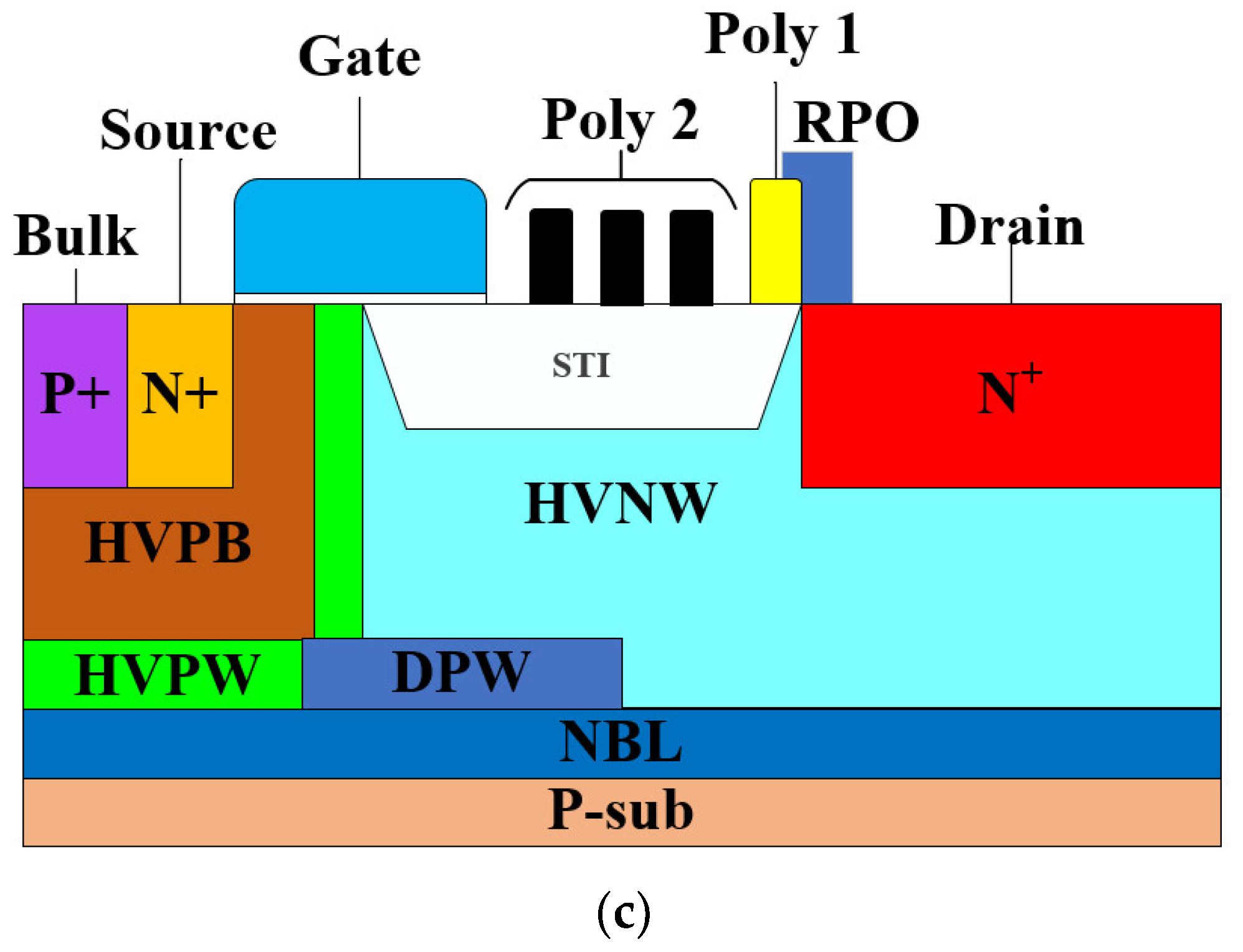
Figure 5.
Cross-sectional views of the high voltage nLDMOS (a) S2_1.4 and (b) S2_0.6 devices.
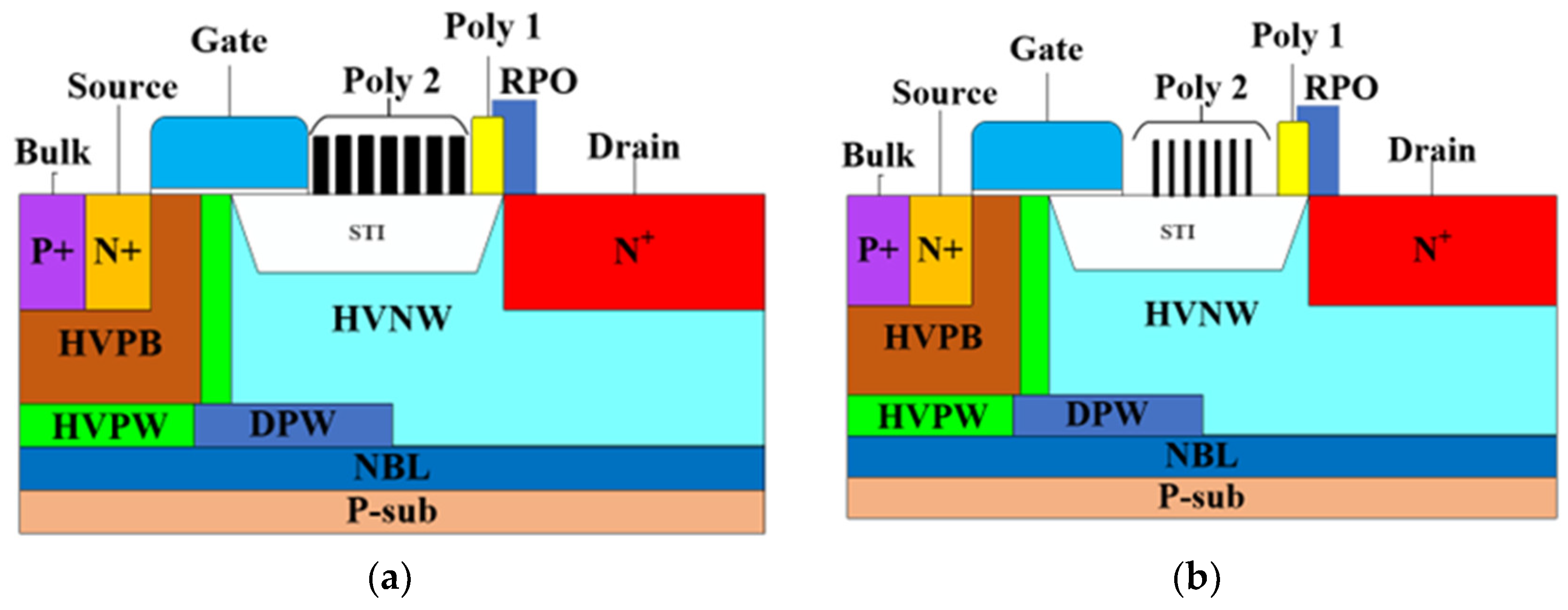
Figure 6.
Cross-sectional views of the high voltage nLDMOS (a) S3_1.4 and (b) S3_0.6 devices.
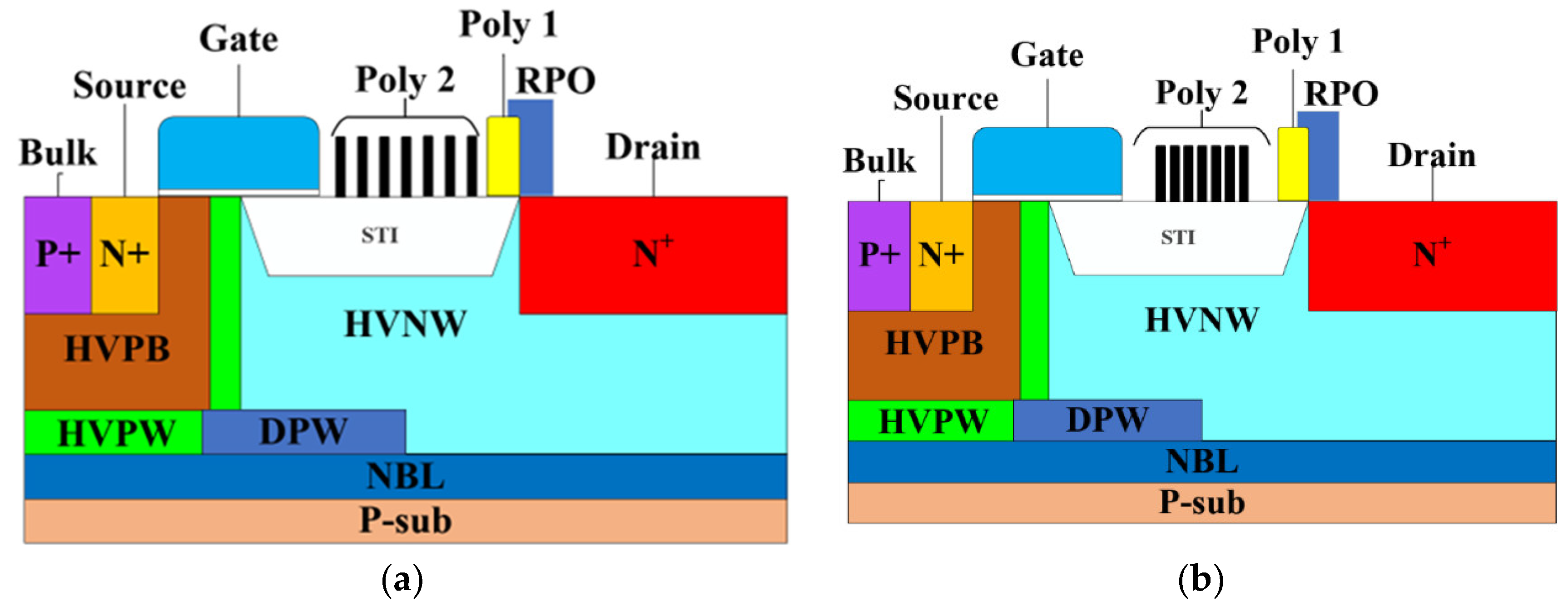
Figure 7.
S1 trend graphs of Vt1 and Vbk values.
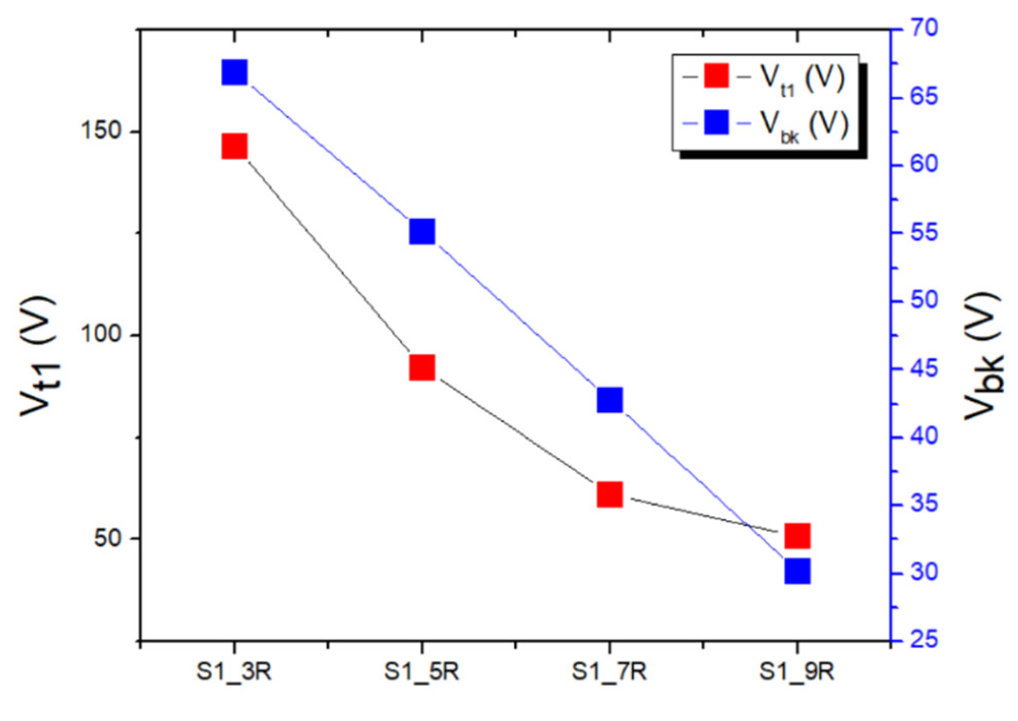
Figure 8.
S1 star point EF trend between these related devices.
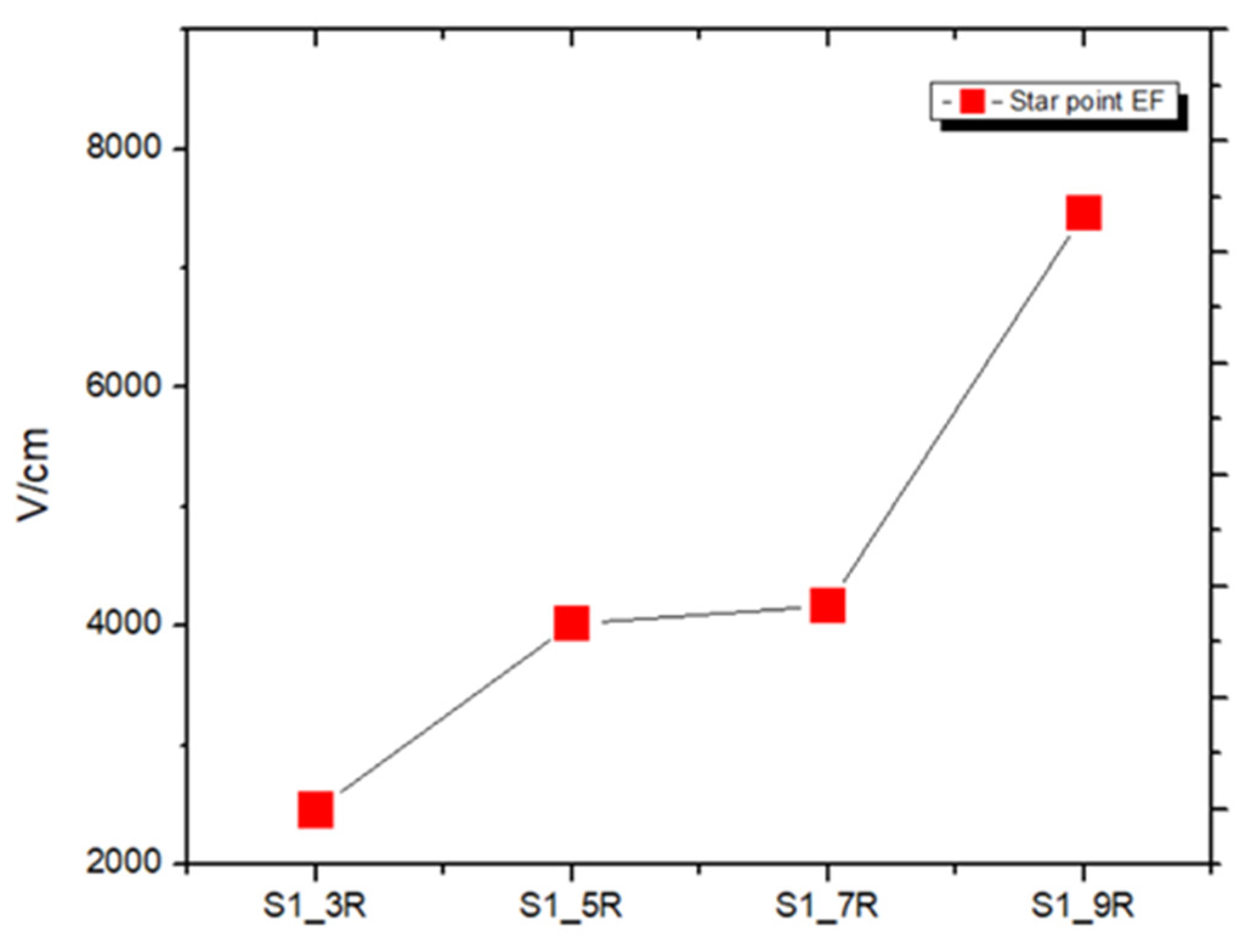
Figure 9.
S2 trend graphs of Vt1 and Vbk values.
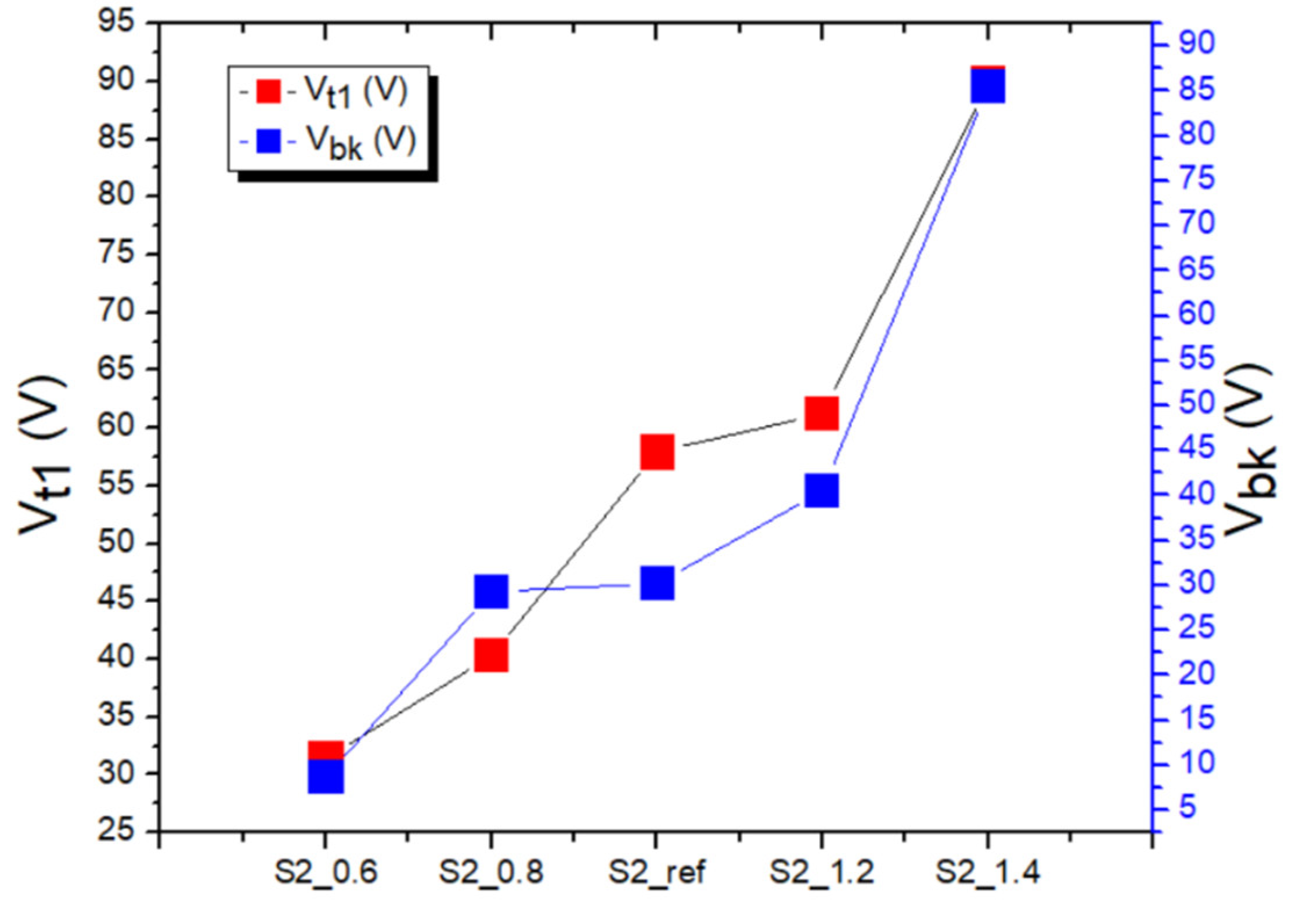
Figure 10.
S3 Star point EF trend between these related devices.
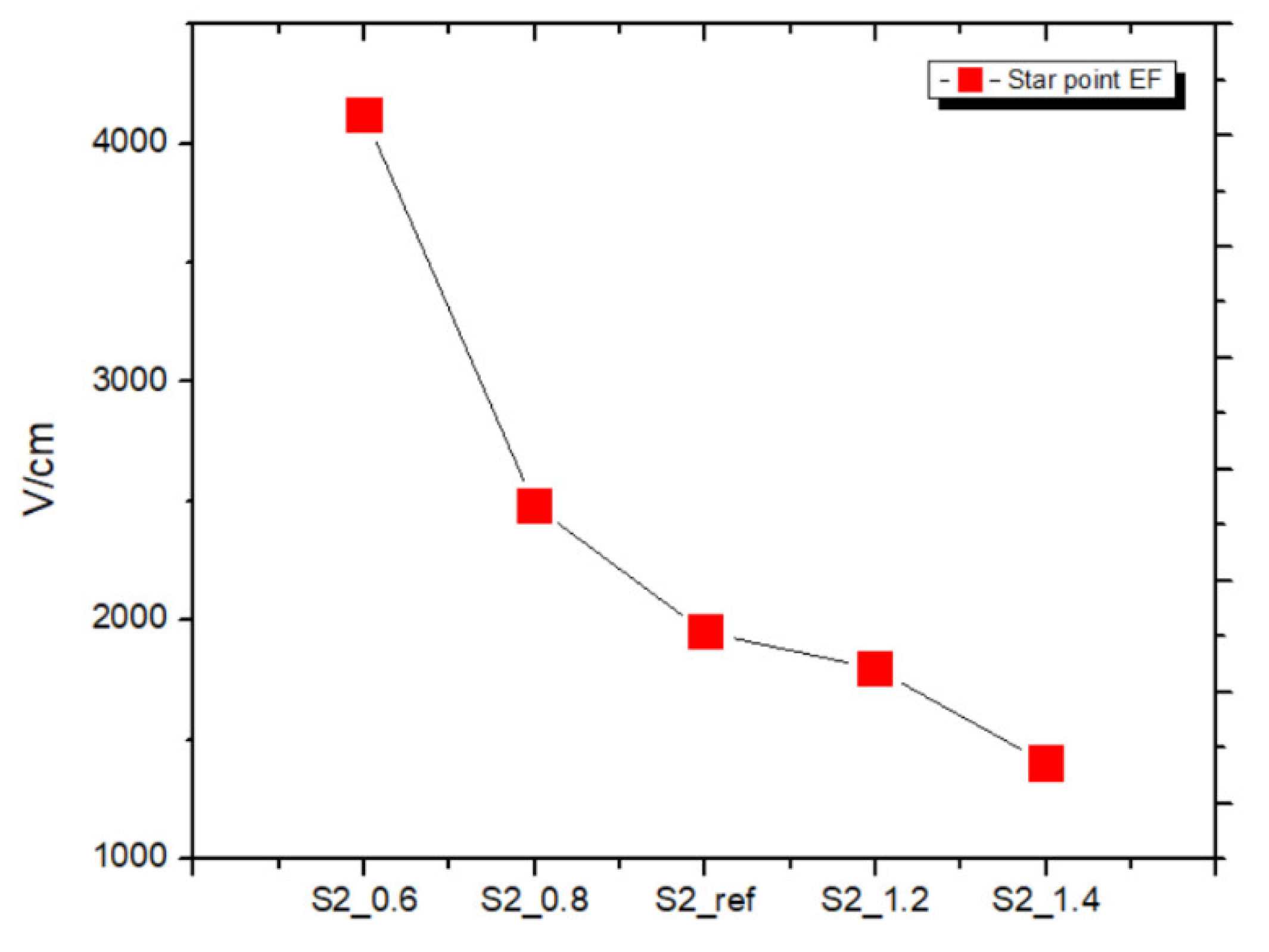
Figure 11.
S3 trend graphs of Vt1 and Vbk values.
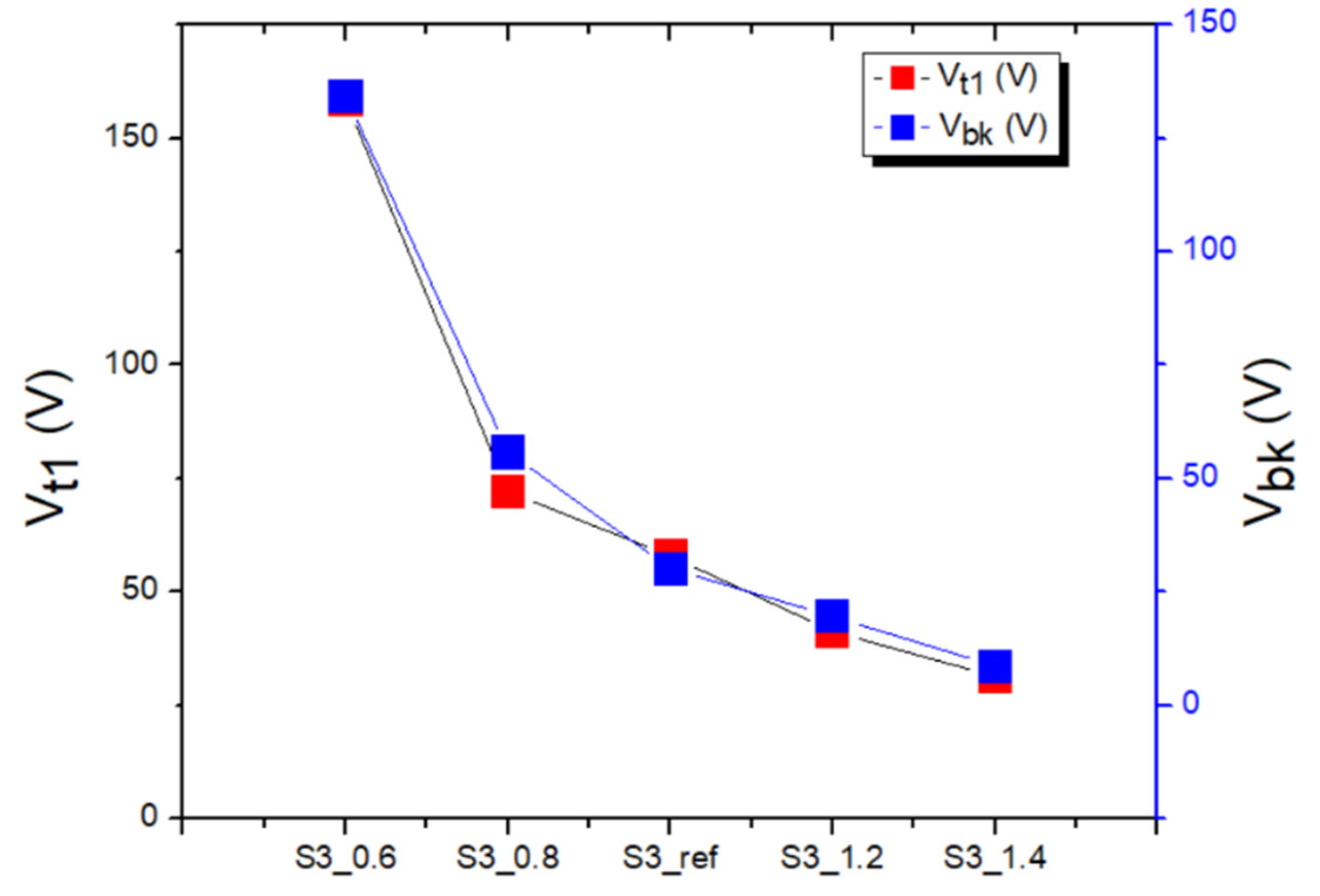
Figure 12.
S3 star point EF trend between these related devices.
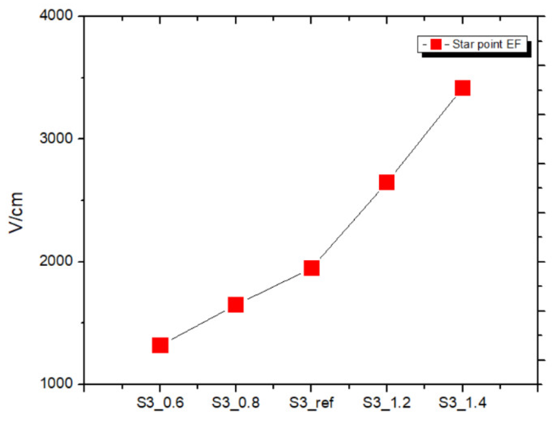
Figure 13.
S1 electric field (EF) values in the channel.
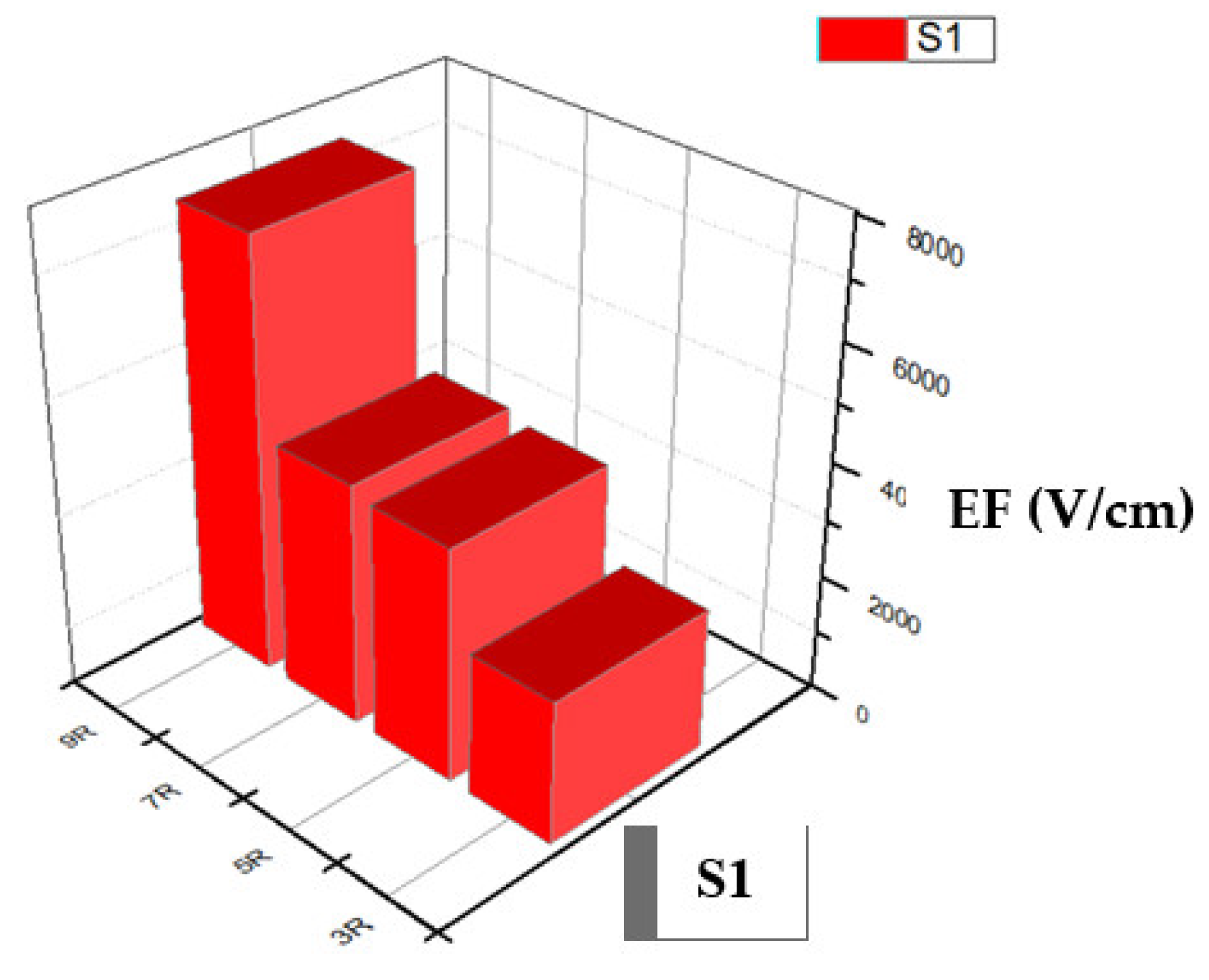
Figure 14.
S2 & S3 electric field (EF) values in the channel.
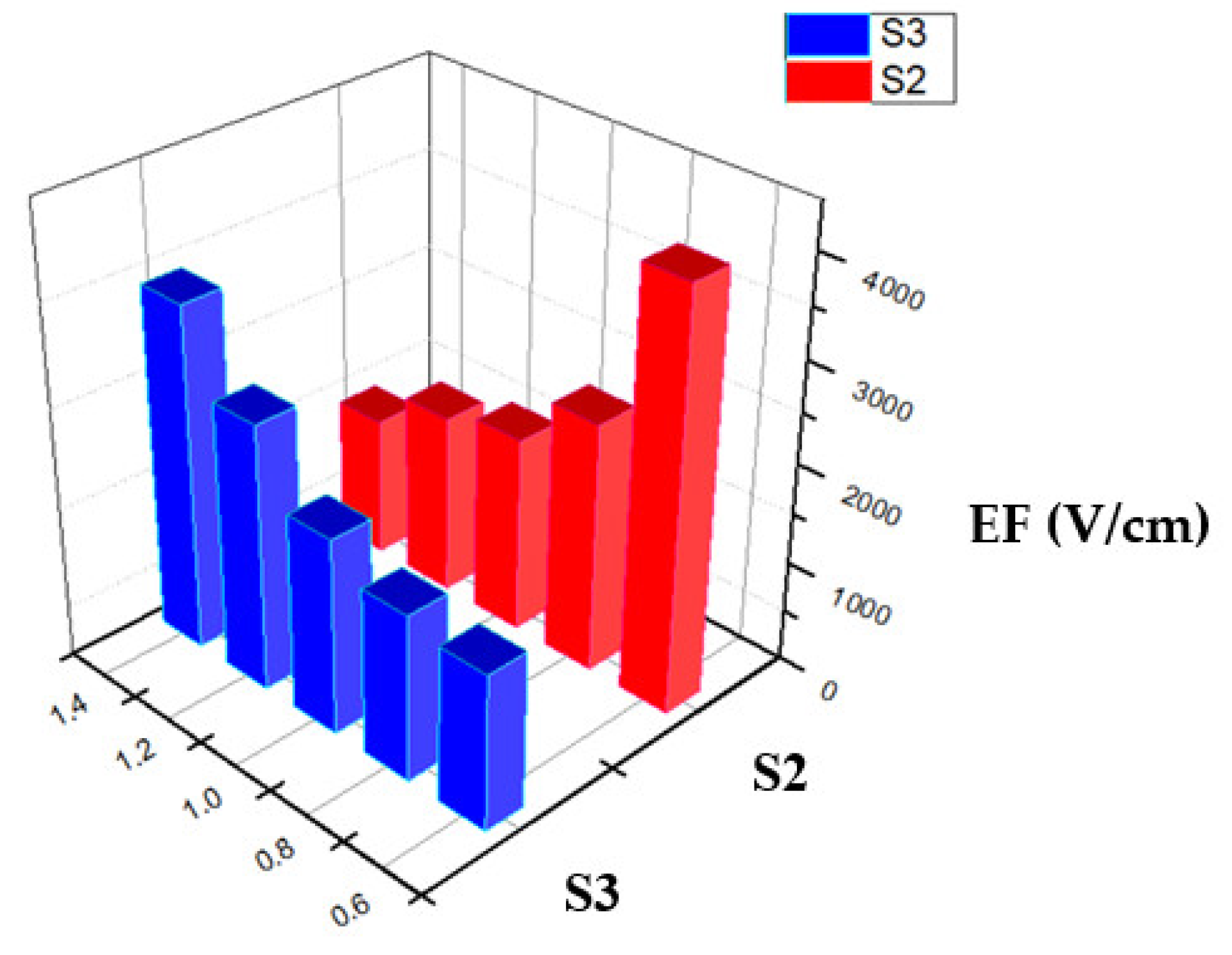

Table 1.
Device data of the S1 samples as the injection current 1E-4A.
| S1_samples | Vt1 (V) | It2 (A) | Star EF (V/cm) | Lattice Temp (K) | Breakdown (V) |
| S1_3R | 146.6 | 1.36 | 2.46e+3 | 725 | 66.9 |
| S1_5R | 92.3 | 1.43 | 4.02e+3 | 726 | 55.2 |
| S1_7R | 61.2 | 1.47 | 4.17e+3 | 725 | 42.8 |
| S1_9R | 50.8 | 1.54 | 7.46e+3 | 725 | 30.2 |
Table 2.
Device data of the S2 samples as the injection current 1E-4A.
| S2_samples | Vt1 (V) | It2 (A) | Star EF (V/cm) | Lattice Temp (K) | Breakdown (V) |
| S2_0.6 | 31.4 | 1.45 | 4.12e+3 | 725 | 8.7 |
| S2_0.8 | 40.3 | 1.46 | 2.48e+3 | 725 | 29.3 |
| S2_ref | 57.94 | 1.4 | 1.95e+3 | 725 | 30.2 |
| S2_1.2 | 61.24 | 1.53 | 1.8e+3 | 725 | 40.5 |
| S2_1.4 | 89.8 | 1.55 | 1.4e+3 | 725 | 85.5 |
Table 3.
Device data of the S3 samples as the injection current 1E-4A.
| S3_samples | Vt1 (V) | It2 (A) | Star EF (V/cm) | Lattice Temp (K) | Breakdown (V) |
| S3_0.6 | 158.4 | 1 | 1.54e+3 | 725 | 134.4 |
| S3_0.8 | 72.14 | 1 | 1.65e+3 | 725 | 55.8 |
| S3_ref | 57.94 | 1.4 | 1.95e+3 | 725 | 30.2 |
| S3_1.2 | 41.3 | 1.42 | 2.65e+3 | 725 | 19.6 |
| S3_1.4 | 31.4 | 1.50 | 3.42e+3 | 724 | 8.7 |
Disclaimer/Publisher’s Note: The statements, opinions and data contained in all publications are solely those of the individual author(s) and contributor(s) and not of MDPI and/or the editor(s). MDPI and/or the editor(s) disclaim responsibility for any injury to people or property resulting from any ideas, methods, instructions or products referred to in the content. |
© 2023 by the authors. Licensee MDPI, Basel, Switzerland. This article is an open access article distributed under the terms and conditions of the Creative Commons Attribution (CC BY) license (https://creativecommons.org/licenses/by/4.0/).
Copyright: This open access article is published under a Creative Commons CC BY 4.0 license, which permit the free download, distribution, and reuse, provided that the author and preprint are cited in any reuse.


